

amily
查询CY62128V供应商
CY62128V Family
128K x 8 Static RAM
Features
• Low volt age rang e :
—2.7V–3.6V (CY62128V)
—2.3V–2.7V (CY62128V25)
—1.6V–2.0V (CY62128V18)
• Low active power and standby power
• Easy memory expansion wit h CE
and OE fe atures
• TTL-compatible inputs and outputs
• Aut om atic power-d ow n when deselected
• CMOS for optimum speed/power
Functional Description
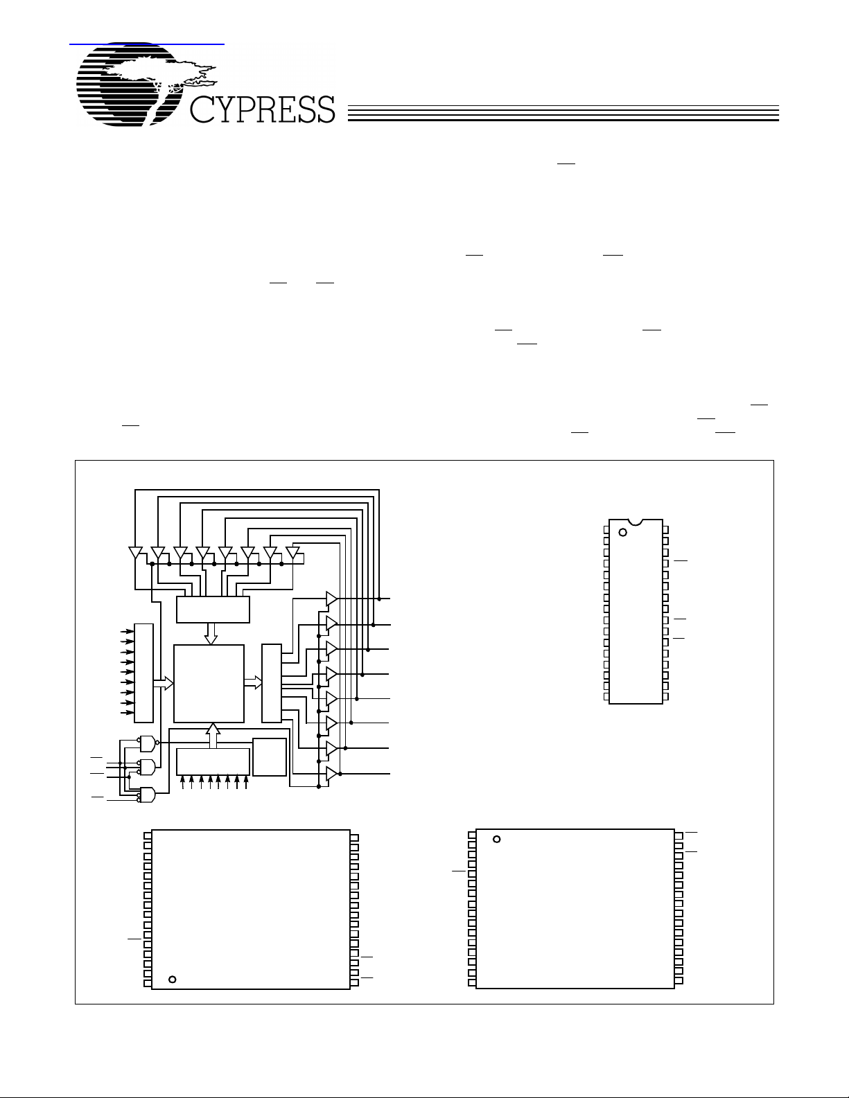
The CY62128V f ami ly i s com posed of three hi gh-per formanc e
CMOS static RAMs organized as 131,072 words by 8 bits.
Easy memory expansion is provided by an active LOW Chip
Enabl e ( CE
), an active HIGH Chip Enable (CE2), an active
1
Logic Block Diagram
I/O
I/O1
I/O
I/O
I/O
I/O
I/O
I/O
62128V-1
CE
CE
WE
OE
INPUT BUFFER
A
0
A
1
A
2
A
3
A
4
A
5
A
6
ROW DECODER
A
7
A
8
1
2
512x256x 8
ARRAY
COLUMN
DECODER
11
10
9
A
A
A
SENSE AMPS
POWER
DOWN
14
15
12
16
A
A
A
A13A
LOW Output Enable (OE
) and three-state drivers. These devices have an automatic power-down feature, reducing the
power consumption by over 99% when deselected. The
CY62128V family is available in the standard 450-mil-wide
SOIC, 32-lead TSOP-I, and STSOP packages.
Writing to the device is accomplished by taking Chip Enable
one (CE
Enable two (CE
) and Write Enable (WE) inputs LOW and the Chip
1
) input HIGH. Data on the eig ht I/O pins (I/O
2
through I/O7) is then written into the location specified on the
address pins (A
through A16).
0
Reading from the device is accomplished by taking Chip Enable one (CE
Write Enable (WE
) and Output Enable (OE) LOW whil e forcing
1
) and Chip Enable two (CE2) HIGH. Under
these conditions, the contents of the memory location specified by the address pins will appear on the I/O pins.
The eight input/output pins (I/O
high-impedance state when the device is deselected (CE
through I/O7) are placed in a
0
HIGH or CE2 LOW), the outputs are disabled (OE HIGH), or
during a write oper ation ( CE
0
2
3
4
5
6
7
LOW , CE2 HIGH, and W E LOW) .
1
Pin
Configurations
Top View
SOIC
NC
A
A
A
I/O
I/O
I/O
GND
1
16
2
3
14
4
12
5
A
7
A
6
6
A
5
7
A
8
4
A
9
3
A
10
2
A
1
11
A
12
0
0
13
1
14
2
15
16
V
32
CC
31
A
15
30
CE
2
29
WE
28
A
13
27
A
8
26
A
9
25
A
11
24
OE
23
A
10
22
CE
1
I/O
21
7
I/O
6
20
I/O
5
19
I/O
4
18
17
I/O
62128V-2
3
0
1
A
4
16
A
5
15
A
14
6
A
13
7
A
12
12
V
CE
A
A
NC
A
WE
A
A
11
14
10
16
9
CC
8
7
15
2
6
5
13
4
A
8
3
A
9
2
1
11
TSOP I
Reverse Pinout
Top View
(not to scale)
Cypress Semiconductor Corporation
A
CE
V
A
WE
A
NC
A
A
A
1
11
2
A
9
3
A
8
4
13
5
6
2
7
15
8
CC
9
10
16
11
14
12
12
A
13
7
A
14
6
15
A
5
16
A
4
TSOP I / STSOP
Top View
(not to scale)
A
17
3
A
18
2
A
19
1
A
20
0
I/O
21
0
I/O
22
1
I/O
23
2
GND
24
I/O
3
25
I/O
4
26
I/O
5
27
I/O
6
28
I/O
7
29
CE
1
30
A
10
31
OE
32
62128V-3
32
OE
31
A
10
30
CE
1
29
I/O
7
28
I/O
6
27
I/O
5
26
I/O
4
25
I/O
3
24
GND
23
I/O
2
I/O
22
1
I/O
21
0
20
A
0
A
19
1
18
A
2
A
17
3
62128V-4
• 3901 North First Street • San Jose • CA 95134 • 408-943-2600
March 27, 2000
CY62128V Family
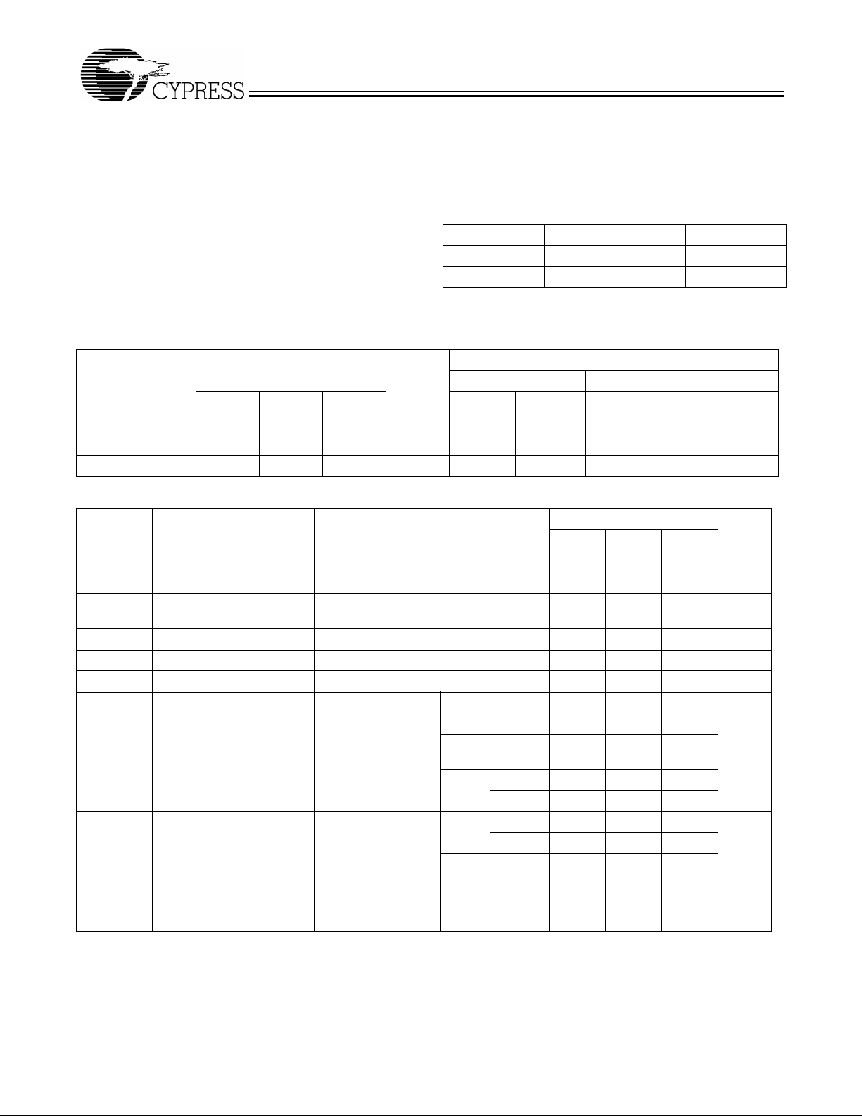
Maximum Ratings
(Abov e which the useful life may be impair ed. For user guidelines, not tested.)
Storage Temperature .................................–65°C to +150°C
Ambient Temperature with
Output Current into Outputs (LOW)............................. 20 mA
Static Discharge Voltage .......... ................................ >2001V
(per MIL-STD-883, Method 3015)
Latch-Up Current............. .......... .. .......... .. .......... .. ... >200 mA
Operating Range
Power Applied.............................................–55°C to +1 2 5 °C
Supply Voltage to Ground Potential
(Pin 28 to Pi n 14 ) ........ ... ............ ............ ........ –0.5V to +4.6V
DC Voltage Applied to Outputs
in High Z State
DC Input Voltage
[1]
....................................–0.5V to VCC + 0.5V
[1]
.................................–0.5V to VCC + 0.5V
Range Ambient Tem perature V
Commercial 0°C to +70°C 1.6V to 3.6V
Industrial –40°C to +85°C 1.6V to 3.6V
CC
Product Portfolio
Po wer Dissipation (Commercial)
VCC Range
Product Min. Typ.
[2]
Max. Speed Typ.
CY62128V 2.7V 3.0V 3.6V 55, 70 ns 20 mA 40 mA 0.4 µA 100 µA (XL = 10 µA)
CY62128V25 2.3V 2.5V 2.7V 100 ns 15 mA 20 mA 0.3 µA 50 µA (LL = 12 µA)
CY62128V18 1.6V 1.8V 2.0V 200 ns 10 mA 15 mA 0.3 µA 30 µA (LL = 10 µA)
Electrical Characteristics
Over the Operating Range
Parameter Description Test Conditions Min. Typ.
V
OH
V
OL
V
IH
V
IL
I
IX
I
OZ
I
CC
I
SB1
Notes:
1. V
IL
2. Typical values are included for reference only and are not guaranteed or tested. Typical values are measured at V
Output HIGH Volt age VCC = Min., IOH = –1.0 mA 2.4 V
Output LOW Voltage VCC = Min., IOL = 2.1 mA 0.4 V
Input HIG H Voltage 2 V
Input LOW Voltage –0.5 0.8 V
Input Load Current GND < VI < V
CC
Output Leakage Current GND < VO < VCC, Output Disabled –1 ±1 +1
VCC Operating Suppl y
Current
Auto matic CE
Power-Down Current—
TTL Inpu ts
(min.) = –2.0V for pulse durations of less than 20 ns.
VCC = Max.,
I
= 0 mA,
OUT
f = f
MAX
= 1/t
RC
Max. VCC, CE > VIH,
V
> VIH or
IN
V
< VIL, f = f
IN
MAX
Operating (ICC) Standby (I
[2]
Maximum Typ.
[2]
Maximum
CY62128V-55/70
[2]
Max. Unit
CC
+0.5V
–1 ±1 +1
Com’l,
70 ns
Ind’l,
L 20 40 mA
LL, XL 20 40
LL 23 50
55 ns
Ind’l,
70 ns
Com’l,
70 ns
Coml,
L 20 40
LL 20 40
L 15 300
LL, XL 15 300
LL 17 350
55 ns
Ind’l L 15 300
LL 15 300
= VCC Typ., TA = 25°C.
CC
SB2
)
V
µA
µA
µA
2
CY62128V Family
Electrical Characteristics
Over the Operating Range
CY62128V-55/70
Parameter Description Test Conditions Min. Typ.
I
SB2
Auto matic CE
Power-Down Current—
CMOS Inputs
Max. VCC,
CE
> VCC – 0.3V
V
> VCC – 0.3V
IN
or V
< 0.3V, f = 0
IN
Com’l L 0.4 100
LL 15
XL 10
Ind’l L 100
LL 30
Electrical Characteristics
Over the Operating Range
CY62128V25-100 CY62128V18-200
Parameter Description Test Conditions Min. Typ.
V
V
V
V
I
IX
I
OZ
I
CC
I
SB1
I
SB2
OH
OL
IH
IL
Output HIGH Volt age VCC = Min., IOH = –0.1 mA 2.4 0.8*
Output LOW Voltage VCC = Min., IOL = 0.1 mA 0.4 0.2 V
Input HIG H Voltage 2 V
Input LOW Voltage –0.5 0.8 –0.5 0.3*
Input Load Current GND < VI < V
CC
Output Leakage Current GND < VO < VCC, Output
–1 ±1 +1 –1 ±0.1 +1
–1 ±1 +1 –1 ±0.1 +1
Disabled
VCC Operating Suppl y
Current
Auto matic CE
Power-Down Current—
TTL Inpu ts
Auto matic CE
Power-Down Current—
CMOS Inputs
VCC = Max.,
I
= 0 mA,
OUT
f = f
MAX
= 1/t
RC
Max. VCC, CE > VIH,
V
> VIH or
IN
V
< VIL, f = f
IN
MAX
Max. VCC,
CE
> VCC – 0.3V
V
> VCC – 0.3V
IN
or V
< 0.3V, f = 0
IN
L 15 20 10 15 mA
LL
L 15 300 5 100
LL
L 0.4 50 0.4 30
LL 12 10
[2]
Max. Min. Typ.
CC
+0.5
V
0.7*
V
Indust’l Temp Range LL 24 20
Capacitance
[3]
CC
CC
[2]
Max. Unit
µA
µA
µA
µA
µA
[2]
Max. Unit
V
CC
+0.3
V
CC
V
V
V
µA
µA
µA
µA
µA
µA
Parameter Description Test Conditions Max. Unit
C
IN
C
OUT
Note:
3. Tested initially and after any design or process changes that may affect these parameters.
Input Capacitance TA = 25°C, f = 1 MHz,
V
= 3.0V
Output Capacitance 8 pF
CC
6 pF
3
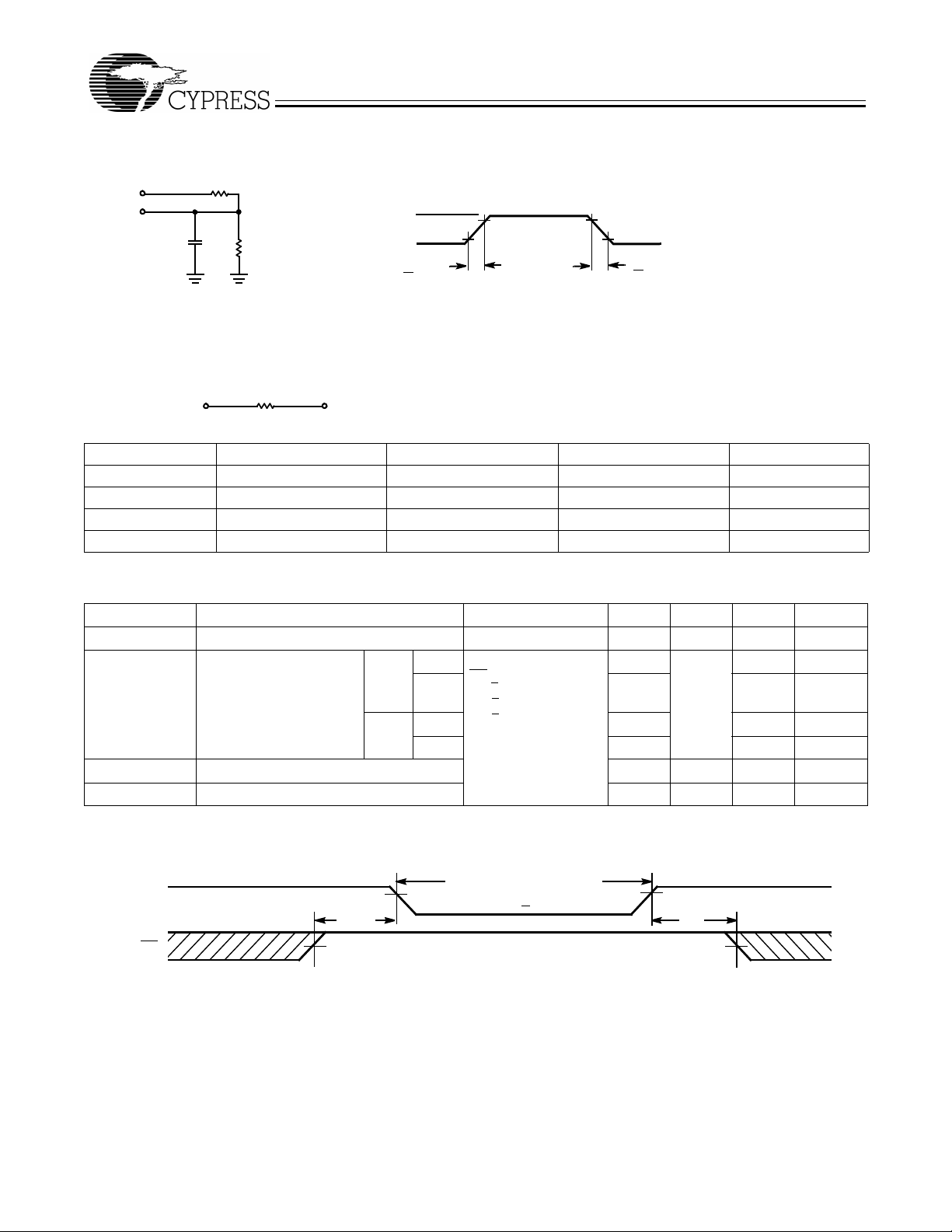
AC Test Loads and Waveforms
CY62128V Family
V
CC
OUTPUT
INCLUDING
JIG AND
Equivalent to: THÉ VENIN EQUIVALENT
R1
50 pF
SCOPE
OUTPUT V
R2
62128V–5
R
TH
1.8V
GND
<5ns
10%
ALL INPUT PULSES
90%
90%
10%
<5ns
62128V–6
Parameters 3.3V 2.5V 1.8V Unit
R1 1213 15909 10800 Ohms
R2 1378 4487 4154 Ohms
R
TH
V
TH
Data Rete n ti o n C h ar acteristics
Parameter Description Conditions
V
DR
I
CCDR
t
CDR
t
R
[3]
VCC for Da ta Rete ntion 1.6 V
Data Retention Current Com ’l L VCC = 2V
Chip Deselect to Data Retention Time 0 ns
Operation Recov ery Time t
645 3500 3000 Ohms
1.75V 0.55V 0.50V Volts
(Over the Operating Range)
[4]
Min. Typ.
[2]
0.4 10
CE
LL,
XL
Ind’l L 20
LL 20
> VCC – 0.3V,
V
> VCC – 0.3V or
IN
V
< 0.3V
IN
No input may exceed
V
+0.3V
CC
RC
Max. Unit
µA
10
µA
µA
µA
ns
Data Retention Waveform
V
CC
CE
Note:
4. No input may exceed V
CC
+0.3V.
t
CDR
DATA RETENTION MODE
VDR> 1.6 V
4
1.8V1.8V
t
R
C62128V–7

CY62128V Family
Data Retention Current Graph
Switching Characteristics
(for “L” version only)
DATA RETENTION
vs. SUPPLY VOLTAGE
80
70
A)
60
µ
(
50
40
30
20
10
SUPPLY CURRENT
0
1.6
SUPPLY VOLTAGE (V)
Over the Operating Range
CURRENT
T
=25°C
A
2.6
[5]
3.6
62128V-55 62128V-70 62128V25-100 62128V18-200
Parameter Description Min. Max. Min. Max. Min. Max. Min. Max. Unit
READ CYCLE
t
RC
t
AA
t
OHA
t
ACE
t
DOE
t
LZOE
t
HZOE
t
LZCE
t
HZCE
t
PU
t
PD
WRIT E CYCLE
t
WC
t
SCE
t
AW
t
HA
t
SA
t
PWE
t
SD
t
HD
t
HZWE
t
LZWE
5. Tes t conditions assume signal transition time of 5 ns or less timing reference levels of 1.5V , input pulse levels of 0 to 3.0V, and output loading of the specified
IOL/IOH and 100-pF load c apa citance .
6. At any given temperature and voltage condition, t
7. t
8. The internal write time of the memory is defined by the overlap of CE1 LOW , CE2 HIGH, and WE LOW . CE1 and WE signals must be LOW and CE2 HIGH to initiate a
9. The minimum write cycle time for write cycle #3 (WE
, t
HZCE
, and t
HZOE
write and either signal c an terminate a write by goin g HIGH. The data i nput set- up and hold timi ng should be r eferenc ed to the rising edge of the signal t hat terminates the write.
Read Cycle Time 55 70 100 200 ns
Address to Data Valid 55 70 100 200 ns
Data Hold from Address Change 5 10 10 10 ns
CE LOW to Data Valid 55 70 100 200 ns
OE LOW to Data Valid 20 35 75 125 ns
OE LOW to Low Z
OE HIGH to High Z
CE LOW to Low Z
CE HIGH to High Z
[6]
[6]
[6, 7]
[6, 7]
10 10 10 10 ns
20 25 50 75 ns
10 10 10 10 ns
20 25 50 75 ns
CE LOW to Po wer-Up 0 0 0 0 ns
CE HIGH to Power-Down 55 70 100 200 ns
[8, 9]
Write Cycle Time 55 70 100 200 ns
CE LOW to Write End 45 60 100 190 ns
Address Set-Up to Write End 45 60 100 190 ns
Address Hold from Write End 0 0 0 0 ns
Address Set-Up to Write Start 0 0 0 0 ns
WE Pu l s e W idth 45 55 90 125 ns
Data Set -U p to Write End 25 30 60 100 ns
Data Hold from Write End 0 0 0 0 ns
WE LOW to High Z
WE HIGH to Low Z
are specified with CL = 5 pF as in pa rt (b) of A C Test Loads. Transition is measured ±200 mV from s teady-st ate v oltage .
HZWE
[6, 7]
[6]
is less than t
HZCE
controlled, OE LOW) is the sum of t
5 5 10 15 ns
, t
LZCE
20 25 50 100 ns
HZOE
is less than t
HZWE
LZOE
and tSD.
, and t
HZWE
is less than t
for any given device.
LZWE
5

Switching Waveforms
CY62128V Family
Read Cycle No.1
[10, 11]
ADDRESS
t
OHA
DATA OUT PREVIOUS DATA VALID
Read Cycle No. 2 (OE Controll ed)
[11, 12]
ADDRESS
CE
1
CE
2
t
ACE
OE
t
t
LZCE
LZOE
50%
DATA OUT
V
CC
SUPPLY
HIGH IMPEDANCE
t
PU
CURRENT
Write Cycle No. 1 (CE1 or CE2 Controlled)
t
DOE
[13,14]
t
RC
t
AA
DATA VALID
62128V–8
t
RC
t
HZOE
t
DATA VALID
HZCE
t
PD
50%
HIGH
IMPEDANCE
62128V-9
I
CC
I
SB
ADDRESS
CE
1
CE
2
WE
DATA I/O
Notes:
10. Device is continuously selected. OE
11. WE
is HIGH for read cycle.
12. Address valid prior to or coincident with CE
13. Data I/O is high impedance if OE
14. If CE
goes HIGH or CE2 goes LOW si multane ously w ith WE HIGH, the output rem ains in a high- impedance st ate.
1
, CE = V
= VIH.
t
WC
t
SA
t
AW
IL, CE2=VIH
1
.
transition LOW and CE2 transition HIGH.
t
PWE
6
t
SCE
t
SCE
t
SD
DATA VALID
t
HA
t
HD
62128V-10

CY62128V Family
Switching Waveforms
Write Cycle No. 2 (WE Controlled, OE HIGH During Write)
(continued )
[13, 14]
t
WC
ADDRESS
t
SCE
CE
1
CE
2
t
SCE
t
AW
t
SA
WE
OE
DATA I/O
Note:
15. During this period, the I/Os are in output state and input signals should not be applied.
NOTE
15
t
HZOE
t
PWE
t
SD
DATAINVALID
t
HA
t
HD
62128V-11
Truth Table
CE
H X X X High Z Power-Down Standby (ISB)
X L X X High Z Power-Down Standby (ISB)
L H L H Data Out Read Active (ICC)
L H X L Data In Write Active (ICC)
L H H H Hi gh Z Selected, Outputs Disabled Active (ICC)
CE
1
OE WE I/O0–I/O
2
7
Mode Power
7

CY62128V Family
Ordering Information
Speed
(ns) Ordering Code
55 CY62128VLL-55ZAI ZA32 32-Lead STSOP Type 1 Industrial
70 CY62128VL-70SC S34 32-Lead 450-Mil SOIC Commercial
CY62128VLL-70SC S34
CY62128VL-70ZC Z32 32-Lead TSOP Type 1
CY62128VLL-70ZC Z32
CY62128VXL-70ZC Z32
CY62128VL-70ZAC ZA32 32-Lead STSOP Type 1
CY62128VLL-70ZAC ZA32
CY62128VL-70ZRC ZR32 32-Lead Reverse TSOP 1
CY62128VLL-70ZRC ZR32
70 CY62128VL-70SI S34 32-Lead 450-Mil SOIC Industrial
CY62128VLL-70SI S34
CY62128VL-70ZI Z32 32-Lead TSOP Type 1
CY62128VLL-70ZI Z32
CY62128VL-70ZAI ZA32 32-Lead STSOP Type 1
CY62128VLL-70ZAI ZA32
CY62128VL-70ZRI ZR32 32-Lead Reverse TSOP 1
CY62128VLL-70ZRI ZR32
100 CY62128V25L-100SC S34 32-Lead 450-Mil SOIC Commercial
CY62128V25LL-100SC S34
CY62128V25L-100ZC Z32 32-Lead TSOP Type 1
CY62128V25LL-100ZC Z32
CY62128V25L-100ZAC ZA32 32-Lead STSOP Type 1
CY62128V25LL-100ZAC ZA32
CY62128V25L-100ZRC ZR32 32-Lead Reverse TSOP 1
CY62128V25LL-100ZRC ZR32
100 CY62128V25L-100SI S34 32-Lead 450-Mil SOIC Industrial
CY62128V25LL-100SI S34
CY62128V25L-100ZI Z32 32-Lead TSOP Type 1
CY62128V25LL-100ZI Z32
CY62128V25L-100ZAI ZA32 32-Lead STSOP Type 1
CY62128V25LL-100ZAI ZA32
CY62128V25L-100ZRI ZR32 32-Lead Reverse TSOP 1
CY62128V25LL-100ZRI ZR32
200 CY62128V18L-200SC S34 32-Lead 450-Mil SOIC Commercial
CY62128V18LL-200SC S34
CY62128V18L-200ZC Z32 32-Lead TSOP Type 1
CY62128V18LL-200ZC Z32
CY62128V18L-200ZAC ZA32 32-Lead STSOP Type 1
CY62128V18LL-200ZAC ZA32
CY62128V18L-200ZRC ZR32 32-Lead Reverse TSOP 1
CY62128V18LL-200ZRC ZR32
Package
Name Package Type
Operating
Range
8

CY62128V Family
Ordering Information
Speed
(ns) Ordering Code
200 CY62128V18L-200SI S34 32-Lead 450-Mil SOIC Industrial
CY62128V18LL-200SI S34
CY62128V18L-200ZI Z32 32-Lead TSOP Type 1
CY62128V18LL-200ZI Z32
CY62128V18L-200ZAI ZA32 32-Lead STSOP Type 1
CY62128V18LL-200ZAI ZA32
CY62128V18L-200ZRI ZR32 32-Lead Reverse TSOP 1
CY62128V18LL-200ZRI ZR32
Document #: 38-00547-B
(continued)
Package
Name Package Type
Package Diagrams
32-Lead (450 MIL) Molded SOIC S34
Operating
Range
51-85081-A
9

CY62128V Family
Package Diagrams
(continued)
32-Lead Thin Small Outline Package Z32
51-85056-C
10

CY62128V Family
Package Diagrams
(continued)
32-Lead Shrunk Thin Small Outline Package ZA32
51-85094-B
11

CY62128V Family
Package Diagrams
(continued)
32-Lead Reverse Thin Small Outline Package ZR32
51-85089-B
© Cypress Semiconductor Corporation, 2000. The information contained herein is subject to change without notice. Cypress Semiconductor Corporation assumes no responsibility for the use
of any circuitry other than circuitry embodied in a Cypress Semiconductor product. Nor does it con vey or imply any lice nse under patent or other rights. Cypress Semicondu ctor does not authorize
its products for use as critical components in life-support systems where a malfunction or failure may reasonably be expected to result in significant injury to the user. The inclusion of Cypress
Semiconductor products in life-support systems application implies that the manufacturer assumes all risk of such use and in doing so indemnifies Cypress Semiconductor against all charges.
 Loading...