

Page 1
CY62128EV30
MoBL® 1 Mbit (128K x 8) Static RAM
Features
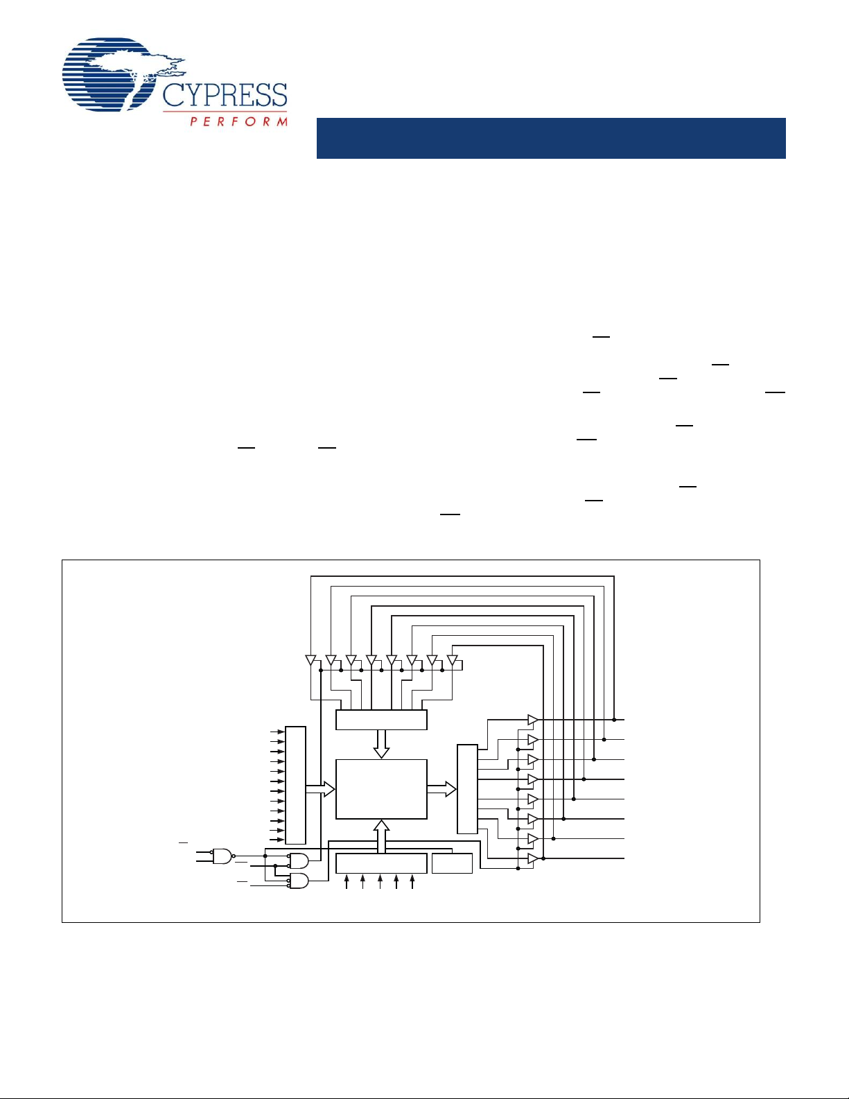
A
0
IO
0
IO
7
IO
1
IO
2
IO
3
IO
4
IO
5
IO
6
A
1
A
2
A
3
A
4
A
5
A
6
A
7
A
8
A
9
A
12
SENSE AMPS
POWER
DOWN
WE
OE
A
13
A
14
A15A
16
ROW DECODER
COLUMN DECODER
128K x 8
ARRAY
INPUT BUFFER
A
10
A
11
CE
1
CE
2
Logic Block Diagram
Note
1. For best practice recommendations, refer to the Cypress application note “System Design Guidelines” at http://www.cypress.com.
■ Very high speed: 45 ns
❐ Temperature ranges:
• Industrial: –40°C to +85°C
• Automotive-A: –40°C to +85°C
• Automotive-E: –40°C to +125°C
■ Wide voltage range: 2.20V – 3.60V
■ Pin compatible with CY62128DV30
■ Ultra low standby power
❐ Typical standby current: 1 μA
❐ Maximum standby current: 4 μA
■ Ultra low active power
❐ Typical active current: 1.3 mA @ f = 1 MHz
■ Easy memory expansion with CE
■ Automatic power down when deselected
■ CMOS for optimum speed and power
■ Offered in Pb-free 32-pin SOIC, 32-pin TSOP I, and 32-pin
STSOP packages
, CE2 and OE features
1
Functional Description
The CY62128EV30
module organized as 128K words by 8 bits. This device features
advanced circuit design to provide ultra low active current. This
is ideal for providing More Battery Life™ (MoBL
applications such as cellular telephones. The device also has an
automatic power down feature that significantly reduces power
consumption when addresses are not toggling. Placing the
device into standby mode reduces power consumption by more
than 99% when deselected (CE
input and output pins (IO
impedance state when the device is deselected (CE
CE
LOW), the outputs are disabled (OE HIGH), or a write
2
operation is in progress (CE
LOW).
To write to the device, take Chip Enable (CE
HIGH) and Write Enable (WE) inputs LOW. Data on the eight IO
pins is then written into the location specified on the Address pin
(A0 through A16).
To read from the device, take Chip Enable (CE1 LOW and CE
HIGH) and Output Enable (OE) LOW while forcing Write Enable
(WE
) HIGH. Under these conditions, the contents of the memory
location specified by the address pins appear on the IO pins.
[1]
is a high performance CMOS static RAM
®
) in portable
HIGH or CE2 LOW). The eight
1
through IO7) are placed in a high
0
LOW and CE2 HIGH and WE
1
1
HIGH or
1
LOW and CE
2
2
Cypress Semiconductor Corporation • 198 Champion Court • San Jose, CA 95134-1709 • 408-943-2600
Document #: 38-05579 Rev. *D Revised March 28, 2008
[+] Feedback
Page 2
CY62128EV30
A
6
A
7
A
16
A
14
A
12
WE
V
CC
A
4
A
13
A
8
A
9
OE
STSOP
Top View
(not to scale)
30
28
29
31
24
19
23
22
21
20
18
13
17
16
15
14
11
12
IO
2
IO
1
GND
IO
7
IO
4
IO
5
IO
6
IO
0
CE
1
A
11
A
5
9
10
32
1
2
3
4
5
6
7
8
CE
2
A
15
NC
A
10
IO
3
A
1
A
0
A
3
A
2
26
25
26
27
A
6
A
7
A
16
A
14
A
12
WE
V
CC
A
4
A
13
A
8
A
9
OE
TSOP I
Top View
(not to scale)
1
6
2
3
4
5
7
32
27
31
30
29
28
26
21
25
24
23
22
19
20
IO
2
IO
1
GND
IO
7
IO
4
IO
5
IO
6
IO
0
CE
1
A
11
A
5
17
18
8
9
10
11
12
13
14
15
16
CE
2
A
15
NC
A
10
IO
3
A
1
A
0
A
3
A
2
1
2
3
4
5
6
7
8
9
10
11
14
19
20
24
23
22
21
25
28
27
26
Top View
SOIC
12
13
29
32
31
30
16
15
17
18
GND
A
16
A
14
A
12
A
7
A
6
A
5
A
4
A
3
WE
V
CC
A
15
A
13
A
8
A
9
IO
7
IO
6
IO
5
IO
4
A
2
NC
IO
0
IO
1
IO
2
CE
1
OE
A
10
IO
3
A
1
A
0
A
11
CE
2
Notes
2. NC pins are not connected on the die.
3. Typical values are included for reference only and are not guaranteed or tested. Typical values are measured at V
CC
= V
CC(typ)
, TA = 25°C.
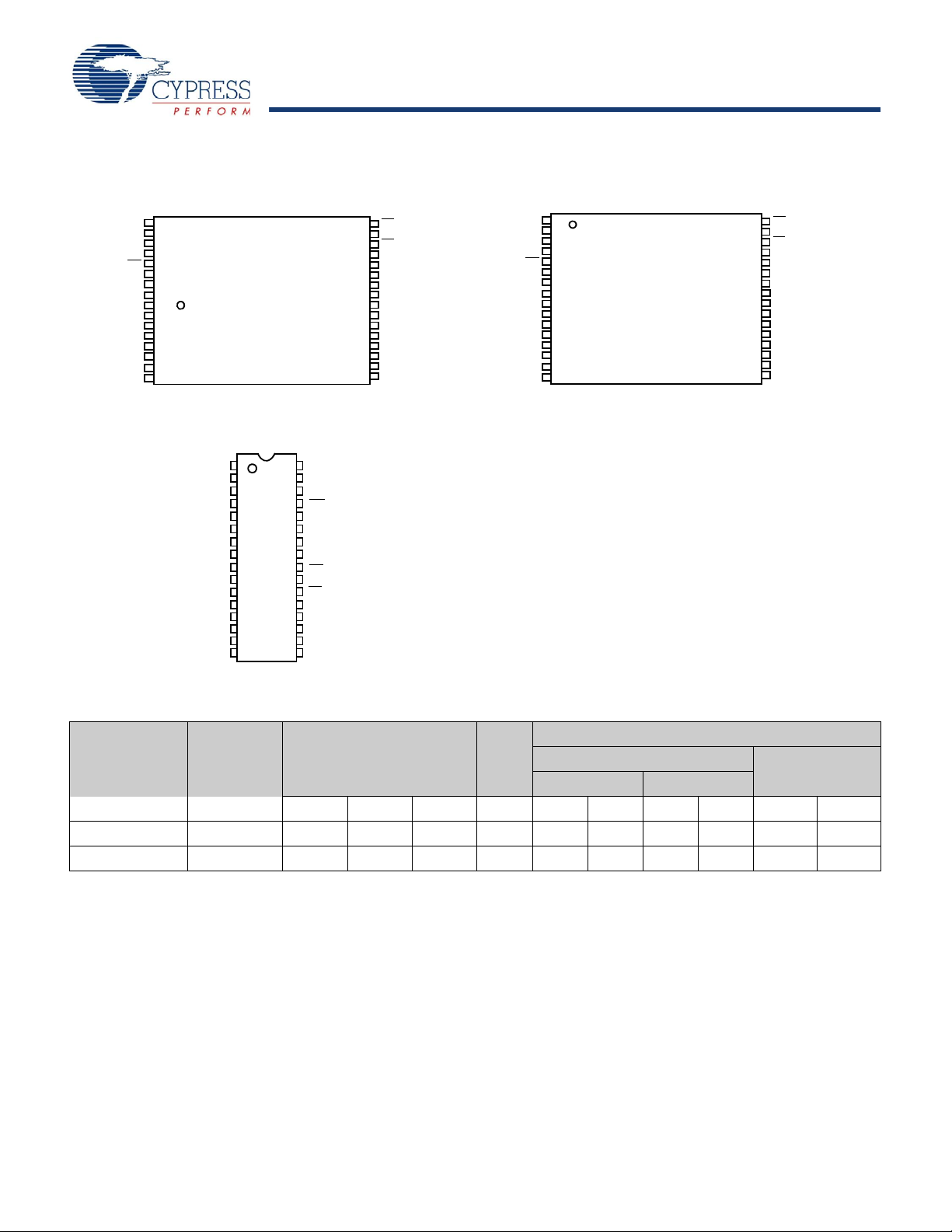
Pin Configuration
[2]
Table 1. Product Portfolio
Product Range VCC Range (V)
Min Typ
[3]
Max T yp
Speed
(ns)
CY62128EV30LL Ind’l/Auto-A 2.2 3.0 3.6 45 1.3 2.0 11 16 1 4
CY62128EV30LL Auto-E 2.2 3.0 3.6 55 1.3 4.0 11 35 1 30
Document #: 38-05579 Rev. *D Page 2 of 11
Power Dissipation
Operating ICC (mA)
f = 1 MHz f = f
[3]
Max Typ
[3]
max
Max Typ
Standby I
[3]
SB2
(µA)
Max
[+] Feedback
Page 3
CY62128EV30
Maximum Ratings
Notes
4. V
IL(min)
= –2.0V for pulse durations less than 20 ns.
5. V
IH(max)
= VCC+0.75V for pulse durations le ss th an 20 ns.
6. Full device AC operation assumes a 100 μs ramp time from 0 to V
CC
(min) and 200 μs wait time after V
CC
stabilization.
7. Only chip enables (CE
1
and CE2) must be at CMOS level to meet the I
SB2
/ I
CCDR
spec. Other inputs can be left floating.
Exceeding maximum ratings may impair the useful life of the
device. These user guidelines are not tested.
Storage Temperature.................................. –65°C to +150°C
Ambient Temperature with
Power Applied ............................................–55°C to +125°C
Supply Voltage to Ground
Potential..........................................–0.3V to V
DC Voltage Applied to Outputs
in High-Z State
DC Input Voltage
[4, 5]
.........................–0.3V to V
[4,5]
.......................–0.3V to V
CC(max)
CC(max)
CC(max)
+ 0.3V
+ 0.3V
+ 0.3V
Electrical Characteristics
(Over the Operating Range)
Output Current into Outputs (LOW).............................20 mA
Static Discharge Voltage.......................................... > 2001V
(MIL-STD-883, Method 3015)
Latch up Current.....................................................> 200 mA
Operating Range
Device Range
CY62128EV30LL Ind’l/Auto-A –40°C to +85°C 2.2V to
Auto-E –40°C to +125°C
Ambient
Temperature
V
CC
3.6V
[6]
Parameter Description Test Conditions
V
OH
V
OL
V
IH
V
IL
Output HIGH Voltage IOH = –0.1 mA 2.0 2.0 V
IOH = –1.0 mA, V
CC
> 2.70V
Output LOW Voltage IOL = 0.1 mA 0.4 0.4 V
Input HIGH Voltage V
Input LOW Voltage V
IOL = 2.1 mA, V
= 2.2V to 2.7V 1.8 V
CC
V
= 2.7V to 3.6V 2.2 V
CC
= 2.2V to 2.7V –0.3 0.6 –0.3 0.6 V
CC
> 2.70V 0.4 0.4 V
CC
VCC= 2.7V to 3.6V –0.3 0.8 –0.3 0.8 V
I
IX
I
OZ
I
CC
I
SB1
I
SB2
[7]
Input Leakage Current GND < VI < V
CC
Output Leakage Current GND < VO < VCC, Output Disabled –1 +1 –4 +4 μA
VCC Operating Supply
Current
Automatic CE
Power down
Current — CMOS Inputs
Automatic CE
Power down
Current — CMOS Inputs
f = f
= 1/t
max
RCVCC
f = 1 MHz 1.3 2.0 1.3 4.0 mA
CE
> VCC−0.2V, CE2 < 0.2V
1
V
> VCC–0.2V, V
IN
f = f
f = 0 (OE
(Address and Data Only),
max
and WE), V
= V
I
= 0 mA
OUT
CMOS levels
< 0.2V)
IN
CC
CE1 > VCC – 0.2V, CE2 < 0.2V
V
> VCC – 0.2V or VIN < 0.2V,
IN
f = 0, V
= 3.60V
CC
CCmax
= 3.60V
45 ns (Ind’l/Auto-A) 55 ns (Auto-E)
Min Typ
[3]
Max Min Typ
[3]
Max
2.4 2.4 V
+
CC
0.3V
CC
0.3V
1.8 V
+
2.2 V
CC
0.3V
CC
0.3V
+
+
–1 +1 –4 +4 μA
11 16 11 35 mA
14 135μA
14 130μA
Unit
V
V
Document #: 38-05579 Rev. *D Page 3 of 11
[+] Feedback
Page 4
CY62128EV30
Capacitance
Note
8. Teste d initially and after any design or process changes that may affect these parameters.
9. Full device AC operation requires linear V
CC
ramp from V
DR
to V
CC(min)
> 100 μs or stable at V
CC(min)
> 100 μs.
V
CC
V
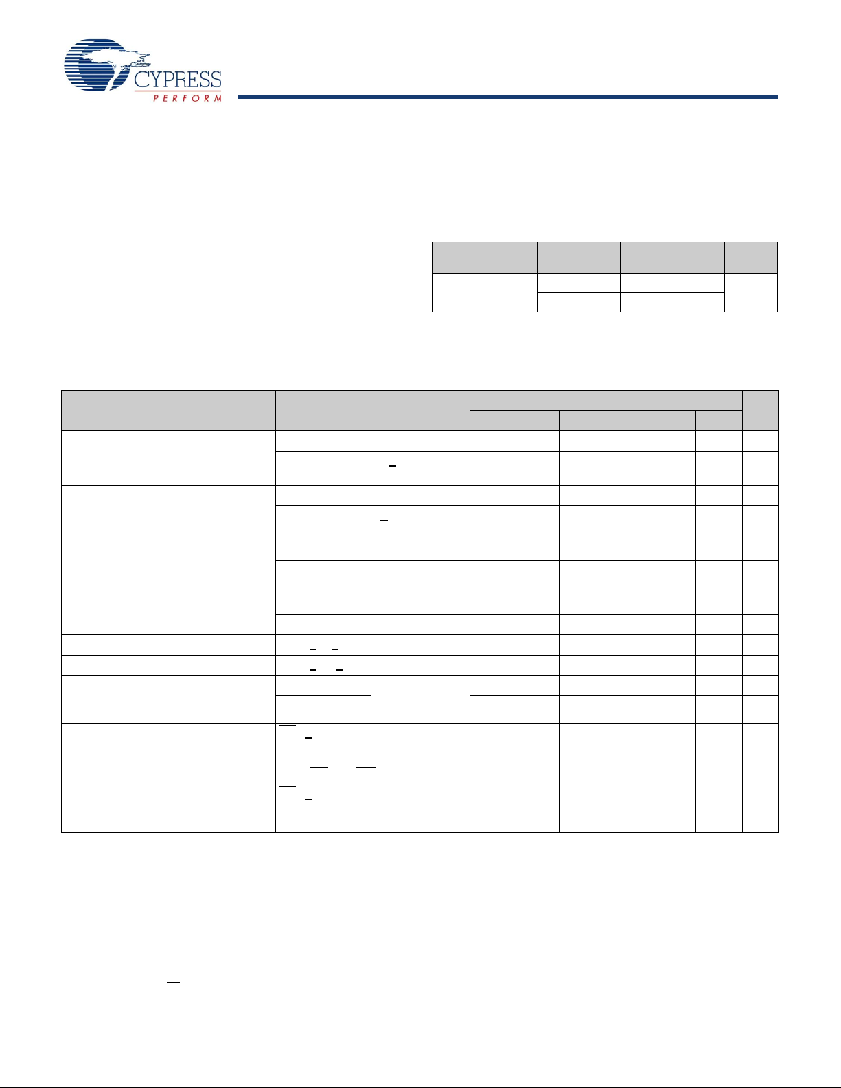
CC
OUTPUT
R2
30 pF
INCLUDING
JIG AND
SCOPE
GND
90%
10%
90%
10%
Rise Time = 1 V/ns
Fall Time = 1 V/ns
OUTPUT V
Equivalentto: THEVENIN EQUIVALENT
ALL INPUT PULSES
R
TH
R1
(For all packages)
Parameter Description Test Conditions Max Unit
C
IN
C
OUT
[8]
Input Capacitance TA = 25°C, f = 1 MHz,
V
= V
CC
Output Capacitance 10 pF
CC(typ)
10 pF
Thermal Resistance
Parameter Description Test Conditions TSOP I SOIC STSOP Unit
Θ
JA
Θ
JC
Thermal Resistance
(Junction to Ambient)
Thermal Resistance
(Junction to Case)
Still Air, soldered on a 3 x 4.5 inch,
two-layer printed circuit board
Figure 1. AC Test Loads and Waveforms
33.01 48.67 32.56 °C/W
3.42 25.86 3.59 °C/W
Parameters 2.50V 3.0V Unit
R1 16667 1103 Ω
R2 15385 1554 Ω
R
TH
V
TH
8000 645 Ω
1.20 1.75 V
Data Retention Characteristics
(Over the Operating Range)
Parameter Description Conditions Min Typ
V
DR
I
CCDR
t
CDR
[9]
t
R
[7]
[8]
VCC for Data Retention 1.5 V
Data Retention Current VCC = 1.5V,
CE
> VCC − 0.2V or CE2 < 0.2V,
1
V
> VCC − 0.2V or VIN < 0.2V
IN
Ind’l/Auto-A 3 μA
Auto-E 30 μA
Chip Deselect to Data Retention
Time
Operation Recovery Time t
[3]
Max Unit
0ns
RC
ns
Document #: 38-05579 Rev. *D Page 4 of 11
[+] Feedback
Page 5

CY62128EV30
Data Retention Waveform
V
CC(min)
V
CC(min)
t
CDR
VDR> 1.5V
DATA RETENTION MODE
t
R
V
CC
CE
Notes
10.CE
is the logical combination of CE1 and CE2. When CE1 is LOW and CE2 is HIGH, CE is LOW; when CE1 is HIGH or CE2 is LOW, CE is HIGH.
11.Test Conditions for all parameters other than tri-st ate parameters assume si gnal transition time of 3 ns or less (1 V/ns), timing reference levels of V
CC(typ)
/2, input
pulse levels of 0 to V
CC(typ)
, and output loading of the specified IOL/IOH as shown in the “AC Test Loads and Waveforms” on page 4.
12.At any given temperature and voltage condition, t
HZCE
is less than t
LZCE
, t
HZOE
is less than t
LZOE
, and t
HZWE
is less than t
LZWE
for any given device.
13.t
HZOE
, t
HZCE
, and t
HZWE
transitions are measured when the output enter a high impedance state.
14.The internal write time of the memory is defined by the overlap of WE
, CE = VIL. All signals must be ACTIVE to initiate a write and any of these signals can
terminate a write by going INACTIVE. The data input setup and hold timing should be referenced to the edge of the signal that terminates the write.
[10]
Switching Characteristics
(Over the Operating Range)
Parameter Description
Read Cycle
t
RC
t
AA
t
OHA
t
ACE
t
DOE
t
LZOE
t
HZOE
t
LZCE
t
HZCE
t
PU
t
PD
Write Cycle
t
WC
t
SCE
t
AW
t
HA
t
SA
t
PWE
t
SD
t
HD
t
HZWE
t
LZWE
[14]
[10, 11]
Read Cycle Time 45 55 ns
Address to Data Valid 45 55 ns
Data Hold from Address Change 10 10 ns
CE LOW to Data Valid 45 55 ns
OE LOW to Data Valid 22 25 ns
OE LOW to Low Z
OE HIGH to High Z
CE
LOW to Low Z
CE HIGH to High Z
CE LOW to Power Up
CE HIGH to Power Up 45 55 ns
Write Cycle Time 45 55 ns
CE LOW to Write End 35 40 ns
Address Setup to Write End 35 40 ns
Address Hold from Write End 0 0 ns
Address Setup to Write Start 0 0 ns
WE Pulse Width
Data Setup to Write End 25 25 ns
Data Hold from Write End 0 0 ns
WE LOW to High Z
WE HIGH to Low Z
[12]
[12,13]
[12]
[12, 13]
[12, 13]
[12]
45 ns (Ind’l/Auto-A) 55 ns (Auto-E)
Min Max Min Max
Unit
55ns
18 20 ns
10 10 ns
18 20 ns
00ns
35 40 ns
18 20 ns
10 10 ns
Document #: 38-05579 Rev. *D Page 5 of 11
[+] Feedback
Page 6

CY62128EV30
Switching Waveforms
PREVIOUS DATA VALID DATA VALID
RC
t
AA
t
OHA
tRC
ADDRESS
DATA OUT
50%
50%
DATA VALID
t
RC
t
ACE
t
DOE
t
LZOE
t
LZCE
t
PU
HIGH IMPEDANCE
t
HZOE
t
HZCE
t
PD
IMPEDANCE
I
CC
I
SB
HIGH
ADDRESS
CE
DATA OUT
V
CC
SUPPLY
CURRENT
OE
DATA VALID
t
HD
t
SD
t
PWE
t
SA
t
HA
t
AW
t
SCE
t
WC
t
HZOE
ADDRESS
CE
WE
DATA IO
OE
NOTE
20
Notes
15.The device is continuously selected. OE
, CE1 = VIL, CE2 = VIH.
16.WE
is HIGH for read cycle.
17.Address valid before or similar to CE
1
transition LOW and CE2 transition HIGH.
18.Data IO is high impedance if OE
= VIH.
19.If CE
1
goes HIGH or CE2 goes LOW simultaneously with WE HIGH, the output remains in high impedance state.
20.During this period, the IOs are in output state. Do not apply input signals.
Figure 2. Read Cycle 1 (Address transition controlled)
[15, 16]
Figure 3. Read Cycle No. 2 (OE controlled)
Figure 4. Write Cycle No. 1 (WE controlled)
[10, 16, 17]
[10, 15, 18, 19]
Document #: 38-05579 Rev. *D Page 6 of 11
[+] Feedback
Page 7

CY62128EV30
Switching Waveforms (continued)
t
WC
DATA VALID
t
AW
t
SA
t
PWE
t
HA
t
HD
t
SD
t
SCE
ADDRESS
CE
DATA IO
WE
DATA VALID
t
HD
t
SD
t
LZWE
t
PWE
t
SA
t
HA
t
AW
t
SCE
t
WC
t
HZWE
ADDRESS
CE
WE
DATA IO
NOTE
20
Figure 5. Write Cycle No. 2 (CE1 or CE2 controlled)
[10, 14, 18, 19]
Figure 6. Write Cycle No. 3 (WE controlled, OE LOW)
[10, 19]
Table 2. Truth Table for CY62128EV30
CE1CE
H X X X High Z Deselect/Power Down Standby (I
WE OE Inputs/Outputs Mode Power
2
SB
)
X L X X High Z Deselect/Power Down Standby (ISB)
)
CC
)
CC
)
CC
L H H L Data Out Read Active (I
L H H H High Z Output Disabled Active (I
L H L X Data in Write Active (I
Document #: 38-05579 Rev. *D Page 7 of 11
[+] Feedback
Page 8

CY62128EV30
Ordering Information
0.546[13.868]
0.440[11.176]
0.101[2.565]
0.050[1.270]
0.014[0.355]
0.118[2.997]
0.004[0.102]
0.047[1.193]
0.006[0.152]
0.023[0.584]
0.793[20.142]
0.450[11.430]
0.566[14.376]
0.111[2.819]
0.817[20.751]
BSC.
0.020[0.508]
MIN.
MAX.
0.012[0.304]
0.039[0.990]
0.063[1.600]
SEATING PLANE
116
17 32
0.004[0.102]
51-85081-*B
Speed
(ns)
Ordering Code
45 CY62128EV30LL-45SXI 51-85081 32-pin 450-Mil SOIC (Pb-free) Industrial
CY62128EV30LL-45ZXI 51-85056 32-pin TSOP Type I (Pb-free)
CY62128EV30LL-45ZAXI 51-85094 32-pin STSOP (Pb-free)
45 CY62128EV30LL-45ZXA 51-85056 32-pin TSOP Type I (Pb-free) Automotive-A
55 CY62128EV30LL-55ZXE 51-85056 32-pin TSOP Type I (Pb-free) Automotive-E
Contact your local Cypress sales representative for availability of these parts.
Package
Diagram
Package Type
Package Diagrams
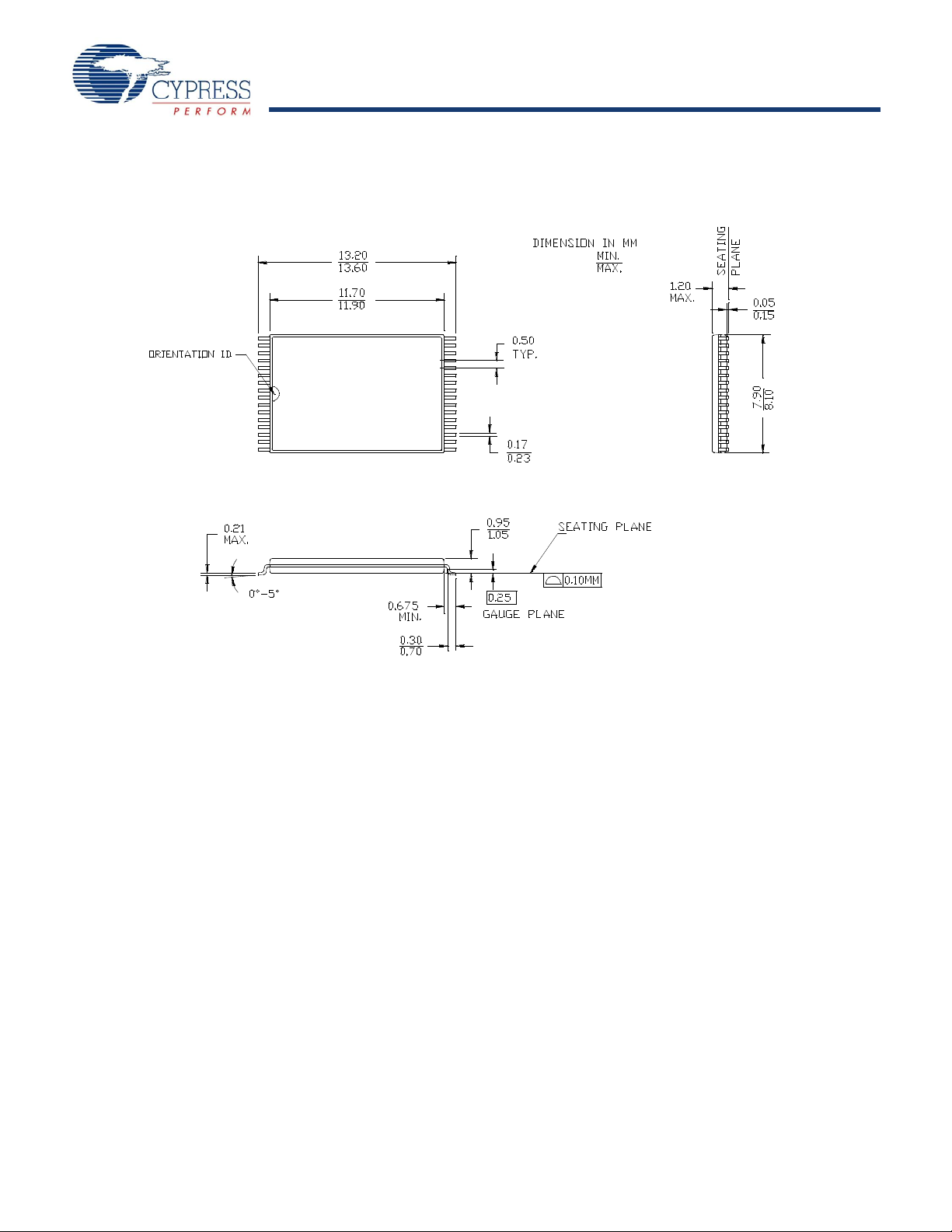
Figure 7. 32-Pin (450 Mil) Molded SOIC, 51-85081
Operating
Range
Document #: 38-05579 Rev. *D Page 8 of 11
[+] Feedback
Page 9

CY62128EV30
Package Diagrams (continued)
51-85056-*D
Figure 8. 32-Pin Thin Small Outline Package Type I (8 x 20 mm), 51-85056
Document #: 38-05579 Rev. *D Page 9 of 11
[+] Feedback
Page 10
CY62128EV30
Package Diagrams (continued)
51-85094-*D
Figure 9. 32-Pin Shrunk Thin Small Outline Package (8 x 13.4 mm), 51-85094
Document #: 38-05579 Rev. *D Page 10 of 11
[+] Feedback
Page 11

CY62128EV30
Document History Page
Document Title: CY62128EV30 MoBL® 1 Mbit (128K x 8) Static RAM
Document Number: 38-05579
REV. ECN NO. Issue Date Orig. of
Change
** 285473 See ECN PCI New Data Sheet
*A 461631 See ECN NXR Converted from Preliminary to Final
Removed 35 ns Speed Bin
Removed “L” version of CY62128EV30
Removed Reverse TSOP I package from Product offering.
Changed I
Changed I
Changed I
Changed I
Changed I
Changed the AC Test load Capacitance value from 50 pF to 30 pF
Changed t
Changed t
Changed t
Changed t
Changed t
Changed t
Updated the Ordering Information table.
from 8 mA to 11 mA and I
CC (Typ)
CC (max)
SB2 (max)
SB2 (Typ)
CCDR (max)
LZOE
LZCE
HZCE
PWE
SD
LZWE
from 1.5 mA to 2.0 mA for f = 1 MHz
from 1 μA to 4 μA
from 0.5 μA to 1 μA
from 3 to 5 ns
from 6 to 10 ns
from 22 to 18 ns
from 30 to 35 ns
from 22 to 25 ns
from 6 to 10 ns
*B 464721 See ECN NXR Updated the Block Diagram on page # 1
*C 1024520 See ECN VKN Added final Automotive-A and Automotive-E information
Added footnote #9 related to I
Updated Ordering Information table
*D 2257446 See ECN NXR Changed the Maximum rating of Ambient Temperature with Power Applied from
55°C to +125°C to –55°C to +125°C.
Description of Change
from 1 μA to 3 μA
and I
SB2
CC (Max)
CCDR
from 12 mA to 16 mA for f = f
max
© Cypress Semiconductor Corporation, 2004- 2008. The infor mation cont ain ed herein is subj ect to change wi thout notice. C ypress Semiconductor Corporation assumes no responsibility for the use of
any circuitry other than circuitry embodied in a Cypress product. Nor does it convey or imply any license under patent or other rights. Cypress products are not war ran ted no r inte nd ed to be us ed fo r
medical, life support, life saving, critica l contr o l or safety applications, unless pursuant to an express written ag re em en t w it h C ypr ess. Fu rth erm ore, Cyp ress doe s not auth ori ze i t s pr o ducts for use as
critical components in life-support systems where a malfunction or fa ilure may reasonably be expe cted to result in significa nt injury to the us er . The inclu sion of Cypress p roducts in life -support systems
application implies that the manufacturer assumes all risk of such use and in doing so indemnifies Cypress against all charges.
Any Source Code (software and/or firmware) is owned by Cypress Semiconductor Corporation (Cypress) and is protected by and subject to worldwide patent protection (United States and foreign),
United States copyright laws and international treaty provisions. Cypress hereby gr ant s to l icense e a pers onal, no n-exclu sive , non-tr ansfer able license to copy, use, modify , cr eate der ivative works of ,
and compile the Cypress Source Code and derivative works for the sole purpose of creating custom software and or firmware in support of licensee product to be used only in conjuncti on with a Cypress
integrated circuit as specified in the ap plicable agreem ent. Any reprod uction, modificatio n, translation, co mpilation, or repr esentation of this Source Co de except as speci fied above is pro hibited with out
the express written permission of Cypress.
Disclaimer: CYPRESS MAKES NO WARRANTY OF ANY KIND, EXPRESS OR IMPLIED, WITH REGARD TO THIS MATERIAL, INCLUDING, BUT NOT LIMITED TO, THE IMPLIED WARRANTIES
OF MERCHANTABILITY AND FITNESS FOR A PARTICULAR PURPOSE. Cypress reserves the right to make changes without further notice to the materials described herei n. Cypress doe s not
assume any liability arising out of the applic ation or use o f any pr oduct or circ uit de scribed herein . Cypr ess does n ot author ize its p roducts fo r use as critical compon ents in life-su pport systems whe re
a malfunction or failure may reason ably be expected to result in significant injury to the user. The inclusion of Cypress’ product in a life-support systems application implies that the manufacturer
assumes all risk of such use and in doing so indemnifies Cypress against all charges.
Use may be limited by and subject to the applicable Cypress software license agreement.
Document #: 38-05579 Rev. *D Revised March 28, 2008 Page 11 of 11
MoBL is a registered trademark, and More Battery Life is a trademark, of Cypress Semiconductor. All other trademarks or registered trademarks referenced herein are property of the respective
corporations. All products and company names mentioned in this document may be the trademarks of their respective holders.
[+] Feedback
 Loading...