

Page 1
MoBL
®
1-Mbit (128K x 8) Static RAM
CY62128B
Features
• Temperature Ranges
—Commercial: 0°C to 70°C
—Industrial: –40°C to 85°C
—Automotive: –40°C to 125°C
• 4.5V–5.5V operation
• CMOS for optimum speed/power
• Low active power
(70 ns, LL version, Commercial, Industrial)
—82.5 mW (max.) (15 mA)
• Low standby power
(70 ns, LL version, Commercial, Industrial)
—110 µW (max.) (15 µA)
• Automatic power-down when deselected
• TTL-compatible inputs and outputs
• Easy memory expansion with CE
, CE2, and OE options
1
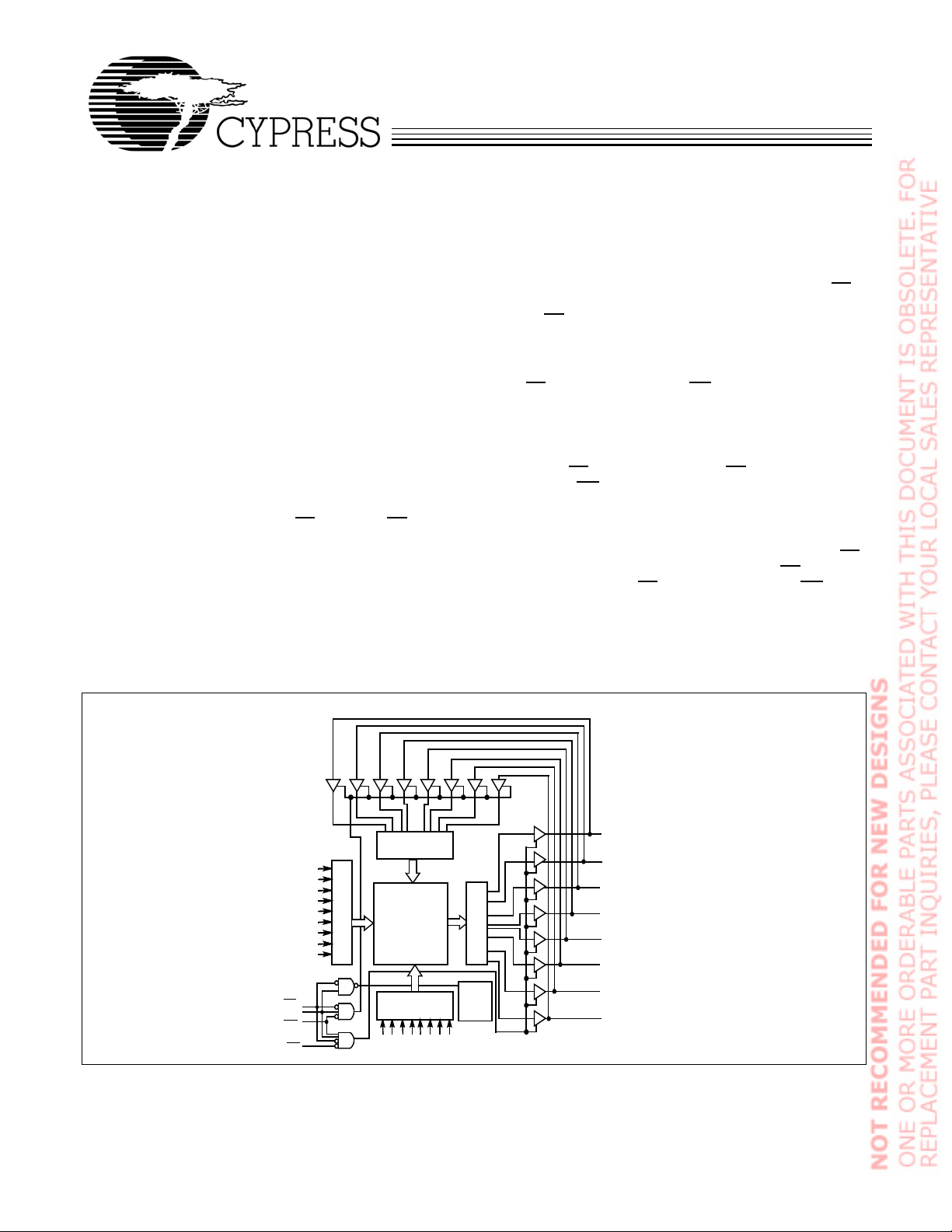
Functional Description
[1]
The CY62128B is a high-performance CMOS static RAM
organized as 131,072 words by 8 bits. Easy memory
expansion is provided by an active LOW Chip Enable (CE1),
an active HIGH Chip Enable (CE
Enable (OE
), and three-state drivers. This device has an
), an active LOW Output
2
automatic power-down feature that reduces power
consumption by more than 75% when deselected.
Writing to the device is accomplished by taking Chip Enable
One (CE
Enable Tw o (CE
through I/O7) is then written into the location specified on the
address pins (A
) and Write Enable (WE) inputs LOW and Chip
1
) input HIGH. Data on the eight I/O pins (I/O
2
through A16).
0
Reading from the device is accomplished by taking Chip
Enable One (CE
Write Enable (WE
) and Output Enable (OE) LOW while forcing
1
) and Chip Enable Two (CE2) HIGH. Under
these conditions, the contents of the memory location
specified by the address pins will appear on the I/O pins.
The eight input/output pins (I/O
high-impedance state when the device is deselected (CE
through I/O7) are placed in a
0
HIGH or CE2 LOW), the outputs are disabled (OE HIGH), or
during a write operation (CE
LOW, CE2 HIGH, and WE LOW).
1
The CY62128B is available in a standard 450-mil-wide SOIC,
32-pin TSOP type I and STSOP packages.
0
1
Logic Block Diagram
I/O
INPUT BUFFER
A
0
A
1
A
2
A
3
A
4
A
5
A
6
A
7
A
8
CE
1
CE
2
WE
OE
Note:
1. For best-practice recommendations, please refer to the Cypress application note “System Design Guidelines” on http://www.cypress.com.
512x256x8
ROW DECODER
ARRAY
COLUMN
DECODER
10
9
A
A
SENSE AMPS
POWER
DOWN
11
14
15
16
12
A
A
A
A
A13A
0
I/O
1
I/O
2
I/O
3
I/O
4
I/O
5
I/O
6
I/O
7
Cypress Semiconductor Corporation • 3901 North First Street • San Jose, CA 95134 • 408-943-2600
Document #: 38-05300 Rev. *C Revised March 7, 2005
[+] Feedback
Page 2
CY62128B
MoBL
Product Portfolio
Power Dissipation
V
Product
Range (V)
CC
Min. T yp.
[2]
Max. T y p.
Speed
(ns)
(mA)
[2]
Max. Typ.
CY62128BLL Industrial 4.5 5.0 5.5 55 7.5 20 2.5 15
Industrial 70 6 15 2.5 15
Automotive 70 6 25 2.5 25
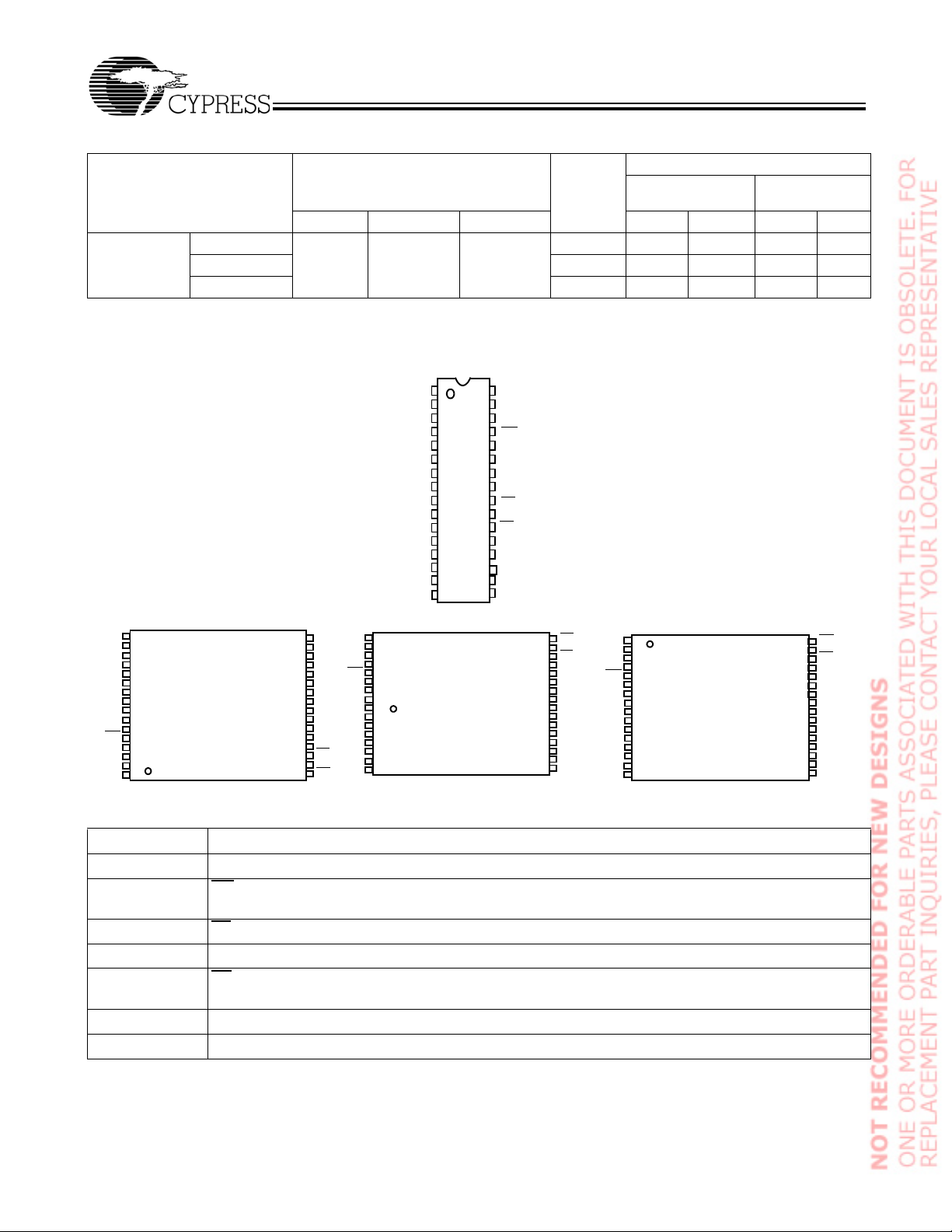
Pin Configurations
Top View
SOIC
Operating, ICC
NC
A
16
A
14
A
12
A
A
A
A
A
A
A
A
I/O
I/O
I/O
GN
gncGg
GND
7
6
5
4
3
2
1
12
0
0
13
1
14
2
151718
16
1
2
3
4
5
6
7
8
9
10
11
V
32
CC
31
A
15
30
CE
2
29
WE
28
A
13
27
A
8
26
A
9
25
A
11
24
OE
23
A
10
22
CE
1
I/O
21
7
I/O
6
20
I/O
5
19
I/O
4
I/O
3
Standby, I
(µA)
[2]
Max.
SB2
®
A
4
16
A
5
15
A
14
6
A
13
7
A
12
12
A
11
14
A
16
NC
V
CC
A
15
CE
2
WE
A
13
A
8
A
9
A
11
10
9
8
7
6
5
4
3
2
1
Reverse TSOP I
Top View
(not to scale)
A
A
CE
V
A
WE
A
NC
A
A
A
25
11
26
A
9
27
A
8
28
13
29
30
2
31
15
32
CC
1
2
16
3
14
4
12
A
5
7
A
6
6
7
A
5
8
A
4
STSOP
Top View
(not to scale)
24
OE
A
1
23
A
22
CE
21
I/O
20
I/O
19
I/O
18
I/O
17
I/O
16
GND
I/O
15
14
I/O
I/O
13
A
12
A
11
10
A
A
9
11
2
A
10
0
1
2
3
9
3
A
1
8
4
A
7
13
CE
V
WE
A
NC
A
A
A
5
6
2
7
15
8
CC
9
10
16
11
14
12
12
A
13
7
A
14
6
15
A
5
16
A
4
TSOP I
Top View
(not to scale)
6
5
4
3
2
1
0
32
OE
31
A
10
30
CE
29
I/O
28
I/O
27
I/O
26
I/O
25
25
I/O
24
GND
I/O
23
22
I/O
I/O
21
A
20
0
A
19
1
18
A
2
A
17
3
17
3
A
18
2
A
19
1
A
20
0
I/O
21
0
I/O
22
1
I/O
23
2
GND
24
I/O
3
25
I/O
4
26
I/O
27
5
I/O
6
28
I/O
7
29
CE
1
30
A
10
31
OE
32
Pin Definitions
Input A0-A16. Address Inputs
Input/Output I/O
Input/Control WE
Input/Control CE
Input/Control CE
Input/Control OE
Ground GND. Ground for the device
Power Supply V
Note:
2. Typical values are included for reference only and are not tested or guaranteed. Typical values are an averag e of the distribution across normal production
variations as measured at V
-I/O7. Data lines. Used as input or output lines depending on operation
0
. Write Enable, Active LOW. When selected LOW , a WRITE is conducted. When selected HIGH, a READ
is conducted.
. Chip Enable 1, Active LOW.
1
. Chip Enable 2, Active HIGH.
2
. Output Enable, Active LOW. Controls the direction of the I/O pins. When LOW, the I/O pins behave as
outputs. When deasserted HIGH, I/O pins are three-stated, and act as input data pins
. Power supply for the device
CC
= 5.0V, TA = 25°C, and t
CC
AA
= 70 ns.
1
7
6
5
4
3
2
1
0
Document #: 38-05300 Rev. *C Page 2 of 11
[+] Feedback
Page 3
CY62128B
MoBL
®
Maximum Ratings
(Above which the useful life may be impaired. For user guidelines, not tested.)
Storage Temperature .................................–65°C to +150°C
Ambient Temperature with
Current into Outputs (LOW).........................................20 mA
Static Discharge Voltage...........................................> 2001V
(per MIL-STD-883, Method 3015)
Latch-up Current.....................................................> 200 mA
Operating Range
Power Applied.................................. ... ........–55°C to +125°C
Supply Voltage on V
DC Voltage Applied to Outputs
in High-Z State
[3]
DC Input Voltage
to Relative GND
CC
................................. .. .–0.5V to V
[3]
.................................–0.5V to VCC + 0.5V
[3]
....–0.5V to +7.0V
CC
+ 0.5V
Range
Commercial 0°C to +70°C 5V ± 10%
Industrial –40°C to +85°C5V ± 10%
Automotive –40°C to +125°C5V ± 10%
Electrical Characteristics Over the Operating Range
CY62128B-55 CY62128B-70
Parameter Description T est Conditions
V
OH
V
OL
V
IH
V
IL
I
IX
Output HIGH Voltage VCC = Min., IOH = –1.0 mA 2.4 2.4 V
Output LOW Voltage VCC = Min., IOL = 2.1 mA 0.4 0.4 V
Input HIGH Voltage 2.2 V
Input LOW Voltage
Input Load Current GND ≤ VI ≤ V
[3]
CC
Min. Typ.
–0.3 0.8 –0.3 0.8 V
–1 +1 –1 +1 µA
Automotive
I
OZ
I
OS
I
CC
I
SB1
I
SB2
Notes:
3. V
IL
4. T
is the “Instant On” case temperature.
A
5. Not more than one output should be shorted at one time. Duration of the short circuit should not exceed 30 seconds.
Output Leakage
Current
Output Short Circuit
[5]
Current
VCC Operating
Supply Current
Automatic CE
Power-down Current
—TTL Inputs
Automatic CE
Power-down Current
—CMOS Inputs
(min.) = –2.0V for pulse durations of less than 20 ns.
GND ≤ VI ≤ VCC,
Output Disabled
VCC = Max., V
VCC = Max.,
= 0 mA,
I
OUT
f = f
MAX
= 1/t
Max. VCC,
CE
≥ V
1
or CE2 < VIL,
V
≥ VIH or
IN
V
≤ VIL, f = f
IN
Max. VCC,
CE
≥ VCC – 0.3V,
1
≤ 0.3V,
or CE
2
V
≥ VCC – 0.3V,
IN
or V
≤ 0.3V, f = 0
IN
–1 +1 –1 +1 µA
Automotive
= GND –300 –300 mA
OUT
Industrial,
Commercial
RC
Automotive
Industrial
IH
Commercial
Automotive
MAX
Industrial
Commercial
Automotive
[2]
7.5 20 6 15 mA
0.1 20.11mA
2.5 15 2.5 15 µA
Ambient
Temperature (TA)
Max. Min. Typ.
2.2 V
CC
+ 0.3
–10 +10 µA
–10 +10 µA
[4]
[2]
Max.
CC
+ 0.3
V
CC
Unit
V
625mA
0.1 2 mA
2.5 25 µA
Document #: 38-05300 Rev. *C Page 3 of 11
[+] Feedback
Page 4
:
CY62128B
MoBL
®
Thermal Resistance
[6]
Parameter Description Test Conditions 32 SOIC 32 TSOP 32 STSOP 32 RTSOP Unit
Θ
Θ
Capacitance
Thermal Resistance
JA
(Junction to Ambient)
Thermal Resistance
JC
(Junction to Case)
[6]
T est conditions follow standard test
methods and procedures for
measuring thermal impedance, per
EIA / JESD51.
66.17 97.44 105.14 97.44 °C/W
30.87 26.05 14.09 26.05 °C/W
Parameter Description Test Conditions Max. Unit
C
IN
C
OUT
Input Capacitance TA = 25°C, f = 1 MHz,
V
= 5.0V
Output Capacitance 9 pF
CC
9pF
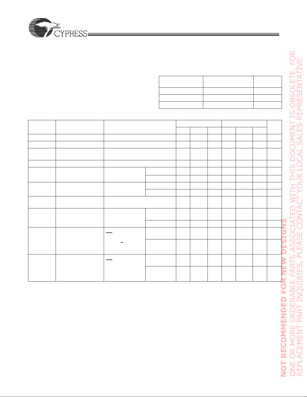
AC Test Loads and Waveforms
5V
OUTPUT
100 pF
INCLUDING
JIG AND
SCOPE
Equivalent to: THÉVENIN EQUIVALENT
OUTPUT
R1 1800
(a)
Ω
639Ω
R2
990
OUTPUT
Ω
1.77V
5V
5 pF
INCLUDING
JIG AND
SCOPE
R1 1800Ω
(b)
R2
990Ω
V
CC
GND
Rise TIme:
1 V/ns
ALL INPUT PULSES
90%
10%
90%
10%
Fall TIme
1 V/ns
Data Retention Waveform
DATA RETENTION MODE
2 V
VDR
>
CE
V
CC
1
VCC, min.
t
CDR
or
CE
2
Data Retention Characteristics
(Over the Operating Range for “LL” version only)
Parameter Description Conditions Min. Typ. Max. Unit
V
DR
I
CCDR
t
CDR
t
R
Note:
6. Tested initially and after any design or process changes that may affect t hese parameters.
VCC for Data Retention 2.0 V
Data Retention Current V
= V
CC
or CE
0.3V
= 2.0V, CE1 ≥ VCC – 0.3V,
DR
≤ 0.3V, VIN ≥ VCC – 0.3V or, VIN ≤
2
Chip Deselect to Data Retention
Time
Operation Recovery Time 70 ns
VCC, min.
t
R
1.5 15 µA
0ns
Document #: 38-05300 Rev. *C Page 4 of 11
[+] Feedback
Page 5

CY62128B
MoBL
®
Switching Characteristics
[7]
Over the Operating Range
Parameter Description
READ CYCLE
t
RC
t
AA
t
OHA
t
ACE
t
DOE
t
LZOE
t
HZOE
t
LZCE
t
HZCE
t
PU
t
PD
WRITE CYCLE
t
WC
t
SCE
t
AW
t
HA
t
SA
t
PWE
t
SD
t
HD
t
LZWE
t
HZWE
Read Cycle Time 55 70 ns
Address to Data Valid 55 70 ns
Data Hold from Address Change 5 5 ns
CE1 LOW to Data Valid, CE2 HIGH to Data Valid 55 70 ns
OE LOW to Data Valid 20 35 ns
OE LOW to Low Z 0 0 ns
OE HIGH to High Z
[7, 9]
CE1 LOW to Low Z, CE2 HIGH to Low Z
CE1 HIGH to High Z, CE2 LOW to High Z
CE1 LOW to Power-up, CE2 HIGH to Power-up 0 0 ns
CE1 HIGH to Power-down, CE2 LOW to Power-down 55 70 ns
[10]
Write Cycle Time 55 70 ns
CE1 LOW to Write End, CE2 HIGH to Write End 45 60 ns
Address Set-up to Write End 45 60 ns
Address Hold from Write End 0 0 ns
Address Set-up to Write Start 0 0 ns
WE Pulse Width 45 50 ns
Data Set-up to Write End 25 30 ns
Data Hold from Write End 0 0 ns
WE HIGH to Low Z
WE LOW to High Z
[9]
[8, 9]
[9]
[8, 9]
62128B-55 62128B-70
UnitMin. Max. Min. Max.
20 25 ns
55ns
20 25 ns
55ns
20 25 ns
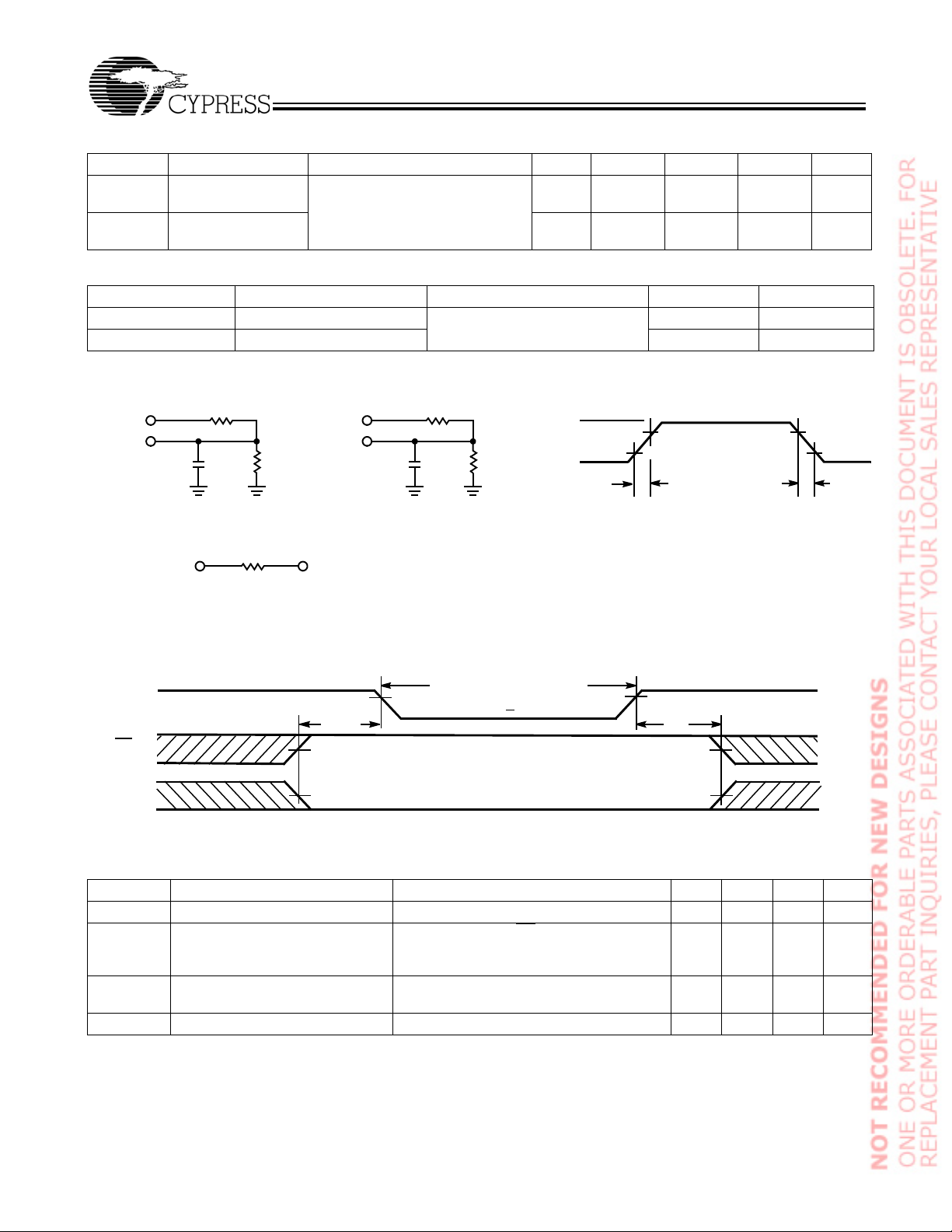
Switching Waveforms
, and t
[12, 13]
t
RC
t
t
OHA
PREVIOUS DATA VALID DATA VALID
are specified with a load capacitance of 5 pF as in (b) of AC Test Loads. Transition is measured ±500 mV fr om steady -state vo ltag e.
HZWE
CC
+ 0.5V.
, CE1 = VIL, CE2 = VIH.
HZCE
AA
is less than t
, t
LZCE
is less than t
HZOE
LOW, CE2 HIGH, and WE LOW. CE1 and WE must be LOW and CE2 HIGH to initiate a write,
1
LZOE
, and t
HZWE
is less than t
for any given device.
LZWE
Read Cycle No.1
ADDRESS
DATA OUT
Notes:
7. T est conditi ons assume signal transi tion time of 5 ns or less, t iming refer ence levels of 1.5V, input pulse le vels of 0 to 3.0V, and output loadin g of the specified
8. t
9. At any given temperature and voltage condition, t
10. The internal write time of the memory is defined by the overlap of CE
11. No input may exceed V
12. Device is continuously selected. OE
13. WE
and 100-pF load capacitan ce.
I
OL/IOH
, t
HZOE
HZCE
and the transition of any of these sign als can terminat e the write. The in put data set -up and hold timi ng should be refe renced to the leading edge of the signal that terminates
the write.
is HIGH for read cycle.
Document #: 38-05300 Rev. *C Page 5 of 11
[+] Feedback
Page 6

Switching Waveforms (continued)
PU
t
LZCE
[13, 14]
t
ACE
t
LZOE
Read Cycle No. 2 (OE Controlled)
ADDRESS
CE
1
CE
2
OE
DATA OUT
V
CC
SUPPLY
CURRENT
HIGH IMPEDANCE
t
t
DOE
50%
t
RC
t
HZOE
t
HZCE
DATA VALID
CY62128B
IMPEDANCE
t
PD
MoBL
HIGH
®
I
CC
50%
I
SB
Write Cycle No. 1 (CE1 or CE2 Controlled)
ADDRESS
CE
1
t
CE
2
WE
DATA I/O
Notes:
14. Address valid prior to or coincident with CE
15. Data I/O is high impedance if OE
16. If CE
goes HIGH or CE2 goes LOW simultaneously with WE going HIGH, the output remains in a high-impedance state.
1
= VIH.
SA
transition LOW and CE2 transition HIGH.
1
[15, 16]
t
AW
t
WC
t
SCE
t
t
PWE
t
SD
SCE
t
HA
t
HD
DATA VALID
Document #: 38-05300 Rev. *C Page 6 of 11
[+] Feedback
Page 7

Switching Waveforms (continued)
Write Cycle No. 2 (WE Controlled, OE HIGH During Write)
ADDRESS
t
SCE
CE
1
CE
2
t
SCE
t
AW
t
SA
WE
OE
[15, 16]
t
WC
t
PWE
CY62128B
MoBL
t
HA
®
DATA I/O
NOTE
17
t
HZOE
Write Cycle No.3 (WE Controlled, OE LOW)
ADDRESS
CE
1
CE
2
t
SA
WE
DATAI/O
NOTE 17
t
HZWE
[15, 16]
t
AW
t
t
SCE
SCE
t
WC
t
PWE
t
SD
DATAINVALID
t
SD
DATA VALID
t
HA
t
LZWE
t
HD
t
HD
Note:
17. During this period the I/Os are in the output state and input sig nals should not be applied.
Document #: 38-05300 Rev. *C Page 7 of 11
[+] Feedback
Page 8

Truth Table
CY62128B
MoBL
®
CE
H X X X High Z Power-down Standby (ISB)
X L X X High Z Power-down Standby (I
CE
1
LHLHData Out Read Active (I
L H X L Data In Write Active (ICC)
L H H H High Z Selected, Outputs Disabled Active (ICC)
OE WE I/O0–I/O
2
7
Mode Power
)
SB
)
CC
Ordering Information
Speed (ns) Ordering Code Package Name Package Type Operating Range
55 CY62128BLL-55SI S34 32-Lead 450-Mil SOIC Industrial
CY62128BLL-55SXI S34 32-Lead 450-Mil SOIC (Pb-Free) Industrial
CY62128BLL-55SC S34 32-Lead 450-Mil SOIC Commercial
CY62128BLL-55SXC S34 32-Lead 450-Mil SOIC (Pb-Free) Commercial
CY62128BLL-55ZI Z32 32-Lead TSOP Type I Industrial
CY62128BLL-55ZXI Z32 32-Lead TSOP Type I (Pb-Free) Industrial
CY62128BLL-55ZAI ZA32 32-Lead STSOP Type I Industrial
CY62128BLL-55ZAXI ZA32 32-Lead STSOP Type I (Pb-Free) Industrial
CY62128BLL-55ZRI ZR32 32-Lead Reverse TSOP Type I Industrial
70 CY62128BLL-70SI S34 32-Lead 450-Mil SOIC I Industrial
CY62128BLL-70SXI S34 32-Lead 450-Mil SOIC I (Pb-Free) Industrial
CY62128BLL-70SC S34 32-Lead 450-Mil SOIC I Commercial
CY62128BLL-70SXC S34 32-Lead 450-Mil SOIC I (Pb-Free) Commercial
CY62128BLL-70SE S34 32-Lead 45 0-Mil SOIC I Automotive
CY62128BLL-70SXE S34 32-Lead 450-Mil SOIC I (Pb-Free) Automotive
CY62128BLL-70ZI Z32 32-Lead TSOP Type I Industrial
CY62128BLL-70ZC Z32 32-Lead TSOP Type I Commercial
CY62128BLL-70ZE Z32 32-Lead TSOP Type I Automotive
CY62128BLL-70ZXE Z32 32-Lead TSOP Type I (Pb-Free) Automotive
CY62128BLL-70ZAI ZA32 32-Lead STSOP Type I Industrial
CY62128BLL-70ZAXI ZA32 32-Lead STSOP Type I (Pb-Free) Industrial
CY62128BLL-70ZAE ZA32 32-Lead STSOP Type I Automotive
CY62128BLL-70ZAXE ZA32 32-Lead STSOP Type I (Pb-Free) Automotive
CY62128BLL-70ZRXE ZR32 32-Lead Reverse TSOP Type I (Pb-Free) Automotive
Document #: 38-05300 Rev. *C Page 8 of 11
[+] Feedback
Page 9

Package Diagrams
17 32
32-Lead (450 MIL) Molded SOIC S34
116
0.546[13.868]
0.566[14.376]
0.440[11.176]
0.450[11.430]
CY62128B
MoBL
®
0.101[2.565]
0.111[2.819]
0.050[1.270]
BSC.
0.793[20.142]
0.817[20.751]
0.014[0.355]
0.020[0.508]
0.004[0.102]
SEATING PLANE
MIN.
0.118[2.997]
MAX.
0.004[0.102]
0.006[0.152]
0.012[0.304]
32-Lead Thin Small Outline Package Type I (8x20 mm) Z32
0.023[0.584]
0.039[0.990]
0.047[1.193]
0.063[1.600]
51-85081-*B
51-85056-*D
Document #: 38-05300 Rev. *C Page 9 of 11
[+] Feedback
Page 10

Package Diagrams (continued)
32-Lead Shrunk Thin Small Outline Package (8x13.4 mm) ZA32
CY62128B
MoBL
®
32-Lead Reverse Thin Small Outline Package ZR32
51-85094-*D
51-85089-*C
All product and company names mentioned in this document are the trademarks of their respective holders.
Document #: 38-05300 Rev. *C Page 10 of 11
© Cypress Semiconductor Corporation, 2005. The information contained herein is subject to ch an ge without notice. Cypress Semiconductor Corporation assumes no resp onsibility f or the u se
of any circuitry other than circuitry embodied in a Cypress product. Nor does it convey or imply any license under patent or other rights. Cypress products are not warranted nor intended to be
used for medical, life support, life saving, critical control or safety applications, unless pursuant to an express written agreement with Cypress. Furtherm ore, Cypress do es not authori ze its
products for use as critical components in life-support systems where a malfunction or failure may reasonably be expected to result in significant injury to the user. The inclusion of Cypress
products in life-support systems application implies that the manufacturer assumes all risk of such use and in doing so indemnifies Cypress against all charges.
[+] Feedback
Page 11

Document History Page
Document Title: CY62128B MoBL® 1-Mbit (128K x 8) St atic RAM
Document Number: 38-05300
REV. ECN NO.
** 116566 06/20/02 D SG C hanged from Spec number: 38-00524 to 38-05300
*A 126601 06/09/03 JUI Changed CE to CE
*B 23913 4 See ECN AJU Added Thermal Resistance table
*C 334398 See ECN SYT Ad ded Pb-Free part numbers to the Ordering info on Page #8
Issue
Date
Orig. of
Change Description of Change
and added CE2 ≤ 0.3V in Data Retention Characteristics table
Removed these part numbers from Ordering Information table:
CY62128BLL-55ZC, CY62128BLL-55ZAC, CY62128BLL-55ZRC,
CY62128BLL-70ZAC, CY62128BLL-70ZRI, CY62128BLL-70ZRC
Added Automotive product information
1
CY62128B
MoBL
®
Document #: 38-05300 Rev. *C Page 11 of 11
[+] Feedback
 Loading...