

128K x 8 Static RAM
fax id: 1072
CY62128
PRELIMINARY
1CY62128
Features
• 4.5V − 5.5V operation
• CMOS for optimum speed/power
• Low active power (70 ns, LL version)
—330 mW (max.) (60 mA)
• Low standby power (70 ns, LL version)
—110 µW (max.) (20 µA)
• Automatic power-down when deselected
• TTL-compatible inputs and outputs
• Easy memory expansion with CE
, CE2, and OE options
1
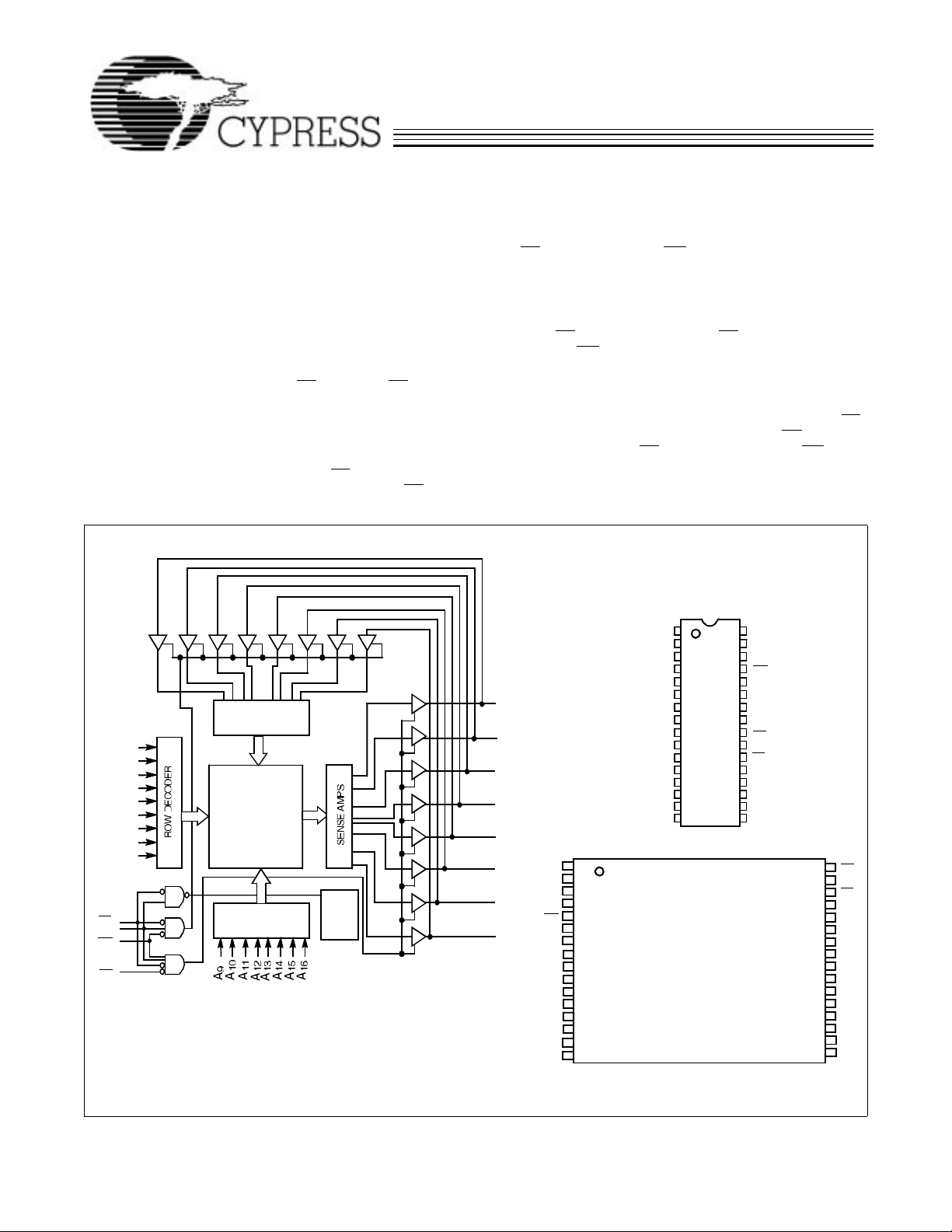
Functional Description
The CY62128 is a high-performance CMOS static RAM organized as 131,072 words by 8 bits. Easy memory expansion is
provided by an active LOW chip enable (CE
chip enable (CE
three-state drivers. This device has an automatic power-down
), an active LOW output enable (OE), a nd
2
), an active HIGH
1
Logic Block Diagram
INPUT BUFFER
A
0
A
1
A
2
A
3
A
CE
CE
WE
OE
4
A
5
A
6
A
7
A
8
1
2
512 x 256 x 8
ARRAY
COLUMN
DECODER
POWER
DOWN
feature that reduces power consumption by more than 75%
when deselected.
Writing to the device is accomplished by taking chip enable
one (CE
two (CE
I/O
pins (A
) and write enable (WE) inpu ts LOW and ch ip enable
1
) input HIGH. Data on the eight I/O pins ( I/O0 through
2
) is then written into the location specified on the address
7
through A16).
0
Reading from the device is accomplished by taking chip enable one (CE
write enable (WE
) and output enable (OE) LOW while forcing
1
) and chip enable two (CE2) HIGH. Under
these conditions, the contents of the memory location specified by the address pins will appear on the I/O pins.
The eight input/output pins (I/O
high-impedance state when the device is deselected (CE
through I/O7) are placed in a
0
HIGH or CE2 LOW), the outputs are disabled (OE HIGH), or
during a write operation (CE
LOW, CE2 HIGH, and WE LOW).
1
The CY62128 is available in a standard 400-mil-wide SOJ,
525-mil wide (450-mil-wide body width) SOIC and 32-pin
TSOP type I.
Pin
Configurations
T op View
SOJ / SOIC
V
32
CC
31
A
15
30
CE
2
29
WE
28
A
13
27
A
8
26
A
9
25
A
11
24
OE
23
A
10
22
CE
1
I/O
21
7
I/O
6
20
I/O
19
5
I/O
18
4
I/O
17
3
62128-1
I/O
I/O
I/O
I/O
I/O
I/O
I/O
I/O
NC
1
A
16
2
A
3
14
A
4
12
5
A
7
A
6
6
A
7
0
1
2
3
4
A
1
11
5
6
7
CE
V
A
WE
A
NC
A
A
A
2
A
9
3
A
8
4
13
5
6
2
7
15
8
CC
9
10
16
11
14
12
12
A
13
7
A
14
6
15
A
5
16
A
4
5
A
8
4
A
9
3
A
10
2
A
1
11
A
12
0
I/O
0
13
I/O
1
14
I/O
2
15
GND
16
TSOP I
Top View
(not to scale)
32
31
30
29
28
27
26
25
24
23
22
21
20
19
18
17
62128-2
OE
A
10
CE
I/O
I/O
I/O
I/O
I/O
GND
I/O
I/O
I/O
A
0
A
1
A
2
A
3
1
1
7
6
5
4
3
2
1
0
Cypress Semiconductor Corporation • 3901 North First Street • San Jose • CA 95134 • 408-943-2600
July 1996 - Revised November 1996
PRELIMINARY
CY62128
Selection G uide
CY62128–55 CY62128–70
Maximum Access Time (ns) 55 70
Maximum Operati ng Current Commercial 115 mA 110 mA
L 70 mA 60 mA
LL 70 mA 60 mA
Maximum CMOS Standby Current Commercial 10 mA 10 mA
L 100 µA 100 µA
LL 20 µA 20 µA
Maximum Ratings
(Above which the useful life may be impaired. For user guidelines, not tested.)
Storage Temperature .................................–65°C to +150°C
Ambient Temperature with
Power Applied.............................................–55°C to +125°C
Supply Voltage on V
DC Voltage Applied to Outputs
in High Z State
[1]
DC Input Voltage
to Relative GND
CC
..................................... –0.5V to VCC +0.5V
[1]
..................................–0.5V to VCC +0.5V
[1]
.... –0.5V to +7.0V
Electrical Characteristics Over the Operating Range
Current into Outputs (LOW) ........................................ 20 mA
Static Discharge Voltage...........................................>2001V
(per MIL-STD-883, Method 3015)
Latch-Up Current .....................................................>200 mA
Operating Range
Range
Temperature
Commercial 0°C to +70°C 5V ± 10%
[3]
Ambient
[2]
V
CC
62128–55 62128–70
Parameter Description Test Conditions Min. Max. Min. Max. Unit
V
OH
V
OL
V
IH
V
IL
I
IX
I
OZ
I
OS
I
CC
I
SB1
I
SB2
Shaded areas contain advance information
Notes:
1. V
IL
2. TA is the “instant o n” case temper ature.
3. See the last page of this specification for Group A subgroup testing information.
4. Not more than one output should be shorted at one time. Duration of the short circuit should not exceed 30 seconds.
Output HIGH Voltage VCC = Min., IOH = – 1.0 mA 2.4 2.4 V
Output LOW Voltage VCC = Min., IOL = 2.1mA 0.4 0.4 V
Input HIGH Voltage 2.2 VCC+
2.2 VCC+
0.3
Input LOW Voltage
Input Load Current GND ≤ VI ≤ V
[1]
CC
–0.3 0.8 –0.3 0.8 V
–1 +1 –1 +1 µA
Output Leakage Current GND ≤ VI ≤ VCC, Output Disabled –5 +5 –5 +5 µA
Output Short Circuit Current
VCC Operating
Supply Current
Automatic CE
Power-Down Current
—TTL Inputs
Automatic CE
Power-Down Current
— CMOS Inputs
(min.) = –2.0V fo r pu lse durations of less tha n 20 ns.
[4]
VCC = Max., V
VCC = Max.
I
= 0 mA,
OUT
f = f
MAX
= 1/t
Max. VCC, CE1 ≥ V
or CE2 < VIL,
V
≥ VIH or
IN
V
≤ VIL, f = f
IN
Max. VCC,
CE
≥ VCC – 0.3V,
1
or CE
≤ 0.3V ,
2
V
≥ VCC – 0.3V,
IN
or V
≤ 0.3V, f=0
IN
= GND –300 –300 mA
OUT
,
RC
IH
Com’l 115 110 mA
L 70 60 mA
LL 70 60 mA
Com’l 25 25 mA
L 10 10 mA
MAX
LL 2 2 mA
Com’l 10 10 mA
L 100 100 µA
LL 20 20 µA
0.3
V
2
PRELIMINARY
CY62128
Capacitance
[5]
Parameter Description Test Conditions Max. Unit
C
C
IN
OUT
Input Capacitance TA = 25°C, f = 1 MHz,
V
= 5.0V
Output Capacitance 9 pF
CC
9 pF
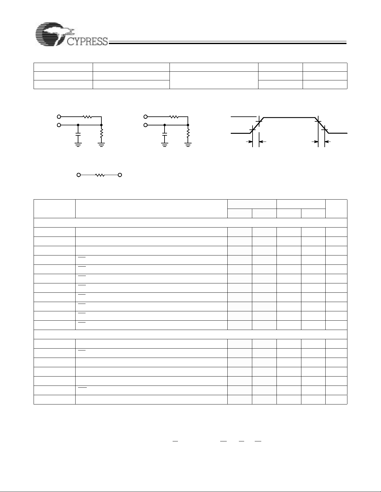
AC Test Loads and Waveforms
5V
OUTPUT
100 pF
INCLUDING
JIG AND
SCOPE
Equivalent to: THÉVENIN EQUIVALENT
OUTPUT
R1 18 00
(a)
Switching Characteristics
Ω
639Ω
OUTPUT
R2
990Ω
[3,6]
Over the Operating Range
5V
INCLUDING
JIG AND
SCOPE
1.77V
5 pF
R1 18 00 Ω
(b)
62128-3
R2
990Ω
3.0V
GND
≤ 5ns ≤ 5ns
62128–55 62128–70
Parameter Description Min. Max. Min. Max. Unit
READ CYCLE
t
RC
t
AA
t
OHA
t
ACE
t
DOE
t
LZOE
t
HZOE
t
LZCE
t
HZCE
t
PU
t
PD
WRITE CYCLE
t
WC
t
SCE
t
AW
t
HA
t
SA
t
PWE
t
SD
Shaded areas contain advance information
Notes:
5. Tested initially and after any design or process changes that may affect these parameters.
6. Test conditions assume signal transition time of 5ns or less, timing reference levels of 1.5V , input pulse levels of 0 to 3.0V, and output loading of the specified
I
and 100pF load capaci tance.
OL/IOH
7. t
8. At any given temperature and voltage condition, t
9. The internal write time of the memory is defined by the overlap of CE
, t
HZOE
and the transition of an y of th ese signal s can te rminate the write. T he inp ut dat a set- up a nd hold timi ng should be r eferenced t o th e l eading edge o f the signal that ter minates
the write.
Read Cycle Time 55 70 ns
Address to Data Valid 55 70 ns
Data Hold from Address Change 5 5 ns
CE1 LOW to Data Valid, CE2 HIGH to Data Valid 55 70 ns
OE LOW to Data Valid 20 35 ns
OE LOW to Low Z 0 0 ns
OE HIGH to High Z
CE1 LOW to Low Z, CE2 HIGH to Low Z
CE1 HIGH to High Z, CE2 LOW to High Z
[7, 8]
[8]
[7, 8]
5 5 ns
CE1 LOW to Power-Up, CE2 HIGH to Power-Up 0 0 ns
CE1 HIGH to Power-Down, CE2 LOW to Power-Down 55 70 ns
[9]
Write Cycle Time 55 70 ns
CE1 LOW to Write End, C E2 HIGH to Write End 45 60 ns
Address Set-Up to Write End 45 60 ns
Address Hold fr om Write E nd 0 0 ns
Address Set-Up to Write Start 0 0 ns
WE Pulse Width 45 50 ns
Data Set-Up to Write End 45 55 ns
HZCE
, and t
are specified with a load cap acitance of 5 pF as in part ( b) of A C Test Loads. T ran sition is meas ured ±500 mV fr om steady- state v oltag e.
HZWE
is less than t
HZCE
, t
LZCE
is less tha n t
HZOE
LOW, C E2 HIGH, and WE LOW . CE1 and WE must be LO W and CE2 HIGH to initiate a write,
1
LZOE
, and t
HZWE
is less than t
ALL INPUT PULSES
90%
10%
90%
10%
62128-4
20 25 ns
20 25 ns
for any given dev ice.
LZWE
3

PRELIMINARY
CY62128
Switching Characteristics
[3,6]
Over the Operating Range (continued)
62128–55 62128–70
Parameter Description Min. Max. Min. Max. Unit
t
HD
t
LZWE
t
HZWE
Shaded area contains advanced information.
Data Hold from Write End 0 0 ns
WE HIGH to Low Z
WE LOW to High Z
[8]
[7,8]
5 5 ns
20 25 ns
Switching Waveforms
Read Cycle No.1
ADDRESS
DATA OUT
Read Cycle No. 2 (OE Controlled)
ADDRESS
[10,11]
t
RC
t
t
OHA
AA
PREVIOUS DATA VALID DATA VALID
[11,12]
62128-5
t
RC
CE
1
CE
2
t
ACE
OE
t
DOE
t
t
LZCE
LZOE
50%
DATA OUT
V
CC
SUPPLY
HIGH IMPEDANCE
t
PU
CURRENT
Notes:
10. Device is co ntinuously selected. OE
11. WE is HIGH for read cy cle.
12. Address valid prior to or coincident with CE1 transition LOW an d CE2 transition HIG H.
, CE1 = VIL, CE2 = VIH.
DATA VALID
t
HZOE
t
HZCE
HIGH
IMPEDANCE
t
PD
ICC
50%
ISB
62128-6
4

PRELIMINARY
Switching Waveforms (continued)
Write Cycle No. 1 (CE1 or CE2 Controlled)
ADDRESS
CE
1
CE
2
WE
DATA I/O
Write Cycle No. 2 (WE Controlled, OE HIGH During Write)
[13,14]
t
SA
t
AW
t
WC
[13,14]
t
WC
t
PWE
t
SCE
t
SCE
t
SD
DATA VALID
CY62128
t
HA
t
HD
62128-7
ADDRESS
t
SCE
CE
1
CE
2
t
SCE
t
AW
t
SA
t
PWE
WE
OE
t
SD
DATA I/O
Notes:
13. Data I/O is high impedance if OE
14. If CE
15. During this period the I/Os are in the output state and input signals should not be applied.
goes HIGH or CE2 goes LOW simultaneo usly wit h WE going H IGH, t he out put remai ns in a hi gh-impedanc e state.
1
NOTE15
= VIH.
t
HZOE
DATAINVALID
t
HA
t
HD
62128-8
5

PRELIMINARY
Switching Waveforms (continued)
Write Cycle No.3 (WE Controlled, OE LOW)
ADDRESS
CE
1
CE
2
t
SA
WE
[13,14]
t
AW
t
SCE
t
SCE
t
WC
t
PWE
CY62128
t
HA
t
SD
DATAI/O
NOTE 15
t
HZWE
DATA VALID
Truth Table
CE1CE2OE WE I/O0 – I/O
7
H X X X High Z Power-Down Standby (ISB)
X L X X High Z Power-Down Standby (ISB)
L H L H Data Out Read Active (ICC)
L H X L Data In Write Active (ICC)
L H H H High Z Selected, Outputs Disabled Active (ICC)
Mode Power
Ordering Info rma tio n
Speed
(ns) Ordering Code
55 CY62128–55VC V33 3 2-Lead (400-Mil) Molded SOJ Commercial
CY62128–55SC S34 32-Lead (450-Mil) M ol ded SOIC
CY62128−55ZC Z32 32-Lead TSOP TypeI
70 CY62128–70VC V33 3 2-Lead (400-Mil) Molded SOJ Commercial
CY62128–70SC S34 32-Lead (450-Mil) M ol ded SOIC
CY62128−70ZC Z32 32-Lead TSOP Type I
CY62128L−70SC S34 32-Lead (450-Mil) M ol ded SOIC
CY62128L−70ZC Z32 32-Lead TSOP Type I
CY62128LL−70SC S34 32-Lead (4 50-Mil) Molded SOIC
CY62128LL−70ZC Z32 32-Lead TSOP Type I
Shaded area contains advanced information.
Package
Name Package Type
Operating
Range
t
LZWE
t
HD
62128-9
Document #: 38–00524
6

Package Diagrams
PRELIMINARY
32- Le ad (450 Mil) Molded SOIC S34
CY62128
32-Lead Thin Small Outline Package Z32
7

Package Diagrams (continued)
PRELIMINARY
32-Lead (400-Mil) Molded SOJ V33
CY62128
© Cypress Semiconductor Corporation, 1996. The informatio n contained herein is subject to change without notice. Cypress Semiconductor Corporation assumes no responsibility for the use
of any circ uitry other than circui try embodi ed in a Cypress Semi conductor p roduct. Nor does it convey or imply any li cense under patent or other rights . Cypress Semi conductor does not authori ze
its products for use as critical components in life-support systems where a malfunction or failure may reasonably be expected to result in significant injury to the user. The inclusion of Cypress
Semiconductor products in life-support systems application implies that the manufacturer assumes all risk of such use and in doing so indemnifies Cypress Semiconductor again st all charges.
 Loading...