

Page 1

CY4672 Reference Design Guide
Document # 001-16968 Revision **
Cypress Semiconductor
198 Champion Court
San Jose, CA 95134-1709
Phone (USA): 800.858.1810
Phone (Intnl): 408.943.2600
http://www.cypress.com
[+] Feedback
Page 2

Copyrights
Copyrights
© Cypress Semiconductor Corporation, 2007. The information contained here in is subject to ch ange wi thout noti ce. Cypress
Semiconductor Corporation assumes no responsibility for the use of any circuitry other than circuitry embodied in a Cypress
product. Nor does it convey or imply any license under patent or other rights. Cypress products are not warranted nor
intended to be used for medical, life support, life saving, critical control or sa fety applica tions, unless pursu ant to an express
written agreement with Cypress. Furthermore, Cypress does not authorize its products for use as critical components in lifesupport systems where a malfunction or failure may reasonably be expected to result in significant injury to the user. The
inclusion of Cypress products in life-support systems application implies that the manufacturer assumes all risk of such use
and in doing so indemnifies Cypress against all charges.
Cypress, the Cypress Logo, PRoC, and WirelessUSB are trademarks or registered trademarks of Cypress Semiconductor
Corporation. Windows is a registered trademark of Microsoft Corporation. All other product or company names used in this
manual may be trademarks, registered trademarks, or servicemarks of their respective owners.
Any Source Code (software and/or firmware) is owned by Cypress Semiconductor Corporation (Cypress) and is protected by
and subject to worldwide patent protection (United States and foreign), United States copyright laws and international treaty
provisions. Cypress hereby grants to licensee a personal, non-exclusive, non-transferable license to copy, use, modify, create
derivative works of, and compile the Cypress Source Code and derivative works for the sole purpose of creating custom software and or firmware in support of licensee product to be used only in conjunction with a Cypress integrated circuit as specified in the applicable agreement. Any reproduction, modification, transla tion, compilation, or representation of this Source
Code except as specified above is prohibited without the express written permission of Cypress.
Disclaimer
CYPRESS MAKES NO WARRANTY OF ANY KIND, EXPRESS OR IMPLIED, WITH REGARD TO THIS MATERIAL,
INCLUDING, BUT NOT LIMITED TO, THE IMPLIED WARRANTIES OF MERCHANTABILITY AND FITNESS FOR A PARTICULAR PURPOSE. Cypress reserves the right to make changes without furthe r notice to the materials described herein.
Cypress does not assume any liability arising out of the application or use of any product or circuit described herein. Cypress
does not authorize its products for use as critical components in life-support systems where a malfunction or failure may reasonably be expected to result in significant injury to the user . The inclusion of Cypress ' product in a life-support systems application implies that the manufacturer assumes all risk of such use and in doing so indemnifies Cypress against all charges.
Use may be limited by and subject to the applicable Cypress software license agreement.
2 CY4672 Reference Design Guide, Document # 001-16968 Revision **
[+] Feedback
Page 3

Contents
1. Introduction 9
1.1 Scope...........................................................................................................................9
1.2 Chapter Overviews ...................................... ... ... ... ... .... ...................................... .... ... ..9
1.3 Support........................................................................................................................9
1.4 Conventions...............................................................................................................10
2. WirelessUSB™ Protocol 2.2 13
2.1 General Overview...................................................................... ... ... ... ... ....................13
2.2 Protocol Modes..........................................................................................................15
2.3 Packet Structures ......................................................................................................23
2.4 Bind and Reconnect Timing............. ... ... ....................................... ... ... ... .... ... ... ... .... ...26
2.5 Signature Byte ...........................................................................................................28
2.6 Encryption ............................. ....................................................... .............................29
1.4.1 Definitions ......................................................................................................10
1.4.2 Acronyms.......................................................................................................10
2.1.1 Radio Channel Management .........................................................................13
2.1.2 Pseudo Noise Codes .....................................................................................13
2.1.3 Chip Error Correction........................................................ ... ... .......................14
2.1.4 Automatic Acknowledgment (AutoACK).........................................................14
2.1.5 Network ID .....................................................................................................14
2.1.6 Manufacturing ID........................ ... .... ... ... ... ....................................... ... ... .... ...14
2.1.7 Channel Selection Algorithm................................... ... .... ... ... ... ... .... ... ... ... .... ...15
2.2.1 Ping Mode (Bridge Only)................................... ... ..........................................16
2.2.2 Idle Mode (HID only).................................................. .... ... ... ... ... ....................17
2.2.3 Reconnect Mode (HID only)...........................................................................17
2.2.4 Button Bind Mode.......................... .... ...................................... ... .... ... ... ... .... ...17
2.2.5 Enhanced KISSBind™...................................................................................18
2.2.6 Unbind............................................................................................................20
2.2.7 Data Mode........................ .... ... ... ... ....................................... ... ... .... ... ... ... .... ...20
2.2.8 Back Channel Data Support...........................................................................20
2.2.9 Dynamic Data Rate and Dynamic PA.............................................................22
2.3.1 Bind/KISSBind Request Packet (HID) ...........................................................23
2.3.2 Bind Response Packet (Bridge) ... .... ... ... ... ... .... ... ... ... .... ... ... ... ... .... ... ... ... .... ...24
2.3.3 Connect Request (HID)........................... ... ... .... ... ... ... .... ... ... ..........................24
2.3.4 Connect Response Packet (Bridge)...............................................................24
2.3.5 Ping Packet (Bridge) .............................................. ... .... ... ............................. 25
2.3.6 Data Packet/Back Channel Data Packet (Bridge and HID)............................25
2.6.1 TEA Encryption..............................................................................................29
2.6.1.1 TEA Key Management over WirelessUSB.......................................29
2.6.2 AES Encryption..............................................................................................30
2.6.2.1 AES Key Management.....................................................................31
2.6.3 Encryption and Power Consumption Trade Off..............................................31
CY4672 Reference Design Guide, Document # 001-16968 Revision ** 3
[+] Feedback
Page 4

Contents
3. Mouse 33
3.1 Introduction................................................................................................................33
3.1.1 Design Features ..................................... .... ... ... ... ... .... ... ... .............................33
3.2 Hardware Overview...................................................................................................33
3.2.1 RDK Mouse Assembly...................................................................................33
3.2.2 Hardware Block Diagram...............................................................................35
3.2.3 Schematics ...................................................................................................35
3.2.4 Hardware Considerations .............................................................................36
3.3 Firmware Architecture ...............................................................................................36
3.3.1 ROM/RAM Usage..........................................................................................36
3.3.2 PRoC LP Device Configuration......................................................................36
3.3.2.1 Global Configuration................. .... ... ... ... ... .... ... ... ... .... ... ... ... .............38
3.3.2.2 SPI Master User Module .................................................................38
3.3.2.3 Programmable Interval Timer User Module.....................................39
3.3.2.4 Flash Security........... ... .... ... ... ....................................... ... ... ... .... ......39
3.3.3 Model.............................................................................................................39
3.3.4 Common Code...............................................................................................40
3.3.4.1 Generated Library Code..................................................................40
3.3.4.2 Debounce Module ...........................................................................40
3.3.4.3 SPI Module............................ ... .... ... ...................................... .... ... ...40
3.3.4.4 Radio Driver.....................................................................................41
3.3.4.5 Protocol Module...............................................................................41
3.3.4.6 Flash Module...................... ... ... .... ... ... ... ....................................... ...41
3.3.4.7 Port Module ........................................................................ ... .... ... ...41
3.3.4.8 Poll Module......................................................................................41
3.3.4.9 Timer Module...................................................................................41
3.3.4.10 ISR Module......................................................................................42
3.3.5 Application Code............................................................................................42
3.3.5.1 Mouse Module.................................................................................42
3.3.5.2 Optical Module.... ... ... ... .... ... ... ... .... ...................................... ... .... ... ...43
3.3.5.3 Testmode Module............................................................................43
3.3.5.4 Buttons Module................................................................................44
3.3.5.5 Mfgtest Module................................................................................44
3.3.5.6 Wheel Module..................................................................................44
3.3.5.7 Battery Module ................................................................................45
3.3.6 Configuration Options....................................................................................45
3.3.6.1 MOUSE_REPORT_IN_MS .............................................................45
3.3.6.2 MOUSE_ACTIVE_MS.....................................................................45
3.3.6.3 MOUSE_DISCONNECTED_POLL_MS..........................................45
3.3.6.4 MOUSE_TX_TIMEOUT_MS ...........................................................45
3.3.6.5 MOUSE_CONNECT_ATTEMPT_TIMES........................................46
3.3.6.6 PLATFORM_H ................................................................................46
3.3.6.7 MOUSE_800_NOT_400_CPI..........................................................46
3.3.6.8 MOUSE_BATTERY_STATUS.........................................................46
3.3.6.9 MOUSE_TEST_MODE ...................................................................46
3.3.6.10 MFG_TEST_CODE.........................................................................46
3.3.6.11 MFG_TX_MODES...........................................................................46
3.3.6.12 MASTER_PROTOCOL ...................................................................46
3.3.6.13 PAYLOAD_LENGTH.......................................................................46
3.3.6.14 KISS_BIND......................................................................................47
3.3.6.15 RSSI_QUALIFY...............................................................................47
3.3.6.16 AUTO_CONNECT...........................................................................47
3.3.7 Platform and Architecture Portability..............................................................47
4 CY4672 Reference Design Guide, Document # 001-16968 Revision **
[+] Feedback
Page 5

Contents
3.3.8 Initialization ....................................................................................................47
3.3.9 Wireless Protocol Data Payload.....................................................................47
3.3.9.1 Packet Format 1...............................................................................48
3.3.9.2 Packet Format 2...............................................................................48
3.3.9.3 Packet Format 3...............................................................................48
3.3.10 Interrupt usage and timing ............ .... ... ... ... ... .... ...................................... .... ...48
3.3.11 Code Performance Analysis...........................................................................49
3.4 Development Environment .... ... ... .... .......................................... ... ............................. 49
3.4.1 Tools...............................................................................................................49
3.4.2 Tips and Tricks ...............................................................................................50
3.4.2.1 M8C Sleep.......................................................................................50
3.4.2.2 Watchdog Timer...............................................................................50
3.4.3 Critical Test Points..........................................................................................50
4. Keyboard 51
4.1 Introduction................................................................................................................51
4.1.1 Design Features................................ ... ... ... ... .... ... ... ... .... ................................51
4.2 Hardware Overview ...................................................................................................51
4.2.1 RDK Keyboard Assembly...............................................................................52
4.2.2 Schematic ......................................................................................................54
4.2.3 Keyboard Matrix.............................................................................................55
4.2.4 Hardware Considerations...............................................................................55
4.3 Firmware Architecture................................................................................................56
4.3.1 ROM/RAM usage...........................................................................................56
4.3.2 enCoRe II Device Configuration.....................................................................56
4.3.2.1 Global Configuration.............. ... ... ... .... ... ... ... .... ... ... ... ... .... ... ... ... .......58
4.3.2.2 SPI Master User Module..................................................................59
4.3.2.3 Programmable Interval Timer User Module.....................................59
4.3.2.4 Flash Security........ ... ... ... .... ... ... ... ... ....................................... ... .... ...59
4.3.3 Model .............................................................................................................60
4.3.4 Common Code...............................................................................................60
4.3.4.1 Generated Library Code ..................................................................60
4.3.4.2 Radio Driver.....................................................................................60
4.3.4.3 Protocol Module...............................................................................61
4.3.4.4 Flash Module .................. .... ... ... ... ... .... ... ... ... .... ................................61
4.3.4.5 ISR Module......................................................................................61
4.3.4.6 Timer Module...................................................................................61
4.3.5 Application Code............................................................................................61
4.3.5.1 Keyboard Module.............................................................................61
4.3.5.2 Mfgtest Module ................................................................................62
4.3.5.3 Battery Module.................................................................................62
4.3.5.4 Test Module.....................................................................................62
4.3.5.5 Encrypt Module................................................................................63
4.3.6 Configuration Options ....................................................................................63
4.3.6.1 KEYBOARD_KEEP_ALIVE_TIMEOUT...........................................63
4.3.6.2 KEY_DOWN_DELAY_SAMPLE_PERIOD......................................63
4.3.6.3 KEYBOARD_DEBOUNCE_COUNT................................................63
4.3.6.4 KEYBOARD_MULTIMEDIA_SUPPORT .........................................63
4.3.6.5 KEYBOARD_TEST_MODES...........................................................64
4.3.6.6 KEYBOARD_TEST_MODE_PERIOD.............................................64
4.3.6.7 PANGRAM_TEST_MODE...............................................................64
4.3.6.8 KEYBOARD_BATTERY_VOLTAGE_SUPPORT............................64
4.3.6.9 LP_RDK_KEYBOARD_MATRIX .....................................................64
CY4672 Reference Design Guide, Document # 001-16968 Revision ** 5
[+] Feedback
Page 6

Contents
4.3.6.10 KEYBOARD_TX_TIMEOUT............................................................64
4.3.6.11 TIMER_CAL ....................................................................................64
4.3.6.12 ENCRYPT_TEA ..............................................................................64
4.3.6.13 ENCRYPT_AES ..............................................................................64
4.3.6.14 MFG_TEST_CODE.........................................................................64
4.3.6.15 MFG_ENTER_BY_PIN....................................................................64
4.3.6.16 MFG_TX_MODES...........................................................................65
4.3.6.17 MOUSE_EMULATION_MODE........................................................65
4.3.6.18 BACK_CHANNEL_SUPPORT ........................................................65
4.3.6.19 MASTER_PROTOCOL ...................................................................65
4.3.6.20 PAYLOAD_LENGTH.......................................................................65
4.3.6.21 KISS_BIND......................................................................................65
4.3.6.22 RSSI_QUALIFY...............................................................................65
4.3.6.23 PLATFORM_H ................................................................................65
4.3.7 Platform and Architecture Portability..............................................................65
4.3.8 Initialization....................................................................................................66
4.3.9 Wireless Protocol Data Payload ....................................................................66
4.3.9.1 Keyboard Application Report Formats.............................................66
4.3.10 Ghost Key Detection............ ... ... .... ...................................... .... ... ... ... ... .... ... ...70
4.3.11 Interrupt Usage / Timing ................................................................................70
4.3.12 Code Performance Analysis ..........................................................................71
4.4 Modifying the Keyboard Matrix or Adding New Keys ................................................72
4.4.1 Modifying the Keyboard Matrix ......................................................................72
4.4.2 Adding New Keys ....................................... ... ... ... ... .... ... ... ... ..........................72
4.5 Development Environment....... .... ... ... ....................................... ... ... .... ... ... ... ... .... ... ...73
4.5.1 Tools ..............................................................................................................73
4.5.2 Tips and Tricks...............................................................................................73
4.5.2.1 M8C Sleep.......................................................................................73
4.5.2.2 Watchdog Timer ..............................................................................73
4.5.3 Critical Test Points .........................................................................................74
5. Bridge 75
5.1 Introduction................................................................................................................75
5.1.1 Design Features ..................................... .... ... ... ... ... .... ... ... .............................75
5.2 Hardware Overview...................................................................................................75
5.2.1 Bridge Photographs....................... ... ... ... .... ...................................... ... .... ... ...76
5.2.2 In-System Programming................................................................................76
5.2.3 Schematics ....................................................................................................77
5.2.4 LED Usage ....................................................................................................77
5.3 Firmware Architecture ...............................................................................................78
5.3.1 ROM/RAM Usage..........................................................................................78
5.3.2 PRoC LP Device Configuration......................................................................78
5.3.2.1 Global Configuration................. .... ... ... ... ... .... ... ... ... .... ... ... ... .............80
5.3.2.2 SPI Master User Module .................................................................81
5.3.2.3 USB Device User Module................................................................81
5.3.2.4 1 Millisecond Interval Timer User Module .......................................81
5.3.2.5 Flash Security........... ... .... ... ... ....................................... ... ... ... .... ......81
5.3.3 Model.............................................................................................................82
5.3.4 Common Code...............................................................................................82
5.3.4.1 PSoC Generated Library Code........................................................82
5.3.4.2 Flash................................................................................................83
5.3.4.3 Timer ...............................................................................................83
5.3.4.4 Radio Driver.....................................................................................83
6 CY4672 Reference Design Guide, Document # 001-16968 Revision **
[+] Feedback
Page 7

Contents
5.3.4.5 Master Protocol................................................................................83
5.3.5 Application Code............................................................................................83
5.3.5.1 Bridge Module . ... .... ... ... ... .... ... ... ....................................... ... ... ... .... ...83
5.3.5.2 USB Module . ... ... .... ... ... ... .... ... ... ... ... ....................................... ... .... ...84
5.3.5.3 Mfgtest Module ................................................................................84
5.3.5.4 Encrypt Module................................................................................84
5.3.6 Configuration Options ....................................................................................85
5.3.6.1 MFG_TEST_CODE .........................................................................85
5.3.6.2 MFG_TX_MODES...........................................................................85
5.3.6.3 MFG_ENTER_BY_PIN....................................................................85
5.3.6.4 MFG_ENTER_BY_BUTTON...........................................................85
5.3.6.5 MFG_ENTER_BY_USBSE1............................................................85
5.3.6.6 ENCRYPT_TEA...............................................................................85
5.3.6.7 ENCRYPT_AES...............................................................................85
5.3.6.8 GREEN_LED_ON_TIME.................................................................85
5.3.6.9 DOWNKEY_TIME_OUT..................................................................85
5.3.6.10 BACK_CHANNEL_SUPPORT.........................................................86
5.3.6.11 MASTER_PROTOCOL....................................................................86
5.3.6.12 PAYLOAD_LENGTH .......................................................................86
5.3.6.13 POWER_BIND.................................................................................86
5.3.6.14 KISS_BIND......................................................................................86
5.3.6.15 RSSI_QUALIFY...............................................................................86
5.3.6.16 PROMISCUOUS_MODE.................................................................86
5.3.6.17 DAL_ENABLE..................................................................................86
5.3.7 Platform and Architecture Portability..............................................................87
5.3.8 Initialization ....................................................................................................87
5.3.9 Wireless Protocol Data Payload.....................................................................87
5.3.10 Suspend and Remote Wakeup......................................................................87
5.3.11 Interrupt Usage/Timing.................. .... ... ... ... ... .... ... ... ... .... ................................87
5.3.12 Code Performance Analysis...........................................................................88
5.4 USB Interface ........ ... ... ... .... ... ....................................... ... ... ... .... ... ... ... .......................88
5.4.1 USB Descriptors...................... ... ... .... ... ... ... ... .... ... ....................................... ...88
5.4.1.1 Device/Config Descriptors ...............................................................89
5.4.1.2 Keyboard HID Report Descriptor.....................................................89
5.4.1.3 Mouse/Keyboard HID Report Descriptor .........................................90
5.4.2 Keyboard Report Format................................................................................93
5.4.3 Mouse Report Format....................................................................................95
5.4.4 Battery Level and Link Quality Reports..........................................................95
5.4.4.1 Requesting a New Battery Reading .... ... ... ... .... ... ... ... ... .... ... ... ... .... ...96
5.4.4.2 Obtaining the RadioParams Report.................................................96
5.4.5 Example USB Bus Analyzer (CATC) Traces..................................................97
5.5 Development and Debug Environment....................................................................100
5.5.1 Tools.............................................................................................................100
5.5.2 Tips and Tricks .............................................................................................100
6. Manufacturing Test Support, MTK 101
6.1 Introduction..............................................................................................................101
6.2 MTK Block Diagram.................................................................................................101
6.3 MTK Serial Protocol.................................................................................................101
6.4 MTK RF Protocol .....................................................................................................103
6.5 MTK DUT Source Code Porting ..............................................................................103
6.6 Accessing MTK in the DUT .....................................................................................103
CY4672 Reference Design Guide, Document # 001-16968 Revision ** 7
[+] Feedback
Page 8

Contents
7. Regulatory Testing Results 105
7.1 Introduction..............................................................................................................105
8. Power Considerations 107
8.1 RDK Keyboard.........................................................................................................107
8.1.1 Usage Model..... ... ... ... ... .... ...................................... .... ... ... ... ........................107
8.1.2 Current Measurements..................... ... ... .... ... ... ... ... .... ... ... ... .... ... ... ... ...........107
8.1.3 Battery Life Calculations..............................................................................108
8.2 RDK Mouse.............................................................................................................108
8.2.1 Usage Model..... ... ... ... ... .... ...................................... .... ... ... ... ........................108
8.2.2 Current Measurements..................... ... ... .... ... ... ... ... .... ... ... ... .... ... ... ... ...........109
8.2.3 Battery Life Calculations..............................................................................109
9. Software Guide 111
9.1 Introduction..............................................................................................................111
9.2 Software Code Modules............... ... ... ... ....................................... ... .... ... ... ... ... .... ... .111
9.2.1 USB HID API module. ... .... ... ... ... .... ... ... ....................................... ... ... ... .... ... . 111
9.2.1.1 CHidDevice Class Methods...........................................................112
9.2.1.2 CHidManager Class Methods........................................................113
9.2.2 System Tray Module.. ... ....................................... ... .... ................................. 114
9.2.2.1 CCySysTray Class Methods..........................................................114
9.2.3 WirelessUSB System Tray Application Module........................................... 115
9.2.3.1 CWirelessUSBTrayApp Class Methods ........................................115
9.2.3.2 CMainFrame Class Methods.........................................................116
9.2.3.3 CWirelessUSBStatusPropertyPage Class Methods......................117
9.2.3.4 CWirelessUSBStatusPropertySheet Class Methods.....................117
9.2.3.5 CHidTrayDevice Class Methods....................................................118
9.2.3.6 CHidTrayManager Class Methods ................................................118
9.3 Development Environment....... .... ... ....................................... ... ... ... .... ... ... ... ... .... ... .118
Appendix A. References 119
Index 121
Revision History 125
8 CY4672 Reference Design Guide, Document # 001-16968 Revision **
[+] Feedback
Page 9

1. Introduction
1.1 Scope
This document was written for firmware an d hard ware develop ers th at want to und erst a nd an d make
modifications to the PRoC™ LP KBM Reference Design Kit (RDK).
This document provides a description of the hardware along with architecture and configuration
options for the PRoC LP KBM RDK.
1.2 Chapter Overviews
Table 1-1. Overview of the CY4672 Reference Design Guide Chapters
Chapter Description
Introduction
(on page 9)
WirelessUSB™ Protocol 2.2
(on page 13)
Mouse
(on page 33)
Keyboard
(on page 51)
Bridge
(on page 75)
Manufacturing Test Support, MTK
(on page 101)
Regulatory Testing Results
(on page 105)
Power Considerations
(on page 107)
Software Guide
(on page 111)
Describes the purpose of this guide, overviews each chapter, supplies
product support information, and lists documentation conventions.
Presents an overview of the radio channel management and pseudo
noise code. Lists the protocol modes, packet structures, bind and reconnect timing, signature byte and the encryption methods.
Discusses the design features, hardware, firmware architecture, and the
development environment.
Describes the design features, hardware, firmware architecture, modifying the keyboard matrix or adding new keys, and the development environment.
Describes the design features, hardware, firmware architecture, USB
interface, and the development and debut environment.
Details the MTK block diagram, MTK serial protocol, MTK RF protocol,
MTK DUT source code porting, and accessing MTK in the DUT.
Describes all EMC test results.
Details the usage mode, current measurments, and battery life calcula-
tions for both the RDK keyboard and RDK mouse.
Describes software code modules and the development environment.
1.3 Support
Technical Support can be reached at http://www.cypress.com/support or can be contacted by phone
at: 1-800-541-4736.
CY4672 Reference Design Guide, Document # 001-16968 Revision ** 9
[+] Feedback
Page 10

Introduction
1.4 Conventions
The following are easily identifiable conventions used throughout this user guide.
Table 1-2. Documentation Conventions
Convention Usage
Courier New
Size 12
Italics Displays file names and reference documentation:
[bracketed, bold] Displays keyboard commands in procedures:
File > New Project Represents menu paths:
Bold Displays commands, menu paths and selections, and icon
1.4.1 Definitions
The following are some definitions of words found in this document. There may be other meanings to
these definitions outside of this document.
Displays file locations and source code:
C:\ …cd\icc\, user entered text.
sourcefile.hex
[Enter] or [Ctrl] [C]
File > New Project > Clone
names in procedures:
Click the Debugger icon, and then click Next.
Bridge – The bridge is the receiving radio and USB hardware that connects to the PC and enumerates as a Human Interface Device.
Device – The reference to device in this document means the keyboard or mouse device that is
sending radio packets to the bridge.
1.4.2 Acronyms
The following are acronyms used throughout this user guide.
Table 1-3. Acronyms
Acronym Description
AES advanced encryption standard
ADC analog-to-digital converter
API application programming interface
CRC cyclic redundancy check; mechanism to help detect errors
DSSS direct sequence spread spectrum communication
DVK
HID
MID manufacturing ID
PN codes
development kit. It is produced by Cypress Semiconductor for
showcasing Cypress products with a working development
environment
human interface device. It is a product that allows an individual to interface with a computer. A keyboard and mouse are
HID devices
pseudo noise codes; WirelessUSB™ systems encode their
data within PN codes
10 CY4672 Reference Design Guide, Document # 001-16968 Revision **
[+] Feedback
Page 11

Table 1-3. Acronyms (continued)
Acronym Description
reference design kit; it is produced by Cypress Semiconductor
and used by third parties to produce off-the-shelf products.
RDK
RSSI receive signal strength indicator
SOP start of packet
TEA tiny encryption algorithm
USB
WirelessUSB a trademark name for Cypress 2.4 GHz radio products
Everything required to take a product to production is included
in the kit. This document is part of the CY4672 Keyboard/
Mouse RDK
universal serial bus; a well-known serial standard used in the
computing world
Introduction
CY4672 Reference Design Guide, Document # 001-16968 Revision ** 11
[+] Feedback
Page 12

Introduction
12 CY4672 Reference Design Guide, Document # 001-16968 Revision **
[+] Feedback
Page 13
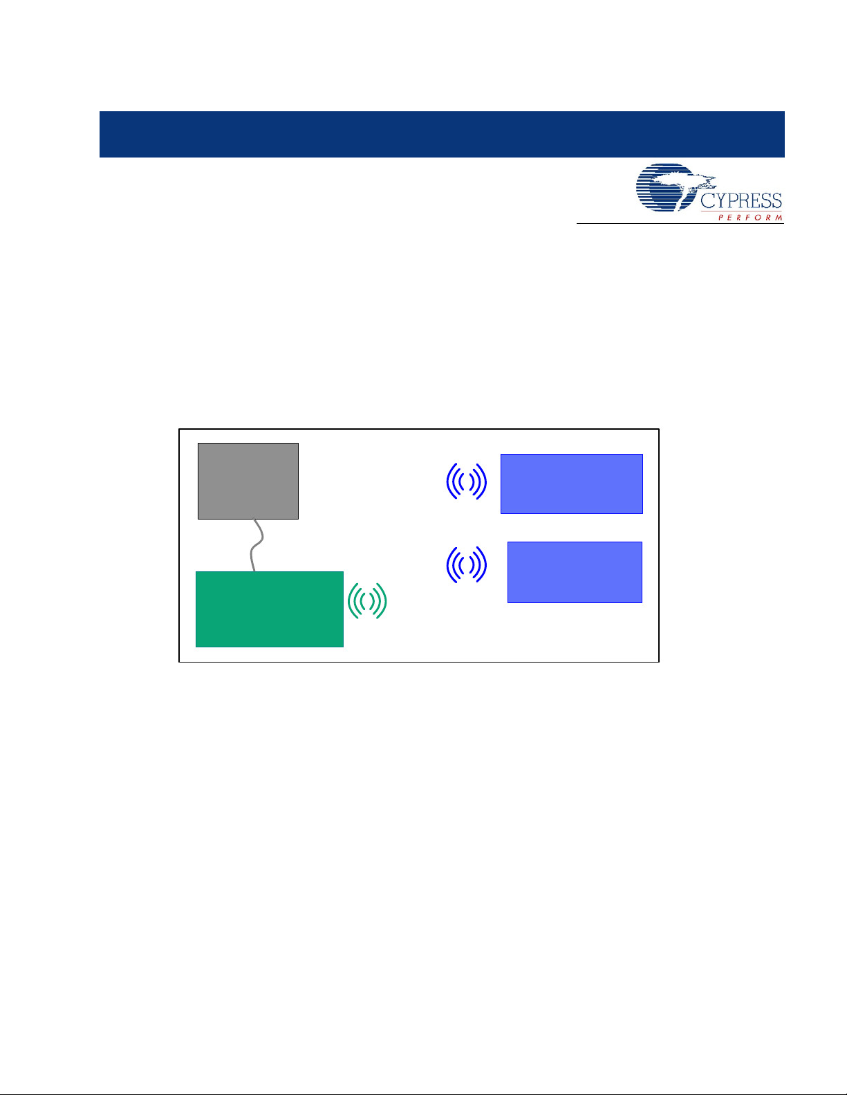
2. WirelessUSB™ Protocol 2.2
Host PC
or Laptop
WirelessUSB
Keyboard
(Transceiver)
WirelessUSB
Mouse
(Transceiver)
WirelessUSB-LS
Bridge
(Transceiver)
USB
-
2.1 General Overview
The WirelessUSB™ protocol 2.2 is designed to address 2-way Human Interface Devices (HID) as
well as general purpose devices; it provides reliable 2-way communication between a wireless
device configured as 1:1 (one HID and one bridge) or 2:1 (two HIDs and one bridge) systems. The
WirelessUSB protocol 2.2 allows HID applications to establish a connection to the bridge and
receive ACK and DATA packets from the bridge.
Figure 2-1. WirelessUSB 2-Way System
2.1.1 Radio Channel Management
2.1.2 Pseudo Noise Codes
CY4672 Reference Design Guide, Document # 001-16968 Revision ** 13
WirelessUSB uses the unlicensed 2.4 GHz Industrial, Scientific, and Medical (ISM) band for wireless
connectivity. WirelessUSB uses 78 of the available channels and splits the 78 channels into 6 channel subsets consisting of 13 channels ea ch. T h e channel subsets are used by each n et wor k t o m in i mize the probability of interference from other WirelessUSB systems (see the Channel Selection
Algorithm on page 15 section for more details). A designated channel subset is used during bind
mode (along with an associated pseudo noise code) in order to enable all WirelessUSB devices to
effectively communicate during this procedure.
Pseudo noise codes (PN codes) are the codes used to achieve the special matched filter characteristics of direct sequence spread spectrum (DSSS) communication. Certain codes referred to as ‘multiplicative codes’ are used for WirelessUSB 2-way communication. These codes have minim al crosscorrelation properties, meaning they are less susceptible to interference caused by overlapping
transmissions on the same channel. The length of the PN code results in different communication
characteristics. Higher data rates are achieved with 32-chips/bit PN codes, while 64-chips/bit PN
codes allow a longer range. The number of frequency/code pairs is large enough to comfortably
[+] Feedback
Page 14

WirelessUSB™ Protocol 2.2
accommodate hundreds of WirelessUSB devices in the same space. Each bridge/HID pair must use
the same PN code and channel in order to communicate with each other.
2.1.3 Chip Error Correction
In the presence of interference (or near the limits of range), the transmitted PN code will often be
received with some PN code chips corrupted. DSSS receivers use a data correlator to decode the
incoming data stream. WirelessUSB LP supports a separate start of packet (SOP) and data threshold. The RDK uses an SOP threshold of ‘4’. The data threshold is set to the default value of ‘4’.
2.1.4 Automatic Acknowledgment (AutoACK)
The WirelessUSB LP radio contains an autom atic acknowledgment feature that allows it to automatically send an ACK to any valid packet that is received. The WirelessUSB LP radio also uses the
concept of transactions to allow the radio in the HID to automatically power down after transmitting a
packet and receiving an AutoACK instead of waiting for the firmware to power the radio down. This
conserves power and reduces the firmware complexity of WirelessUSB applications.
2.1.5 Network ID
The network ID contains the parameters for the channel selection algorithm as well as the PN code
to be used. HIDs retrieve the network ID information from the bridge during the bind procedure. A
special network ID is reserved for bind mod e, known as the bind ID. The bind ID gives a common
channel subset so that any two devices can communicate with each other during bind mode. The
network ID is composed of the following fields:
PIN This is a random number between 2–5 that defines the channel subset and is
used in the channel selection algorithm.
Base Channel This is the first channel to be used in the channel selection algorithm, that deter-
mines which channels are contained in the channel subset.
PN Code This is used as an index to select one of 10 used SOP PN codes, as noted in the
radio driver document.
CRC Seed This 8-bit value is used for the CRC calculation, that further diversifies transmis-
sions from different networks. All packets sent between non-bound devices use
the default CRC seed of 0x0000. All packets sent between bound devices use a
CRC seed that is common to all devices bound to a particular bridge or network
but unique from network to network.
2.1.6 Manufacturing ID
Each WirelessUSB radio contains a 4-byte manufacturing ID (MID), that has been laser fused into
the device during manufacturing. The bridge uses its MID to help randomize channel subsets, PN
codes and network CRC seeds. The bridge sends its MID to the HIDs when binding. The HID then
stores the bridge’s MID in non-volatile memory after binding. The HID sends the bridge’ s MID as p art
of the connect request packet, allowing the bridge to verify the identity of the HID when establishing
a connection.
Both the bridge and the HID use the bridge’ s MID as to generate the device network ID compon ent s.
The following equations ensure that each network will have a unique set of network ID components:
PN Code = [(mid_1 << 2) + mid_2 + mid_3] mod 10
Base Channel = [(mid_2 >> 2) – (mid_1 << 5) + mid_3] mod 78
PIN = [(((mid_1 -mid_2) & PIN_MASK) + MIN_PIN)] mod 78
CRC Seed = ((mid_2 >> 6)) + mid_1 + mid_3 if=0 then Seed = 1
14 CY4672 Reference Design Guide, Document # 001-16968 Revision **
[+] Feedback
Page 15
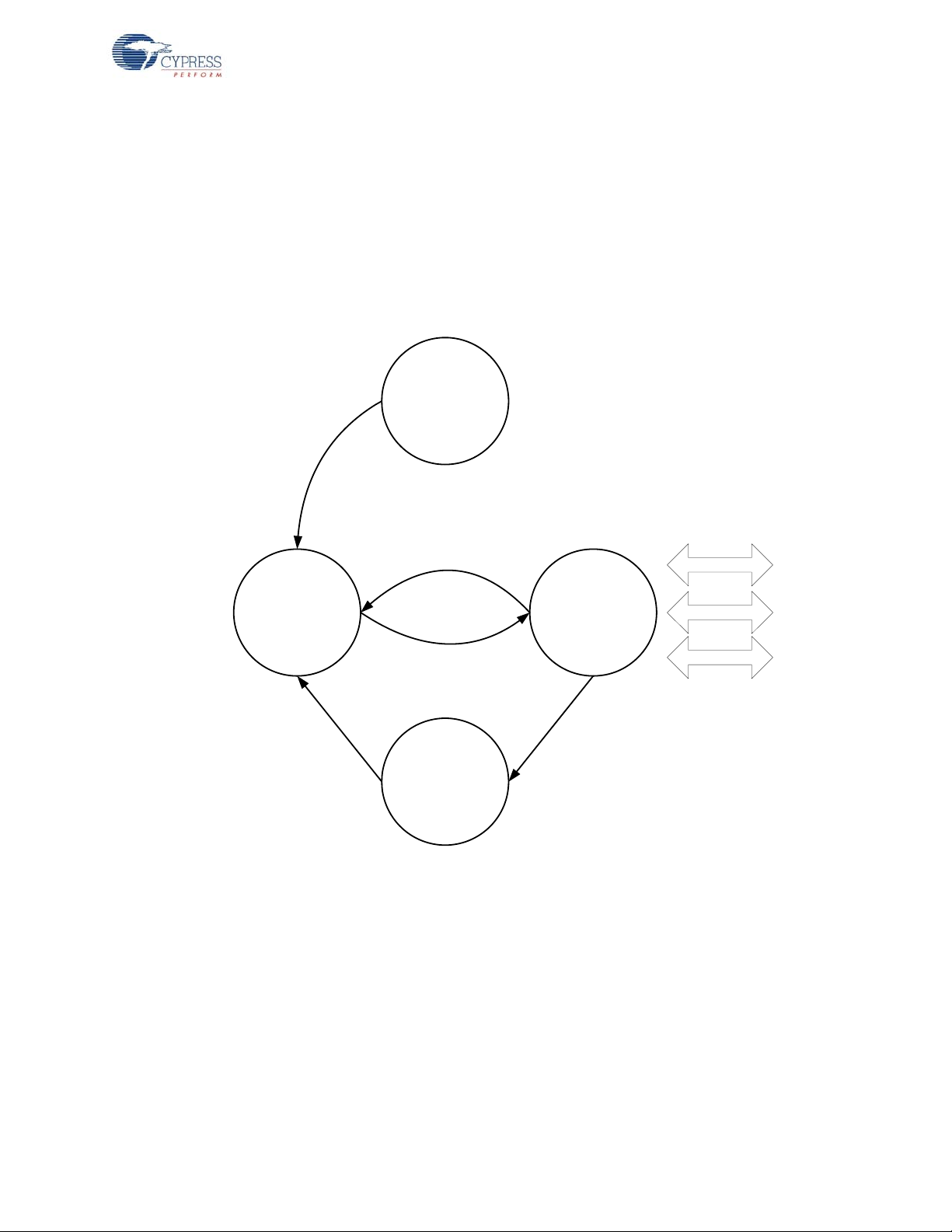
2.1.7 Channel Selection Algorithm
POR
Ping
Mode
Data
Mode
Manual
Bind Mode
Connected Data
KISSBind
Ping
Ping for other networks,
sample the background
RSSI
Bind channel
and PN code
Connected channel and
PN Code
Background RSSI or Link
quality exceeded
The channel selection algorithm produces a subset containing 13 of the possible 78 channels. The
channel selection algorithm is based on the network ID, with each channel in the subset being six
megahertz from the nearest neighboring channels in the subset. This algor ithm r educes the possibility of multiple bridges selecting the same channels in the same order at the same time.
2.2 Protocol Modes
Figure 2-2. Protocol Master
WirelessUSB™ Protocol 2.2
CY4672 Reference Design Guide, Document # 001-16968 Revision ** 15
[+] Feedback
Page 16
WirelessUSB™ Protocol 2.2
POR
Idle
Mode
Bind
Mode
Data
Mode
Reconnect
Mode
Bound
UnBound,
KISSBind disabled
Wait for
user Bind
event
KISSBind
Mode
UnBound,
KISSBind enabled
Bind fails
Lost
connection
with bridge
Bridge
found
Search for bridge
and sleep if
necessary
Sleep when no data
to be sent
Figure 2-3. Protocol Slave
2.2.1 Ping Mode (Bridge Only)
Ping mode is used by the bridge to find an available channel; channels are unavailable if they are
being used by another network with the same PN code, or if there is excessive noise on the chann el.
The bridge first listens for activity on the selected chan nel. If the chan nel is inactive the bridge alter nately transmits ping packets and listens for ping response packets for a defined* period of time.
During ping mode the bridge also checks the Receive Signal Strength Indicator (RSSI) of the radio in
order to determine if a non-WirelessUSB device is using this channel (or a WirelessUSB device on
the same channel using a different PN code). If a ping response is received, indicating that another
bridge is using this channel the bridge selects the next channel using the ch annel selection algor ithm
and repeats this procedure. The bridge also selects another channel using the channel selection
algorithm if RSSI is high; this indicates that there are other RF sources on the ch annel. If a ping
response is not received and RSSI is low, the bridge assumes the ch annel is available a nd moves to
data mode. Bridges send ping response packets in response to all received ping packets if the
bridge is in data mode. HIDs never respond to ping packets.
[*The timeout value is configurable using the PING_NUM_RSSI define.]
16 CY4672 Reference Design Guide, Document # 001-16968 Revision **
[+] Feedback
Page 17

2.2.2 Idle Mode (HID only)
The HID enters this mode after a power on reset before it has had any communication with the RDK
bridge. If the bridge’s MID is stored in non-volatile memory the HID r etrieves the bridge’s MID, calculate the network ID and move to reconnect mode. If the bridge’s MID is not stored in non-volatile
memory the HID waits in idle mode until a user-initiated event causes the HID to enter bind mode.
After a defined period of time in idle mode the HID goes to sleep in orde r to conserve power. When
the HID wakes up due to a user action, it re-enters Idle mode.
2.2.3 Reconnect Mode (HID only)
Reconnect mode is used by the HID to discover the current channel used by the bridge and to establish a connection with the bridge. Upon entering reconnect mode the HID uses the network ID to
select a channel using the channel selection algorithm. The HID transmits ‘connect requests’ containing the manufacturing ID of the desired bridge and listens for an AutoACK. If an AutoACK is
received the HID disables the AutoACK and continues to listen for a ‘connect response’. If a bridge
in data mode receives a ‘connect request’ containing its manufacturing ID, it sends a positive ‘connect response’ to the HID. If a HID receives a positive ‘connect response’ it moves to data mode. If a
HID does not receive a positive ‘connect response’, it selects the next channel using the channel
selection algorithm and repeats the procedure. If the HID does not receive a positive ‘connect
response’ on any of the channels in the subset, it enters goes to sleep in order to conserve power.
When the HID wakes up due to a user action it reenters reconnect mode.
WirelessUSB™ Protocol 2.2
2.2.4 Button Bind Mode
HID
Bind mode allows the HID to retrieve the bridge’s manufacturing ID which is used to calculate the
network ID. Upon entering bind mode the HID sets the current channel and PN code to the channel
and PN code specified in the bind ID. The HID then transmits bind requests and listens for an
AutoACK. If an AutoACK is received, the HID (keeping the AutoACK enabled) continues to listen for
a bind response (containing the br idge’s MID) from the bridge. If a bind response is not received, the
HID moves to the next channel. If a bind response is received, the HID stores the bridge’s MID, calculates the network ID, and moves to reconnect mode. The algorithms used to calculate these fields
are implementation specific and should be the same on the bridge and th e HID (both devices use the
bridge’s manufacturing ID to calculate these fields). If a defined* period of time has elapsed while in
bind mode without receiving a bind response, the HID exits bind mod e and re sto res the chann el and
PN code settings that were in use prior to entering bind mode. Bind mo de should last long e nough
for the user to locate and push the button on both the bridge and the HID. A user-initiated event can
cause the HID to enter bind mode from any other mode.
[*The timeout value is configurable using the BIND_RETRY_COUNT define.]
Bridge
Upon entering bind mode the bridge sets the current channel and PN code to the channel and PN
code specified in the bind ID. The bridge listens for a bind request on each channel for approximately 320 ms before selecting the next channel using the channel selectio n algorithm. This reduces
the possibility of the bridge not receiving the bind request from the HID in the event of channel interference. If the bridge receives a bind request from the HID containing a supported device type, it
sends a bind response containing the bridge’s manufacturing ID and then switches to ping mode.
The bridge also switches to ping mode if the defined* time period has elapsed while in bind mode.
The channel selection algorithm uses the bind ID to produce the channel subset for bind mode.
[*The timeout value is configurable using the NUM_CHANNELS_PER_SUBSET define.]
CY4672 Reference Design Guide, Document # 001-16968 Revision ** 17
[+] Feedback
Page 18

WirelessUSB™ Protocol 2.2
2.2.5 Enhanced KISSBind™
KISSBind provides the ability to automatically bind out of the box without any intervention by the
user other than installing the batteries. KISSBind essentially is a bind process while in the data
mode. The bridge goes through the normal pr ocess of p ingin g and then go ing to the da ta mode. The
device upon powering up and determining that it is not bound , transmits KISS_BIND_REQ packets
on all channels and PN codes looking for a bridge that has not been bound to that specific device.
The bridge keeps track of which device is connected and only responds with a KISS_BIND_RESP
packet if it is not already bound to that specific device. Once bound, the bridge stores the device
specific state in Flash.
HID
When the HID first powers up it checks the validity of the flash bind parameters. If the bind parameters checksum is not valid then the HID is considered to be un-bound. The HID then transmit s KISSBind request packets on all channels and PN codes using a CRC seed of ze ro in or der t o loca te the
bridge. If an AutoACK is received the HID enters the receive state to listen for a KISSBind response
packet from the bridge. The HID completes the KISSBind process if a KISSBind response packet is
received from the bridge. If, after RX_PACKET_TIMEOUT (ms), the HID does not receive from the
bridge it then resumes the channel/PN code search for the bridge. If the search sequence is unsuccessful after BIND_RETRY_COUNT attempts, then the HID enters a low power state waiting for a
button press or other activity and begin the search process all over.
Bridge
The bridge, upon powering up, enters the ping mode in order to locate a suitable channel/PN code
based on its MID. When the ping mode is complete the bridge then enters the data mode. If a KISSBind Request packet is received, the bridge checks the bind status for the specific device that sent
the KISSBind request (mouse or keyboard) based on the device type in the packet header. If the
specific device has not been bound then the bridge proceeds by sending a KISSBind response
packet and completing the KISSBind process. Once an AutoACK is received from the HID in
response to the KISSBind response, the bridge updates the Flash bind status for the specific device.
18 CY4672 Reference Design Guide, Document # 001-16968 Revision **
[+] Feedback
Page 19
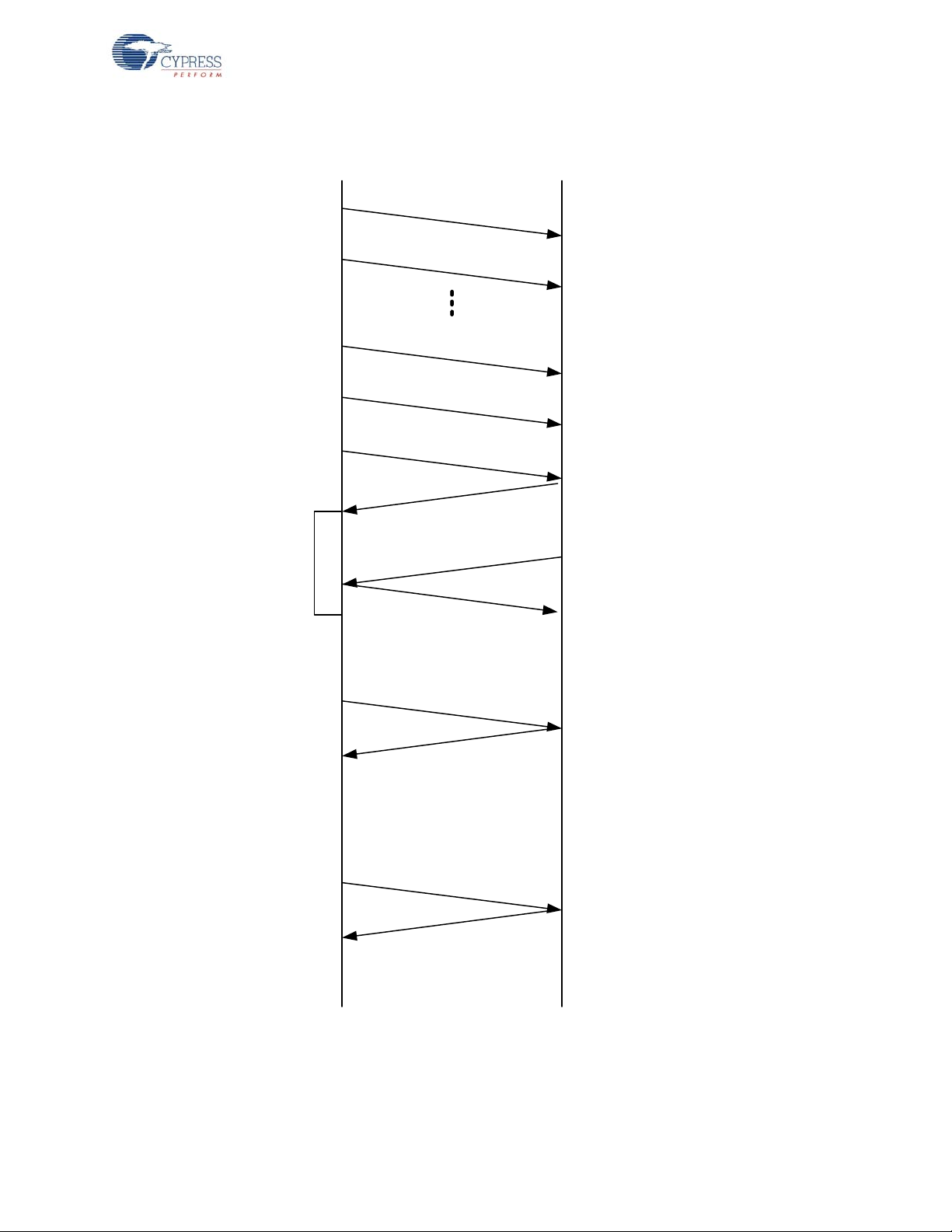
Figure 2-4. KISSBind Transaction Sequence
Master
Slave
KISSBind Request
Ch N, PN 1
KISSBind Response
Connection
Request
Auto ACK
Auto ACK
R
X
KISSBind Request
Ch N + 1, PN 1
Master is in the
connected state on
Ch N+2 PN 3
KISSBind Request
Ch N, PN 3
KISSBind Request
Ch N + 1, PN 3
KISSBind Request
Ch N + 2, PN 3
Auto ACK
Master responds
only if a device of
this type is not
already bound
Master records this
device as being
connected in
FLASH
Data
Auto ACK
Normal traffic
WirelessUSB™ Protocol 2.2
CY4672 Reference Design Guide, Document # 001-16968 Revision ** 19
[+] Feedback
Page 20

WirelessUSB™ Protocol 2.2
2.2.6 Unbind
An ‘unbind’ mechanism allows the bridge and HIDs to return to their default unbind mode as if they
had never bound to any system before.
The bridge dedicates a bind flag to each device type that it supports. A bind flag is a 1-bit field in
Flash. Once the bridge has been bound to an HID by either KISSBind or button bin d mechanism, the
bridge sets the corresponding bind flag for that device type and stores the flag in its Flash.
If the bind flag for a particular device type is se t, the bridge treats future KISSBind packets from this
device type as nonfunctional packets.
The bridge unbind process clears all bind flags, and the bridge allows devices to KISSBind.
The HID dedicates a byte in its Flash, called SIGNATURE, to indicate whether or not the HID has
bound to a bridge before. The SIGNATURE is set to 0x90 after a successful KISSBind or button
bind. If the SIGNATURE is not set to 0x90, the HID tries to KISSBind to any bridge in the area that
allows the HID to KISSBind. Once the SIGNATURE is set, the HID does not attempt to KISSBind.
Note Once the HID enters unbind mode, p ower-cycle the HID to exit this mode. Once the bridge is
unbound, the bridge continues to communicate with any HID that already has the bridge MID. In
order to completely unbind the system, the HIDs and bridge must be unbound.
2.2.7 Data Mode
HID
When the HID application has data to send to the bridge the HID transmits a DATA packet and listens for an AutoACK. If an AutoACK is not received, the HID retransmits the packet. If the HID does
not receive an AutoACK after N DATA_PACKETS_RETRIES of retransmissions of the data packet it
assumes the channel has become unavailable due to excessive interference and moves to reconnect mode.
Bridge
Data mode allows application data to be transmitted from the HID to the bridge. The bridge continuously listens for data packets from the HID. When valid data is received from the HID the bridge
sends an ACK to the HID and sends the data to the USB host. If invalid data is received the bridge
ignores the packet and listens for the HID to retransmit the data. The bridge monitors the interference level and moves to ping mode if the RSSI interference threshold RSSI_NOISE_THRESHOLD
is reached. This ensures that the bridge is operating on a clean channel.
2.2.8 Back Channel Data Support
Back channel data support provides a mechanism for the host to send data to the device at the
request of the device. The device is responsible for interrogating the bridge for back channel data
either as part of a forward data p acket or a simp le null p acket. The device st art s by setting the BCDR
bit in the data header. If the packet is successfully acknowledged by the bridge then the device
inverts the upper byte of the checksum seed an d the n wait for N ms before tr yin g to receive from th e
bridge for M ms. The bridge also inverts the checksum seed and wait N ms before attempting to
transmit to the device. If the bridge has more data to send then it can also set the BCDR flag and can
then expect the device to receive another packet.
20 CY4672 Reference Design Guide, Document # 001-16968 Revision **
[+] Feedback
Page 21
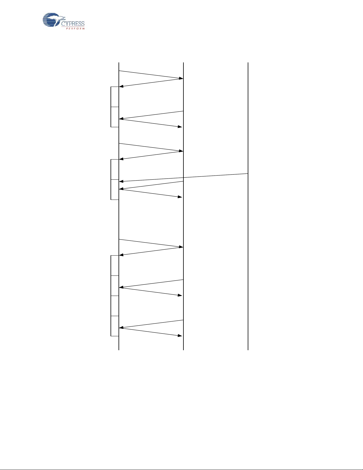
Figure 2-5. Back Channel Transaction Sequence
Bridge
Device 1
Device 2
BCD=1
Auto ACK
Data
CRC Seed = A,A
CRC Seed = !A,A
CRC Seed = A,A
CRC Seed = !A,A
BCD=1
CRC Seed = A,A
CRC Seed = A,A
CRC Seed = !A,A
CRC Seed = A,A
Device 1 and
bridge do not
respond to device
2 due to seed
missmatch
Data
CRC Seed = !A,A
BCD=1
D
e
l
a
y
R
X
Data
CRC Seed = A,A
CRC Seed = !A,A
CRC Seed = A,A
CRC Seed = !A,A
Data
CRC Seed = !A,A
CRC Seed = !A,A
BCD=1
Device 1 checks
for back channel
data
Device 2 transmits
when device 1 is
looking for back
channel data
Dongle indicates
that it has more
data to send
Auto ACK
Auto ACK
Auto ACK
Auto ACK
Auto ACK
Auto ACK
R
X
R
X
R
X
D
e
l
a
y
D
e
l
a
y
D
e
l
a
y
WirelessUSB™ Protocol 2.2
CY4672 Reference Design Guide, Document # 001-16968 Revision ** 21
[+] Feedback
Page 22

WirelessUSB™ Protocol 2.2
2.2.9 Dynamic Data Rate and Dynamic PA
Dynamic data rate and dynamic PA provide the ability to improve the immunity to interferenc e and
reduce power consumption. Dynamic data rate is device be havior based and two d ata mod es, GFSK
and 8DR, are used for the data transmission. Depending on the retry number of prior packets, the
protocol determines whether to stay with the current data mode or change to another data mode.
The dynamic PA relies on both the behavior and the bridge signal strength to the device.
HID
Dynamic Data Rate
If the HID fails to transmit either the application or protocol data to the bridge after
DATA_PACKET_RETRIES of retransmissions, it will toggle data modes and transmit again. If the
HID still fails after DATA_PACKET_RETRIES of retransmissions, it assumes the channel has
become unavailable due to excessive interference and moves to reconnect mode.
If the HID transmits application data successfully, the retries for PKT_NUM packets are summed up
in ‘total_retry’. If the total_retry exceeds the threshold ‘total_retry_threshold’, the HID changes to
another data mode.
The total_retry_threshold is an adaptive number that has a minimum value of
TOTAL_RETRY_THRESHOLD_LOW . The following rules are applied to it:
■ When the data mode is toggled, the total_retry for the previous data mode will be used as current
total_retry_threshold.
■ If the total_retry is zero, the total_retry_threshold will be decreased one until
TOTAL_RETRY_THRESHOLD_LOW.
Dynamic PA
If the total_retry is zero and the RSSI reading for the bridge AutoACK packet is above
PA_RSSI_RX_THRESHOLD, the PA is decreased by one until DATA_MODE_PA_MIN.
When one of the following cases occurs, the PA will be set back to its maximum value of
DATA_MODE_PA_MAX:
■ The data mode is toggled.
■ The RSSI reading for the bridge AutoACK packet is equal to or below
PA_RSSI_RX_THRESHOLD.
■ The retries for any packet exceeds PA_RETRY_THRESHOLD.
Bridge
The bridge does not need to implement the dynamic PA because it is bus powered. Its PA is always
set to the maximum value DATA_MODE_PA_MAX in order to get the highest transmission power.
The dynamic data rate is driven by the devices. When the bridge receives the packet, it sets the
transmission data mode to the data mode of received packet. As a result, when it sends the back
channel data, it uses the same data mode as the device.
22 CY4672 Reference Design Guide, Document # 001-16968 Revision **
[+] Feedback
Page 23

2.3 Packet Structures
The first byte of each packet is the Header byte. Some packets may consist only of the header byte
while other packets may contain up to five bytes.
Byte 1
Bits: 7:4 3:0
Field:
Type[7:4]: The following packet types are supported:
Packet
Type
Reserved
BIND_REQ (HID) = 0x0, // Bind Request Packet Type
BIND_RESP (bridge) = 0x0, // Bind Response Packet Type
CONNECT_REQ = 0x1, // Connect Request Packet Type
CONNECT_RESP = 0x2, // Connect Response Packet Type
PING_PACKET = 0x3, // Ping Packet Type
DATA_PACKET = 0x4, // Data Packet Type
WirelessUSB™ Protocol 2.2
BACK_CHANNEL_PACKET = 0x5, // Back Channel Packet Type
NULL_PACKET = 0x7, // Null Packet Type
ENCRYPT_KEY_REQ = 0x8, // Key Packet Type for encryption
ENCRYPT_KEY_RESP = 0x8, // Key Packet Type for encryption
KISS_BIND_REQ = 0xD, // KISSBind request
KISS_BIND_RESP = 0xD, // KISSBind response
Res[3:0]: The lower nibble is used for packet specific information. The packet definitions below
define how these four bits are used in each case.
2.3.1 Bind/KISSBind Request Packet (HID)
Byte 1
Bits: 7:4 3 2.1 0
Field: 0/0D Reserved
Byte 1
Packet Type: 0 for bind request and 0xD for KISSBind request.
Device Type: This is a 2-bit field that specifies a vendor-defined device type. This allows the bridge
to determine HID type.
Device
Type
Reserved
Currently the following device types have been defined in the PRoC™ LP RDK:
0x0 Presenter
0x1 Reserved
0x2 Keyboard
0x3 Mouse
CY4672 Reference Design Guide, Document # 001-16968 Revision ** 23
[+] Feedback
Page 24
WirelessUSB™ Protocol 2.2
2.3.2 Bind Response Packet (Bridge)
Byte 1 2 3 4 5
Bits: 7:4 3 2:1 0 7:0 7:0 7:0 7:0
Field: 0 Reserved Device
Type
Byte 1
Packet Type: 0 for bind request, 0xD for KISSBind request
Device Type: This is a 2-bit field that specifies a vendor-defined device type. This allows the bridge
to determine HID type.
Currently the following device types have been defined in the KBM RDK:
0x0 Presenter
0x1 Reserved
0x2 Keyboard
0x3 Mouse
Byte 2-5
Reserved Bridge
MID1
Bridge
MID 2
Bridge
MID 3
Bridge
MID 4
Manufacturing ID (MID 1–MID 4): This is the 4-byte manufacturing ID retrieved from the bridge’s
radio and will be used by the HID.
2.3.3 Connect Request (HID)
Byte 1 2 3 4 5
Bits: 7:4 3 2:1 0 7:0 7:0 7:0 7:0
Field: 1 Reserved
Device
Type
Reserved
Byte 1
Device Type: 0x1
Byte 2-5
Manufacturing ID (MID 1–MID 4): This is the 4-byte MID that was received from the bridge durin g the
bind procedure. This enables the bridge to identify if the HID belongs to its network.
2.3.4 Connect Response Packet (Bridge)
Connect response packets are sent from the bridge to the HID in Idle and data mode in response to
valid connect requests.
Byte 1
Bits: 7:4 3 2:0
Field: 2 Flag Reserved
Bridge
MID 1
Bridge
MID 2
Bridge
MID 3
Bridge
MID 4
Byte 1
Packet Type: 2
Flag (F): This is a 1-bit field that specifies a positive or negative connect response packet
(1 = positive, 0 = negative).
24 CY4672 Reference Design Guide, Document # 001-16968 Revision **
[+] Feedback
Page 25
2.3.5 Ping Packet (Bridge)
Byte 1
Bits: 7:4 3:1 0
Field: 3 Reserved Flag
Byte 1
Packet Type: 3
Flag (F): This is a 1-bit field that specifies a ping or ping response (0 = Ping, 1 = Ping Response).
2.3.6 Data Packet/Back Channel Data Packet (Bridge and HID)
Data packets are sent from the HID to the bridge in connected mode. They are als o sent from the
bridge to the HID in connected mode if there is an asynchronous back channel.
Byte 1 2 .. .. N
Bits: 7:4 3 2 1 0 7:0 7:0 7:0 7:0
Field: 4 / 5 BCDR Toggle DT0 DT1 Byte 1 Byte N
WirelessUSB™ Protocol 2.2
Byte 1
Data Packet Type:
4 = Data Packet type
5 = Back Channel Packet Type
BCDR: This is a 1-bit field used to request back channel data. Setting this bit indicates to the bridge
that the HID will be listening for data following the transaction.
Data Toggle Bit: This is a 1-bit field that is toggled for each new da ta packet. It is used to distinguish
between new and retransmitted packets.
Data Device Type 0/1: This is a 2-bit field that specifies a vendor-defined device type. This allows the
bridge to determine HID type. The two bits are swapped in order to be backward compatible. In most
cases the data device type is the same as the device type in the bind request and connect request.
However, they may differ when one device tries to simulate the other device, for instance, the keyboard simulates the mouse.
DT0=0, DT1= 0 Presenter (0x0)
DT0=1, DT1= 0 Undefined (0x1)
DT0=0, DT1= 1 Keyboard (0x2)
DT0=1, DT1= 1 Mouse (0x3)
Byte 2-N
Data Byte 0–N: This is byte-aligned application data.
CY4672 Reference Design Guide, Document # 001-16968 Revision ** 25
[+] Feedback
Page 26

WirelessUSB™ Protocol 2.2
2.4 Bind and Reconnect Timing
When the bind button on the bridge is pressed, the bridge goes into bind mode. In bind mode, the
bridge uses the bind ID to communicate with any HIDs that want to bind to the system (see section
Button Bind Mode on page 17 for more information on the bind ID). The bridge enables its receiver
and ‘listens’ for any bind request packets from the HID, starting from channel 0. The bridge listens for
approximately 320 ms on the channel, and if there is no bind request packet, it moves to the next
channel in the bind channel subset (the bind channel subset consists of channels 0, 6, 12, 18, 24 …
78). It takes the bridge approximately 4.16 seconds to sequentially ‘listen’ on all 13 channels of the
bind channel subset. The bridge repeats the process for up to five times before it times out and exits
bind mode (time out is approximately 21 seconds). If it receives a valid bind request packet, it immediately responds to the request with a bind response packet and exit the bind mode.
When the bind button on the HID is pressed, the HID goes into bind mode. While in bind mode, the
HID also uses the bind ID to communicate with the bridge. The HID sends a bind request packet and
listens for an AutoACK packet. If the HID does not receive the AutoACK, it moves to the next channel in the bind channel subset and repeats the bind request packet. It takes the HID approximately
23.4 ms to sequentially hop through all 13 channels of the bind channel subset, and the HID repeats
the process for up to 1000 times before it times out. Refer to Figure 2-6 Bind Timing Diagram.
Because the bridge’s and HID’s bind buttons may be pressed at different times, the HID and the
bridge could be on very different chan nels when the two are in bind mode . However, because the
HID ‘hops’ very quickly on all bind channels while the bridge stays relatively long on a channel, the
bridge and HID will have multiple opportunities of being on the same channel. As a result, binding
normally completes very quickly as soon as the bridge and the HID are both in bind mode (at 1.8 ms/
channel ‘hopping’ frequency of the HID and the bridge’s 320 ms/channel, the two will ‘meet’ on the
same channel at least 13 times in any 320 ms period).
26 CY4672 Reference Design Guide, Document # 001-16968 Revision **
[+] Feedback
Page 27
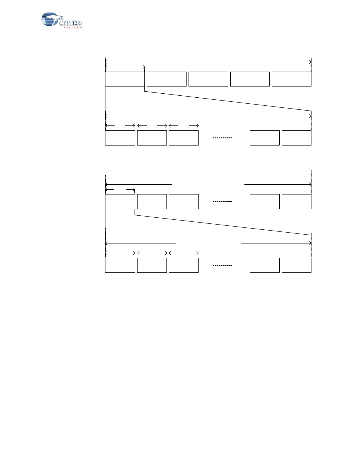
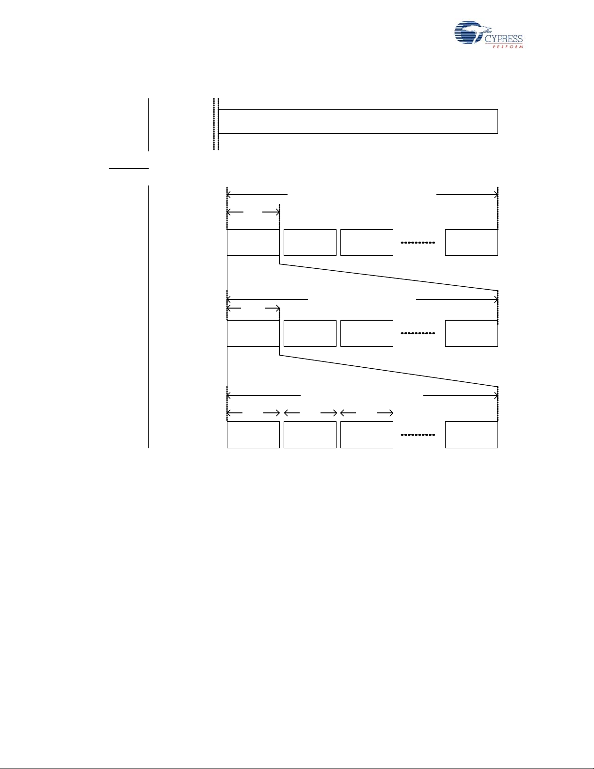
Figure 2-6. Bind Timing Diagram
Cycle 1 Cycle 2 Cycle 3
23 .4 m s
Cycle 1000
23.4 ms x 1000 Cyles = 23.4 seconds
Bridge
Device
Channel 0 Channel 6 Channel 12 Channel 78
1.8 ms 1.8 ms 1.8 ms
1.80 ms x 13 Channels = 23.4 ms
Cycle 1 Cycl e 2 Cycle 3 Cycle 4 Cycle 5
4.16 s
4.16s x 5 Cycles ~ 21 seconds
Channel 0 Channel 6 Channel 12 Channel 72
320 ms 320 ms 320 ms
320 ms x 13 Channels ~ 4.16 seconds
Channel 78
Cycle 999
Channel 72
WirelessUSB™ Protocol 2.2
The bridge uses the RSSI to determine the noise level on the channel. If the channel has become
noisy, the bridge moves to ping mode to find a quieter channel in its channel subset.
HID sends a connect request packet and liste ns for an AutoACK packet. If the HID receives the
AutoACK, it immediately enables its receiver and listens for the connect response packet from the
bridge. If the HID does not receive the AutoACK it selects the next channel using the channel selec-
When the HID loses connection with the bridge, it moves to reconnect mode to find the bridge. The
tion algorithm and repeats this procedure. As shown in the reconnect timing diagram below, the
reconnect attempt takes approximately 1.76 ms/channel. Th e HID mo ves thr ou gh its channel subset
up to 19 times before it times out and exits reconnect mode. The keyboard tries to send the data for
up to five seconds, and the mouse tries for two seconds, causing the HID to re-enter reconnect
mode multiple times if necessary.
CY4672 Reference Design Guide, Document # 001-16968 Revision ** 27
[+] Feedback
Page 28
WirelessUSB™ Protocol 2.2
Reconnect
Mode
Reconnect
Mode
Reconnect
Mode
430 ms
Reconnect
Mode
Keyboard = 5 seconds; Mouse = 2 seconds
Inherence detected .
Move to a quieter
channel in the subset
Quiet channel found. Bridge will stay on this channel
Device lost connection .
Search for bridge in
the channel subset
Cycle 1 Cycle 2 Cycle 3 Cycle 19
22 .88 m s
22.88 ms x 19 Cycles ~ 430 ms
1st Channel
in subset
2nd Channel
in subset
3th Channel
in subset
13th Channel
in subset
1 .76 m s 1.76 ms 1 .76 m s
1.76 ms x 13 Channels = 22.88 ms
Bridge
Device
Figure 2-7. Reconnect Timing Diagram
2.5 Signature Byte
The PRoC LP RDK uses the Signature byte to determine if the HID has ever been bound to any
bridge before.
If the HID has never bound to a bridge, the non-volatile memory used to store the signature and the
bridge's MID data remains in its default value. Once the HID has bound to a bridge, the Signature
byte is set to 0x90 and the bridge's MID is also stored.
At power up, the HID reads the Signature and the MID bytes to determine its next action. If the Signature byte is 0x90, the HID uses the retrieved MID to calculate the networkID and moves to Reconnect mode. If the Signature byte is not 0x90, the HID goes to sleep, waiting for the user to initiate
the bind process.
28 CY4672 Reference Design Guide, Document # 001-16968 Revision **
[+] Feedback
Page 29

2.6 Encryption
WirelessUSB PRoC LP RDK supports Tiny Encryption Algorithm (TEA) and Advanced Encryption
Standard (AES) 128 to encrypt application data. Data packets may be encrypted for privacy. All
encrypted data packets must have a payload of 8 or 16 bytes depending on the method chosen; this
is the minimum block size for the encryption algorithm.
2.6.1 TEA Encryption
Some of the features of TEA are:
■ 128-bit encryption key
■ 8-byte block size
■ Minimal RAM requirements
■ Small code size
■ Highly resistant to differential crypt analysis
In order to use the TEA algorithm both the bridge and HIDs must possess the data encryption key.
The bridge is responsible for creating the key, which is then shared with the HIDs. There are a variety of possible methods to share the key between the two devices. The key may be exchanged over
the WirelessUSB link using the encryption key request and encryption key response packets.
WirelessUSB™ Protocol 2.2
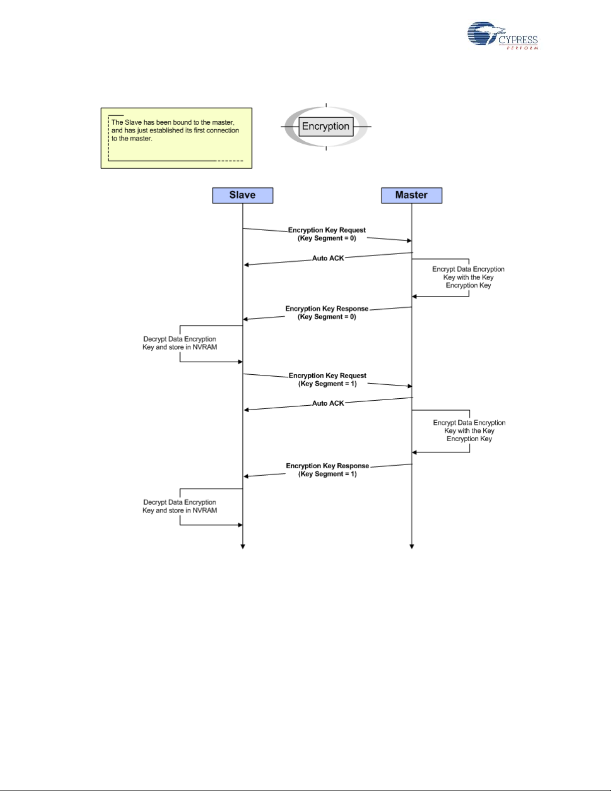
2.6.1.1 TEA Key Management over WirelessUSB
After binding and connecting to the bridge, the HID transmits an encryption key request packet and
listens for an AutoACK followed by an encryption key response packet that contains the first half of
the data encryption key. The HID then uses the key encryption key (calculated from the bridge and
the HID MIDs) to decrypt the data encryption key. The HID repeats this process for the second half
of the data encryption key and stores the key in Flash. After rece iving both halves of th e data e ncryption key the HID may begin transmitting encrypted data to the bridge.
CY4672 Reference Design Guide, Document # 001-16968 Revision ** 29
[+] Feedback
Page 30
WirelessUSB™ Protocol 2.2
Figure 2-8. TEA Encryption Key Management
2.6.2 AES Encryption
AES_Encrypt requires the two variables tx_packet and AES_Key to be set prior to the call. Each
contains a 16 byte (128 bit) value. At the completion of the function tx_packet ha s been encrypted inplace and contains the cipher text. AES_ Key is scheduled in- place during the e ncryption process, so
multiple calls to AES_Encrypt will each need to be proceeded with reloading of AES_Key.
AES_Decrypt is the same as the AES_Encrypt; rx_packet and AES_Key both need to be loaded
prior to each call. However there is one small difference (because the decrypt key schedule is in
reverse order), the decryption key is not the same as the encryption key. The key used by
AES_Decrypt is the same as the key left in the AES_Key field after an execution of AES_Encrypt.
This is the key after it has gone through ten rounds of Key scheduling.
30 CY4672 Reference Design Guide, Document # 001-16968 Revision **
[+] Feedback
Page 31

2.6.2.1 AES Key Management
The encrypt key is stored on the keyboard and the decrypt key is stored on the br idge dur ing compiling time. There is no dynamic encrypt key exchange in the running time.
2.6.3 Encryption and Power Consumption Trade Off
If the keyboard encryption is enabled, each key code is encrypted into an 8 byte key code (TEA) or
16 byte key code (AES). When a single key is pressed, a non-encrypted key down packet consists of
a 16-bit Preamble + 2 bytes SOP + 1 byte packet header + 1 byte key code + 2 bytes CRC; an
encrypted key down packet consists of the same overhead packets plus 8 or 16 byte key code
instead of one byte key code. This results in an increase in the average power consumption when
encryption is enabled.
WirelessUSB™ Protocol 2.2
CY4672 Reference Design Guide, Document # 001-16968 Revision ** 31
[+] Feedback
Page 32

WirelessUSB™ Protocol 2.2
32 CY4672 Reference Design Guide, Document # 001-16968 Revision **
[+] Feedback
Page 33

3. Mouse
3.1 Introduction
This section describes the design goals, architecture, firmware source code modules and configuration options for the PRoC™ LP mouse. It does not cover the details of the radio subsystem or the
configuration options that go with it.
3.1.1 Design Features
The CY4672 Reference Design Kit uses a low cost PRoC LP for the RDK mouse (Cypress p art number CYRF69103). Contact your local sales representative for more information.
The architecture was designed to be modular for extendibility and maintainability. It was also
designed so that it could easily be ported from one hardware platform to another assuming the use
of an equivalent microprocessor. Porting to another microprocessor family requires more work to
account for hardware specific changes.
Design efforts have been made to reduce the ‘on’ time of the microprocessor and radio to conserve
battery life. This includes protocol optimizations along with using sleep features of the PRoC LP and
optical sensor.
3.2 Hardware Overview
The mouse assembly, hardware block diagram, schematic, and hardware considerations are discussed in this section.
3.2.1 RDK Mouse Assembly
The PRoC LP RDK mouse is currently enclosed in a skin that has been designed for the Avago
ADNS-3040 Ultra Low-Power mouse sensor. The mouse features three buttons with one button
combined with the scroll wheel function. There is a connect button on the bottom of the mouse allowing the user to perform an explicit bind with the bridge.
CY4672 Reference Design Guide, Document # 001-16968 Revision ** 33
[+] Feedback
Page 34

Mouse
Figure 3-1. Bottom View Bind Button and On-Off Switch
Figure 3-1 shows the bottom of the mouse with the optics window, power switch, and Bind button.
There are two screw holes above the label. The top of the mouse can be removed once these two
screws on the bottom and one screw on the top have been extracted.
Figure 3-2. Exploded Mouse View
Figure 3-2 is a picture of the mouse with the top removed. The mouse consists of a single PCB that
contains all of the necessary mouse components.
34 CY4672 Reference Design Guide, Document # 001-16968 Revision **
[+] Feedback
Page 35

3.2.2 Hardware Block Diagram
PRoC Optical sensor
SPI
O_nCS
Scroll Wheel
Buttons
O_Motion
Figure 3-3. Mouse Hardware Block Diagram
3.2.3 Schematics
All schematics for the optical wireless mouse are located in the following directory: <installation
directory>\Hardware\Mouse. The schematic is in Adobe Acrobat format with the letters ‘Sch’ in the
file name.
Mouse
Figure 3-4. Printed Circuit Assembly (PDC-9347)
Figure 3-4 is a picture of the controller board with the PRoC LP and optical sensor. The ‘wiggle’ trace
in the upper left is the antenna. This board has the option of adding pull up resistors and filtering
capacitors to the z-wheel and then powering the z-wheel with a separate GPIO pin on the microcontroller. J1 0 is a programming h eader. Either the ICE-Cube or the PSoC MiniProg may be used to program the mouse microcontroller using this ISSP header. J10’s pin 1 is a double header as a
mechanism to isolate the programming voltage and the operating voltage. To enter a manufacturing
CY4672 Reference Design Guide, Document # 001-16968 Revision ** 35
[+] Feedback
Page 36

Mouse
test mode that is compatible with the Cypress Manufacturing Test Kit, use a shorting block and short
together pins 4 and 5 before power is applied.
3.2.4 Hardware Considerations
The mouse design uses the SS12 schottky diode (D1) and CDH53100LC inductor (L3) for its boost
circuitry. With these high efficiency components, preliminary characterization data shows a range of
approximately 74-87% efficiency for the 1.8-2.7V VBAT voltage range at different temperatures
(-10C to 80C). The mouse is a higher power consumption device compared to the keyboard. Extending the battery life is one of the crucial design considerations in the mouse design. The trade off for a
higher efficiency boost circuitry is the component costs and the board size (these components are
slightly bigger in size compared to the ones used in the keyboar d design). T hese comp onent s do n ot
provide enough current capacity at the low end of the VBAT voltage range to handle the worst case
optical sensor load and the PMU output voltage may droop under these conditions. The recommendation is to use an external DC/DC boost circuit for the optical system only.
3.3 Firmware Architecture
There are two architectural views of the mouse. The first is a microcontroller configuration view. This
architecture and configuration is best viewed in the PSoC Designer™ application when the project is
loaded. The second view is a logical organization of the source code modules that make up the
mouse application code and other support modules.
This section describes both architectures with emphasis on top level organization and overall module operation. More detailed description of variables and functions should be obtained by studying
the source code.
3.3.1 ROM/RAM Usage
The following table shows the ROM/RAM usage. The top part exhibits the total ROM/RAM usage for
basic functions, which disables all the build options below. The bottom part exhibits the ROM/RAM
usage for individual build options.
Table 3-1. ROM/RAM Usage
Basic Function 5334 70
Build Option ROM Usage (Bytes) RAM Usage (Bytes)
MOUSE_BATTERY_STATUS 255 2
MOUSE_TEST_MODE 537 0
MFG_TEST_CODE 530 0
MFG_TX_MODES 755 2
3.3.2 PRoC LP Device Configuration
Total ROM (Bytes) Total RAM (Bytes)
The PRoC LP Programmable Radio on Chip is configured using the Device Editor in PSoC
Designer. The mouse u ses 2 digit al blocks to supp ort two sep arate user module s. The first module is
an SPI master for communicating with the optical sensor and the radio. The second modu le is a Programmable Interval Timer configured to operate as a 12-bit timer. The following is a screen shot of
36 CY4672 Reference Design Guide, Document # 001-16968 Revision **
[+] Feedback
Page 37

Mouse
the Device Editor showing the user module mapping. Further description of resources and user
modules follow the diagram.
Figure 3-5. CYRF69103 Device Architecture
CY4672 Reference Design Guide, Document # 001-16968 Revision ** 37
[+] Feedback
Page 38

Mouse
3.3.2.1 Global Configuration
Following is a description of the Global Resources that are configured for the CYRF69103 PRoC
LP Programmable Radio on Chip. Care must be taken when modifying these values as they affect
the user modules discussed below.
3.3.2.1.1 CPU Clock This parameter is set to Internal (24 MHz). In order to run the CPU at 12 MHz, CPU Clock/N needs
to be set to ‘2’. This operating frequ ency prov ides for faster code execution so that when events are
detected the microcontroller can be put back into the sleep state quicker for improved power savings.
3.3.2.1.2 CPU Clock / N This parameter is set to ‘2’ to provide a 12 MHz clock.
3.3.2.1.3 Timer Clock This parameter is set to FreeRun Timer.
3.3.2.1.4 Timer Clock /N This parameter is set to ‘4’.
3.3.2.1.5 FreeRun Timer This parameter is set to Low Power (32 kHz).
3.3.2.1.6 FreeRun Timer /N This parameter is set to ‘6’.
3.3.2.1.7 Capture Edge This parameter is set to Latest.
3.3.2.1.8 8 Bit Capture Prescaler This parameter is set to ‘1’.
3.3.2.1.9 CLKOUT Sour ce This parameter is set to Internal (24 MHz).
3.3.2.1.10 Low V Detect This parameter is set to 2.63V–2.68V.
3.3.2.1.11 V Reset This parameter is set to 2.6V.
3.3.2.1.12 Watchdog Enable This parameter should be set to Enable, but may be set to Disable for debug purposes.
3.3.2.2 SPI Master User Module
The SPI Master User Module is used to com m uni ca te with bo th th e r ad io t ra ns ceiver and the optical
sensor. Both devices support leading edge data latching, non-inverted clock and MSB first transmission as defaults. A clock divisor of 12 is chosen which generates an SPI clock of 1 MHz. The inter-
38 CY4672 Reference Design Guide, Document # 001-16968 Revision **
[+] Feedback
Page 39

rupt API to this module is not used. See the SPI Module on page 40 for how this module is used to
debounce spi
flash radio driver
protocol
poll
timer
isr
mouse optical
testmode
mfgtest
battery
buttons
wheeltick
GPIO
Common
PSoC Lib
Application
implement communication with multiple devices on the SPI bus.
3.3.2.3 Programmable Interval Timer User Module
The Programmable Interval Timer User Module is configured to use the Internal 32-KHz Low-power
Oscillator. This module is used to provide a periodic interrupt to the timer code module in order to
maintain a power saving millisecond sleep routine. The period of the timer is calibrated to the system
clock at power on in order to provide a period of about 250 µs. This calibration is performed to
account for variations in temperature and ILO variances from part to part. Configured the module to
generate a terminal count interrupt. The period parameter is ignored since it is programmed at run
time based upon the calibration results. See the Timer Module on page 41 for more details on cali-
bration
3.3.2.4 Flash Security
The PSoC Designer mouse project has a file called FlashSecurity.txt. This file specifies access rules
to blocks of the Flash ROM. Refer to the documentation at the top of the file for definitions. This file
is shipped with a single change from its default configuration. The block starting at hex address
1FC0 has been changed from W: Full (Write p rotected) to U: Unprotected. This location of Flash has
been dedicated to saving non-volatile configuration values for the protocol code module (refer to the
Protocol Module on page 41).
text image size does not occupy this block.
Note When building the mouse firmware, be sure to check that the
Mouse
3.3.3 Model
Figure 3-6. Firmware Architecture Model
CY4672 Reference Design Guide, Document # 001-16968 Revision ** 39
[+] Feedback
Page 40

Mouse
The mouse firmware is partitioned in to two logica l group s. The Commo n group is a collection of code
modules that provide the underlying support for the application. This group provides services such
as radio protocol, radio driver, timing, polling, flash access, contact debounce, SPI, and interrupts.
The Application group implements the core functionality and features of the PRoC LP RDK mouse.
This includes power management, optical sensor, button, z-wheel, packet formatting and reporting,
various test modes and battery level sensing. The code modules for each of these groups are
described below in further detail.
All of the following module descriptions have corresponding <module name>.c or <module
name>.asm and <module name>.h source code files. The module API and definitions are exported
in the header file while the module implementation and local definitions are contained in the C/
assembly file.
3.3.4 Common Code
The modules in the common code group are a combination of two sources. The first is PSoC
Designer generated files in the
second group is modules that are generally used by the application.
3.3.4.1 Generated Library Code
There is currently only one file, generated by PSoC Designer, that is modified for the use of the
application. A minimal amount of code has been added to this module in user protected areas that
are preserved across code generatio n.
lib directory that have been modified to support the application. The
3.3.4.1.1 Timer Interrup t Mo du le The timer interrupt module has been modified to provide a finer timing of 250 µs for the Poll Module
and course timing by providing a 1 ms tick. When the timer module has been turned off, it still provides a sense of time on the 1 ms tick by using the sleep timer . In this case po lling is disabl ed to conserve power . See the Poll Module on page 41 and the Timer Module on page 41 for more details.
3.3.4.2 Debounce Module
The debounce module is an assembly coded routine to perform deb ounce on bu tton pr esses as we ll
as z-wheel motion. The algorithm is one that was publ ish ed in EDN article as a way to per form hardware debounce in software.
The debounce is performed by polling the inputs at a fixed period and by adding a weighted value of
the input to an accumulated value carried from the previous poll. The output is then passed to
threshold logic, with built in hysteresis, and a logic value of one or zero is computed. The thresholds
can be changed to adjust the hysteresis crossings by setting SCHMITT_HIGH_THRESH and
SCHMITT_LOW_THRESH. Once an input has changed state, the output can be observed to
change approximately 10x the poll period later with the current threshold settings. With a poll period
of 250 µs the input latency is about 2.5 ms.
Refer to
details on the operation of this algorithm.
Contact-debouncing algorithm emulates Schmitt trigger at http://www.edn.com for more
3.3.4.3 SPI Module
This module provides an interface to the SPI bus for the optical sensor only . Physically the SPI bus is
connected to the radio and the optical sens or. The radio driver is responsible for inter facing with the
radio. The PRoC LP SPI Master module does not manage the selection of slave devices. This module was created to provide that functionality. This module has a dependency on the instantiation of a
SPIM module in PSoC Designer that is properly connected to the devices.
40 CY4672 Reference Design Guide, Document # 001-16968 Revision **
[+] Feedback
Page 41

In the PRoC RDK mouse design, the master SPI communicates with both the radio and optical sensor. Because th e optical sensor does not suppo rts 3- wire SPI mode, the 4-wire mo de is employed. In
order to save the GPIO pin, the IRQ pin function is multiplexed onto the MOSI pin.
3.3.4.4 Radio Driver
The radio driver module is a low level module providing basic radio communication and configuration. Its general application is such that it is likely not to be changed by the firmware developer. It
provides an interface for reading/writing radio registers, setting PN codes and initialization of the
radio and transmitting or receiving packets. See the PRoC LP Radio Driver documentation for
details.
3.3.4.5 Protocol Module
The protocol module defines and implements the layer used to deliver packets from the device to the
bridge. It manages the binding of devices to a bridge as well as the connection and interference
immunity by channel hopping. This module has a dependency on the Radio Driver for sending for-
matted packets and the flash module for storing the manufacturing ID of the bridge the device is
bound to.
3.3.4.6 Flash Module
The flash module is a smaller version of E2PROM module provided in PSoC Designer. It is limited in
functionality and only implements the read/write routines requ ired by the device. T he
file must be modified so that the block being modified by this module is given read/write privilege,
such as unprotected. Currently the very top most block in flash is used for this module.
Mouse
flashsecurity.txt
3.3.4.7 Port Module
GPIO pins on the PRoC LP ports can be configured as outputs with a pull up resistor. This is the
case for mouse buttons and the Bind button . In order to activate the p ull up, a dat a va lue of one must
be written to the port data latch for the pin. This fe atur e pr esen ts a problem when performing a readmodify-write on the port. For example, if a button is pressed (grounding the pin), a zero is read and
written back out on the read-modify- write operation. This turns off the pull up for th e button ther eby,
essentially disables the button. The port module provides an interface to treat ports, using the pull up
feature, in a special way by caching the drive data for the port.
3.3.4.8 Poll Module
The poll module manages the timing, enabling/disabling and polling of the mouse buttons and zwheel inputs. When the mouse is active, polling is enabled and occurs at a rate of about 250 µs for
the z-wheel (see the Timer Module) and a rate of about 3 ms for the mouse buttons. When the
mouse is inactive, the buttons are changed to interrupt mode and the z-wheel is polled for change
only when the sleep timer expires; see the Buttons Module and Wheel Module on page 44.
3.3.4.9 Timer Module
The PRoC LP has an internal low power oscillator (ILO) that is used for generating a clock to a Programmable Interval Ti mer. This clock is affected by vo ltage and temperature and may drift over time.
This module provides an interface to calibrate this clock to the system clock. The Programmable
Interval Timer period is calibrated to be approximately 250 µs. Be especially careful when changing
this period since the poll/debounce modules are coupled to this time value; see Poll Module and the
Debounce Module on page 40.
The timer module also provides a set of functions for performing busy waits in the microsecond resolution. For more coarse timing requirements, an API is provided for millisecond delays. The millisecond delay routines must be used as often as possible to provide for better power consumption
CY4672 Reference Design Guide, Document # 001-16968 Revision ** 41
[+] Feedback
Page 42

Mouse
since the microcontroller sleep featur e is used. Also, when polling is enabled, it is performed as a
background task during the millisecond delay.
This module also adjusts the tick advancement based upon the sleep resolution. Turning off the
timer provides for more power savings, yet a sense of time is still preserved for non-critical timing.
Note When using the ICE-Cube, define the macro PSOC_ICE so that busy wait s are used instead of
the sleep instruction. Using the sleep instruction with the ICE-Cub e generates er rors due to synchronization issues between the OCD p art and the emulator.
3.3.4.10 ISR Module
This module provides an interface to initialize the interrupt.
3.3.5 Application Code
The group of modules that make up the application code are responsible for implementing the
mouse functionality and behavior. Following is a high level description of each module responsibility
and associated algorithms.
3.3.5.1 Mouse Module
The mouse module is the controlling code for the application. It has many responsibilities in implementing various features and functions offered by the mouse. The data formats and reporting algorithms along with power management are explained in this section.
A few format types are defined to support the operation of the mouse. One of these is the packet format used when sending data to the bridge. This type is defined as TX_PACKET and is structured to
support the different data pa cket formats as explained in the section Wireless Protocol Data Payload
on page 47. The present definition combines z-wheel data with button data into one byte in order to
conserve battery power by shortening the ‘on time’ of the radio. This format needs to change in or der
to support a mouse with more than three buttons and a z-wheel, perhaps sending four bytes instead
of three.
The function main() is the entry point for the mouse application. This function is called from the
boot.asm file. The mouse first initializes all of the application modules and then initializes the proto-
col module; see Protocol Module on page 41. There is an order dependency for some of these, so
care must be taken in modifying the mouse_init() function. For example, other modules depend upon
the timer facility running in order to perform initialization. The spi module must be initialized before
the optical and protocol modules can be initialized; see SPI Module on page 40, Optical Module on
page 43 and Protocol Module on page 41. Once each module has been initialized, then the applica-
tion checks for entry to the ‘LP’ draw test mode or the manufacturing test mode. If neither of the te st
modes is indicated, then normal mouse operation begins.
The mouse module handles a variety of events at the main thread level. Most interrupt routines post
notification that an event occurred by using the macros provided by the mouse interface. The mouse
then processes these events at thread context rather than interrupt context.
The mouse application is implemented using a state machine to manage the various power modes
that it executes at any given time.
The mouse initially enters a disconnected state. When there is any mouse activity, it enters the
active state.
In the active state the timer is turned on so that more accurate timing and mouse events can be collected, formatted and reported to the bridge. The mouse remains in this state as long as there is
mouse activity to report to the bridge or a period of time with out any mo use activity has expired, af ter
42 CY4672 Reference Design Guide, Document # 001-16968 Revision **
[+] Feedback
Page 43

Mouse
which it returns to the idle state. If the mouse is unable to deliver a packet while in this state, it transitions to the disconnected state.
In idle state the optical sensor is allowed to transition through its various rest modes to conserve
power. In this st ate, th e mouse application is waiting for input from the op tical sensor, z-wheel or buttons. The timer is turned off to conserve power and the notion of time is maintained using the sleep
timer. This state is maintained indefinitely until the batteries drop below 1.8 volts at which point the
mouse enters the off state.
The off state is where the radio and optical sensor are prevented from turning on. This state is
reached when the battery voltage drop s b elow 1.8 vo lt s. It is de signed to keep the battery dra in to an
absolute minimum to prevent battery leakage as a result of completely draining the batteries.
The battery level is reported by the mouse application when it detects a change from the disconnected state to the connected state. The battery level is measured when exiting the idle state. If
there is a change in the battery level, it will be reported in the active state.
In the active state the mouse attempts to deliver a packet for the amount of time designated in
MOUSE_TX_TIMEOUT_MS. If it is unable to send the packet in this time, then it transitions to the
disconnected state.
The mouse application is responsible for detecting the Bind button press and then calling the bind
function in the protocol module; see Protocol Module on page 41.
The mouse application sends mouse reports as frequently as events arrive, but not any faster than
the time defined in the macro MOUSE_REPORT_IN_MS. Carefully set this time so that the report
rate does not exceed that which the USB bus is capable of handling. Keep in mind that the report
rate varies slightly due to drift of the internal oscillator used to keep track of time.
3.3.5.2 Optical Module
The optical sensor module encapsulates the initialization, calibration and reading of the optical sensor. This module also handles any power management required by the sensor, along with motion
detection if supported. The contents of this module potentially change with every design and are
unique to the sensor used.
This module has the responsibility to format the X and Y data into the mouse packet payload. Refer
to section Wireless Protocol Data Payload on page 47 for a definition of the packet payload.
3.3.5.3 Testmode Module
The Testmode module provides code to continuously perform a vector drawing test within a drawing
application. This test mode is used to check radio range, co-location and interoperability of the
mouse with the keyboard.
The test mode, when compiled in, is entered by holding down the left and rig ht button while inserting
the batteries. The buttons must be held down until the optical sensor begins to flash. As soon as the
buttons are released the mouse repeatedly draws ‘LP’ in the drawing application. Each successive
‘LP’ must be drawn on top of the previous one. The test mode may only be exited by removing the
batteries. All button presses and mouse movement are ignored when in the test mode. However,
care must be taken not to bump other mice connected to the PC.
Note The mouse ‘acceleration’ or ‘enhance pointer precision’ option needs to be turned off in the
Windows mouse Control Panel for this test to execute properly. If the letters are drawn erratically
with uneven sides or excessive amounts of space in between them, then check this setting or its
equivalent (based upon your PC operating system).
When the macro DEBUG_INDEX is defined, code is generated to move the mouse pointer to the
right and back again without the pen down. This is done in an incrementing fashion so that when
CY4672 Reference Design Guide, Document # 001-16968 Revision ** 43
[+] Feedback
Page 44

Mouse
observing packet data on a Listener, a correlation can be made with a USB protocol analyzer. This is
useful for debugging data loss since the test mode guarantees packet delivery.
Entry to this test mode can be changed by modifying the macro TESTMODE_BUTTONS in the test-
mode.c
file. The button macros are defined in the buttons.h file.
3.3.5.4 Buttons Module
The buttons module provides an API for handling both the bind and mouse buttons. This module
must be changed when adding or removing buttons for a new mouse design. The button portion of
the packet payload is formatted by this m odule and needs to change if more buttons are added. See
the Mouse Module on page 42 module for a definition of the packet payload format.
This module manages power configuration s that may be implemente d to conserve power relat ed to
button presses. For example, button polling is turned off and interrupts are used to detect button
presses in the idle state. It also manages the acquisition of button information depending on the
implementation: interrupts or polling.
When changes in a button state are detected, the mouse module is notified fo r collection and reporting of the data.
button is pressed. This condition frequently occurs when the mouse is moved with the button held
down.
Note It is important for the buttons module to always report the button state when a
3.3.5.5 Mfgtest Module
The manufacturing test module may be optionally compiled in, at the expense of code space, by
defining the macro MFG_TEST_CODE. In addition, a more complete version may be compiled in by
defining MFG_TX_MODES. The TX modes include code to perform a carrier test as well as a random data test.
The manufacturing test code is designed to be compatible with the CY3631 Manufacturing Test Kit
Tester. Entry into this mode on the mouse is performed by placing a shorting block over pins four and
five of the ISSP programming header and then inserting the batteries. The test mode may only be
exited by removing the batteries and shorting block. For more information on how to use this test
mode, refer to the CY3631 Manufacturing Test Kit documentation.
It is recommended that you not make changes to this module unless similar changes are made to
the CY3631 Tester.
3.3.5.6 Wheel Module
The wheel module implements the functionality of the z-wheel. It is responsible for pow er modes
associated with the z-wheel, polling, z-wheel interrupts, wheel position tracking, and partial packet
formatting for z-wheel reports.
When the z-wheel is being polled, the GPIO pins are turned on with internal pull up resistors just
long enough to read the state. This is done to conserve power when the mouse is active. When the
polling timer has been turned off the wheel_poll_sleep() function is called which only looks for
change from the last state; it does not keep track of wheel position.
Z-wheel position tracking is done by comparing debounced wheel input to the previous two states.
Depending upon the wheel input phase transition the direction of the wheel can be determined. The
poll rate must be frequent enough to debounce and catch these transitions for a smooth response.
The RDK mouse is shipped with a mechanical encoder. It is typical for this decoder to rest on a
detent such that the z-wheel inputs are either bo th high or both low, hence the reason for only turning
on the pull ups when polling the input. Transition from one of these states to the other is reported as
a +/-1 motion.
state and movement may not be seen every time from detent to detent.
Note Sometimes the mechanical detents do not align with the high-high or low-low
44 CY4672 Reference Design Guide, Document # 001-16968 Revision **
[+] Feedback
Page 45

When z-wheel motion is detected, the mouse module is notified for collection and reporting of the
data; see Mouse Module on page 42.
3.3.5.7 Battery Module
The battery monitor circuit is implemented using the Low Voltage Interrupt (LVI) on the LP radio. Following is an explanation of the process to measure the battery voltage.
The process first sets the LVI threshold to 1.8V and then checks for an LVI interrupt. If the interrupt
does not occur then it repeatedly se ts the LVI TH and PMU OUTV with the following co mbination
and checks the status.
Table 3-2. LVI TH and PMU OUTV Combinations
LVI TH PMU OUTV VOLTAGE IF INTERRUPT OCCURS
1.8V 2.7V < 1.8V
2.0V 2.7V < 2.0V
2.2V 2.7V < 2.2V
PMU OUTV 2.7V < 2.7V
It then returns a battery level between 1 and 10: 1 being below 1.8V and 10 being above 2.7 volts.
Mouse
3.3.6 Configuration Options
All configuration options for the application can be found in the config.h file, and some of them are
defined in the Project > Setting > Compiler > Macro defines. Each option is explained below and can
be changed to values that meet the developer’s needs.
3.3.6.1 MOUSE_REPORT_IN_MS
This configuration value sets the shortest period at which the firmware honors events from the
mouse hardware to transmit using the radio. The default value is approximately 10 milliseconds. Setting this value to something smaller than the USB poll period of 8 milliseconds generates excessive
radio retries from the mouse and is not recommended. Larger values improve battery life, but may
affect usability of the mouse. See the Timer Module on page 41 for a description of timing accuracy.
This valued is defined in milliseconds.
3.3.6.2 MOUSE_ACTIVE_MS
This value sets how long the timer module runs generating poll interrupts for the z-wheel and buttons. This time affects power consumption of the mouse. Once this time expires, the buttons and zwheel go into a power down state, improving battery life. In power down state, z-wheel movement
exhibits latency. See the Buttons Module and Wheel Module on page 44 for descriptions of power
down states and operation. This value is defined in milliseconds.
3.3.6.3 MOUSE_DISCONNECTED_POLL_MS
Sets the rate at which the battery voltage is monitor ed while in the dis conn ected state. T his ensu res
that if the batteries go below the minimu m battery voltage of 1.8 V, the radio and optical sensor are
prevented from turning on.
3.3.6.4 MOUSE_TX_TIMEOUT_MS
The transmit loop in the mouse attempts to guarantee de livery of mouse event s. This l oop eventu ally
times out if it does not receive a response from the bridge. This value sets that time-out time. The
default value is 2000. This value is defined in milliseconds.
CY4672 Reference Design Guide, Document # 001-16968 Revision ** 45
[+] Feedback
Page 46

Mouse
3.3.6.5 MOUSE_CONNECT_ATTEMPT_TIMES
This value sets the attempt times for the mouse trying to connect to the bridge before entering the
Briefcase Mode. The default value is 20.
3.3.6.6 PLATFORM_H
This configuration value identifies the header file that has the platform configuration in form ation. Th e
default value is
This macro changes when the code is ported to another plat form.
pdc9347.h, which is the identifier for the mouse board that is shipped with the RDK.
3.3.6.7 MOUSE_800_NOT_400_CPI
This configuration definition is used to select between 800 or 400 counts per inch (cpi) when configuring the optical chip. If it is defined then 800 cpi is selected. If it not defined then 400 cpi is selected.
The default is 800 cpi.
3.3.6.8 MOUSE_BATTERY_STATUS
Enabling this feature causes the battery level measurement code to be compiled into the mouse
image. The mouse then measures the battery level and reports any changes to the bridge. Notification of the battery level is done at the following events: the battery level changes, the mouse transitions from the idle state to the active state, mouse transitions from the disconnected state to the
connected state.
3.3.6.9 MOUSE_TEST_MODE
This configuration definition is used to selectively compile code for mouse test mode. If this value is
defined, then the test mode is compiled into the executable image.
The test mode moves the mouse in a fashion to repeatedly draw the letters ‘LP’ in a drawing program. When performing this test, turn of f Mouse acce leration or adva nced motion. See the Testmode
Module on page 43 for more information on entering this test mode.
3.3.6.10 MFG_TEST_CODE
This configuration definition is used to selectively compile in the manufacturing test code. The manufacturing test code in this mouse is compatible with the CY3631 Manufacturing Test Kit offered by
Cypress Semiconductor. See Mfgtest Module on page 44 for a description of how this test mode is
executed. See the CY3631 Manufacturing Test Kit documentation for a description of the test operation.
3.3.6.11 MFG_TX_MODES
When the MFG_TEST_CODE is defined, then th e definition of this name adds in a carrier and random data TX test option. See Mfgtest Module on page44 for more information on these TX modes.
3.3.6.12 MASTER_PROTOCOL
This configuration definition is used to select the Master radio protocol or Slave radio protocol. For
the mouse application, it should be undefined.
3.3.6.13 PAYLOAD_LENGTH
This configuration definition is used to define the payload le ngth. For the mouse application, it shoul d
be defined as 3.
46 CY4672 Reference Design Guide, Document # 001-16968 Revision **
[+] Feedback
Page 47

3.3.6.14 KISS_BIND
This configuration definition is used to selectively compile in the Enhanced KissBind feature. See
Enhanced KISSBind™ on page 18 for a description of Enhanced KissBind.
The mouse can be un-bound by holding the right and middle buttons, and pressing the Bind button.
After being un-bound, the mouse will enter an infinite loop until a POR.
After being un-bound, the mouse can be bound to a bridge by KissBind.
3.3.6.15 RSSI_QUALIFY
This configuration definition is used to enable the RSSI qualification for the Enhanced KissBind.
Only if the RSSI reading is above KISS_BIND_RSSI_THRESHOLD, can the KissBind request/
response be accepted by the Bridge/Devices.
3.3.6.16 AUTO_CONNECT
When the bridge is absent, after MOUSE_CONNECT_ATTEMPT_TIMES times of attempts to connect to the bridge, the mouse enters the Briefcase Mode. In this mode, the mouse shuts down the
sensor to save power.
When the mouse enters the Briefcase Mode, if the AUTO_CONNECT is defined, the mouse tries to
connect to the bridge automatically every MOUSE_DISCONNECTED_POLL_MS seconds. If the
AUTO_CONNECT is not defined, the mouse tries to connect to the br idge only when the butto ns are
pressed.
Mouse
3.3.7 Platform and Architecture Portability
The mouse firmware was designed to be easily ported from one hardware platform to another platform with a simple re-mapping of pins on the PRoC LP. The file
ping definitions that are used throughout the code and is included in about every file by using the
macro
Porting the code to another microprocessor architecture requires modification or leverage of the
existing code for processor specific features, along with pin definitions.
PLATFORM_H that is defined in config.h.
3.3.8 Initialization
Initialization of the PRoC LP chip is done by code that is generated in boot.asm by the PSoC
Designer software. The module
LP has been configured and initialized; see Mouse Module on page 42.
boot.asm calls main() in the mouse module once the Wireless PRoC
3.3.9 Wireless Protocol Data Payload
The mouse protocol has been optimized to reduce the ‘on-time’ of the radio, which equates to
reduced power consumption. This optimization relies upon the PRoC LP RDK requirement of a
three-button mouse. With this requirement, it is possible to combine the z-wheel and the button
report into a single byte, allowing five bits of information for the z-wheel and three bits for the buttons.
The protocol code module offers the ability to send variable length packets, thereby allowing a
reduced number of bytes to be transmitted over the air, in order to extend battery life.
pdc9347.h maintains the pin map-
Since mouse usage data demonstrates that X, Y optical sensor data is more frequent than z-wheel
or button presses, the following transmission packet formats are implemented in this RDK. The
packet formats only show the application payload and do not show the protocol packet format.
CY4672 Reference Design Guide, Document # 001-16968 Revision ** 47
[+] Feedback
Page 48

Mouse
3.3.9.1 Packet Format 1
When there is only X, Y delta data, the transmitted packet is two bytes.
Table 3-3. Packet Format 1
Byte 1 Byte 2
X Delta
(8 bits)
Y Delta
(8 bits)
3.3.9.2 Packet Format 2
When there is either z-wheel data or button data, then the transmitted packet is three bytes. In the
case where there is no X, Y delta data, but there is z-wheel or button data, the X, Y delta bytes are
set to zero. The z-wheel data is a signed value with bit 4 as the sign bit.
Table 3-4. Packet Format 2
Byte 1 Byte 2 Byte 3
X Delta
(8 bits)
Y Delta
(8 bits)
Buttons (Bits[7:5]),
Z Delta (Bits[4:0])
3.3.9.3 Packet Format 3
When battery voltage level is communicated, the transmitted packet is 1 byte.
Table 3-5. Packet Format 3
Byte 1
Battery Level
(1 – 10)
3.3.10 Interrupt usage and timing
In the RDK mouse, the following interrupts has been enabled:
■ Motion interrupt from the optical sensor
■ Button (Left, Middle and Right buttons) interrupt
■ Bind button interrupt
The interrupt latency includes two portions. The first portion is the time between the assertion of an
enabled interrupt and the start of its ISR, which can be calculated using the following equation:
Latency1 = Time for current instruction to finish +
Time for M8C to change program counter to interrupt address +
Time for LJMP instruction in interrupt table to execute.
For example, if the 5-cycle JMP instruction is executing when an interrupt becomes active, the total
number of CPU clock cycles before the ISR begins are as follows:
(1 to 5 cycles for JMP to finish) +
(13 cycles for interrupt routine) +
(7 cycles for LJMP) = 21 to 25 cycles.
In the example above, at 12 MHz, 25 clock cycles take 2.083 µs.
48 CY4672 Reference Design Guide, Document # 001-16968 Revision **
[+] Feedback
Page 49

The second portion is the time between the start of the ISR and the post of the event flag. For example, the motion interrupt takes 23 CPU clock cycles for this portion. Therefore, the Latency2 equals
to 1.917 µs for the 12 MHz CPU.
Consequently, the total latency for a motion interrupt is:
Latency1 + Latency2 = 4 µs
3.3.11 Code Performance Analysis
A mouse motion report is used to analyze the code performance. A typical mouse motion report contains the following steps:
■ Optical sensor responds to a mouse motion. With th e mo us e th e sen so r in th e re st 1 state, it
takes 16.5 ms for the sensor to responds to this sensor motion.
■ The sensor interrupts the MCU by lowering its motion pin. The prior section has calculated that it
takes 4 µs for MCU to respond to this Interrupt.
■ In the function timer_wait_event(), the MCU exits the sleep state and spends 53 µs to finish the
wheel poll.
■ Firmware delays MOUSE_REPORT_IN_MS, which is 10 ms for the default. This delay is to pre-
vent excessive radio retries from the mouse.
■ Firmware calls function mouse_do_report() to read the Delta_X and Delta_Y value and send the
packet to the bridge. This step takes 1.98 ms, which includes 1.66 ms radio transmission time.
Mouse
As a result, if a mouse is in the rest 1 state, it takes 28.6 ms fo r the mouse to report a motion to a
bridge.
3.4 Development Environment
3.4.1 Tools
See the CY4672 Getting Started Guide for a list of tools required to build and debug the mouse
application.
Figure 3-7. Pod Used for Debugging RDK Mouse
CY4672 Reference Design Guide, Document # 001-16968 Revision ** 49
[+] Feedback
Page 50

Mouse
3.4.2 Tips and Tricks
A couple of ways for working with the kit are the following.
3.4.2.1 M8C Sleep
When using the ICE-Cube, define the macro PSOC_ICE so that busy waits are used instead of the
sleep instruction. Using the sleep instruction with the ICE-Cube generates errors due to synchronization issues between the OCD part and the emulator.
3.4.2.2 Watchdog Timer
The watchdog timer is enabled for the RDK operation, but may be disabled for debug purposes.
3.4.3 Critical Test Points
The following figure shows the critical test points for RDK mouse.
Figure 3-8. RDK Mouse Critical Test Points
50 CY4672 Reference Design Guide, Document # 001-16968 Revision **
[+] Feedback
Page 51

4. Keyboard
4.1 Introduction
This section covers the design goals, architecture, firmware source code modules and configuration
options for the PRoC™ LP keyboard. It does not cover the details of the radio subsystem or the configuration options that go with it.
4.1.1 Design Features
There are several design goals that drove the requirements for the firmware development for the
keyboard. Some of these are architecture related, while others are feature related.
The CY4672 Reference Design Kit uses a enCoRe II LV controller and CYRF6936 LP Radio for the
RDK keyboard. Contact your local sales representative for more information on the enCoRe II LV
controller.
The architecture was designed to be modular for extendibility and maintainability. It was also
designed so that it could easily be ported from one hardware platform to another assuming the use
of a enCoRe II LV microprocessor. While porting to another microprocessor requires more work, the
hardware design was done to minimize us age of advanced enCoRe II LV features to expedite this
effort.
Design efforts have been made to reduce the ‘on time’ of the microprocessor and radio to conserve
battery life. This includes protocol optimizations along with using sleep features of the radio and
enCoRe II LV microprocessor.
4.2 Hardware Overview
The keyboard components are presented in this section. Photographs of the RDK keyboard assembly, are used to point out specific components or buttons.
CY4672 Reference Design Guide, Document # 001-16968 Revision ** 51
[+] Feedback
Page 52

Keyboard
4.2.1 RDK Keyboard Assembly
Figure 4-1. Keyboard Plastic
Figure 4-1 shows the RDK keyboard plastic.
Figure 4-2. Exploded Keyboard
Figure 4-2 shows the keyboard with the top removed. The radio/enCoRe II LV board (PDC-9265) is
shown in the upper right hand corner.
52 CY4672 Reference Design Guide, Document # 001-16968 Revision **
[+] Feedback
Page 53

Keyboard
Figure 4-3. Radio and PSoC Board (PDC-9265)
Figure 4-3 shows the main controller board with the enCoRe II LV and WirelessUSB™ LP Radio. All
of the components are on the top side of the board with the exception of the Bind button.
Figure 4-4. Keyboard Battery Compartment
Figure 4-4 shows the integrated battery compartment located on the bottom side of the keyboard.
The battery compartment cover is also shown.
CY4672 Reference Design Guide, Document # 001-16968 Revision ** 53
[+] Feedback
Page 54

Keyboard
Figure 4-5. Bind Button
Figure 4-5 shows the Bind button.
4.2.2 Schematic
All schematics for the PRoC LP RDK keyboard are located in the following directory: <installa-
tion directory>\Hardware\Keyboard
ters ‘Sch’ in the file name.
. The schematic is in Adobe Acrobat format with the let-
54 CY4672 Reference Design Guide, Document # 001-16968 Revision **
[+] Feedback
Page 55

4.2.3 Keyboard Matrix
The PRoC LP RDK keyboard matrix has 18 columns and 8 rows. Key presses generate a GPIO
interrupt when a column is connected (shorted) to a row. The keyboard then scans the matrix to
determine which keys have been pressed.
The RDK keyboard matrix with the USB scan codes are shown in Table 4-1.
Table 4-1. RDK Keyboard Matrix
Keyboard
Row
0
Column 0
Column 1
Column 2
Column 3
Column 4
Column 5
Column 6
Column 7
Column 8
Column 9
Column 10
Column 11
Column 12
Column 13
Column 14
Column 15
Column 16
Column 17
Notes:
Yellow indicates Multimedia Key (16-bit value)
Red indicates Power Key
Blue indicates Modifier Key
No color indicates a Standard 101 Key
0x09 0x0A 0x19 0x05 0x17 0x15 0x21 0x22
0x0D 0x0B 0x10 0x11 0x1C 0x18 0x24 0x23
0x0E 0x3F 0x36 NA 0x30 0x0C 0x25 0x2E
0x0F NA 0x37 NA 0x40 0x12 0x26 0x41
0x33 0x34 NA 0x38 0x2F 0x13 0x27 0x2D
0x31 0x3E 0x28 0x2C 0x2A NA 0x43 0x42
0x5A 0x62 0x54 0x4F 0x5D 0x60 0x45 0x49
0x59 NA 0x53 0x51 0x5C 0x5F 0x44 0x4C
0x5B 0x63 0x55 0x56 0x5E 0x61 0x4E 0x4B
0x07 0x3D 0x06 NA 0x3C 0x08 0x20 0x3B
0x16 NA 0x1B NA 0x39 0x1A 0x1F 0x3A
0x04 0x29 0x1D NA 0x2B 0x14 0x1E 0x35
0x58 0x52 0x48 0x50 NA 0x57 0x4D 0x4A
NA 0x04 NA 0x40 0x0192 0x47 0x46 0x0223
0x02 0x00CD 0x20 NA 0x02 NA 0x0221 0x018A
NA NA 0x10 NA 0x00E9 NA NA 0x01
0x7D 0x00E2 0x80 0x7C 0x00B7 0x00EA 0x022A NA
0x08 0x0225 NA 0x7B 0x0224 0x65 0x00B6 0x00B5
Row
1
Row
Row
2
3
Row
4
Row
5
Row
6
Row
7
4.2.4 Hardware Considerations
The keyboard design uses the BAT400D-7-F schottky diode (D1) and CDH53100LC inductor (L3) for
its boost circuitry. These low cost components are used to reduce the over all system cost at the
expense of lower boost efficiency and performance. Pr eliminary characterization data shows a range
of 68–81% efficiency for the 1.8–2.7V VBAT voltage range at different temperatures (–10C to 80C).
Higher efficiency components such as the ones in the mouse design may be used at the expense of
component costs and board size (these low cost components are smaller in size compared to the
ones used in the mouse design).
CY4672 Reference Design Guide, Document # 001-16968 Revision ** 55
[+] Feedback
Page 56

Keyboard
4.3 Firmware Architecture
There are two architectural views of the keyboard. The first is a microcontroller configuration view of
user modules. This architecture and configuration is best viewed in the PSoC Designer™ applicatio n
when the project is loaded. The second view is a logical organization of the source code modules
that make up the keyboard application code and other support modules.
The next few sections describe both architectures with emphasis on top level organization and overall module operation. More detailed descript ion of vari ables an d fun cti ons may be ob tained by ref erencing the source code.
4.3.1 ROM/RAM usage
The following table shows the ROM/RAM usage. The top part exhibits the total ROM/RAM usage for
basic functions, which disables all the build options below. The bottom part exhibits the ROM/RAM
usage for individual build options.
Table 4-2. ROM/RAM Usage
Basic Functions 5861 127
Build Option
KEYBOARD_MULTIMEDIA_SUPPORT 756 1
KEYBOARD_TEST_MODES 339 1
KEYBOARD_BATTERY_VOLTAGE_SUPPORT 179 1
ENCRYPT_DATA TEA* 871 13
ENCRYPT_DATA AES 563 37
MOUSE_EMULATION_MODE 610 1
MFG_TEST_CODE 532 0
MFG_TX_MODES 707 1
BACK_CHANNEL_SUPPORT 185 5
*The ENCRYPT_TEA option needs 64 bytes extra Flash sp a ce to stor e the non -vola ti le sessio n key.
4.3.2 enCoRe II Device Configuration
The enCoRe II LV is configured using the Device Editor in PSoC Designer. The Device Editor allows
the Global Resources for the part and user module parameters to be configured. The keyboard uses
two separate user modules. The first module is an SPI ma ster for comm unica ting with th e radi o. Th e
second module is a Programmable Interval T imer configu red to operate as a 12-bit tim er. The following is a screen capture of the Device Editor showing the User Module mapping. Further description
of resources and User Modules follow the diagram.
Total ROM
(Bytes)
ROM Usage
(Bytes)
Total RAM
(Bytes)
RAM Usage
(Bytes)
56 CY4672 Reference Design Guide, Document # 001-16968 Revision **
[+] Feedback
Page 57

Figure 4-6. Microcontroller Device Architecture
Keyboard
CY4672 Reference Design Guide, Document # 001-16968 Revision ** 57
[+] Feedback
Page 58

Keyboard
4.3.2.1 Global Configuration
The following is a description of the Global Resources that are configured for the CY7C60123-PVXC
enCoRe II LV microcontroller. Care must be taken when modifying these values as they affect the
User Modules discussed below.
CPU Clock
This parameter is set to Internal (24 MHz). In order to run the CPU at 12 MHz, CPU Clock/N needs
to be set to ‘2’. This operating frequ ency prov ides for faster code execution so that when events are
detected the microcontroller can be put back into the sleep state quicker for improved power savings.
CPU Clock / N
This parameter is set to ‘2’ to provide a 12 MHz clock.
Timer Clock
This parameter is set to TCAP.
Timer Clock /N
This parameter is set to ‘4’.
Capture Clock
This parameter is set to Low Power (32 kHz).
Capture Clock /N
This parameter is set to ‘6’.
Capture Edge
This parameter is set to Latest.
8 Bit Capture Prescaler
This parameter is set to ‘1’.
CLKOUT Source
This parameter is set to Internal (24 MHz).
EFTB
This parameter is set to Enable.
Crystal OSC
This parameter is set to Disable.
Crystal OSC Xgm
This parameter is set to 000.
Low V Detect
This parameter is set to 2.63V–2.68V.
58 CY4672 Reference Design Guide, Document # 001-16968 Revision **
[+] Feedback
Page 59

V Reset
This parameter is set to 2.6V.
Watchdog Enable
This parameter should be set to Enable, but may be set to Disable for debug purposes.
4.3.2.2 SPI Master User Module
The SPI Master User Module is used to communicate with the radio transceiver. The radio transceiver supports leading edge data latching, non-inverted clock, and MSB first transmission as
defaults. A clock divisor of 6 is chosen which generates an SPI clock of 2 MHz. The interrupt API to
this module is not used. In the PRoC RDK keyboard design, the 4-wire mode is employed.
4.3.2.3 Programmable Interval Timer User Module
The Programmable Interval Timer User Module is configured to use the Internal 32-KHz Low-power
Oscillator. This module is used to provide a periodic interrupt to the timer code module in order to
maintain a power saving millisecond sleep routine. The period of the timer is calibrated to the system
clock at power on in order to provide a period of about 1 ms. This calibration is performed to account
for variations in temperature and ILO variances from p art to p art. Configure the module to generate a
terminal count interrupt. The period parameter is ignored since it is programmed at run time based
upon the calibration results. See the timer code module for more details on calibration.
Keyboard
4.3.2.4 Flash Security
The keyboard project within PSoC Designer has a file called FlashSecurity.txt. This file specifies
access rules to blocks of Flash ROM. See the documentation at the top of the file fo r definitions. This
file is shipped with a single change from its default configuration. The blocks starting at address
1FC0 hex are changed from W: Full (Write protected) to U: Unprote cted. These locations of Flash
are dedicated to save non-volatile configuration values for the pr otocol code mo dule and non-volatile
session key for the encrypt code module.
that the text image size does not occupy this block.
Note when building the mouse firmware, be sure to check
CY4672 Reference Design Guide, Document # 001-16968 Revision ** 59
[+] Feedback
Page 60

Keyboard
flash radio driver
protocol
timer
isr
keyboard encryption
battery
mfgtest
tick
GPIO
Common
PSoC Lib
Application
4.3.3 Model
Figure 4-7. Firmware Architecture Model
The keyboard firmware is partitioned into two logical groups. The Common group is a collection of
code modules that provide the underlying support for the application. This group provides services
such as, radio protocol, radio driver, timing, flash access, and interrupts.
The Application group implements the core functionality and features of RDK wireless keyboard.
This includes power management, encryption, packet formatting and reporting, various test modes,
and battery level sensing. The code modules for each of these group s are d escribe d below in furt her
detail.
All of the following module descriptions have corresponding <module name>.c or <module
name>.asm and <module name>.h source code files. The module API and definitions are exported
in the header file while the module implementation and local definitions are contained in the C/
assembly file.
4.3.4 Common Code
The modules in the common code group are a combination of two sources. The first is PSoC
Designer generated files in the ‘lib’ directory that have been modified to support the application. The
second group is modules that are generally used by the application.
4.3.4.1 Generated Library Code
4.3.4.2 Radio Driver
There are currently no files, generated by PSoC Designer, that are modified for the use of th e application.
The radio driver module is a low level module providing basic radio communication and configuration. Its general application is such that it is likely not to be changed by the firmware developer. It
provides an interface for reading/writing radio registers, setting PN codes and initialization of the
radio and transmitting or receiving packets. See the Radio Driver documentation for details.
60 CY4672 Reference Design Guide, Document # 001-16968 Revision **
[+] Feedback
Page 61

4.3.4.3 Protocol Module
The protocol module defines and implements the layer used to deliver packets from the device to the
bridge. It manages the binding of devices to a bridge as well as the connection and interference
immunity by channel hopping. This module has a dependency on the radio driver for sending and
receiving formatted packets and the flash module for storing the manufacturing ID of the bridge the
device is bound to.
4.3.4.4 Flash Module
The flash module is a smaller version of the E2PROM module provided in PSoC Designer. It is limited in functionality and only implements the read/write routine s req uired by the devic e. Th e
curity.txt
privilege, such as unprotected. Currently the one very top most block in flash is used by this module
for storing the encryption key if encryption is enabled and the bind parameters.
file must be modified so that the block being modified by this module is given read/write
4.3.4.5 ISR Module
This module provides an interface to initialize the interrupt.
4.3.4.6 Timer Module
The timer module provides a one-millisecond tick for the system. The tick resolution can be
changed, but is set for one millisecond for the keyboard. This module requires the use of a 12-bit
Programmable Interval Timer user module of the enCoRe II LV. The delay function used for millisecond timing provides at least the delay requested with no more than one additional millisecond of
delay. The millisecond delay function puts the PSoC in the sleep mode for the duration of the
requested delay. The microprocessor wakes just long enough to update the tick every millisecond
and check if the delay has been met and then returns to sleep sta te if it has no t. See the do cument ation in the module for requirements on configuring the enCoRe II LV block.
Keyboard
flashse-
4.3.5 Application Code
The group of modules that make up the application code is responsible for implementing the keyboard functionality and behavior. Following is a high level description of each module responsibility
and associated algorithms.
4.3.5.1 Keyboard Module
The keyboard module is the controlling code for the application. It has many responsibilities in implementing various features and functions offered by the keyboard.
The function main() is the entry point for the keyboard application. This function is called from the
boot.asm file. The keyboard first initializes all of the application modules and then initializes the pro-
tocol module. There is an order dependency for some of these, so care must be taken in modifying
the keyboard_init() function. For example, other modules depend upon the timer facility running in
order to perform initialization. Once each module has been initialized, then the application checks for
entry to the manufacturing test mode. If the manufacturing test mode is not indicated, then normal
keyboard operation begins.
There are two states for th e keyboard o peration: th e idle st ate and the active st a te. The keyboard initially enters idle state; when there is any keystroke, it enters the active state.
In active state the keyboard is scanned for both the keys and the Bind button. The keystrokes are
collected, formatted and reported to the bridge. After that, the keyboard goes into the idle state.
CY4672 Reference Design Guide, Document # 001-16968 Revision ** 61
[+] Feedback
Page 62

Keyboard
In idle state the MCU and radio go to sleep to save power, and the keyboard application remains
waiting for input from the keys or Bind button. The timer is turned off to conserve power. This state is
maintained indefinitely until a keystroke or a button press occu rs .
The battery level is reported by the keyboard application when it detects a keystroke after it has
been in an idle state for 8 seconds.
In the active state the keyboard attempts to deliver a packet for the amount of time designated in
KEYBOARD_TX_TIMEOUT. The keyboard application is also responsible for detecting the Bind button press and then calling the bind function in the protocol module.
The keyboard application sends keyboard reports as frequently as events arrive, but not any faster
than the time defined in the macro KEY_DOWN_DELAY_SAMPLE_PERIOD. Carefully set this time
so that the report rate does not exceed that which the USB bus is capable of handling. Keep in mind
that the report rate varies slightly due to drift of the internal oscillator used to keep track of time.
4.3.5.2 Mfgtest Module
The RDK provides a compile-time option of adding a manufacturing test mode to the keyboard. The
manufacturing test code in this keyboard is compatible with the CY3631 Manufacturing Test Kit
offered by Cypress Semiconductor.
If MFG_TEST_CODE is defined and ENTER_BY_PIN is not defined, holding down the system sleep
key and the Bind button while inserting the batteries into the keyboard enters the manufacturing test
mode.
If MFG_TEST_CODE and ENTER_BY_PIN are both defined, connecting pin 4 and 5 on the ISP
header with a shunt and then inserting the batteries into the keyboard ente rs t he m anufact uring test
mode.
The only way to exit this mode is to cycle power.
4.3.5.3 Battery Module
The battery monitor circuit is implemented using the Low Voltage Interrupt (LVI) on the LP radio. Following is an explanation of the process to measure the battery voltage.
The process first sets the LVI threshold to 1.8V and then checks for an LVI interrupt. If the interrupt
does not occur then it repeatedly sets the LVI TH and PMU OUTV with the following combination
and checks the status.
Table 4-3. LVI TH and PMU OUTV Combinations
LVI TH PMU OUTV VOLTAGE IF INTERRUPT OCCURS
1.8V 2.7V < 1.8V
2.0V 2.7V < 2.0V
2.2V 2.7V < 2.2V
PMU OUTV 2.7V < 2.7V
It then returns a battery level between 1 and 10: 1 being below 1.8V and 10 being above 2.7 volts.
4.3.5.4 Test Module
This RDK keyboard provides a compile-time option of adding test modes to the keyboard; see section KEYBOARD_TEST_MODES on page 64 for enabling this option. The test mode module is
implemented in a way that it can be easily extended to add other test modes. Currently there are
only two test modes supported in the module. When this option is not enabled then all test mode
code is removed from the compilation.
62 CY4672 Reference Design Guide, Document # 001-16968 Revision **
[+] Feedback
Page 63

The first test mode is initiated by holding down the left Ctrl, left Alt, right Alt, right Ctrl, and F1 keys at
the same time. If PANGRAM_TEST_MODE is defined, the test sends the key up/down scan codes
for the test pangram:
up/down scan codes are repeatedly sent for the test sequence ‘wirelessusb’ followed by the same
number of backspaces. The test repeats the appropriate sequence until the escape key is pressed.
Once the test has finished execution, the keyboard returns to normal operation.
The repeating ‘x’ test selection is initiated by holding down the left Ctrl, left Alt, right Alt, right Ctrl,
and F3 keys at the same time. The test continuously sends the ‘x’ key up/down scan co des. The test
continues until the escape key is pressed. Once the test has finished execution, the keyboard
returns to normal operation.
”a quick brown fox jumps over the lazy dog.<carriage return>” . Otherwise the
4.3.5.5 Encrypt Module
This module may be conditionally compiled in to provide encryption/decryption support. Encr ypted
data transfers are typically used between RDK keyboard devices and the RDK bridge. Contact
Cypress Applications support for the encryption source code.
4.3.6 Configuration Options
All configuration options for the application can be found in the config.h file, and some of them are
defined in the Project > Setting > Compiler > Macro defines. Each option is explained below and can
be changed to values that meet the developer’s needs.
Keyboard
4.3.6.1 KEYBOARD_KEEP_ALIVE_TIMEOUT
When a key is held down, this configuration value sets the period at which the firmware generates a
KEEP_ALIVE packet since the last keyboard report. The default is 65 milliseconds.
4.3.6.2 KEY_DOWN_DELAY_SAMPLE_PERIOD
This configuration value sets the period at which the firmware polls the hardware for keyboard
events to transmit over the radio. This poll period is only active when the keyboard has not entered
sleep because keys are currently being pressed. The default value is 10 milliseconds.
4.3.6.3 KEYBOARD_DEBOUNCE_COUNT
The button debounce logic detects changes in the button state and immediately indicates a change
causing a report to be sent to the radio. The debounce logic then blocks out any further button state
changes for the specified debounce time. This operation is somewhat different from the usual
method of waiting for a button to stabilize during a debounce interval, and then reporting the change
in button state. It is implemented this way to improve button-reporting latency.
This configuration value sets the debounce time for buttons that are pressed. It is measured in units
of the poll rate. For example, if KEYBOARD_DEBOUNCE_COUNT is defined as ‘2’ and
KEY_DOWN_DELAY_SAMPLE_PERIOD is defined as 10, the button debounce time will be 20 milliseconds. The default setting is ‘2’.
4.3.6.4 KEYBOARD_MULTIMEDIA_SUPPORT
This configuration definition is used to selectively compile support for multimedia (hot) keys. If this
value is defined, then multimedia key support is compiled into the executable image. If it is not
defined, the multimedia support code is omitted.
CY4672 Reference Design Guide, Document # 001-16968 Revision ** 63
[+] Feedback
Page 64

Keyboard
4.3.6.5 KEYBOARD_TEST_MODES
This configuration definition is used to selectively compile code for keyboard test modes. If this value
is defined, then test modes are compiled into the executable image. If it is not defined, then the test
mode code is omitted. The test modes are described in section Test Module on page 62.
4.3.6.6 KEYBOARD_TEST_MODE_PERIOD
This configuration value sets the period that the keyboard generates on test key presses. A key
press consists of a scan code as the down key and a NULL as the up key. The default value is
10 ms.
4.3.6.7 PANGRAM_TEST_MODE
This configuration definition is used to selectively compile in the pangram test mode. A pa ngr am is a
sentence that contains all of the letters of the alphabet at leas t onc e.
4.3.6.8 KEYBOARD_BATTERY_VOLTAGE_SUPPORT
This configuration definition is used to selectively compile support for battery voltage level reporting.
If this value is defined, then battery voltage level reporting is compiled into the executable image. If it
is not defined, then the battery voltage level reporting code is omitted.
4.3.6.9 LP_RDK_KEYBOARD_MATRIX
This configuration definition is used to selectively compile in the keyboard matrix for the RDK keyboard hardware.
4.3.6.10 KEYBOARD_TX_TIMEOUT
This configuration value sets the maximum time that the keyboard tries to send a report to the
bridge. The default value is 5000 ms.
4.3.6.11 TIMER_CAL
This configuration definition is used to selectively compile in the one-millisecond timer calibration
routine. The routine is called on power on and during protocol reconnect.
4.3.6.12 ENCRYPT_TEA
This configuration definition is used to selectively compile in TEA encryption for the keyboard. Contact Cypress Applications support for the encryption source code.
4.3.6.13 ENCRYPT_AES
This configuration definition is used to selectively compile in AES encryption for the keyboard. Contact Cypress Applications support for the encryption source code.
4.3.6.14 MFG_TEST_CODE
This configuration definition is used to selectively compile in the manufacturing test code. The manufacturing test code in this keyboard is compatible with the CY3631 Manufacturing Test Kit offered
by Cypress Semiconductor. See the mfgtest module for a description of how this test mode is executed. See the CY3631 Manufacturing Test Kit documentation for a description of the test operation.
4.3.6.15 MFG_ENTER_BY_PIN
This configuration definition is used to select whether the manufacturing test code is executed by
connecting pin 4 and 5 on the ISP (programming) header. When this value is not defined, then the
64 CY4672 Reference Design Guide, Document # 001-16968 Revision **
[+] Feedback
Page 65

manufacturing test code may be executed by holding the system sleep key and the Bind button
when the batteries are inserted into the keyboard.
4.3.6.16 MFG_TX_MODES
When the MFG_TEST_CODE is defined, the definition of this name adds in a carrier and random
data TX test option. See the mfgtest module for more information on these TX modes.
4.3.6.17 MOUSE_EMULATION_MODE
This configuration definition is used to selectively compile in the mouse Emulation mode. The Scroll
Lock key is used to toggle this mode on/off. Once in this mode, the arrow keys are used to move the
mouse. The Delete key is the left mouse button, the End key is the right mouse button, and Page Up
and Page Down emulate the scroll wheel.
4.3.6.18 BACK_CHANNEL_SUPPORT
This configuration definition is used to selectively compile in the Back Channel Dat a Support feature.
See section Back Channel Data Support on page 20 for a description of Back Channel Data Sup-
port.
4.3.6.19 MASTER_PROTOCOL
This configuration definition is used to select the Master radio protocol or Slave radio protocol. For
the keyboard application, it should be undefined .
Keyboard
4.3.6.20 PAYLOAD_LENGTH
This configuration definition is used to define the payload length. For the keyboard application, it
should be defined as 8.
4.3.6.21 KISS_BIND
This configuration definition is used to selectively compile in the Enhanced KissBind feature. See
section Enhanced KISSBind™ on page 18 for a description of Enhanced KissBind.
The keyboard can be un-bound by holding the ‘Esc’ key and ‘Delete’ key. After being un-bound, the
keyboard enters an infinite loop until a POR.
After being un-bound, the keyboard can be bound to a bridge by KissBind.
4.3.6.22 RSSI_QUALIFY
This configuration definition is used to enable the RSSI qualification for the Enhanced KissBind.
Only if the RSSI reading is above KISS_BIND_RSSI_THRESHOLD, can the KissBind request/
response be accepted by the Bridge/Devices.
4.3.6.23 PLATFORM_H
This configuration value identifies the header file that has the plat form configuration information. The
default value is
is anticipated that this macro will change when the code is ported to another platform.
pdc9265.h, which is identifier for the keyboard board that is shipped with the RDK. It
4.3.7 Platform and Architecture Portability
The keyboard firmware was designed to be easily ported from one hardware platform to another
platform with a simple re-mapping of pins on the enCoRe II LV. The file
mapping definitions that are used throughout the code and is included in about every file by using
the macro PLATFORM_H that is defined in
CY4672 Reference Design Guide, Document # 001-16968 Revision ** 65
config.h.
pdc9265.h maintains the pin
[+] Feedback
Page 66

Keyboard
The keyboard scan matrix is defined in kdefs.h and may need to be changed for dif fe rent keyb oards.
Porting the code to another microprocessor architecture requires modification or leverage of the
existing code for processor specific features, along with pin definitions.
4.3.8 Initialization
Initialization of the enCoRe II LV chip is done by code that is generated in boot.asm by the PSoC
Designer software. The module
boot.asm calls main once the enCoRe II LV has been configured
and initialized.
Main initializes the components of the keyboard along with timer, isr and radio modules. The main
routine then goes into an infinite loop monitoring keyboard activity and sleeping between keystrokes.
4.3.9 Wireless Protocol Data Payload
The keyboard protocol has been optimized to reduce the ‘on time’ of the radio and power consumption.
The radio driver offers the ability to send variable length packets, allowing the opportunity to minimize the number of bytes transmitted over the air, in order to extend battery life.
The following transmission packet formats are implemented in this RDK. The report formats show
the application payload and the radio protocol overhead with example packet headers.
4.3.9.1 Keyboard Application Report Formats
The first byte of the data packet payload, byte 2 of the radio packet, is used as a keyboard application report header. There are five possible keyboard application reports. The reports are:
■ Standard 101 Keys report
■ Multimedia Keys report
■ Power Keys report
■ Keep Alive report
■ Battery Voltage Level report
The first application report byte is Scan Code 1 if the byte is less than 0xFC. Otherwise, the first
application report byte is the Application Report Header (Multimedia, Power, Battery, or Keep Alive).
This also assumes that multimedia and power keys do not use modifier keys and that 0xFF, 0xFE,
0xFD and 0xFC are not valid Standard 101 key scan codes.
Trailing zeros in the reports are also removed to further minimize the number of bytes sent by the
radio.
The LP radio sends the reports with the format shown in Table 4-4.
Table 4-4. LP Generic Report
Byte 1 2 .. .. N
Bits: 7:4 3 2 1 0 7:0 7:0 7:0 7:0
Field: 4 BCDR Toggle DTO DT1
Application
Report
Header
Byte N
4.3.9.1.1 Standard 101 Keys Report
If the Application Report Header byte is less than 0xFC, then this indicates th at this repo rt is a Stan-
dard 101 Keys report and the first byte is the actual scan code rather than the Report Header. This is
66 CY4672 Reference Design Guide, Document # 001-16968 Revision **
[+] Feedback
Page 67

Keyboard
done to optimize the packet size based on the fact that the most common report has only one nonzero scan code without a modifier. The full Standard 101 Keys report format is shown in Table 4-5.
Table 4-5. Standard 101 Keys Report Format
Byte Name
2
3Modifier Keys
4 Scan Code 2
5 Scan Code 3
6 Scan Code 4
7 Scan Code 5
8 Scan Code 6
Scan Code 1
(< 0xFC)
Example
The following reports is sent if a user presses an ‘a’ on the keyboard . The down key pa cket sent from
the keyboard to the bridge is shown in Table 4-6.
Table 4-6. Example ‘a’ Down Key Standard 101 Keys Report
Byte 2
Scan Code 1
0x04
The bridge then adds the trailing zeros, inserts the reserved byte, rearranges the modifier and scans
code 1 bytes and removes the packet header to produce the USB report shown in Table 4-7.
Table 4-7. Example USB Report for the ‘a’ Down Key
Modifier
Keys
0x00 0x00 0x04 0x00 0x00 0x00 0x00 0x00
Reserved
Scan Code 1Scan Code 2Scan Code 3Scan Code 4Scan Code 5Scan Code
6
The up key packet sent from the keyboard to the bridge (all data bytes are zero) is shown in
Table 4-8.
Table 4-8. Example Up Key Standard 101 Keys Report
Byte 2
Scan Code 1
0x00
The bridge then adds the trailing zeros, inserts the reserved byte, and removes the packet header to
produce the USB report shown in Table 4-9.
Table 4-9. Example USB Report for a S tandard 101 Key Null Packet Report
Modifier
Keys
0x00 0x00 0x00 0x00 0x00 0x00 0x00 0x00
CY4672 Reference Design Guide, Document # 001-16968 Revision ** 67
Reserved
Scan Code 1Scan Code 2Scan Code 3Scan Code 4Scan Code 5Scan Code
6
[+] Feedback
Page 68

Keyboard
4.3.9.1.2 Multimedia Keys (Hot keys) Report An Application Report Header of 0xFF indicates that this report is a Multimedia Keys report. The
Multimedia Keys report format is shown in Table 4-10.
Table 4-10. Multimedia Keys Report Format
Byte Name
2
3
4
Application Report Header
0xFF
Hot Key Scan Code
(upper 8 bits)
Hot Key Scan Code
(lower 8 bits)
Example
The following reports is sent if a user presses the ‘Volume Increase’ (Hot Key 8) key on the keyboard.
The ‘Volume Incre ase’ down key packet sent from the keyboard to the bridge is shown in Table 4-11.
Table 4-11. Example ‘Volume Increase’ Down Key Multimedia Keys Report
Application Report
Application Report
Header
0xFF 0x00 0xE9
Hot Key Scan Code
(upper 8 bits)
The up key packet sent from the keyboard to the bridge is shown in Table 4-12.
Table 4-12. Example Up Key Multimedia Keys Report
Application Report
Application Report Header
0xFF
4.3.9.1.3 Power Keys (Suspend/Sleep) Report An Application Report Header of 0xFE indicates that this report is a Power Keys report. The Power
Keys report format is shown in Table 4-13.
Table 4-13. Power Keys Report Format
Byte Name
2
3 Power Key Scan Code
Application Report Header
(0xFE)
Hot Key Scan Code
(lower 8 bits)
68 CY4672 Reference Design Guide, Document # 001-16968 Revision **
[+] Feedback
Page 69

Keyboard
Example
The following reports are sent if a user presses the Suspend/Sleep (Power Key 0) key on the keyboard.
The Suspend/Sleep down key packet sent from the keyboard to the bridge is shown in Table 4-14.
Table 4-14. Example Suspend/Sleep Down Key Power Keys Report
Application Report
Application Report
Header
0xFE 0x02
Power Key Scan
The up key packet sent from the keyboard to the bridge is shown in Example Up Key Power Keys
Report.
Table 4-15. Example Up Key Power Keys Report
Application Report
Application Report Header
0xFE
4.3.9.1.4 Keep Alive Report An Application Report Header of 0xFC indicates that this report is a Keep Alive report. Example of a Keep Alive reports sent from the keyboard to the bridge is shown in Table 4-16.
Table 4-16. Example Keep Alive Report (Null Packet Support disabled)
Application Report
Application Report Header
0xFC
If the bridge does not receive a Keep Alive packet or an up key within a specified interval
(DOWNKEY_TIME_OUT) while a down key is present, the bridge generates an up key to the computer.
4.3.9.1.5 Battery Voltage Level Report An Application Report Header of 0xFD indicates that this report is a Battery Voltage Level report.
The Battery Voltage Level report format is shown in Table 4-17.
Table 4-17. Battery Voltage Level Report Format
Byte Name
2
3 Battery Voltage Level
Application Report Header
0xFD
The Battery Voltage Level ranges from 1 (low) to 10 (full).
The Battery Voltage Level report is sent after a keystroke that occurs whenever the keyboard has
been in idle for more than 8 seconds.
CY4672 Reference Design Guide, Document # 001-16968 Revision ** 69
[+] Feedback
Page 70

Keyboard
Example of a Battery Voltage Level report with fully charged batteries is shown in Table 4-18.
Table 4-18. Example ‘full’ Battery Voltage Level Report
Application Report
Application
Report Header
0xFD 0x0A
Example of a Battery Voltage Level report with low batteries is shown in Table 4-19.
Table 4-19. Example ‘low’ Battery Voltage Level Report
Application Report
Application Report
Header
0xFD 0x01
4.3.10 Ghost Key Detection
Ghost keys are possible on the RDK keyboard because it does not use diodes with the keyboard
switches. Ghost keys are caused when three keys are pressed at the same time and two of the keys
are on the same column and two of the keys are on the same row. When scanning the keyboard, it
appears that four keys have been pressed and it is impossible to tell which three of the fo ur keys ar e
actually valid. The keyboard code detects this condition and does not send a report until one of the
three keys is released.
Battery Voltage Level
Battery Voltage Level
For example, assume the keys (RowX, ColumnA), (RowX, ColumnB), and (RowY, ColumnA) have
been pressed as shown in Figure 4-8. It appears that the key (RowY, ColumnB) has been pressed
as well when it has not since the other keys electrically connect RowY to ColumnB.
Figure 4-8. Ghost Key Example
4.3.11 Interrupt Usage / Timing
In the RDK keyboard, the following interrupts have been enabled:
■ Row Port interrupt
■ Bind button interrupt
When either of the above interrupts occurs, its ISR sets the flag.
70 CY4672 Reference Design Guide, Document # 001-16968 Revision **
[+] Feedback
Page 71

Keyboard
The interrupt latency includes two portions. The first portion is the time between the assertion of an
enabled interrupt and the start of its ISR, which can be calculated using the following equation:
Latency1 = Time for current instruction to finish +
Time for M8C to change program counter to interrupt address +
Time for LJMP instruction in interrupt table to execute.
For example, if the 5-cycle JMP instruction is executing when an interrupt becomes active, the total
number of CPU clock cycles before the ISR begins are as follows:
(1 to 5 cycles for JMP to finish) +
(13 cycles for interrupt routine) +
(7 cycles for LJMP) = 21 to 25 cycles.
In the example above, at 12 MHz, 25 clock cycles take 2.083 µs.
The second portion is the time between the start of the ISR and the set of the flag. For example, the
row port interrupt (caused by pressing any key) takes 19 CPU clock cycles for this portion. Therefore, the Latency2 equals to 1.583 µs for the 12 MHz CPU.
Consequently, the total latency for a button interrupt is
Latency1 + Latency2 = 3.667 µs
4.3.12 Code Performance Analysis
A key press report is used to analyze the code performance. A typical key press report contains the
following steps:
■ A key press interrupts the MCU. The prio r section has calcu lated that it takes 3.667 µs for MCU to
responds to this Interrupt.
■ MCU exits the sleep state, scans the Bind button and turns on the timer. It takes 40.8 µs.
■ MCU calls function scan_keyboard() to detect which key is pressed. This function consume s 1.15
ms.
■ MCU calls function generate_standard_report() to format the report and send the report to the
bridge. This step takes 2.01 ms, which includes 1.66 ms radio transmission time.
As a result, it takes 3.20 ms for the keyboard to report a key press to the bridge.
CY4672 Reference Design Guide, Document # 001-16968 Revision ** 71
[+] Feedback
Page 72

Keyboard
4.4 Modifying the Keyboard Matrix or Adding New Keys
The current keyboard matrix with the USB scan codes are shown in Table 4-1 on page 55. Custom-
ers may modify the keyboard matrix or they may add new keys to their keyboard. The following sections explain the procedure.
4.4.1 Modifying the Keyboard Matrix
In the file kdefs.h, a table called default_keyboard_scan_table matches the keyboard matrix shown
in Table 4-1 on page 55. By modifying this table, the keyboard matrix is automatically modified.
4.4.2 Adding New Keys
Example
The customer wants to add a multimedia key called ‘My Computer’, which is located at Column 15
and Row 6 and has a scan code of 0x0194. The following steps must be performed:
1. Go to file
ify line 7 from {NO_DEVICE, NOKEY} to {DEVICE_2, 0x000E}. The 0x000E is the index into the
device 2 table.
2. Go to the table called device_2_keyb oard_scan_t able within the same file and add the scan code
of 0x0194 to the end of the table, as shown:
const UINT16 device_2_keyboard_scan_table[] =
{
0x0192, // Calculator
0x0223, // WWW Home
0x00CD, // Play/Pause
0x0221, // WWW Search
0x018A, // Mail
0x00E9, // Volume Up
0x00E2, // Mute
0x00B7, // Stop
0x00EA, // Volume Down
0x022A, // WWW Favorites
0x0225, // WWW Forward
0x0224, // WWW Back
0x00B6, // Scan Previous Track
0x00B5, // Scan Next Track
0x0194, // My Computer
};
kdefs.h, and search for default_keyboard_scan_t able. In th e Col 15 (0xF) section, m od-
3. Build the firmware, the new key ‘My Computer’ will work.
72 CY4672 Reference Design Guide, Document # 001-16968 Revision **
[+] Feedback
Page 73

4.5 Development Environment
This section informs you about the tools you may need and presents ideas you can try.
4.5.1 Tools
See the CY4672 Getting Started Guide for a list of tools required to build and debug the keyboard
application.
Figure 4-9. RDK Keyboard with POD Installed
Keyboard
4.5.2 Tips and Tricks
A couple of ways for working with the kit are the following.
4.5.2.1 M8C Sleep
When using the ICE-Cube, define the macro PSOC_ICE so that busy waits are used instead of the
sleep instruction. Using the sleep instruction with the ICE-Cube generates errors due to synchronization issues between the OCD part and the emulator.
4.5.2.2 Watchdog Timer
The watchdog timer is enabled for the RDK operation, but may be disable for debug purposes.
CY4672 Reference Design Guide, Document # 001-16968 Revision ** 73
[+] Feedback
Page 74

Keyboard
CLKOUT
PACTL
MISO
MOSI
nSS
SCK
IRQ
4.5.3 Critical Test Points
Figure 4-10. RDK Keyboard Test Points
74 CY4672 Reference Design Guide, Document # 001-16968 Revision **
[+] Feedback
Page 75

5. Bridge
5.1 Introduction
This section covers the design goals, architecture, firmware source code modules and configuration
options for the PRoC™ LP bridge. It does not cover the details of the radio subsystem or the configuration options that go with it.
5.1.1 Design Features
The CY4672 Reference Design Kit uses PRoC LP CYRF69213 for the bridge. Contact your local
sales representative for more information on the PRoC LP controller.
The architecture was designed to be modular for extendibility and maintainability. It was also
designed so that it could easily be ported from one hardware platform to another assuming the use
of an equivalent microprocessor. Porting to another microprocessor requires more work to account
for the USB hardware support and other hardware specific changes.
Design efforts have been made to reduce the ‘on time’ of the microprocessor and radio to conserve
battery life of attached devices. This includes protocol optimizations along with using sleep features
of the PRoC LP.
5.2 Hardware Overview
The PRoC LP bridge is provided with the RDK. This bridge may be plugged into the USB port on a
PC to provide the Wireless USB bridge functionality. The bridge firmware is written in C and assembly code, and runs on the PDC-9348 USB HID bridge. The rest of this section gives a functional
overview of the bridge firmware.
The bridge connects the remote RoC LP HID’s to a low-sp eed USB host. This firmware supports
2-way communication with bridge and HID devices configured as transcei vers.
Packets similar to standard USB HID packets are encapsulated inside wireless PRoC LP packets,
which also contain a packet header and CRC to help the bridge correctly process the USB HID data
packets. Valid packets are then sent via USB to the USB host.
CY4672 Reference Design Guide, Document # 001-16968 Revision ** 75
[+] Feedback
Page 76

Bridge
5.2.1 Bridge Photographs
Figure 5-1 shows the top side of the RDK bridge board. The side button on the board is the Bind but-
ton.
Figure 5-1. RDK Bridge Top
Figure 5-2 shows the bottom side of the RDK bridge board.
Figure 5-2. RDK Bridge Bottom
5.2.2 In-System Programming
The PRoC LP Bridge has the capability of being programmed through the USB connector using a
Cypress USB adapter board PDC-9241 as shown in Figure 5-3.
Figure 5-3. Cypress USB Programming Adapter
76 CY4672 Reference Design Guide, Document # 001-16968 Revision **
[+] Feedback
Page 77

Figure 5-4 shows the PRoC LP RDK bridge connected with a USB adapter board to a PSoC Mini-
Prog.
Figure 5-4. RDK Bridge with USB Adapter and PSoC MiniProg
5.2.3 Schematics
The PRoC LP RDK bridge schematics and Gerber files are located in the following directory:
<installation directory>\Hardware\Bridge. The schematic is in Adobe Acrobat PDF for-
mat with the letters ‘Sch’ in the file name.
Bridge
5.2.4 LED Usage
Red LED:
■ The red LED blinks ON/OFF when the bridge is in Bind mode. The ON and OFF time is approxi-
mately 320 ms which is the rate at which the bridge changes channels during the Bind process.
■ The red LED also blinks ON/OFF when the PC is suspended. The blinking rate is approximately
1 second which is the frequency of the wake up interrupts.
Green LED:
■ The green LED turns on when the bridge receives data from the mouse or keyboard. It remains
on for 250 ms since the last received Data packet.
■ The green LED turns on and remains on if a key is pressed and held (due to the keyboard’ s send-
ing Keep Alive packets).
■ The green LED turns on and remains on during ping mode (in normal operation, ping mode is a
very short period. The user may not notice this period).
The Red and Green LED are blinking alternately when in Manufacturing Test mode.
CY4672 Reference Design Guide, Document # 001-16968 Revision ** 77
[+] Feedback
Page 78

Bridge
5.3 Firmware Architecture
There are two architectural views of the bridge. The first is a microcontroller configuration view of
User Modules inside the controller. This architecture and configuration is best viewed in the PSoC
Designer application when the project is loaded. The second view is a logical organization of the
source code modules that make up the bridge application code and other support modules.
The next two sections describe both architectures with emphasis on top-level organization and overall module operation. To obtain more detailed descriptions of variables and functions, reference the
source code.
5.3.1 ROM/RAM Usage
The following table shows the ROM/RAM usage. The top part exhibits the total ROM/RAM usage for
basic functions, which disables all the build options below. The bottom part exhibits the ROM/RAM
usage for individual build options.
Table 5-1. ROM/RAM Usage
Basic Functions 7251 170
T otal ROM (Bytes) Total RAM (Bytes)
Build Option ROM Usage (Bytes) RAM Usage (Bytes)
ENCRYPT_DATA TEA* 815 29
ENCRYPT_DATA AES 990 3 5
MFG_TEST_CODE 541 0
MFG_TX_MODES 651 2
BACK_CHANNEL_SUPPORT 147 1
*The ENCRYPT_TEA option needs 64 bytes of extra ROM space to store the non-volatile session
key.
5.3.2 PRoC LP Device Configuration
The PRoC LP Programmable Radio on Chip is configured using the Device Editor in PSoC
Designer. The bridge uses the SPI Master, USB Device, and the 1 Millisecond Interval Timer User
Modules. The SPI Master User Module is used by firmware to communicate with the LP radio module. The USB Device User Module allows the bridge to operate as a low -speed USB device. Th e 1
Millisecond Interval Timer User Module is used for timing. Following is a screen shot of the Device
Editor showing the User Module mapping. Further description of resources and User Modules follow
the diagram.
78 CY4672 Reference Design Guide, Document # 001-16968 Revision **
[+] Feedback
Page 79

Figure 5-5. CYRF69213 Device Architecture
Bridge
CY4672 Reference Design Guide, Document # 001-16968 Revision ** 79
[+] Feedback
Page 80

Bridge
5.3.2.1 Global Configuration
The following is a description of the Global Resources that are configured for the PRoC LP
CYRF69213. Be very careful when modifying these values as they affect the User Modules discussed below.
CPU Clock
This parameter is set to Internal (24 MHz). In order to run the CPU at 12 MHz CPU Clock/N needs to
be set to ‘2’. This operating frequency provides for faster code execution.
CPU Clock / N
This parameter is set to ‘2’ to provide a 12 MHz clock.
Timer Clock
This parameter is set to FreeRun Timer.
Timer Clock /N
This parameter is set to ‘4’.
Sleep Timer
This parameter is set to 1_Hz.
FreeRun Timer
This parameter is set to Low Power (32 kHz).
FreeRun Timer /N
This parameter is set to ‘6’.
Capture Edge
This parameter is set to Latest.
8 Bit Capture Prescaler
This parameter is set to ‘1’.
USB Clock
This parameter is set to Internal (24 MHz).
USB Clock /2
This parameter is set to Enable.
CLKOUT Source
This parameter is set to Internal (24 MHz).
Low V Detect
This parameter is set to 4.44 – 4.53 V.
V Reset
This parameter is set to 3.3V.
80 CY4672 Reference Design Guide, Document # 001-16968 Revision **
[+] Feedback
Page 81

VReg
This parameter is set to Disable, and the VReg will be enabled in the application code.
V Keep-alive
This parameter is set to Disable.
Watchdog Enable
This parameter should be set to Enable, but may be set to Disable for debug purposes.
5.3.2.2 SPI Master User Module
The SPI Master User Module is used to communicate with the radio transceiver. The radio transceiver supports leading edge data latching, non-inverted clock, and MSB first transmission as
defaults. A clock divisor of 6 is chosen which generates an SPI clock of 2 MHz. The interrupt API to
this module is not used.
In the PRoC RDK bridge design, the bridge implements the "3 wire" SPI; therefore, the microcontroller's MISO and the radio MISO can be used as GPIOs. Also, the IRQ pin function is multiplexed onto
the MOSI pin to save the GPIO pin.
5.3.2.3 USB Device User Module
Bridge
The USB Device User Module handles the enumeration and data transfers over USB endpoints.
5.3.2.4 1 Millisecond Interval Timer User Module
The 1 Millisecond Interval Timer User Module is used to determine when a USB suspend has
occurred, LED on/off duration timing, RSSI checking and others.
5.3.2.5 Flash Security
The bridge project within PSoC Designer has a file called FlashSecurity.txt. This file specifies access
rules to blocks of the Flash ROM. Refer to the documentation listed at the top of the file for definitions. This file is shipped with a single change from its default configuration. The block starting at
address 0x1FC0 has been changed from W: Full (Write protected) to U: Unprot ected. This location
of Flash has been dedicated to saving non-volatile session key for the encrypt code module and the
device flag for KISSBind™.
CY4672 Reference Design Guide, Document # 001-16968 Revision ** 81
[+] Feedback
Page 82

Bridge
radio driver
master
protocol
timer
flash
main
USB
encrypt
mfgtest
mstimer
usb_1
Common
PSoC Lib
Application
5.3.3 Model
Figure 5-6. Firmware Architecture Model
The bridge firmware is partitioned into two logical groups. The Common group is a collection of code
modules that provide the underlying support for the application. This group provides services such
as, radio protocol, radio driver, USB, timing , fla sh ac ce ss, SPI, and interrupts.
The Application group implements the core functionalit y and features of the RDK wireless bridge.
This includes USB HID packet formatting and reporting, encrypt ion, and manufacturing test mode.
The code modules for each of these groups are described below in further detail.
All of the following module descriptions have corresponding
name>.h
module implementation and local definitions are contained in the C file.
source code files. The module API and de finiti ons are exported in the header file while the
5.3.4 Common Code
The modules consist of the common code logical grouping.
5.3.4.1 PSoC Generated Library Code
There are currently only three files generated by PSoC Designer tha t are m odif ied fo r the u se of the
application. A minimal amount of code has been added to these modules in user protected areas
that are preserved across code generation.
5.3.4.1.1 USB include (
This file includes the additional code for the Battery Level and Link Quality software application in
USB_1_cls_hid.asm.
USB_1.inc)
<module name>.c and <module
82 CY4672 Reference Design Guide, Document # 001-16968 Revision **
[+] Feedback
Page 83

5.3.4.1.2 USB HID Class Module (USB_1_cls_hid.asm) The additional user code provides support for the Battery Level and Link Quality software applica-
tion.
Bridge
5.3.4.1.3 1 Millisecond Interval Timer Interrupt Module (
The additional user code decrements application countdown timers and checks for USB activity to
detect a USB suspend condition.
5.3.4.2 Flash
The module includes routines to write to the PRoC LP Flash.
5.3.4.3 Timer
The module includes busy wait time routines.
5.3.4.4 Radio Driver
The radio driver module is a low level module providing basic radio communication and configuration. Its general application is such that it is likely not to be changed by the firmware developer. It
provides an interface for reading/writing radio registers, setting PN codes and initialization of the
radio and transmitting or receiving packets. See the Radio Driver documentation for details.
5.3.4.5 Master Protocol
The module includes PRoC LP RDK master protocol routines to handle ping, button bind, channel
agility and data packets. This module has a dependency on the radio driver for sending and receiving formatted packets and the flash module.
5.3.5 Application Code
MSTIMER.asm)
The group of modules that make up the application code is responsible for implementing the bridge
functionality and behavior.
5.3.5.1 Bridge Module
The bridge module is the controlling code for the application. It has many responsibilities in implementing various features and functions offered by the bridge. The function main() is the entry point
for the bridge application. This function is called from the
of the application modules and then initializes the master _proto col modu le. Ther e is an order d ependency for some of these, so care must be taken in modifying the bridge_init() function. For example,
other modules depend upon the timer facility running in order to perform initialization. Once each
module has been initialized, then the application checks for entry to the manufacturing test mode. If
the manufacturing test mode is not indicated, then normal bridge operation begins.
The bridge continuously checks the USB idle timer, received packet, the Bind button and the USB
suspend.
5.3.5.1.1 Check the USB Idle Timer The check_usb_idle() function is called within the main()
Set_Idle command. The USB Set_Idle command from the host PC is used to silence the keyboar d or
mouse report until a new event occurs or the specified amount of time passes. If the host PC’s
Set_Idle command sets the Idle Duration to ‘0’, the keyboard or mouse endpoint will inhibit reporting
forever, only reporting when a change is detected in the re port data. This ca uses the b ridge to NAK
any polls on the endpoint while its current report remains unchanged. If the Set_Idle command sets
the Idle Duration to a non-zero number, a single report is generated by the endpoint if the given time
boot.asm file. The bridge first initializes all
function to properly handle the USB
CY4672 Reference Design Guide, Document # 001-16968 Revision ** 83
[+] Feedback
Page 84

Bridge
duration elapses with no change in report data (see the HID Specification for more information on
this topic).
The check_usb_idle() function also checks the timeout for down key and ‘keep alive’ packet. A ‘keep
alive’ packet is transmitted every 65 ms dur ing the time a key is pressed, so that the bridge can
detect if the RF link is lost, and in that unlikely case, the bridge inserts a ‘key up’ e vent, to pr even t a
‘stuck key’ state being transmitted to the PC. The number of milliseconds before upkey reports are
generated is defined by DOWNKEY_TIME_OUT.
5.3.5.1.2 Check the Received Packet When the bridge receives a valid packet, it parses this packet. If it is a data packet, the bridge for-
mats and sends a USB packet to the USB host. If it is a connect request with an approved device or
a ping request, the bridge sends a response correspondingly.
5.3.5.1.3 Check the Bind Button The bridge checks the Bind button frequently. If this button is pressed, the bridge goes into the bind
state.
5.3.5.1.4 Check the USB Suspend The check_usb_suspend() monitors the USB suspend condition on the USB bus and takes proper
actions to put the system into a low power state when no bus activity is observed for 3 ms.
When suspended, the bridge supports remote wakeup by intermittently turning the radio on when the
sleep timer interrupt occurs, checking for valid data from the HID devices, and then turning the radio
off again if no HID traffic was detected.
5.3.5.2 USB Module
This module parses the radio packet s, builds the appropr iate keyboard a nd mou se USB p acket s and
loads these packets into the endpoints.
5.3.5.3 Mfgtest Module
The manufacturing test module may be conditionally compiled in to provide manufacturing test support. The module configures the radio for reception and then enters a loop waiting for command
packets to be sent from the tester. The test echoes all echo command packets appended with the
number of invalid bits received and all other ‘valid’ command packets (no invalid bits). The manufacturing test code can only be exited by cycling power. The manufacturing test code in this bridge is
compatible with the CY3631 Manufacturing Test Kit offered by Cypress Semiconductor.
The manufacturing test mode on the PRoC LP RDK bridge can be entered by three different methods depending on the compile-time configuration.
Method 1: Press the Bind button during dongle insertion into the USB Host to enter the manufactur-
ing test mode.
Method 2: Force an SE1 condition (D+ and D – are both high) on the USB bu s and at the same time
apply power to the bridge.
Method 3: Ground the P0.7 pin during dongle insertion into the USB Host to en ter the manufactu ring
test mode.
5.3.5.4 Encrypt Module
This module may be conditionally compiled in to provide encryption/decryption support. Encrypted
data transfers are typically used between RDK keyboard devices and the RDK bridge. Contact
Cypress Applications support for the encryption source code.
84 CY4672 Reference Design Guide, Document # 001-16968 Revision **
[+] Feedback
Page 85

5.3.6 Configuration Options
All configuration options for the application can be found in the config.h file, and some of them are
defined in the Project > Setting > Compiler > Macro defines. Each option is explained below and can
be changed to values that meet the developer’s needs.
5.3.6.1 MFG_TEST_CODE
This configuration definition is used to selectively compile in the manufacturing test code. The manufacturing test code in this bridge is compatible with the CY3631 Manufacturing Test Kit offered by
Cypress Semiconductor. See Mfgtest Module on page 84 for a description of how this test mode is
executed. See the CY3631 Manufacturing Test Kit documentation for a description of the test operation.
5.3.6.2 MFG_TX_MODES
When the MFG_TEST_CODE is defined, the definition of this name adds a carrier and random data
TX test option. See Mfgtest Module on page 84 for more information on these TX modes.
5.3.6.3 MFG_ENTER_BY_PIN
This configuration definition is used to selectively compile in a method to enter the manufacturing
test code. When this value is defined, the manufacturing test code may be executed by grounding a
specific pin during insertion of the PRoC LP RDK bridge into a powered USB port or applying external power.
Bridge
5.3.6.4 MFG_ENTER_BY_BUTTON
This configuration definition is used to selectively compile in a method to enter the manufacturing
test code. When this value is defined, the manufacturing test code may be executed by holding th e
Bind button during insertion of the PRoC LP RDK bridge into a powered USB port or applying external power.
5.3.6.5 MFG_ENTER_BY_USBSE1
This configuration definition is used to selectively compile in a method to enter the manufacturing
test code. When this value is defined, the manufacturing test code may be executed by causing a
USB SE1 condition on the D+ and D– signals durin g insertion of the PRoC LP RDK bridge into a
powered USB port or applying external power.
5.3.6.6 ENCRYPT_TEA
This configuration definition is used to selectively compile in TEA encryption for the bridge. Contact
Cypress Applications support for the encryption source code.
5.3.6.7 ENCRYPT_AES
This configuration definition is used to selectively compile in AES encryption for the bridge. Contact
Cypress Applications support for the encryption source code.
5.3.6.8 GREEN_LED_ON_TIME
This configuration definition defines the number of milliseconds the Green LED stays on after a valid
USB report is loaded in an endpoint.
5.3.6.9 DOWNKEY_TIME_OUT
This configuration definition defines the number of milliseconds before upkey reports are generated
by the bridge in the absence of valid packets from an attached keyboard device.
CY4672 Reference Design Guide, Document # 001-16968 Revision ** 85
[+] Feedback
Page 86

Bridge
5.3.6.10 BACK_CHANNEL_SUPPORT
This configuration definition is used to selectively compile in the Back Channel Data Support feature.
See section Back Channel Data Support on page 20 for a description of Back Channel Data Sup-
port.
5.3.6.11 MASTER_PROTOCOL
This configuration definition is used to select the Master radio protocol or Slave radio protocol. For
the bridge application, it should be defined.
5.3.6.12 PAYLOAD_LENGTH
This configuration definition is used to define the payload len gth. For the bridge app lication, it shoul d
be defined as 8.
5.3.6.13 POWER_BIND
This configuration definition is used to selectively compile in Power Bind feature. When the Power
Bind feature is selected, the bridge enters th e bind mode twice at power up. Ea ch time the bridge will
stay in bind mode for 1.5 seconds, and if a d evice is in the bind mo de during this time, the device will
be bound to this bridge.
5.3.6.14 KISS_BIND
This configuration definition is used to selectively compile in the Enhanced KissBind feature. See
section Enhanced KISSBind™ on page 18 for a description of Enhanced KissBind.
The bridge can be un-bound by holding the Bind button for 5 seconds. After being un-bound, the
bridge enters an infinite loop and the red LED is always on unti l it is unplugg ed from and plu gged into
a host PC.
After being un-bound, the device bound flags are cleared, and the HIDs can be bound to this bridge
by KissBind.
5.3.6.15 RSSI_QUALIFY
This configuration definition is used to enable the RSSI qualification for the Enhanced KissBind.
Only if the RSSI reading is above KISS_BIND_RSSI_THRESHOLD, can the KissBind request/
response be accepted by the Bridge/Devices.
5.3.6.16 PROMISCUOUS_MODE
This configuration definition is used to enable the Promiscuous mode qualification for the Enhanced
KissBind. With this mode, multiple mice or keyboards can be bound to one bridge.
5.3.6.17 DAL_ENABLE
This configuration definition is used to enable Microsoft’s Direct Application Launch (DAL) feature.
When this feature is enabled, the DAL1 LED is turned on by holding the F11 key; the DAL2 LED is
turned on by holding the F12 key.
Direct Application Launch is a new feature that the Windows V i st a oper ating system provides built-in
support, for a fast system startup experience. More information on this can be found on Microsoft’s
Windows Hardware Developer Central website (http://www.microsoft.com/whdc/system/vista/DirAppLaunch.mspx).
86 CY4672 Reference Design Guide, Document # 001-16968 Revision **
[+] Feedback
Page 87

5.3.7 Platform and Architecture Portability
The bridge firmware was designed to use the hardware features of the PRoC LP such as USB.
Porting the code to another microprocessor architecture may require modification of the existing
code to support the different processor specific features.
5.3.8 Initialization
The initialization of the PRoC LP chip is done by code that is generated in boot.asm by the PSoC
Designer software. The module
boot.asm calls main once the PRoC LP has been configured and ini-
tialized.
Main initializes the components of the bridge along with the radio modules. The bridge firmware
enters a loop to receive and handle radio packets and generate USB packets.
5.3.9 Wireless Protocol Data Payload
The RDK HID protocol has been optimized to reduce the ‘on time’ of the radio, which equates to
reduced power consumption on the LP devices. Refer to the RDK keyboard and RDK mouse sections for radio packet format details.
5.3.10 Suspend and Remote Wakeup
Bridge
In order to meet the USBIF Compliance requirements regarding power consumption during suspend
state, the PRoC LP RDK bridge must reduce the over all power consumption to less than 500 µA if
Remote Wakeup is not enabled (Remote Wakeup is the device ability to wake up a suspended PC
with user’s input such as a ke y pre ss, mouse movement, and others). Because the PRoC LP RDK is
not configured to wake up the suspended host PC, the entire bridge must go into deep sleep state to
conserve power. Only bus activity from the host PC can bring the bridge back to normal operation.
If Remote Wakeup is enabled, the bridge may d raw up to 2.5 mA in suspend sta te. This requires th at
the radio circuitry be off most of the time. It is necessary to periodically turn the radio on to sense
activity from the PRoC LP mouse or keyboard (and thereby know when to wake the host). The wake
up period is configurable and is set to 1 second (see Register OSC_CR0 setting). Increasing the
wakeup interrupt frequency results in a faster response to the user's wakeup events at the expense
of a slightly higher than average sleep current.
Table 5-2. Bridge Average Icc in Suspend State
Parameter Icc Units
Bridge Average Suspend Power Consumption–REMOTE WAKE
UP ENABLED
Bridge Average Suspend Power Consumption–REMOTE WAKE
UP DISABLED
5.3.11 Interrupt Usage/Timing
The polling method is used for the Bind button.
1.44 mA
0.3 mA
CY4672 Reference Design Guide, Document # 001-16968 Revision ** 87
[+] Feedback
Page 88

Bridge
5.3.12 Code Performance Analysis
A keyboard report processing is us ed to analyze the code performance. A typical keyboard report
processing contains the following steps:
■ The bridge receives the keyboard report packet and process the packet. This step takes 108 µs.
■ MCU calls function handle_keyboard_report() to format USB packet and load this packet into the
endpoint buffer. This function consumes 118 µs.
As a result, it takes 226 µs for the bridge to process a keyboard report.
5.4 USB Interface
5.4.1 USB Descriptors
The USB Descriptors can be viewed/edited with the USB Setup Wizard.
88 CY4672 Reference Design Guide, Document # 001-16968 Revision **
[+] Feedback
Page 89

5.4.1.1 Device/Config Descriptors
Figure 5-7. USB Device/Config Descriptors
Bridge
5.4.1.2 Keyboard HID Report Descriptor
The keyboard HID report descriptor defines a Boot Protocol keyboard. This enables a PRoC LP
RDK keyboard with the PRoC LP RDK bridge to work on different BIOS versions that do not correctly support the USB Report Protocol. Only standard 101 (104) keys are sent usin g this format over
endpoint 1.
CY4672 Reference Design Guide, Document # 001-16968 Revision ** 89
[+] Feedback
Page 90

Bridge
Figure 5-8. Keyboard HID Report Descriptor (Endpoint 1)
5.4.1.3 Mouse/Keyboard HID Report Descriptor
The mouse/keyboard HID Report Descriptor uses report protocol format with a unique report ID for
each report. Mouse data uses Report ID 1. The mouse report include delta x, delta y, and scroll
wheel data.
90 CY4672 Reference Design Guide, Document # 001-16968 Revision **
[+] Feedback
Page 91

Figure 5-9. Mouse HID Report Descriptor (Report ID 1 – Endpoint 2)
Bridge
Keyboard multimedia keys use Report ID 2.
Figure 5-10. Keyboard’s MM Keys HID Report Descriptor (Report ID 2 – Endpoint 2)
CY4672 Reference Design Guide, Document # 001-16968 Revision ** 91
[+] Feedback
Page 92

Bridge
Keyboard power keys use Report ID 3.
Figure 5-11. Keyboard’s Power Keys HID Report Descriptor (Report ID 3 – Endpoint 2)
Report ID 4 is used to send the mouse battery level and link quality report.
Figure 5-12. Mouse’s Battery/Link Quality Report Descriptor (Report ID 4 – Endpoint 2)
92 CY4672 Reference Design Guide, Document # 001-16968 Revision **
[+] Feedback
Page 93

Report ID 5 is used to send the keyboard battery level and link quality report.
Figure 5-13. Keyboard’s Battery/Link Quality Report Descriptor (Report ID 5–Endpoint 2)
Bridge
5.4.2 Keyboard Report Format
The keyboard standard keys information is sent to the host PC via the data endpoint 1. The keyboard multimedia keys and power keys information is sent to the host PC via the data endpoint 2
using Report ID (the first byte in the report). The mouse uses Report ID 1. The keyboard multimedia
keys use Report ID 2. The keyboard power keys use Report ID 3. The formats of the keyboard report
are shown below:
CY4672 Reference Design Guide, Document # 001-16968 Revision ** 93
[+] Feedback
Page 94

Bridge
Right
GUI
Right
Alt
Right
Ctrl
Right
Shift
Left
Alt
Left
GUI
Left
Ctrl
Left
Shift
Reserved
Standard Key 1
Standard Key 2
Standard Key 3
Standard Key 5
Standard Key 4
Standard Key 6
Keyboard Endpoint (EP1)
Multimedia Key
Multimedia Key
Power Key
Power Key
Mouse Endpoint (EP2) Mouse Endpoint (EP2)
Report ID 2 Report ID 3
Figure 5-14. Keyboard Report Format
Figure 5-15. Multimedia and Power Keys Report Format
94 CY4672 Reference Design Guide, Document # 001-16968 Revision **
[+] Feedback
Page 95

5.4.3 Mouse Report Format
Mouse Endpoint (EP2)
X
Y
Unused
Middle
Button
Right
Button
Left
Button
Z Wheel
Report ID 1
The mouse data is sent over the data endpoint 2 using Report ID 1. The format of the mouse report
is shown below:
Figure 5-16. Mouse Report Format
Bridge
5.4.4 Battery Level and Link Quality Reports
The PRoC LP bridge implements a mechanism to report the radio parameters of attached HID
devices via the USB control endpoint. The code for this functionality can be found in the user custom
code section of the User Module source file
The RadioParams HID report is a vendor-defined HID report for communicating several radio
parameters of the PRoC LP HID devices.
The HID Report Page is defined as:
Cypress WirelessUSB™ HID RadioParams Report Page (0xFF01–Vendor Defined)
Table 5-3. USB Report Usage IDs
Usage ID Usage Name
0x00 Undefined
0x01 WirelessUSB keyboard
0x 02 WirelessUSB mouse
0x03-0x1F RESERVED
0x 20 Battery Level
0x 21 WirelessUSB Channel
0x 22 WirelessUSB PN Code
0x 23 Corrupt Packets
0x 24 Packets Transferred
usb_1_cls_hid.asm.
CY4672 Reference Design Guide, Document # 001-16968 Revision ** 95
[+] Feedback
Page 96

Bridge
The RadioParams Report is 8 bytes long and has the 6 data fields listed in Table 5-4.
Table 5-4. USB Report Format
Byte Use Range
0 Report ID # 0x04
1 Battery Level 0 – 0x0A
2 Channe l # 0 – 0x4D
3 PN Code 0 – 0x30
4-5 Corrupt Packets 0 – 0xFFFF
6-7 Packets Transferred 0 – 0xFFFF
5.4.4.1 Requesting a New Battery Reading
When the Bridge receives a co ntrol endpoint re quest from the host with the following parameters, it
returns an 8-byte RadioParams report over the control endpoint. An attached LP device sends an
updated battery report whenever a reconnect or a change in the battery level occurs.
Control endpoint request for new battery reading.
Table 5-5. USB Set Report
bmRequestType 0x21 (To Device, Type = Class, Recipient = Interface)
Request Code 0x09 (Set Report)
wValue 0x0304 (Feature Report, ReportID = 4)
wIndex 0x0000 = Kbd, 0x0001 = mo use
5.4.4.2 Obtaining the RadioParams Report
When the bridge receives, from the host, a control endpoint request with the parameters listed on
Table 5-6, it returns an 8-byte RadioParams report over the control endpoint.
Control endpoint request for RadioParams report are listed.
Table 5-6. USB Get Report
bmRequestType 0xA1 (From Device, Type = Class, Recipient = Interface)
Request Code 0x01 (Get Report)
wValue 0x0304 (Feature Report, ReportID = 4)
wIndex 0x0000 = Kbd, 0x0001 = mo use
When the bridge receives the Get Report control request code, it returns a RadioParams report and
then resets the Packets Transferred parameter for the specified device to zero.
The Link Quality value is updated whenever the bridge receives a radio packet from the wireless
device.
Value
Value
Battery Level is only updated when the device sends an updated battery level report.
At startup, the Battery Level, Corrupt Packets and Packets Transferred are initialized to zero.
96 CY4672 Reference Design Guide, Document # 001-16968 Revision **
[+] Feedback
Page 97

5.4.5 Example USB Bus Analyzer (CATC) Traces
Modifier Byt e.
Right Shif t Key Do wn
“g” Key code.
Key Down
“h” Key code.
Key Down
“h” Key Up
“g” Key Up
Keybo ard EP (EP1)
Endpoint 2, Report I D 2 =
Multimedia key s
“Volume + ”
Key Down
“Volume + ”
Key Up
Figure 5-17 below shows the USB data transmissions between the bridge and the host PC captured
with the USB CATC Bus Analyzer. In this example, the Right Shift + ‘g’, ‘h’ keys were typed followed
by the ‘Volume Up’, ‘Volume Down’ keys. Note the keyboard regular key reports are sent to the PC
via the endpoint 1 while the Multimedia key reports are sent via the endpoint 2 with Report ID 2.
Figure 5-17. Example keyboard CATC Trace (Standard and MM Keys)
Bridge
CY4672 Reference Design Guide, Document # 001-16968 Revision ** 97
[+] Feedback
Page 98
Bridge
Mouse Endpoint
(EP2)
Report I D 1
No Button Click
X Delta Y Delta
Left Button Click
Z Wheel Down
Z Wheel Up
Figure 5-18 below sho ws the mouse data being transferred between th e bridge and the host PC.
The first part of the trace shows the mouse data when the left button was pressed and held down as
the mouse was moved, and then the left button was released. The second part of the trace shows
the Z-wheel being moved down and up.
Figure 5-18. Example Mouse CATC Trace
98 CY4672 Reference Design Guide, Document # 001-16968 Revision **
[+] Feedback
Page 99

Bridge
Key Up
Key Code
Report ID 3 =
Power Key
Keyboard’s B at t ery and Link
Quality Reques t U si ng Report I D 5
Mous e’ s B at tery and Li nk Qual i t y
Request Using Report ID 4
Figure 5-19 shows the Sleep key being pressed. Note the power key reports are sent via endpoint 2
and Report ID 3.
Figure 5-19. Example Keyboard CATC Trace (Power Key)
Figure 5-20 below shows the Get_Report requests used to retrieve the keyboard and mouse battery
level and link quality information. Note the data transfers occurred on the control endpoint,
endpoint 0, and Report ID were used to differentiate keyboard and mouse requests.
Figure 5-20. CATC Trace of Battery and Link Quality Data Requests
CY4672 Reference Design Guide, Document # 001-16968 Revision ** 99
[+] Feedback
Page 100

Bridge
5.5 Development and Debug Environment
Information on the tools required and tips on using those tools are pre sented in this section.
5.5.1 Tools
See the CY4672 Getting Started Guide for a list of tools required to build and debug the bridge application.
Figure 5-21. RDK Bridge with POD Installed
5.5.2 Tips and Tricks
A few of ways for working with the kit are the following.
M8C Sleep
When using the ICE-Cube, define the macro PSOC_ICE so that busy waits are used instead of the
sleep instruction. Using the sleep instruction with the ICE-Cube generates errors due to synchronization issues between the OCD part and the emulator.
Watchdog Timer
The watchdog timer is enabled for the RDK operation, but may be disable for debug purposes.
POD Power
On the Project Settings->Debugger window select ‘Pod uses external power only’ when connected
to USB. The other option is to disconnect the VBUS signal on the PCB.
100 CY4672 Reference Design Guide, Document # 001-16968 Revision **
[+] Feedback
 Loading...