

Page 1

CY3674/CY3684
EZ-USB® Development Kit User Guide
Doc. # 001-66390 Rev. *D
Cypress Semiconductor
198 Champion Court
San Jose, CA 95134-1709
Phone (USA): 800.858.1810
Phone (Intnl): 408.943.2600
www.cypress.com
Page 2

Copyrights
Copyrights
© Cypress Semiconductor Corporation, 2011-2013. The information contained herein is subject to change without notice.
Cypress Semiconductor Corporation assumes no responsib ility for the use of any circu itry other than circuitry embodied in a
Cypress product. Nor does it convey or imply any license under patent or other rights. Cypress products are not warranted
nor intended to be used for medical, life support, life saving, critical control o r safety applications, unless pursuant to an
express written agreement with Cypress. Furthermore, Cypress does not authorize its products for use as critical components
in life-support systems where a malfunction or failure may reasonably be expected to result in significant injury to the user.
The inclusion of Cypress products in life-support systems application implies that the manufacturer assumes all risk of such
use and in doing so indemnifies Cypress against all charges.
Any Source Code (software and/or firmware) is owned by Cypress Semiconductor Corporation (Cypress) and is protected by
and subject to worldwide patent protection (United States and foreign), United States copyright laws and international treaty
provisions. Cypress hereby grants to licensee a personal, non-exclusive, non-transferable license to copy, use, modify, create
derivative works of, and compile the Cypress Source Code and derivative works for the sole purpose of creating custom software and or firmware in support of licensee product to be used only in conjunction with a Cypress integrated circuit as specified in the applicable agreement. Any reproduction, modification, transla tion, compilation, or representation of this Source
Code except as specified above is prohibited without the express written permission of Cypress.
Disclaimer: CYPRESS MAKES NO WARRANTY OF ANY KIND, EXPRESS OR IMPLIED, WITH REGARD TO THIS MATERIAL, INCLUDING, BUT NOT LIMITED TO, THE IMPLIED WARRANTIES OF MERCHANTABILITY AND FITNESS FOR A
PARTICULAR PURPOSE. Cypress reserves the right to make changes without further notice to the materials described
herein. Cypress does not assume any liability arising out of the applica tion or use of any product or circuit described herein.
Cypress does not authorize its products for use as critical components in life-support systems whe re a malfunction or failure
may reasonably be expected to result in significant injury to the user. The inclusion of Cypress’ product in a life-support systems application implies that the manufacturer assumes all risk of such use and in doing so indemnifies Cypress against all
charges.
Use may be limited by and subject to the applicable Cypress software license agreement.
All trademarks or registered trademarks referenced herein are property of the respective corporations.
2 EZ-USB Development Kit User Guide, Doc. # 001-66390 Rev. *D
Page 3

Contents
1. Introduction 7
1.1 Introduction..................................................................................................................7
1.2 Kit Contents........ ... ... ... ... ....................................... ... .... ...................................... .... ... ..7
1.3 Document Revision History ........................................................................................8
1.4 Documentation Conventions .......................................................................................8
2. Getting Started 9
2.1 Kit Installation .............................................................................................................9
2.2 Install Hardware.........................................................................................................17
3. Advanced Development Board 19
3.1 Introduction................................................................................................................19
3.2 Schematic Summary........... ... ... ... .... ... ... ... .... ... ... ... ... ....................................... ... .... ...19
3.3 Jumpers.....................................................................................................................20
3.4 EEPROM Select and Enable Switches SW1 and SW2.............................................20
3.5 Interface Connectors .................................................................................................22
3.6 ATA Connector P8.....................................................................................................25
3.7 U2 - 22v10 Gate Array Logic (GAL)...........................................................................25
3.8 Memory Maps..................................... ... ... .... ... ... ....................................... ... ... ... .... ...26
3.9 I2C Expanders...........................................................................................................27
3.10 Indicators – Power and Breakpoint............................................................................27
3.11 General-Purpose Indicators.......................................................................................28
1.2.1 Hardware..........................................................................................................7
1.2.2 Software on CD-ROM......................................................................................7
1.2.3 Required Tools Not Included............................................................................8
1.2.4 Other Suggested Tools.....................................................................................8
4. Development Kit Contents 29
4.1 Bin..............................................................................................................................29
4.2 Documentation...........................................................................................................30
4.3 Drivers .......................................................................................................................30
4.4 Firmware....................................................................................................................31
4.5 GPIF_Designer..........................................................................................................32
4.6 Hardware...................................................................................................................32
4.7 SuiteUSB...................................................................................................................32
4.8 Target ........................................................................................................................33
4.9 Utilities .......................................................................................................................33
4.10 uV2_4k.......................................................................................................................33
5. EZ-USB Firmware Frameworks 35
5.1 Frameworks Overview...............................................................................................35
5.2 Building FrameWorks ................................................... ... ... ... .... ................................37
EZ-USB Development Kit User Guide, Doc. # 001-66390 Rev. *D 3
Page 4

Contents
5.3 Function Hooks..........................................................................................................38
5.3.1 Task Dispatcher Functions... ... ... .... ...................................... .... ... ... ... ... .... ... ...38
5.3.1.1 TD_Init()...........................................................................................38
5.3.1.2 TD_Poll() .........................................................................................38
5.3.1.3 TD_Suspend().................................................................................38
5.3.1.4 TD_Resume()..................................................................................38
5.3.2 Device Request Functions.............................................................................38
5.3.2.1 DR_GetDescriptor().........................................................................38
5.3.2.2 DR_GetInterface()...........................................................................39
5.3.2.3 DR_SetInterface()............................................................................39
5.3.2.4 DR_GetConfiguration()....................................................................39
5.3.2.5 DR_SetConfiguration()....................................................................39
5.3.2.6 DR_GetStatus()...............................................................................39
5.3.2.7 DR_ClearFeature()..........................................................................39
5.3.2.8 DR_SetFeature().............................................................................39
5.3.2.9 DR_VendorCmnd()..........................................................................40
5.3.3 ISR Functions ................................................................................................40
5.3.3.1 ISR_Sudav()....................................................................................40
5.3.3.2 ISR_Sof().........................................................................................40
5.3.3.3 ISR_Ures().......................................................................................40
5.3.3.4 ISR_Susp()......................................................................................40
5.3.3.5 ISR_Highspeed().............................................................................40
5.4 EZ-USB Library .........................................................................................................41
5.4.1 Building the Library........................... ... ... .... ... ... ....................................... ... ...41
5.4.2 Library Functions ...........................................................................................41
5.4.2.1 EZUSB_Delay()...............................................................................41
5.4.2.2 EZUSB_Discon().............................................................................41
5.4.2.3 EZUSB_GetStringDscr()..................................................................41
5.4.2.4 EZUSB_Susp()................................................................................42
5.4.2.5 EZUSB_Resume()...........................................................................42
5.4.2.6 I2C Routines....................................................................................42
6. Cypress USB Drivers for EZ-USB Kits 43
6.1 Cypress USB Signed Driver Package for EZ-USB Devices......................................43
6.2 Drivers for Firmware Examples and Default EZ-USB Configuration.........................44
6.2.1 Binding Cypress USB Driver to EZ-USB Development Board.......................45
6.3 Drivers for Firmware and Keil Monitor Automatic Download using Script Files.........47
6.3.1 How to Generate and Play Script Files (.spt).................................................47
6.3.1.1 Script File Generation using the Cyscript Tool ................................47
6.3.1.2 Script File Generation and Play using CyConsole...........................48
6.3.1.3 Script Generation and Play using CyControlCenter ........................49
6.3.2 Firmware Download using CyLoad Driver Package ......................................49
6.3.2.1 How to Test CyLoad Driver Package ..............................................52
6.3.3 Keil Debug Monitor Download using Script and CyMonfx1_fx2lp Driver Package53
6.4 SuiteUSB Driver Packages........................................................................................53
7. USB PC Host Utilities and SuiteUSB Applications 55
7.1 USB Applications in EZ-USB Development Kit ........................................................55
7.2 SuiteUSB Applications...............................................................................................55
7.2.1 Cyconsole Utility ............................................................................................56
7.2.2 CyControlCenter Utility .................................................................. ... ... .... ......59
4 EZ-USB Development Kit User Guide, Doc. # 001-66390 Rev. *D
Page 5

Contents
7.2.3 Streamer Utility...............................................................................................60
7.2.4 Cydesc Utility ............................................................. .... ... ... ... .......................62
7.2.5 FxEEPROM Utility..........................................................................................63
8. EZ-USB Development Kit Firmware Examples 65
8.1 Method to Verify the Firmware Example Functionality ..............................................66
8.2 hid_kb Firmware Example .........................................................................................66
8.2.1 Building Firmware Example Code for EZ-USB Internal RAM and External EEPROM.67
8.2.2 Method to Download Firmware Image to EZ-USB Internal RAM Memory.....69
8.2.3 Method to Download Firmware Image to External I2C EEPROM..................69
8.2.4 Binding Cypress USB Driver for the Downloaded Firmware Image...............70
8.2.5 Testing the hid_kb Firmware Example Functionality......................................70
8.3 IBN Firmware Example..............................................................................................71
8.3.1 Description.....................................................................................................71
8.3.2 Building Firmware Example Code for EZ-USB RAM and EEPROM..............73
8.3.3 Method to Download Firmware Image to EZ-USB Internal RAM and External
EEPROM73
8.3.4 Binding Cypress USB Driver for the Downloaded Firmware Image...............73
8.3.5 Testing the IBN Firmware Functionality..........................................................73
8.4 Pingnak Firmware Example.......................................................................................74
8.4.1 Description.....................................................................................................74
8.4.2 Building Firmware Example Code for EZ-USB RAM and EEPROM..............76
8.4.3 Method to Download Firmware Image to EZ-USB Internal RAM and External
EEPROM76
8.4.4 Binding Cypress USB Driver for the Downloaded Firmware Image...............76
8.4.5 Testing the pingnak Firmware Functionality...................................................76
8.5 Bulkloop Example......................................................................................................77
8.5.1 Description.....................................................................................................77
8.5.2 Building Bulkloop Firmware Example Code for EZ-USB RAM and EEPROM...
79
8.5.3 Method to Download Bulkloop Firmware Image to Internal RAM or EEPROM..
79
8.5.4 Binding Cypress USB Driver for the Downloaded Firmware Image...............80
8.5.5 Testing the Bulkloop Firmware Functionality..................................................80
8.5.5.1 Test using Cyconsole PC Application.................... ... ... .... ... ... ... .... ...80
8.5.5.2 Test using Cybulk Application..........................................................81
8.5.5.3 Testing Bulkloop Example using Bulkloop C# .NET Application...... 82
8.6 Bulksrc Firmware Example........................................................................................83
8.6.1 Description.....................................................................................................83
8.6.2 Building Bulksrc Firmware Example Code for EZ-USB RAM Memory and EEPROM85
8.6.3 Method to Download Bulksrc Firmware Image to EZ-USB Internal RAM and
EEPROM85
8.6.4 Binding Cypress USB Driver for the Downloaded Firmware Image...............85
8.6.5 Testing the Bulksrc Firmware Functionality....................................................85
8.7 Bulkext Firwmare Example........................................................................................86
8.7.1 Description.....................................................................................................86
8.7.2 Building Bulkext fIrmware Example Code for EZ-USB RAM Memory and EEPROM87
8.7.3 Method to Download Firmware Image to EZ-USB Internal RAM and EEPROM
87
8.7.4 Binding Cypress USB Driver for the Downloaded Firmware Image...............88
EZ-USB Development Kit User Guide, Doc. # 001-66390 Rev. *D 5
Page 6

Contents
8.7.5 Testing the Bulkext Firmware Functionality....................................................88
8.8 EP_Interrupts Example..............................................................................................88
8.8.1 Description.....................................................................................................88
8.8.2 Building EP_Interrupts Firmware Example Code for EZ-USB RAM and EEPROM88
8.8.3 Method to Program EP_Interrupts Firmware Image to EZ-USB Internal RAM
and EEPROM88
8.8.4 Binding Cypress USB Driver for the Downloaded Firmware Image...............88
8.8.5 Testing the EP_Interrupts Firmware Functionality .........................................89
8.9 iMemtest Firmware Example.....................................................................................89
8.10 LEDcycle Firmware Example .......................................................... .... ... ... ... ... .... ... ...89
8.11 Dev_IO Firmware Example .......................................................................................89
8.12 extr_intr Firmware Example.......................................................................................90
8.12.1 Testing the Example ......................................................................................91
8.13 Vend_ax Example .................................................................. ... ... ... .... ... ... ... ... ..........91
8.13.1 Testing the vend_ax Example........................................................................92
8.14 Debugging Using Keil Monitor Program....................................................................97
9. Resources 105
9.1 Hardware Resources...............................................................................................105
9.2 Reference Designs................................................. ... ... ... ....................................... .105
9.2.1 CY4611B - USB 2.0 to ATA Reference Design............................................105
9.2.2 CY4651 v1.3 - Cypress and AuthenTe c Reference Design for Biometric Security in External USB Hard Disk Drives106
9.2.3 CY3686 NX2LP-FLEX USB 2.0-to-NAND Reference Design Kit ................106
9.3 Application Notes.....................................................................................................106
A. Appendix 111
A.1 U2 (GAL) code (file is 'FX2LP.ABL')........................................................................111
A.2 Board Layout................... ... ... ... ....................................... ... .... .................................113
A.3 Schematic................................................................................................................114
A.4 Frequently Asked Questions ...................................................................................115
6 EZ-USB Development Kit User Guide, Doc. # 001-66390 Rev. *D
Page 7

1. Introduction
1.1 Introduction
The EZ-USB® Development Kit (DVK) is a good starting point for developing an EZ-USB based
product. The DVK includes everything you will need to get started: a development board, example
firmware, a Microsoft-certified signed generic USB device driver (cyusb.sys), documentation, and
assorted tools. This section provides an overview of the DVK. The software installation of the kit
includes additional help files and documentation more specific to the various components in the kit.
The DVK is designed to work with the EZ-USB FX2LP and FX1 chips. FX1 is a full-speed only version of FX2LP. Other than the absence of a high-speed transceiver, FX1 is identical to FX2LP.
Except where distinction is required, both chips are generically referred to as EZ-USB throughout
this document.
1.2 Kit Contents
The following list shows the components supplied in the EZ-USB DVK. They represent most of the
development tools required to build a USB system.
1.2.1 Hardware
■ EZ-USB advanced development board
■ EZ-USB prototyping board (breadboard)
■ USB A-to-B cable
■ RS-232 cable
■ Software installation CD-ROM
■ Three samples: EZ-USB FX1 IC (CY7C64713-128AXC) for the CY3674 kit and EZ-USB FX2LP
IC (CY7C68013A-128AXC) for the CY3684 kit.
■ Quick start guide bookle t
1.2.2 Software on CD-ROM
■ EZ-USB firmware library and firmware frameworks
■ Firmware sample code
■ Microsoft-certifie d signed Cypress generic USB driver (3.4.5.000) for Windows XP, Vista, and 7
OS platforms.
■ Cypress USB class library (CyApi)
■ Cypress USB console
■ SuiteUSB 3.4.7 Development tools for Visual Studio
■ Cypress GPIF Designer
■ Cypress firmware and Keil monitor download driver sample
■ EZ-USB documentation and help files
EZ-USB Development Kit User Guide, Doc. # 001-66390 Rev. *D 7
Page 8

Introduction
■ Reference schematics and PCB design and layout files.
■ Limited evaluation version of the Keil 8051 development tools (Compiler, Assembler, IDE,
Debugger)
1.2.3 Required Tools Not Included
■ Full retail Keil Development System (Keil uVision2)
■ Microsoft Visual C++ and C# (all PC sample codes are developed on this platform).
■ USB-capable PC running Windows 2000, XP, Vista, or 7.
1.2.4 Other Suggested Tools
■ CATC USB Protocol Analyzer.
1.3 Document Revision History
Table 1-1. Revision History
PDF
Revision
** 02/07/2011 ROSM Initial version of user guide
*A 05/09/2011 NMMA Update to section 2.2 Schematic Summary
*B 06/06/2012 NMMA The document has to be updated with the OOB review comments.
*C 06/29/2012 NMMA
*D 09/27/2013 DBIR Removed Section 7.2.4, Bulkloop Application.
Creation
Date
Origin
of
Change
Minor text edits. Updated correct path “Start->All programs->Cypress>Cypress Suite USB 3.4.7-->CyConsole” in the document.
Description of Change
1.4 Documentation Conventions
Table 1-2. Document Conventions for Guides
Convention Usage
Courier New
Italics
[Bracketed, Bold]
File > Open
Bold
Times New Roman
Text in gray boxes Describes Cautions or unique functionality of the product.
Displays file locations, user entered text, and source code:
C:\ ...cd\icc\
Displays file names and reference documentation:
Read about the sourcefile.hex file in the PSoC Designer User Guide.
Displays keyboard commands in procedures:
[Enter] or [Ctrl] [C]
Represents menu paths:
File > Open > New Project
Displays commands, menu paths, and icon names in procedures:
Click the File icon and then click Open.
Displays an equation:
2 + 2 = 4
8 EZ-USB Development Kit User Guide, Doc. # 001-66390 Rev. *D
Page 9

2. Getting S t arted
This chapter describes the installation of the CY3684 EZ-USB FX2LP DVK software. The process is
similar for the CY3674 EZ-USB FX1 DVK.
2.1 Kit Installation
To install the kit software, follow these steps:
1. Insert the kit CD/DVD into the CD/DVD drive of your PC. The CD/DVD is designed to auto-run
and the kit installer startup screen appears.
You can also download the latest kit installer ISO file for CY3684 and CY3674
Create an installer CD/DVD or extract the ISO using WinRar and install the executables.
2. Click Install CY3684 EZ-USB FX2LP DVK to start the installation, as shown in Figure 2-1.
Figure 2-1. Kit Installer Startup Screen
Note For EZ-USB FX1, click on Install CY3674 EZ-USB FX1 DVK. If auto-run does not execute,
double-click on the cyautorun.exe file in the root directory of the CD.
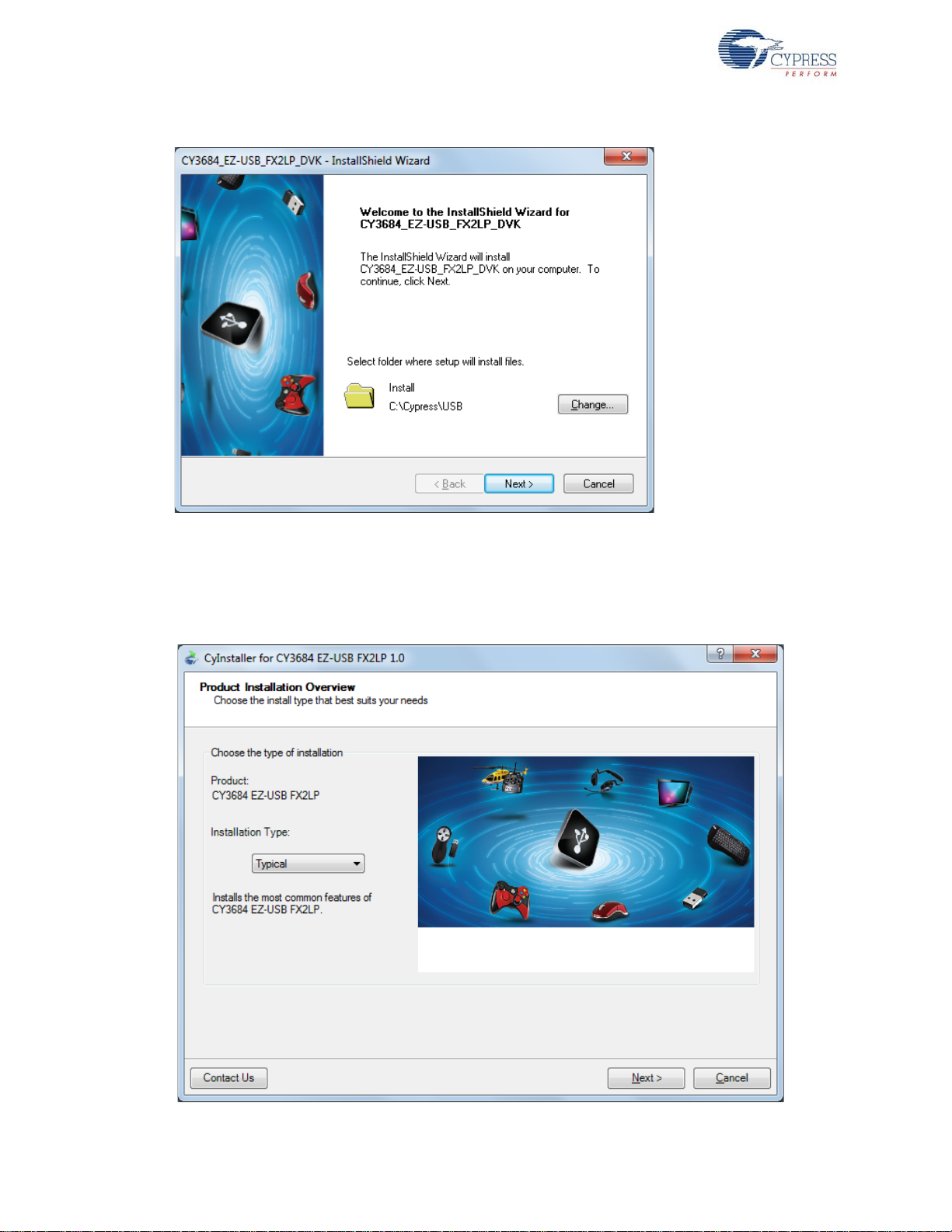
3. The InstallShield Wizard screen appears. The default location for setup is shown on the
InstallShield Wizard screen. You can change the location for setup using Change, as shown in
Figure 2-2. Click Next to launch the kit installer.
EZ-USB Development Kit User Guide, Doc. # 001-66390 Rev. *D 9
Page 10
Getting Started
Figure 2-2. InstallShield Wizard
4. On the Product Installation Overview screen, select the installation type that best suits your
requirement. The drop-down menu has three options - Typical, Complete, and Custom, as
shown in Figure 2-3. In the current installer, all three installation types result in the same set of
software getting installed. Select the default typical installation and click Next.
Figure 2-3. Installation Type Options
10 EZ-USB Development Kit User Guide, Doc. # 001-66390 Rev. *D
Page 11
Getting Started
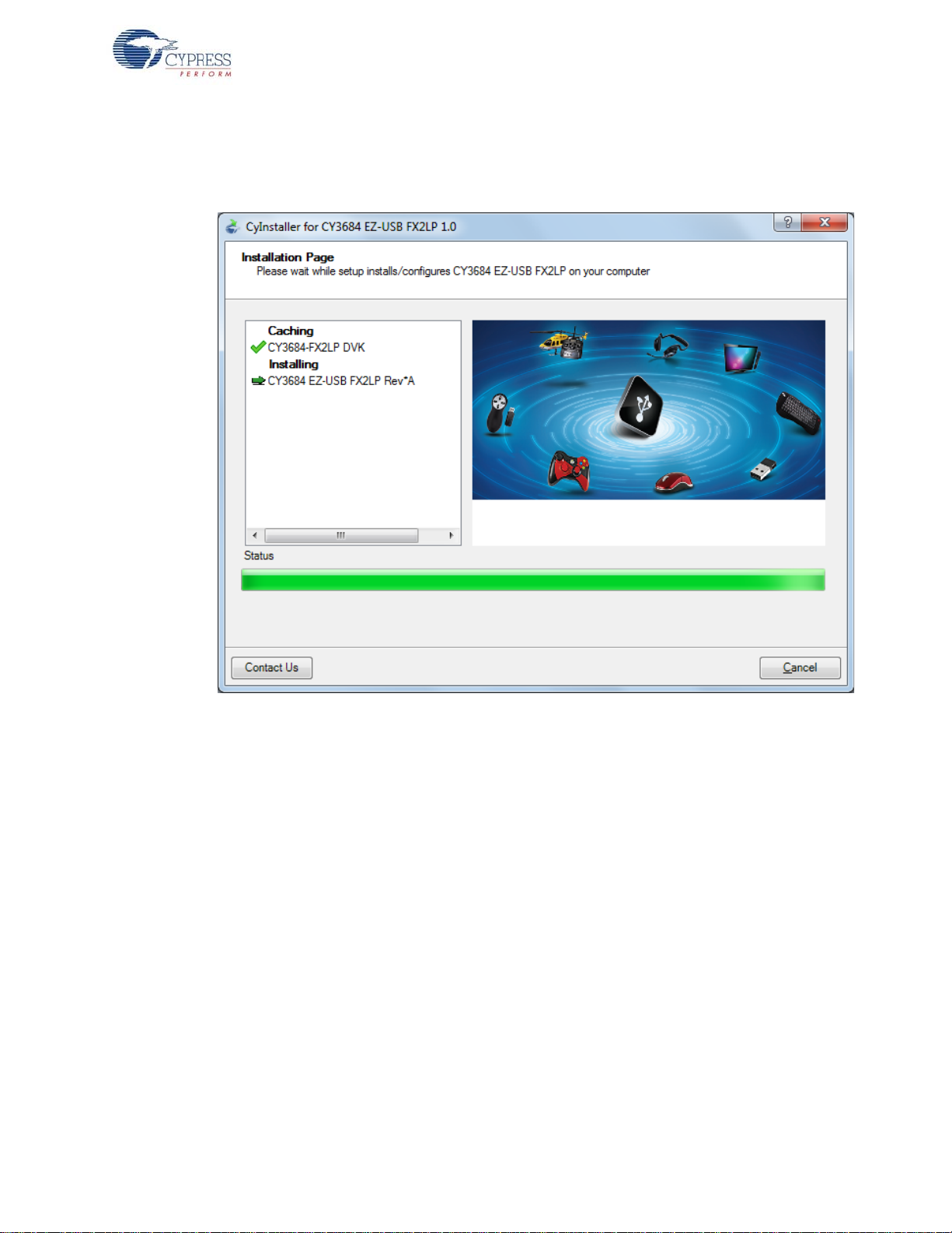
5. When the installation begins, all packages are listed on the Installation page. A green check mark
appears adjacent to every package that is downloaded and installed, as shown in Figure 2-4.
Wait until all the packages are downloaded and installed successfully.
Figure 2-4. Installation Page
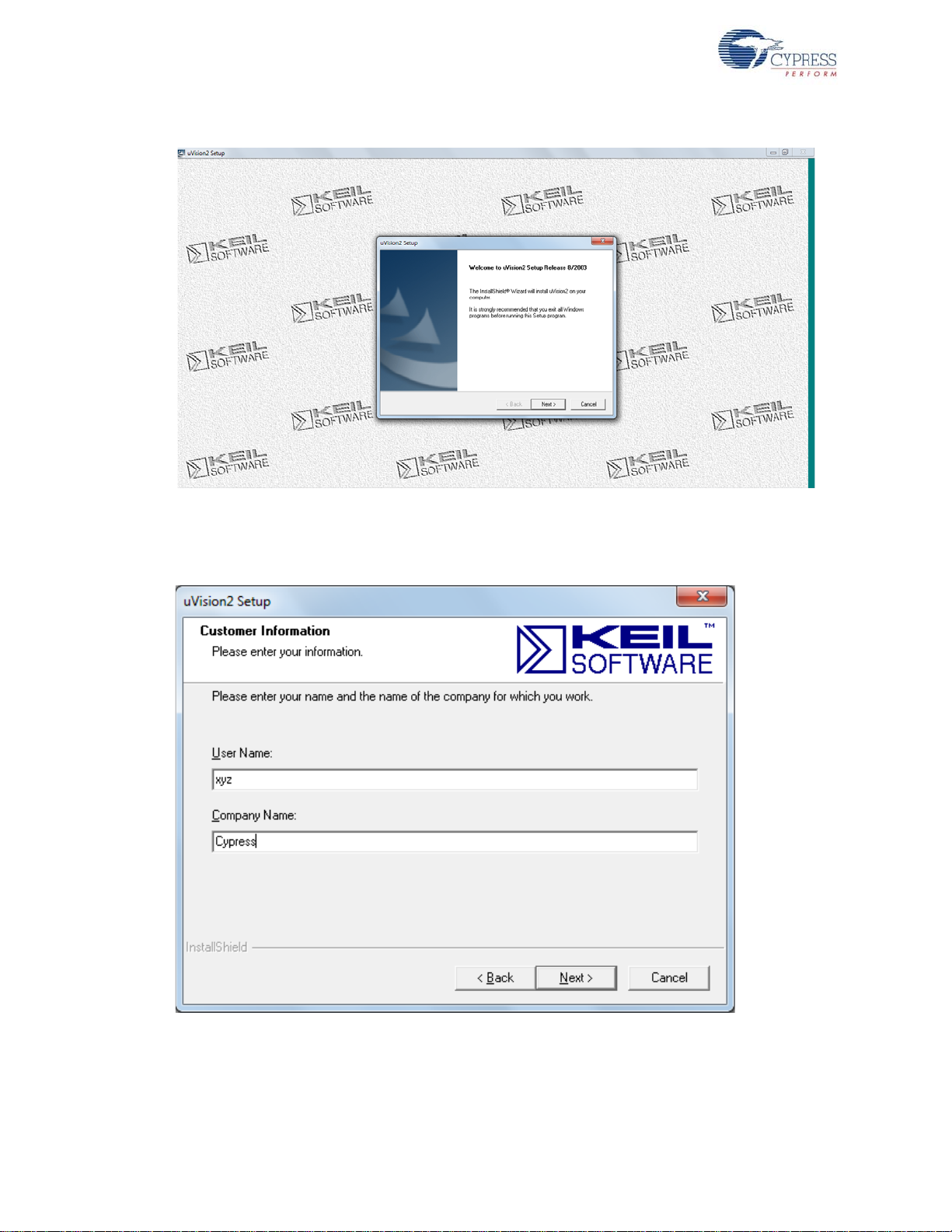
6. The Keil uVision2 trial version IDE triggers at this stage. If the software is already installed in the
PC, then the installer will not trigger the installation. If the PC does not contain the software, then
the Keil welcome screen appears, as shown in Figure 2-5. Click Next.
EZ-USB Development Kit User Guide, Doc. # 001-66390 Rev. *D 11
Page 12
Getting Started
Figure 2-5. Keil Welcome Screen
7. Enter the user name and company name credentials, as shown in Figure 2-6, to proceed with th e
installation.
Figure 2-6. Keil User Information lnput Window
8. The Keil software proceeds with the inst allation and copies the necessary packages at the default
directory C:\Keil. After completion, click on Finish, as shown in Figure 2-7.
12 EZ-USB Development Kit User Guide, Doc. # 001-66390 Rev. *D
Page 13
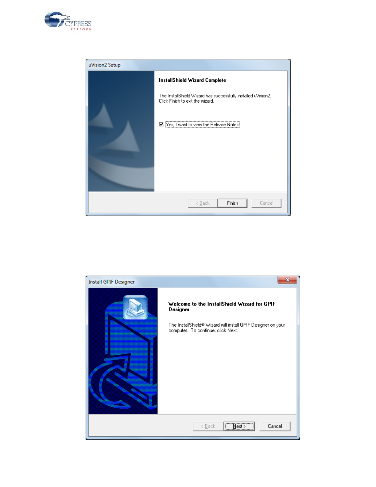
Figure 2-7. Keil User Information lnput Window
Getting Started
9. The GPIF designer software is triggered after Keil installation.This software is used to create
State machine waveforms to communicate between the EZ-USB device and devices such as
FPGA, image sensors, FIFO, and so on. If the software is already installed in the PC, then the
installer will not trigger the installation. If the PC does not contain the software, then the GPIF
Designer welcome screen appears, as shown in Figure 2-8. Click Next.
Figure 2-8. GPIF Designer Welcome Window
EZ-USB Development Kit User Guide, Doc. # 001-66390 Rev. *D 13
Page 14

Getting Started
10. Click Next in the subsequent windows and the Finish window appears, as shown in Figure 2-9.
Figure 2-9. GPIF Designer Welcome Window
11. The SuiteUSB 3.4.7 package install shield is triggered after the GPIF designer software installation. If the software is already installed in the PC, then the installer will not trigger the installation.
If the PC does not contain the software, then the SuiteUSB welcome screen app ears , as sho wn
in Figure 2-10. Click Next and accept the Cypress Software license agreement, as shown in
Figure 2-11.
Figure 2-10. SuiteUSB Welcome Window
14 EZ-USB Development Kit User Guide, Doc. # 001-66390 Rev. *D
Page 15
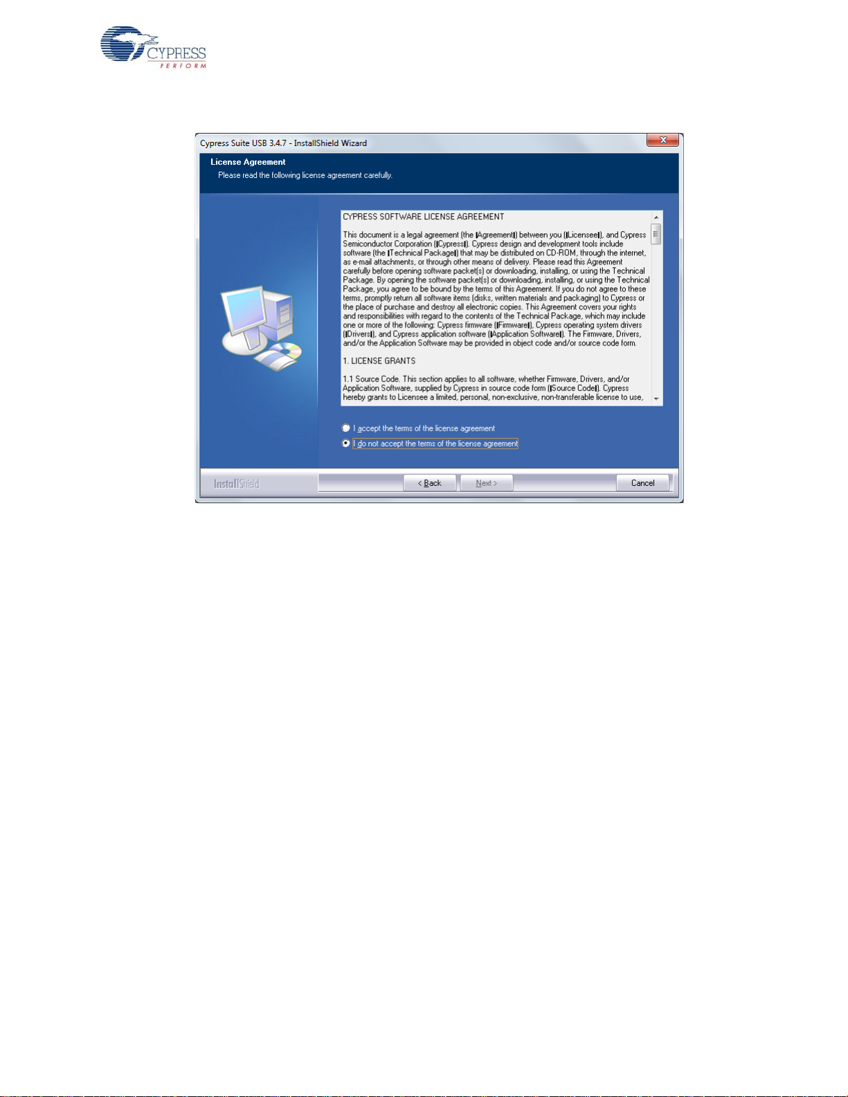
Figure 2-11. SuiteUSB License Agreement Window
Getting Started
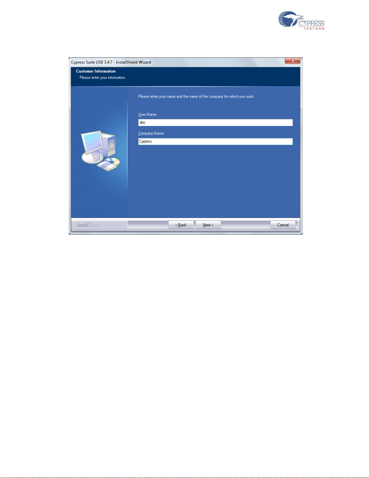
12.Enter the user credentials in the SuiteUSB window, as shown in Figure 2-12. Click Next. The
default directory of the SuiteUSB is C:\Cypress\Cypress Suite USB 3.4.7. The default
directory can be changed at this stage. Click Next after selecting the directory. Click the Install
button in the subsequent window. The SuiteUSB package installation progress is shown in the
next window. Finally the SuiteUSB Finish window appears. Click Finish button to complete the
installation process of SuiteUSB.
EZ-USB Development Kit User Guide, Doc. # 001-66390 Rev. *D 15
Page 16
Getting Started
Figure 2-12. SuiteUSB User Login Window
13.The CY3684 EZ-USB FX2LP development Kit Finish window appears after installing the kit content, Keil software, GPIF Designer, and the SuiteUSB 3.4.7 package.
16 EZ-USB Development Kit User Guide, Doc. # 001-66390 Rev. *D
Page 17
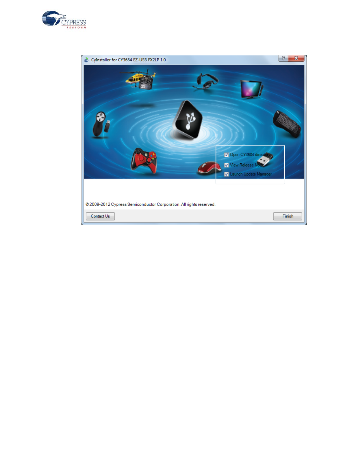
Figure 2-13. CY3684 Finish Window
Getting Started
Note The procedure to install the CY3674 installer is similar to CY3684.
2.2 Install Hardware
No hardware installation is required for this kit.
EZ-USB Development Kit User Guide, Doc. # 001-66390 Rev. *D 17
Page 18

Getting Started
18 EZ-USB Development Kit User Guide, Doc. # 001-66390 Rev. *D
Page 19

3. Advanced Development Board
3.1 Introduction
The EZ-USB Advanced Development Board provides a compact evaluation and design vehicle for
the EZ-USB family. The board provides expansion and interface signals on six 20-pin headers. A
mating prototype board allows quick construction and testing of USB designs. All ICs on the board
operate at 3.3 V. The board can be powered from the USB connector.
The EZ-USB Advanced Development Board is supplied as part of the Cypress EZ-USB DVK, which
includes an evaluation version of Cypress-customized software development tools from Keil
Software Inc. The Keil 8051 assembler, C compiler, and debugger work with the development board
to provide a complete code development environment. An 8051 debu g monitor is typically loaded
into the development board expansion RAM to leave the internal RAM free for code development.
The evaluation version of the Keil tools that ships with the DVK has several restrictions that make it
inappropriate for real-world development. Most significantly, it limits the compiled object size to 4 KB.
The full retail version allows a code of any size.
3.2 Schematic Summary
Read this description while referring to the EZ-USB FX2LP development board schematic and the
FX2LP development board assembly drawing. Both drawings are located in the Schematic on
page 114 and are available in PDF format in the DVK hardware directory. With the exception of the
EZ-USB chip, the development boards in the FX2LP and FX1 DVKs are identica l an d are r efer red to
generically as the EZ-USB development board in the following sections.
U1 is either EZ-USB FX2LP (CY7C68013A-128AC) or FX1 (CY7C64713-128AC). This is the fullfunction EZ-USB chip, which brings out the 8051 address and data buses for external memory
expansion. U2, a reprogrammable GAL, provides RAM enable signals for four jumper-selectable
memory maps. U3 is a 128-KB RAM, used for external 8051 memory expansion. Only 64 KB of this
memory is addressed by the 8051; the A16 pin is connected to a pull-up resistor that can be
attached to a GAL output to provide bank switching options.
U4 is a 3.3-V, 500-milliamp voltage regulator. U5 and U6 are socketed EEPROMS, used for EZ-USB
initialization and 8051 general-purpose access. U7 converts the 3.3-V 8051 serial port signals to
bipolar RS-232 levels. U8 and U10 are Philips PCF8574 I/O expanders, which attach to the EZ-USB
2
I
C bus and provide eight GPIO pins. U10 reads the four push-button switches, S2–S5, and U8
drives the 7-segment readout U9.
Six 20-pin headers, P1-P6, provide interface signals to the plug-in prototyping board supplied in this
kit. They also serve as connection points for HP (Agilent) logic analyzer pods. P8 contains a subset
of signals from P1–P6 on a connector that is pinned out for connection to a ‘straight-through’ ATA
cable.
Two slide switches, SW1 and SW2, control the connection and selection of the two socketed
EEPROMS at U5 and U6.
EZ-USB Development Kit User Guide, Doc. # 001-66390 Rev. *D 19
Page 20

Advanced Development Board
3.3 Jumpers
Table 3-1. EZ-USB Development Board Jumpers
Jumper Function Default Notes
JP1, JP10
JP2
JP3
JP5 3.3 V power IN (1-2)
JP6, JP7 Memory map selection OUT (1-2)
JP8 Wakeup2 pin OUT (1-2)
JP9
Connects 3.3 V power to
the EZ-USB chip.
Powers the on-board 3.3 V
regulator from USB Vbus
pin
Connects four GAL pins to
LEDS D2, D3, D4, D5
2
C bus test points
I
IN (1-2)
IN (1-2)
IN (1-2) (3-4)
(5-6) (7-8)
N/A
To operate the board in self-powered mode, remove
JP2 and supply 4 V to 5 V to JP2-1, and GND to a
ground pin (TP1 is a convenient GND point).
U2, the on-board GAL, contains code to use the four
LEDs as software indicators that can b e set . To use
the GAL pins for something else, which requires reprogramming the GAL or to wire the general purpose
indicators D2-D5 to other parts of the board, first
remove the appropriate shorting plug(s).
Supplies 3.3-V power to the board. It can be removed
and replaced with ammeter probes in series to measure board current.
These jumpers select one of the four memory maps
for U3, the external 128 KB RAM. See Memory Maps
on page 26 for details.
Inserting a shorting plug into JP8 connects an onboard RC network (R42,C43) to the secondary
remote wakeup pin WU2. This R-C network can be
used to test the periodic remote wakeup firmware
when this dual-purpose pin (it defaults to PA3) is programmed as WU2.
2
C bus SCL and SDA lines can be monitored or
The I
externally connected using JP9.
3.4 EEPROM Select and Enable Switches SW1 and SW2
SW1 selects between two socketed EEPROMs, one strapped to address 000 (U6), and the other
strapped to address 001(U5).
SW2 enables or disables the EEPROM selected by SW1.
The EZ-USB chip has various startup modes, which depend on the existence of an EEPROM
connected to its SCL and SDA lines. Switches SW1 and SW2 allow the EEPROMs to be
disconnected from FX1/FX2LP, or to be connected using one of the two EEPROMs installed in
sockets U5 and U6.
The EZ-USB chip contains two I
boot load controller operates when EZ-USB comes out of reset, and the 8051 controller operates
under firmware control when the 8051 is running, allowing the 8051 to access general-purpose I
devices connected to the SCL and SDA lines. The following section deals with the roles of SW1 and
SW2 in accommodating the various boot load mechanisms.
The EZ-USB bootloader accommodates two EEPROM types, in “Small” and “Large” versions, as
shown in Table 3-2.
20 EZ-USB Development Kit User Guide, Doc. # 001-66390 Rev. *D
2
C controllers, a “boot load” controller and an 8051 controller. The
2
C
Page 21

Advanced Development Board
Table 3-2. Typical EZ-USB external EEPROMS
EEPROM Type Size A2A1A0 Typical P/N
Small 16×8 000 24LC00
128×8 000 24LC01
256×8 000 24LC02
Large 8K×8 001 24LC64/5
Small EEPROMs are typically used to supply custom VID and PID information, allowing the EZ-USB
to enumerate with a driver associated with your EZ-USB design.
Large EEPROMs are typically used to boot-load code into the internal EZ-USB RAM, and then start
up the 8051 to execute this internal code, which performs the enumeration.
The EZ-USB loader determines the EEPROM size by first initiating an I
2
C transfer to address
1010000 (1010 is the EEPROM-class address, and 000 is the sub-address). If the device supplies
2
an I
C acknowledge pulse, the EZ-USB loader writes a single EEPROM address byte to initialize the
internal EEPROM address pointer to zero.
If this transfer does not return an ACK pulse, the EZ-USB loader initiates a second I
time to address 10100001 (1010 = EEPROM, sub-address 001). If an ACK is returned by the I
2
C transfer, this
2
device, the EZ-USB loader writes two EEPROM address bytes to initialize the internal EEPROM
address pointer to 0.
C
If neither transfer returns an ACK pulse, the EZ-USB loader boots in the ‘generic’ mode.
Three EZ-USB startup sequences and the associated settings for SW1 and SW2, are as follows:
■ Generic: SW2 = No EEPROM, SW1 = either position
When no EEPROM is connected to SCL and SDA, the EZ-USB chip enumerates using its internal, “hard-wired” VID and PID values. This mode can be selected without removing any socketed
EEPROMs by switching SW2 to the ‘off’ (down) position. This electrically disconnects any
EEPROMs that occupy the EEPROM sockets U5 and U6. The “OFF” mode is useful to start up
EZ-USB in a manner (using internal VID/PID) that binds the development system board to the
Cypress debug tools, such as the Control Panel and Keil. When running, SW2 ca n be switched to
the ON position to allow 8051 access, for example, to reprogram the EEPROM.
■ C0 Load: SW2 = EEPROM, SW1 = SMALL
A “C0” load provides EZ-USB with external Ve ndor ID (VID), Product ID (PID), and Device ID
(DID) values, allowing it to enumerate with the EEPROM-supplied VID, PID, and DID. At poweron, if the EZ-USB chip detects an EEPROM with the hex value ‘C0’ as its first byte, it continues to
load seven additional EEPROM bytes, which correspond to the USB VID, PID, DID, and an EZUSB configuration byte. When EZ-USB enumerates, it uses these EEPROM values instead of
the hard-wired internal values.
Because only eight bytes of data are required, a ‘small’ EEPROM is generally used for this mode;
for example, the 16-byte 24LC00.
■ C2 Load: SW2 = EEPROM, SW1 = LARGE
A “C2” load provides a method to load the EZ-USB internal RAM with 8051 firmware before enumeration. This boot load mechanism allows EZ-USB to enumerate as a fully custom device,
because the 8051 code handles enumeration using VID/PID values embedded in the code.
At power-on, if the EZ-USB chip detects an EEPROM with the hex value ‘C2’ as its first byte, it
continues to load an EZ-USB configuration byte, followed by blocks of 8051 code. The last byte
loaded takes the 8051 out of reset. This mode usually requires a large EEPROM, such as the
8 KB 24LC64.
EZ-USB Development Kit User Guide, Doc. # 001-66390 Rev. *D 21
Page 22

Advanced Development Board
Note If an EEPROM is connected to the SCL and SDA lines, but does not contain 0xC0 or 0xC2 as
its first byte, the loader reverts to the ‘generic’ case. In other words, the bootloader operates as
though no EEPROM is connected. However, when the 8051 is running, it has full access to any con-
nected EEPROM because the 8051 I
3.5 Interface Connectors
Table 3-3. Logic Analyzer Pinout
Agilent 01650-63203 Pod Pins
CLK1 3 4 D15
D14 5 6 D13
D12 7 8 D11
D10 9 10 D9
D8 11 12 D7
D6 13 14 D5
D4 15 16 D3
D2 17 18 D1
D0 19 20 GND
2
C controller is completely independent of the boot load logic.
Six 20-pin headers, P1–P6, on the EZ-USB Development Board have pins assigned to be compatible with HP (Agilent) logic analyzers, as shown in Table 3-3.
These six headers serve three purposes:
■ They mate with the prototyping board supp lied in the EZ-USB DVK.
■ They allow direct connection of the HP (Agilent) logic analyzer pods (Agilent P/N 01650-63203).
■ They allow general-purpose probing by other logic analyzers or oscilloscopes.
Table 3-3 shows the logic analyzer pod pin designations. The EZ-USB signals on P1–P6 are
arranged to fulfill the following requirements:
■ High-speed EZ-USB strobe signals (PSEN, WR#, CLKOUT, IFCLK, and RD#) are connected to
pin 3 of each of the five connectors for P1–P6. Therefore, they are used as the logic analyzer
clock, CLK1.
■ CLK2 is not used. Instead, each connecto r brings 3.3-V power from the EZ-USB development
board up to the prototype board using pi n 2.
■ The signals are logically grouped. For example, the 8051 address bus is on P5 and the EZ-USB
FIFO data, which shares PORTB and PORTD pins, is on P1.
The 20-pin headers on the prototyping board can be stacked. Therefore, it is possible to build custom circuitry on the prototyping board, plug the board into the EZ-USB development board, and still
plug the logic analyzer pods to the six connectors P1–P6. Table 3-4 to Table 3-9 show the EZ- USB
pin designations for P1 through P6. The alternate pin names are listed in the last columns.
22 EZ-USB Development Kit User Guide, Doc. # 001-66390 Rev. *D
Page 23

Table 3-4. Pin Designation (P1)
Alternate Default P1 Default Alternate
NC 1 2 3.3V
PSEN# 3 4 PD7 FD[15]
FD[14]PD65 6PD5FD[13]
FD[12] PD4 7 8 PD3 FD[11]
FD[10] PD2 9 10 PD1 FD[9]
FD[8] PD0 11 12 PB7 FD[7]
FD[6] PB6 13 14 PB5 FD[5]
FD[4] PB4 15 16 PB3 FD[3]
FD[2] PB2 17 18 PB1 FD[1]
FD[0] PB0 19 20 GND
Table 3-5. Pin Designation (P2)
Alternate Default P2 Default Alternate
NC 1 2 3.3V
NC 3 4 RDY1 SLWR
SLRD RDY0 5 6 CTL5
CTL4 7 8 CTL3
FLAGC CTL2 9 10 CTL1 FLAGB
FLAGA CTL0 11 12 PA7 FLAGD
PKTEND PA6 13 14 PA5 FIFOADR1
FIFOADR0 PA4 15 16 PA3 WU2
SLOE PA2 17 18 PA1 INT1#
INT0# PA0 19 20 GND
Advanced Development Board
Table 3-6. Pin Designation (P3)
Alternate Default P3 Default Alternate
NC 1 2 3.3V
WR# 3 4 RDY5
RDY4 5 6 RDY3
RDY2 7 8 BKPT
RESET# 9 10 N.C.
N.C. 11 12 PC7 GPIFADR7
GPIFADR6 PC6 13 14 PC5 GPIFADR5
GPIFADR4 PC4 15 16 PC3 GPIFADR3
GPIFADR2 PC2 17 18 PC1 GPIFADR1
GPIFADR0 PC0 19 20 GND
EZ-USB Development Kit User Guide, Doc. # 001-66390 Rev. *D 23
Page 24

Advanced Development Board
Table 3-7. Pin Designation (P4)
Alternate Default P4 Default Alternate
CLKOUT 3 4 GND
Table 3-8. Pin Designation (P5)
Alternate Default P5 Default Alternate
NC 1 2 3.3 V
OE# 5 6 CS#
5V 7 8 5V
PLD2 9 10 PLD1
N.C. 11 12 D7
D6 13 14 D5
D4 15 16 D3
D2 17 18 D1
D0 19 20 GND
NC 1 2 3.3 V
IFCLK 3 4 A15
A14 5 6 A13
A12 7 8 A11
A10 9 10 A9
A8 11 12 A7
A6 13 14 A5
A4 15 16 A3
A2 17 18 A1
A0 19 20 GND
Table 3-9. Pin Designation (P6)
Alternate Default P6 Default Alternate
NC 1 2 3.3 V
RD# 3 4 INT5#
INT4 5 6 T2
T1 7 8 T0
WAKEUP# 9 10 SDA
SCL 11 12 PE7 GPIFADR8
T2EX PE6 13 14 PE5 INT6
RxD1OUT PE4 15 16 PE3 RxD0OUT
T2OUT PE2 17 18 PE1 T1OUT
T0OUT PE0 19 20 GND
24 EZ-USB Development Kit User Guide, Doc. # 001-66390 Rev. *D
Page 25

3.6 ATA Connector P8
Table 3-10 shows the pinout for P8, a 40-pin connector that interfaces with a standard ATA cable.
This is for ATA use only. SP1, 2, and 3 should be bridged with the solder t o connect the ap propr iate
pull-up and pull-down resistors required for ATA. An 80-pin cable is required for UDMA transfer
modes and recommended for all transfer modes.
Table 3-10. P8 (ATA)
RESET# PA7 1 2 GND GND
DD7 PB7 3 4 PD0 DD8
DD6 PB6 5 6 PD1 DD9
DD5 PB5 7 8 PD2 DD10
DD4 PB4 9 10 PD3 DD11
DD3 PB3 11 12 PD4 DD12
DD2 PB2 13 14 PD5 DD13
DD1 PB1 15 16 PD6 DD14
DD0 PB0 17 18 PD7 DD15
GND GND 19 20 N.C. KEYPIN
DMARQ RDY1 21 22 GND GND
DIOW# CTL0 23 24 GND GND
DIOR# CTL1 25 26 GND GND
IORDY RDY0 27 28 GND CSEL
DMACK# CTL2 29 30 GND GND
INTRQ PA0 31 32 N.C. RESERVED
DA1 PA2 33 34 N.C. PDIAG#
DA0 PA1 35 36 PA3 DA2
CS0#PA43738PA5CS1#
DASP# 10K Pull-up 39 40 GND GND
Advanced Development Board
3.7 U2 - 22v10 Gate Array Logic (GAL)
A standard 22v10 GAL provides a general-purpose “glue logic” on the board. It provides the AND
gate required to combine the PSEN and READ signals, adds memory map support, debug LEDs,
and provides three spare outputs for customer-defined functions.
EZ-USB Development Kit User Guide, Doc. # 001-66390 Rev. *D 25
Page 26
Advanced Development Board
3.8 Memory Maps
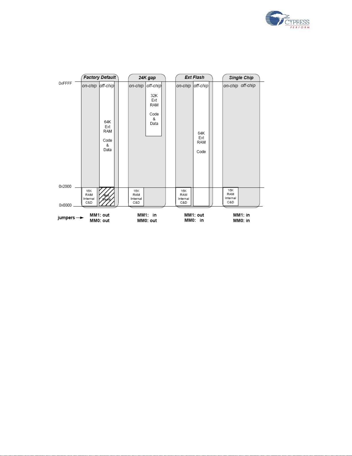
Figure 3-1. Four EZ-USB Development Board Memory Maps
Note The GAL sets EA=1 for the Ext Flash configuration only, enabling external code memory.
The factory default is to have both MM1 and MM0 jumpers removed. This setting should be used for
all development work using the Keil software tools.
■ The default configuration provides 16 KB of on-chip co de and data memory, plus 48 KB of exter-
nal RAM. The 8051 begins execution from internal RAM (the GAL sets EA=0). Although there is
an apparent overlap between the internal 16 KB and the botto m 16 KB of the external RAM,
EZ-USB disables RAM strobes for the bottom 16 KB, so there is no conflict. Th is EZ-U SB decoding allows using a standard 64-KB RAM without requiring external decoding to inhibit access to
the bottom 16 Kb.
■ The second column, “24K gap”, enable s the external RAM only for access to its upper 32 KB.
This configuration is useful for systems that add external devices that require memory-mapped
access. As with the default configuration, the 8051 begins execution from internal RAM (the GAL
sets EA=0).
■ The third column, “Ext Flash”, allows a flash memory (or other ROM) to be connected to the 8051
bus. This is the only configuration that starts 8051 execution from external memory (the GAL sets
EA to ‘1’). Because external memory occupies the bottom 16K, the internal EZ-USB RAM is
addressed only as data memory, instead of the combined program/data memory in the other
three configurations.
■ The fourth column, “Single Chip”, disables all external memory. This configuration is useful for
testing the final code to ensure that it does not use external resources present in the development environment.
26 EZ-USB Development Kit User Guide, Doc. # 001-66390 Rev. *D
Page 27

3.9 I2C Expanders
U8 and U10 are Philips PCF8574 I/O expanders. They connect to the I2C bus SCL and SDA pins,
and provide eight GPIO pins. U8 provides eight output bits, connected to the 7- segm ent r eadout U9.
U10 provides eight input bits: four connect to push buttons S2–S5 and four are uncommitted.
U8 connects to the 7-segment readout (U9) using the following bit assignments.
Figure 3-2. Bit Assignment
U8 has the group address 0100 and is strapped to the unit address 001. Therefore, to write a value
to the 7-segment readout, 8051 firmware sends a control byte of 01000010 (the least significant bit
(LSB0 indicates a write operation), followed by the da ta byte.
Advanced Development Board
U10 uses its I/O pins as inputs, connected to S2-S5 according to the followin g table.
Bit Switch
0S2
1S3
2S4
3S5
U9 has the group address 0100 and is strapp ed to unit address 000. Therefor e, to read the switch
values, the 8051 firmware sends a control byte of 01000001 (the LSB indicates a read operation),
and then reads the data byte.
3.10 Indicators – Power and Breakpoint
LED D1 is connected to the PCB 5-V power sup ply, which is normally supplied from the USB cable
(VBUS pin). Alternatively, JP2 can be removed and an external 5-V power can be applied to the JP2
pin 1. In either case, D1 indicates the presence of the 5-V power.
LED D6 is connected to the 3.3-V voltage regulator output.
LED D7 is connected to the EZ-USB breakpoint (BKPT) pin. When using the Keil software develop-
ment tools, this green LED indicates that the EZ-USB development board has enumerated and the
Keil monitor has loaded and started running.
EZ-USB Development Kit User Guide, Doc. # 001-66390 Rev. *D 27
Page 28
Advanced Development Board
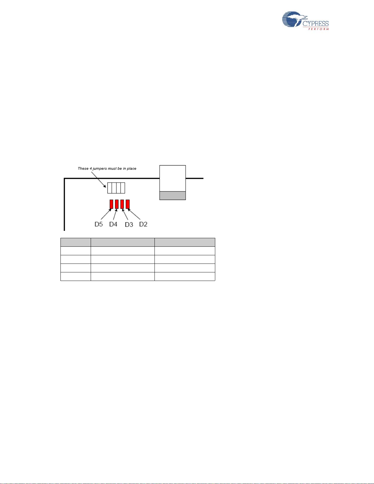
3.11 General-Purpose Indicators
A portion of the GAL (U2) decodes 8051 reads to cer t ain extern al memory a ddresses to tu rn the four
general-purpose indicators D2–D5 on and off. The following figure shows the positions of the four
indicator LEDs and a table of the external 8051 addresses, which are read to turn them on and off.
The four jumpers above the LEDS must be installed to use this feature. These jumpers connect the
LEDS to four GAL outputs.
Notes
■ The CLKOUT signal is used as a clock to latch the LED output signals from the GAL. If CLKOUT
is disabled, the LEDs will not update.
■ To use the LEDS for other purposes, such as wiring to other PC board signals for observation,
first remove the shorting plug to disconnect the LED from the GAL. The LED terminal is the bottom pin of the connector and the GAL I/O pin is the top pin.
Figure 3-3. Indicator LED Positions
Indicator Turn ON by Reading Turn OFF by Reading
D2 0x88-- 0x80-D3 0x98-- 0x90-D4 0xA8-- 0xA0-D5 0xB8-- 0xB0--
The low address byte is “don’t c are”. This means you can efficiently add software test points using
the following code:
D5ON: mov MPAGE,#B8h ; turn D5 on
movx a,@r0 ; dummy read
;
D5OFF: mov MPAGE,#B0h ; turn D5 off
movx a,@r0 ; dummy read
This code example uses the 8051 8-bit indirect addressing mode. The MPAGE register (SFR 0x92)
supplies the high address byte and r0 supplies the low address byte. Register r0 does not r equire initialization because the low address byte is “don’t care” for the LED decoding.
To turn the LEDs ON and OFF using the C code, declare the external memory locations, and then
read their values into dummy variables:
xdata volatile unsigned char D5ON _at_ 0xB800;
xdata volatile unsigned char D5OFF _at_ 0xB000;
unsigned char dum;
dum = D5ON; // turn D5 on
dum = D5OFF; // turn D5 off
Note Program execution a t these addresses do not activate the LEDs.
28 EZ-USB Development Kit User Guide, Doc. # 001-66390 Rev. *D
Page 29
4. Development Kit Contents
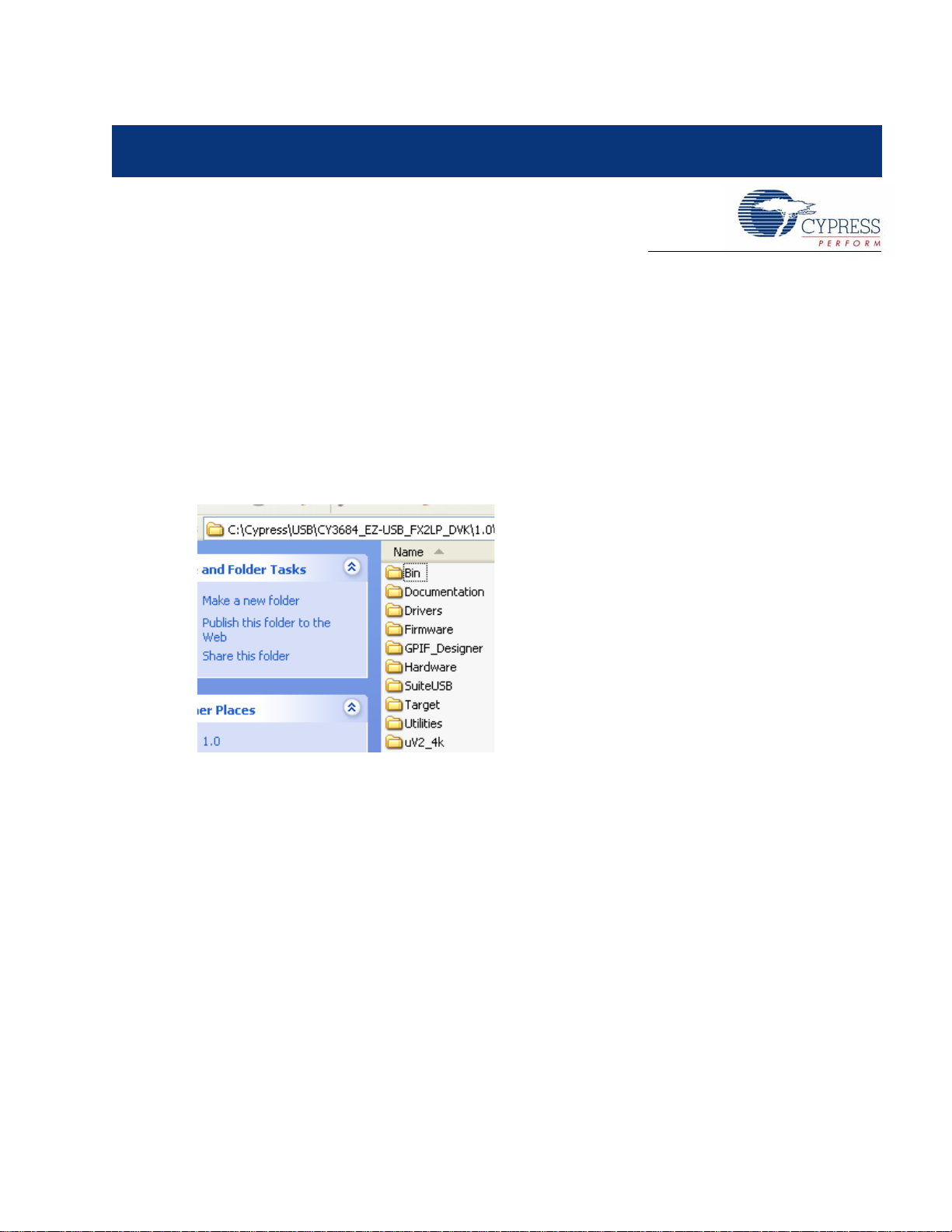
This section provides a detailed description of the structure and content of the EZ-USB DVK as it
exists on a user PC after installation. The following image shows the root-level tree after DVK installation. This assumes that all the DVK components are installed (the default installation type is ‘Typical’). Subsequent sections detail the contents of each sub-directory. The DVK installer installs
several files related to the development board in the Windows directory tree as shown in Figure 4-1.
The default directory for the CY3674 kit is C:\Cypress\USB\CY3674_EZ-USB_FX1_DVK\ an d for
the CY3684 kit, it is C:\Cypress\USB\CY3684_EZ-USB_FX2LP_DVK\. In further sections, the
default installation directory is referred to as <Installed_directory>, which refers to the
default directory of the respective EZ-USB kits.
Figure 4-1. CY3684 Development Kit Content Structure
4.1 Bin
This folder contains the following utilities
■ Cyscript.exe: This utility is used to generate script files for the equivalent firmware(.hex) files
■ Hex2bix.exe: This utility is used to convert a firmware image compatible to the RAM memory
(.hex) to an EEPROM image (.iic).
■ Setenv.bat: This is a batch file to set path variables for the Keil compiler and firmware examples.
Click on this batch file to set the environment variables necessary before compiling the firmware
examples of the kit.
EZ-USB Development Kit User Guide, Doc. # 001-66390 Rev. *D 29
Page 30

Development Kit Contents
4.2 Documentation
This directory contains documentation, which describes the EZ-USB DVK. The following table lists
the summary of the documents in the CY3674 and CY3684 EZ-USB development kits.
Table 4-1. Documents Summary for EZ-USB FX1 and FX2LP Development Kits
Kit Specific/
S.No
1 FX1(CY3674)
Common
Documents
Document Description
Migrating From AN21XX TO FX1 AN5040.pdf
™
Silicon Errata For EZ-USB
FamilY.pdf
EZ-USB FX1 Datasheet.pdf Datasheet for EZ-USB FX1 IC
FX1 Product
Application note to assist users to
migrate from Older Anchor IC to
EZ-USB FX1
Errata for EZ-USB FX1 IC
2 FX2LP(CY3684)
3 Common documents
4.3 Drivers
This directory contains Microsoft-certified, signed Cypress USB drivers for different Windows OS
platforms, such as Window 2000 (32-bit) and Windows XP, Vista, and 7 in 32- and 64-bit OS plat-
™
Migrating From EZ-USB FX2
USB FX2LP
EZ-USB® FX2LP Datasheet.pdf
Errata For The EZUSB-FX2LP.pdf Errata for EZ-USB FX2LP IC
Release Note EZ-USB FX1-EZ-USB
FX2LP
EZ-USB
ual.pdf
EZ-USB FX1-EZ-USB FX2LP
ment Kit Quick Start Guide.pdf
EZ-USB® Development Kit User
Guide.pdf
™
- AN4078_C.pdf
™
Development Kit.pdf
®
Technical Reference Man-
To EZ-
™
Develop-
Application note to assist users to
migrate from EZ-USB FX2 to EZUSB FX2LP
Datasheet for EZ-USB FX2LP IC
Release notes for both EZ-USB
FX1 and FX2LP development kits
Detailed manual which explains the
in detail about the entire IP blocks
and registers inside EZ-USB
device.
Quick start guide for EZ-USB FX1
and FX2LP devices.
This guide provides detailed
instructions on Kit software installation, Kit hardware, firmware examples and PC tools functionality.
30 EZ-USB Development Kit User Guide, Doc. # 001-66390 Rev. *D
Page 31

forms. Table 4-2 has the detailed list of drivers.
Table 4-2. USB Drivers in EZ-USB Development Kits
Development Kit Contents
S.No
1 cyusbfx1_fx2lp
2 CyMonfx1_fx2lp
3 CyLoad
Driver Package
Folder
4.4 Firmware
The EZ-USB development kit contains several firmware examples to validate different interfaces of
EZ-USB device. Following is the list of firmware examples.
Table 4-3. List of Firmware Example in EZ-USB Development Kits
Description
This directory contains the generic cyusb.sys driver information file,
cyusbfx1_fx2lp.inf, and the Microsoft caltalog file (cyusbfx1_fx2lp.cat) files
required to enumerate the EZ-USB devices.They .INF file contains default Fuse
ROM and firmware example VID/PIDs. For more details about this driver, go to
Chapter 6.
This directory contains the generic cyusb.sys driver information file,
CyMonfx1_fx2lp.inf, and the Microsoft caltalog (CyMonfx1_fx2lp.cat) files
required to debug the EZ-USB firmware examples. The .INF file contains the VID/
PID to automatically download the Keil debug monitor script file (mon.spt) to
assist you in step-by-step debugging of firmware examples. For more details
about this driver, go to Chapter 8.
This directory contains the generic cyusb.sys driver information file, CyLoad.inf,
and the Microsoft caltalog (CyLoad.cat) files required to debug the EZ-USB firmware examples. The .INF file contains VID/PID to automatically download the
firmware using the script file (CyLoad.spt). For more details about this driver, go
to Chapter 6.
S.No
1 hid_kb
2 Bulkloop
3 Bulkext
4 Bulksrc
5 dev_io
6 EP_Interrupts
7extr_intr
8Ibn
Firmware
Example
Description
Example firmware that emulates a HID-class keyboard using the buttons and a
7-segment display on the DVK board
Contains a bulk loopback test that exercises the EZ-USB bulk endpoints. It loops
back EP2OUT to EP6IN and EP4OUT to EP8IN.
Contains a bulk loopback test that exercises the EZ-USB bulk endpoints. The loopback is performed using the external auto pointer. Data is copied from the OUT
endpoint buffer to external RAM and then to the IN endpoint buffer. It loops back
EP2OUT to EP6IN and EP4OUT to EP8IN
Contains bulk endpoint endless source/sink firmware. It can be driven using the
CyConsole or CyBulk. EP2OUT always accepts a bulk OUT; EP4OUT always
accept a bulk OUT ; EP6IN always returns a 512-byte packet, 64 bytes at full-speed.
Based on the buffer availability in EP8IN, the most recent packet of EP4OUT is
written to EP8IN.
Contains the source files to build a simple development board I/O sample. This
software demonstrates how to use the buttons and LEDs on the EZ-USB development kit.
Bulk loopback firmware that demonstrates use of endpoint interrupts using EZ-USB
FX2LP.
Firmware that demonstrates external interrupt handling INT0, INT1, INT4, INT5,
and INT6.
Contains firmware to perform bulk loopback of EP2OUT to EP6IN and EP4OUT to
EP8IN using the IBN (In Bulk Nak) interrupt to initiate the transfer.
EZ-USB Development Kit User Guide, Doc. # 001-66390 Rev. *D 31
Page 32

Development Kit Contents
Table 4-3. List of Firmware Example in EZ-USB Development Kits
S.No
9 LEDCycle
10 Pingnak
11 iMemtest Memory test firmware example. Tests on-chip RAM.
12 vend_ax
Firmware
Example
4.5 GPIF_Designer
This directory contains the GPIF designer softwar e , which allows you to create State machine waveforms. These waveforms are useful to communicate with external devices, such as SRAM and
FPGA, using an EZ-USB GPIF interface.
4.6 Hardware
This directory contains the EZ-USB hardware schematic, PCB, Layout, gerber, and PCB BOM files.
Following are the files in this directory.
Table 4-4. List of Hardware Files in EZ-USB Development Kits
S.No Files Description
CY3684_Board_Layout.brd/
1
CY3674_Board_Layout.brd
CY3684_Board_Layout.pdf/
2
CY3674_Board_Layout.pdf
CY3684_Gerber.zip/
2
CY3674_Gerber.zip
CY3684_PCBA_BOM.xls/
3
CY3674_PCBA_BOM.xls
CY3684_Schematic.pdf/
4
CY3674_Schematic.pdf
CY3684_Schematic.dsn/
5
CY3674_Schematic.dsn
PDC-9022-A-Dimension.PDF,
PDC-9022-REVA.pdf, CY3681-
6
2_ASSEMBLY.pdf and PDC-9022A.zip
7 fx2lp.abl, fx2lp.jed
Description
Simple firmware example to demonstrate use of the general-purpose indicator
LEDs (D2, D3, D4, D5) on the development kit board.
Contains firmware to perform bulk loopback of EP2OUT to EP6IN and EP4OUT to
EP8IN using the PING NAK interrupt to initiate the transfer.
Contains the source files to build a vendor-specific command sample. This example
demonstrates how to implement different vendor commands.
This file is EZ-USB development board layout source file.This file
can be opened using the Allegro software
These files are non-editable board layout files of EZ-USB development board.
This .zip files contains PCB images of different layers of the EZUSB development board PCB.
This file contains components, such as resistors, capacitors, and
jumpers, used in designing the EZ-USB development board
This file is a non-editable version of the schematic source file
This file is an editable schematic source file. It can be opened
using Orcad software.
These files are part of the PROTO board daughter card,
designed to provide a sample prototype area for validating communication between the GPIF interface and the external device.
These files contain source logic for the GAL22LV10C device on
the EZ-USB development board
4.7 SuiteUSB
This folder contains the SuiteUSB 3.4.7 installer package and a sample Cypress Software License
agreement document. The software is installed as part of the EZ-USB Kit installer and the cont ents
are, by default, located at C:\Cypress\Cypress Suite USB 3.4.7.The package contains C++
32 EZ-USB Development Kit User Guide, Doc. # 001-66390 Rev. *D
Page 33

and C# .NET application tools to communicate with the EZ-USB device. In addition, it contains
Cypress generic USB drivers (3.4.7). These are unsigned drivers.
4.8 Target
This directory contains the EZ-USB register definition header files, Keil debug monitor, and so on.
Following are the list of files.
Table 4-5. List of Files in Target Directory
S.No Sub-directory File Description
1FW/Lp
2Monitor
3Inc
4Lib/Lp
Fw.c,periph.c
,dscr.a51,fw.uv2
mon-ext-sio0-c0.hex,
mon-ext-sio1-c0.hex,
mon-int-sio0-c0.hex,
mon-int-sio1-c0.hex,
mon-ext-sio0-c0.spt,
mon-ext-sio1-c0.spt,
mon-int-sio0-c0.spt
and
mon-int-sio1-c0.spt
fx2regs.h, lpregs.h
lpregs.inc,
fx2regs.inc
Fx2.h,
lp.h
syncdly.h,
fx2sdly.h
EZUSB.Lib USBJmpTb.OBJ
Development Kit Contents
This directory contains basic framework project source files
used to develop the firmware examples in the EZ-USB development kits
This directory contains Keil debug monitor .hex and script
files that reside in external SRAM memories or EZ-USB internal RAM. These files are used to debug firmware examples
through UART ports SIO-0 and SIO-1 at 38400 baud rate.
These files contain EZ-USB register definitions and basic
structure definitions.Also several delay routines of fixed duration (syncdly.h/fx2sdly.h)are defined to be used in frameworks code.
This folder mainly contains I2C read/Write routines
Library(EZUSB.lib) and Interrupt vector definitions for EZUSB device(USBJmpTb.OBJ)
4.9 Utilities
This directory contains the hex2bix utility source code in the VC++6 environment. The project code
can be used as a reference to invoke different command line options supported by this utility.
4.10 uV2_4k
This directory contains the Keil uVision2 Trial version IDE. The IDE has the limitation of compiling
the code limit of 4K. All the firmware examples included with the EZ-USB development kit can be
compiled using this IDE.
EZ-USB Development Kit User Guide, Doc. # 001-66390 Rev. *D 33
Page 34

Development Kit Contents
34 EZ-USB Development Kit User Guide, Doc. # 001-66390 Rev. *D
Page 35

5. EZ-USB Firmware Frameworks
The firmware frameworks simplify and accelerate USB peripheral development using the EZ-USB
chip. The frameworks implement the 8051 code for EZ-USB chip initialization, USB standard device
request handling, and USB suspend power management services. The user provides a USB
descriptor table and code to implement the peripheral function to complete a fully compliant USB
device. The frameworks provide function hooks and example code to help with this process. Th e
frameworks use the EZ-USB library to carry out common functions and for EZ-USB register definitions. Most of the firmware examples in the EZ-USB DVK are based on the frameworks.
5.1 Frameworks Overview
The frameworks implement the basic functionality required of a USB compliant peripher al device. By
linking a minimal descriptor table, it is possible to build a fully compliant Device Framework (USB
Specification, Chapter 9).
At startup, the frameworks initialize all its internal state variables. It then calls the user initialization
function TD_Init(). Upon return, the fra m eworks initialize the USB interface to the unconfig ur ed state
and enable interrupts. The firmware then re-enumerates and starts the co-operative task dispatcher.
The task dispatcher repeatedly performs the following tasks in the given order.
1. Calls the user function TD_Poll().
2. Determines if a standard device request is pending. If so, it parses the received command and
responds accordingly. The frameworks automatically handle the standard USB requests, but
allow the user to override the default behavior for all requests.
3. Determines if the USB core has reported a USB suspend event. If so, it calls the user function
TD_Suspend().
EZ-USB interrupts are handled by the frameworks. It provides hooks for user code notification of
USB events.
EZ-USB Development Kit User Guide, Doc. # 001-66390 Rev. *D 35
Page 36

EZ-USB Firmware Frameworks
Figure 5-1. Firmware Frameworks Flowchart
36 EZ-USB Development Kit User Guide, Doc. # 001-66390 Rev. *D
Page 37

5.2 Building FrameWorks
The framework is written using the Keil uVision2 Compiler. It is tested only with these tools. Because
the source uses several Keil C extensions, compatibility with other compilers is not guaranteed.
For your custom device firmware, you can either start with one of the firmware exampl es or star t with
the "clean" frameworks code. This code is located in the <Installed_directory>\<ver-
sion>\Target\fw directory. The sub-directory is chip dependent. For FX2LP and FX1, the firmware is located in the "LP" sub-directory. Before editing the firmware, create a new directory for your
project and copy the various frameworks source files into it.
After starting the Windows Command Prompt, run setenv.bat (located in the Bin directory) to set up
the build environment. This batch file assumes that you have installed the DVK and Keil tools in the
default directories.
The following table lists and describes the main files in the frameworks:
Table 5-1. Files in Firmware Frameworks
File Name Description
FW.C
PERIPH.C
DSCR.A51 Assembly file that contains your device's custom descriptors
FX2.H/LP.H
FX2REGS.H/
LPREGS.H
SYNCDL Y.H/
FX2SDLY.H
EZUSB.LIB EZ-USB Library object code. See EZ-USB Library on page 41 for more details
USBJMPTB.OBJ Object code that contains the ISR jump table for USB and GPIF interrupts
BUILD.BAT Batch file for compiling/linking the firmware using the Keil command line tools
FW.UV2 Keil uVision2 project file for compiling/linking the firmware
This is the main frameworks source file. It contains main(), the task dispatcher, and the
SETUP command handler. For most firmware projects, there is no need to modify this file
This source file contains initialization and task dispatch functions that are called from fw.c.
This is where you customize the frameworks for your specific device. This file also contains stub interrupt service routine (ISRs) functions for all of the USB (INT2) and GPIF
(INT4) interrupts
Head file containing common EZ-USB constants, macros, data types, and library function
prototypes
EZ-USB register declarations and bit mask constants
Contains the synchronization delay macro.
EZ-USB Firmware Frameworks
EZ-USB Development Kit User Guide, Doc. # 001-66390 Rev. *D 37
Page 38

EZ-USB Firmware Frameworks
5.3 Function Hooks
The frameworks provides function hooks to simplify the addition of user code. The functions are
divided into three categories: those called by the task dispatcher, the standard device request
parser , an d the USB interrupt hand ler. The following sections contain a complete list of functions and
their descriptions.
5.3.1 Task Dispatcher Functions
The following functions are called by the task dispatcher located in main().
5.3.1.1 TD_Init()
void TD_Init()
This function is called once during the initialization of the frameworks. It is called before ReNumeration and the Task Dispatcher starts. It is intended for the global state variable and device initialization.
5.3.1.2 TD_Poll()
void TD_Poll()
This function is called repeatedly during device operation. It should contain a state machine that
implements the user's peripheral function. High-priority tasks can be completed before returning
from this function. However, failure to return fro m this function prevent s frameworks from responding
to device requests and USB suspend events. If a large amount of processing time is required, it must
be split up to execute in multiple calls to TD_Poll().
5.3.1.3 TD_Suspend()
BOOL TD_Suspend()
This function is called before the frameworks enter suspend mode. This function contains code that
places the device in a low-power state and returns TRUE. However, the user code can prevent the
frameworks from entering suspend mode by returning FALSE.
5.3.1.4 TD_Resume()
void TD_Resume()
This function is called after the frameworks has resum ed the processor in response to an exter nal
resume event. At this point, the device resumes full-power operation.
5.3.2 Device Request Functions
These are helper functions that the device request handler (SetupCommand() in FW.C) calls. These
are mainly used to override or augment the default device request handler.
5.3.2.1 DR_GetDescriptor()
BOOL DR_GetDescriptor()
This function is called before the frameworks decode and implement the GetDescriptor device
request. The register array SETUPDAT contains the current eight byte setup command. It can be
parsed by the user's code to determine which Get Descriptor command is issued. If TRUE is
returned, the frameworks will parse and implement the command. If FALSE is returned, it will do
nothing.
38 EZ-USB Development Kit User Guide, Doc. # 001-66390 Rev. *D
Page 39

5.3.2.2 DR_GetInterface()
BOOL DR_GetInterface()
This function is called before the frameworks implement the Ge t In te rface device r equ est. T he reg i ster array SETUPDA T cont ains the current eight byte setup command. If TRUE is returned, the frameworks will implement the command. If FALSE is returned, it will do nothing.
5.3.2.3 DR_SetInterface()
BOOL DR_SetInterface()
This function is called before the frameworks implement the Set Interface device request. The register array, SETUPDAT, contains the current eight-byte setup command. It is the responsibility of this
routine to save the new interface setting and to do any necessary device configuration. If TRUE is
returned, the frameworks will implement the command. If FALSE is returned, it will do nothing.
5.3.2.4 DR_GetConfiguration()
BOOL DR_GetConfiguration()
This function is called before the frameworks implement the Get Configuration device request. The
register array, SETUPDAT, contains the current eight-byte setup command. If TRUE is returned, the
frameworks will implement the command. If FALSE is returned, it will do nothing.
EZ-USB Firmware Frameworks
5.3.2.5 DR_SetConfiguration()
BOOL DR_SetConfiguration()
This function is called before the frameworks implement the Set Configuration device request. The
register array, SETUPDAT, contains the current eight byte setup command. By default, the fram eworks parses the descriptor table to dete rmine the new configura tion interface and its endpoints. It
then configures the EZ-USB control registers to reflect these new endpoints. If the configuration is
set to 0 then the frameworks will invalidate all of the endpoints. If TRUE is returned, the frameworks
will implement the command. If FALSE is returned, it will do nothing.
5.3.2.6 DR_GetStatus()
BOOL DR_GetStatus()
This function is called before the frameworks implement the Get Status device request. The register
array, SETUPDAT, contains the current eight-byte setup command. If TRUE is returned, the frameworks will implement the command. If FALSE is returned, it will do nothing.
5.3.2.7 DR_ClearFeature()
BOOL DR_ClearFeature()
This function is called before the frameworks implement the Clear Feature device request. The register array, SETUPDAT, contains the current eight-byte setup command. If TRUE is returned, the
frameworks will implement the command. If FALSE is returned, it will do nothing.
5.3.2.8 DR_SetFeature()
BOOL DR_SetFeature()
This function is called before the frameworks implement the Set Feature device request. The register array, SETUPDAT, contains the current eight-byte setup command. If TRUE is returned, the
frameworks will implement the command. If FALSE is returned, it will do nothing.
EZ-USB Development Kit User Guide, Doc. # 001-66390 Rev. *D 39
Page 40

EZ-USB Firmware Frameworks
5.3.2.9 DR_VendorCmnd()
void DR_VendorCmnd()
This function is called when the frameworks determine a vendor specific co mmand has been issue d.
The register array, SETUPDAT, contains the current eight-byte setup command. This function has no
return value. The frameworks does not implement any vendor-specific co mmands. However, the EZUSB serial interface engine (SIE) uses vendor-specific command, 0xA0, to implement software
uploads and downloads. Therefore, command 0xA0 will not be passed to the user's code.
5.3.3 ISR Functions
There are over 40 different USB and GPIF auto-vectored interrupts available. PERIPH.C contains
stub ISR functions for all of these interrupts. This section documents the ISRs that require special
handling by device firmware. For more information, refer to the Interrupts chapter in the EZ-USB
Technical Reference Manual.
5.3.3.1 ISR_Sudav()
void ISR_Sudav(void) interrupt 0
This function is called on receiving the Setup Data Available interrupt. This function needs to set
GotSUD to TRUE so that the device request handler can process the SETUP command.
5.3.3.2 ISR_Sof()
void ISR_Sof(void) interrupt 0
This function is called on receiving the St art of Frame in terrupt. It get s called every 1 ms at full-speed
and every 125 uS at high-speed. The only action for this interrupt in the default frameworks code is
to clear the interrupt.
5.3.3.3 ISR_Ures()
void ISR_Ures(void) interrupt 0
This function is called on receiving the USB Reset interrupt. In your custom code, place any housekeeping that must be done in respon se to a USB bus reset in this rout ine. The default frameworks
code updates the configuration descriptor pointers in response to this interrupt. When a USB Reset
occurs, the device is always operating in full-speed (until high-speed chirp completes). Therefore, it
must return its full-speed configuration descriptor in response to a get configuration descriptor
request and must return its high-speed configuration descriptor in response to a get other-speed
descriptor request.
5.3.3.4 ISR_Susp()
void ISR_Susp(void) interrupt 0
This function is called on receiving the USB Suspend interrupt. The default frameworks code sets
the global variable Sleep to TRUE in this routine . This is required for the Task Dispatcher to detect
and handle the suspend event.
5.3.3.5 ISR_Highspeed()
void ISR_Highspeed(void) interrupt 0
This function is called on receiving the USB HISPEED interrupt. In your custom code, place any
housekeeping that must be done in response to a transition to high-speed mode in this routine.
The default frameworks code updates the configuration descriptor pointers in response to this interrupt. When the device switches to high-speed mode, it must return its high-speed configuration
40 EZ-USB Development Kit User Guide, Doc. # 001-66390 Rev. *D
Page 41

descriptor in response to a get configuration descriptor request and must return its full-speed configuration descriptor in response to a get other-speed descriptor request.
5.4 EZ-USB Library
The EZ-USB library is an 8051 .LIB file that implements functions th at are common to many fir mware
projects. These functions need not be modified an d are, therefor e, provided in library form. However,
the kit includes the source code for the library in the event that you need to modify a fu nction or if you
just want to know how something is done.
In addition to providing common functions, the library also creates register definitions for all EZ-USB
registers. The source code and the compiled .LIB file are located in the
<Installed_directory>\<Version>\Target\Lib\lp directory.
5.4.1 Building the Library
Only the full retail version of the Keil tools can build library files. The evaluation version will not build
this library.
After starting the Windows Command Prompt, run setenv.bat (located in the
<Installed_directory>\<Version>\Bin directory) to set up the build environment. This
batch file assumes that you have installed the DVK and Keil too ls in the default direct ories. To build
the library, run the build.bat file from the command prompt.
EZ-USB Firmware Frameworks
Build.bat also assembles the usbjmptb.a51 file to create usbjmptb.obj. This file contains the jump
table for the USB (INT2) and GPIF (INT4) auto-vectored interrupts. See the EZ-USB Technical Reference Manual (TRM) in the kit documentation for more information on auto-vector interrupts.
5.4.2 Library Functions
5.4.2.1 EZUSB_Delay()
void EZUSB_Delay(WORD ms)
This function performs a busy wait for a given number of milliseconds. The parameter ms determines the length of the busy wait. Upon completion of the delay the function returns.
5.4.2.2 EZUSB_Discon()
void EZUSB_Discon(BOOL renum)
This function performs a USB disconnect/reconnect. It disconnects the device, delays for 1500 ms,
clears any pending USB interrupts (INT2), reconnects, and then returns. The parameter renum
determines if the EZ-USB renumerate bit is set in the USB control register. If renum is TRUE, the
renumerate bit is set and following a return from this function, the 8051 will be responsible for handling all USB device requests on endpoint 0. If renum is FALSE, the renumerate bit is not modified. If
the renumerate bit is clear, then the EZ-USB serial interface engine handles most of the USB device
requests on endpoint 0.
5.4.2.3 EZUSB_GetStringDscr()
STRINGDSCR xdata * EZUSB_GetStringDscr(BYTE StrIdx)
This function returns a pointer to instance StrIdx of a string descriptor in the descriptor table. The
instance is determined by the StrIdx parameter. If the descriptor table does not contain the given
number of instances, then the function returns a NULL pointer.
EZ-USB Development Kit User Guide, Doc. # 001-66390 Rev. *D 41
Page 42

EZ-USB Firmware Frameworks
5.4.2.4 EZUSB_Susp()
void EZUSB_Susp(void)
This function suspends the processor in response to a USB suspend event. This function will not
return until the suspend is cleared by a USB bus resu me or a wake-up event on the EZUSB wa ke-up
pin. If a suspend event is not pending, this function will return immediately.
5.4.2.5 EZUSB_Resume()
void EZUSB_Resume(void)
This function generates the K-state on the USB bus required for a USB device remote wake-up. This
function should be called following a USB suspend. It automatically determines if the wake-up is
result of a USB resume or a remote wake-up and generates the K-state accordingly.
5.4.2.6 I2C Routines
void EZUSB_InitI2C(void);
BOOL EZUSB_WriteI2C_(BYTE addr, BYTE length, BYTE xdata *dat);
BOOL EZUSB_ReadI2C_(BYTE addr, BYTE length, BYTE xdata *dat);
BOOL EZUSB_WriteI2C(BYTE addr, BYTE length, BYTE xdata *dat);
BOOL EZUSB_ReadI2C(BYTE addr, BYTE length, BYTE xdata *dat);
void EZUSB_WaitForEEPROMWrite(BYTE addr);
These functions automate access to I
buttons on the DVK board. See the vend_ax and dev_io firmware examples for details on using
these functions.
2
C devices (such as the EEPROM), 7-segment display and
42 EZ-USB Development Kit User Guide, Doc. # 001-66390 Rev. *D
Page 43

6. Cypress USB Drivers for EZ-USB Kits
This chapter describes the Cypress USB drivers provided along with the kits. The USB-signed driver
package consists of several files to test different features of the EZ-USB (FX1/FX2LP) kits. It also
includes the SuiteUSB installer, which supports a collection of USB Host application tools designed
in C++ and C# .NET framework. These tools are useful to communicate with any Cypress USB 2.0
device.
6.1 Cypress USB Signed Driver Package for EZ-USB Devices
The EZ-USB (FX1/FX2LP) kits contain Microsoft-certified signed driver packages for different purposes. Following is the snapshot of the Drivers directory of the EZ-USB kit s.
Figure 6-1. Driver Packages in EZ-USB Kits
All these drivers support Windows 2000 (32-bit) and Windows XP, Vista, and 7 in both 32-bit as well
as 64-bit configurations. The following figure summarizes the list of folders specific to each OS.
Figure 6-2. Driver Sub-directory Summary
These folders contain signed driver files for relevant Windows OS platforms. Figure 6-3 shows the
snapshot of one of the signed driver package directories.
EZ-USB Development Kit User Guide, Doc. # 001-66390 Rev. *D 43
Page 44

Cypress USB Drivers for EZ-USB Kits
Figure 6-3. Sample Signed Driver Package
The basic set of files in a signed package is as follows:
■ Cyxxx.cat - These are Windows catalog files, which contain digital signature. This file indicates
that this driver-cyusb.sys passed the Microsoft driver certification process (WHQL).
■ Cyusb.sys - This is the Cypress-provided generic USB driver for all USB 2.0 products.The driver
version 3.4.5 is used in the driver certification process
■ Cyxx.INF - This file contains information about the .cat file and .sys file entries. The correspond-
ing destination directories for driver files or scripts are also defined to allow copying of these files
to Windows system folders. The INF file automates the process of driver loading and registering
the entry in the device manager of Windows.
The .INF files provided in the package should not be modified. These are provided to enable testing different features of the EZ-USB device. If the .INF file is edited, the Microsoft digital signature is
no longer valid. In addition, the default VID/PID mentioned in these INF files should not be used for
any other purpose except for te sting the basic features of th e device. Attempt to bind the modified
.INF file along with the existing .cat and .sys file results in a Warning window. The signed driver
loading conditions are stringent in Windows Vist a and Windows 7 64-bit configura tions. To temporarily avoid driver loading problems with the edited .INF file , press F8 du ring the Windo ws machine reboot, and select “Disable Driver signature Enforcement”. The 64-bit OS will still provide warnings
but allow the edited INF file loading. This setting does not propagate to the next re-boot and mu st b e
performed again during next re-boot.
Note To completely avoid these warnings, users should remove all the instances of the default VID/
PID in the .INF file and replace these with their own VID/PID combination. The modified .INF along
with cyusb.sys need s to be re-sub mitted to Micro soft for driver certification. For more details on the
WHQL re-submission process for the modified Cypress USB driver package, refer to the application
note, “AN52970 - Windows Hardware Quality Labs (WHQL) Signing Procedure for Customer Modi-
fied Cypress USB Driver Files”. Depending on the functionality of each of these .INF packages, they
are classified into two major categories:
■ Drivers for firmware examples and default EZ-USB configuration
■ Drivers for firmware and Keil monitor automatic download using script files
6.2 Drivers for Firmware Examples and Default EZ-USB Configuration
The EZ-USB FX1 and FX2LP kit uses several VID/PID for tasks, such as default enumeration (Fuse
ROM), firmware example re-enumeration, and so on. In the list of signed driver packages,
cyusbfx1_fx2lp.inf contains all the VIDs and PIDs relevant for th ese tasks. Table 6-1 gives a sum-
mary of VIDs and PIDs used in this .INF file.
44 EZ-USB Development Kit User Guide, Doc. # 001-66390 Rev. *D
Page 45

Cypress USB Drivers for EZ-USB Kits
Table 6-1. List of VID/PID used in EZ-USB Kits
S.No VID/PID Functional Description
EZ-USB FX2LP Fuse ROM VID/PID.This is the initial VID/PID when
the board is powered, with the SW2-NO EEPROM setting as the
1 0x04B4/0x8613
2 0x04B4/0x6473 EZ-USB FX1 Fuse ROM VID/PID
3 0x04B4/0x1004
4 0x04B4/0x1003
default combination
MOBL-USB FX2LP18 Connect Mode. Uses LP18_dvk.iic as the
default image in EEPROM to enable the DPTR register and enumerate with this VID/PID
Firmware examples in the EZ-USB kits use this combination except
for the hid_kb example, which uses 0x04B4/1005.This example
requires the Windows HID-Class driver and does not require a
Cypress USB driver
This is used by the Cystream firmware example available in SuiteUSB 3.4.7 supplied along with this kit. Download CYStream.hex
from C:\Cypress\Cypress Suite USB 3.4.7\Firm-
ware\CyStreamer using Cyconsole or CyControlCenter utility
and test it using Streamer applications available in SuiteUSB.The
procedure to download a firmware .hex file is explained in Chapter-7
of this document.
6.2.1 Binding Cypress USB Driver to EZ-USB Development Board
The EZ-USB (FX1/FX2LP) development board supplied with the kit is used to bind the signed
Cypress USB driver. Following are the steps to bind the driver:
1. Disconnect the USB A-to-B cable between the J1 connector and the PC USB Host port, if connected previously.
2. Verify the following default jumper settings for the EZ-USB FX1 and FX2LP boards.
FX1: Short on JP1, JP2, JP3, JP5, JP6, JP7, JP8, and JP10.
FX2LP: Short on JP1, JP2, JP3, JP5, JP8, and JP10. Open JP6 and JP7.
The functionality of each of these jumpers is explained in Chapter 3.
3. Verify if SW2 is switched to the side, marked as NO EEPROM.
4. Re-connect the USB A-to-B cable between the J1 connector and the PC USB Host port.
5. The EZ-USB FX1 (0x04B4/0x6473) and FX2LP (0x04B4/8613) boards enumerate with the
default Fuse ROM VID/PID.
6. The Windows hardware wizard window pops up allowing you to update the corresponding driver
path, as shown in Figure 6-4.
EZ-USB Development Kit User Guide, Doc. # 001-66390 Rev. *D 45
Page 46

Cypress USB Drivers for EZ-USB Kits
Figure 6-4. Windows Hardware Wizard for Driver Update
7. Select Yes, This time only and click Next. Select Install from a specific location and click
Next.
8. In the subsequent window, select Don't search. I will choose driver to install and select Next.
In the list of Hardware devices, select Universal Serial Bus Controllers and click on Have Disk
button. A new Window pops up for locating the USB driver. Click the Browse button and point to
the following directories for the corresponding Windows PC Host operating system with respect
to <Installed_directory>\<Version>\Drivers\cyusbfx1_fx2lp
a. Windows2000: w2k\x86
b. Windows XP(32-bit): wxp\x86
c. Windows XP(64-bit): wxp\x64
9. The Hardware wizard Window options differ in Windows Vista and Windows 7 OS platforms. If
the hardware wizard window does not pop up, then type devmgmt.msc directly in the vacant box
in Windows Start. Locate the Unknown Device marked in yellow. Right-click on the Unknown
Device and verify in Details > Hardware ID if the VID/PID match the Fuse ROM VID/PID for the
FX1 and FX2LP devices. Then, right-click again on the Unknown Device and select Update
Driver Software. The Windows OS Hardware wizard window will now pop up. If the hardware
wizard window pops up automatically, then the entire process mentioned in this step can be
avoided.
10.Select Browse my computer for driver Software. In the next window, under Browse for the
driver software on your computer, click Browse and select the following directory p aths for
Windows Vista and 7 OS:
a. Windows-Vista(32-bit): wlh-vista\x86
b. Windows-Vista(64-bit): wlh-vista\x64
c. Windows-7(32-bit): wlh-win7\x86
d. Windows-7(64-bit): wlh-win7\x64
46 EZ-USB Development Kit User Guide, Doc. # 001-66390 Rev. *D
Page 47

Cypress USB Drivers for EZ-USB Kits
11.Open the device manager, as mentioned in step 9, and expand the list of USB controllers.
12.Observe the EZ-USB device in the list of USB device controllers. Following are the strings for the
default Fuse ROM VID/PID of EZ-USB devices.
a. EZ-USB FX1:“Cypress EZ-USB FX1 No EEPROM(3.4.5.000)”
b. EZ-USB FX2LP:“Cypress EZ-USB FX2LP No EEPROM(3.4.5.000)”
This completes the entire binding process for the EZ-USB device. The process is similar for any
USB device with its own proprietary drivers.
6.3 Drivers for Firmware and Keil Monitor Automatic Download using Script Files
The firmware examples provided with the EZ-USB kits can be manually downloaded using Cyconsole or CyControlcenter. If you need to automate the firmware downloading process, then script
files can be used. Whenever the EZ-USB board with the relevant VID/PID to the script file is
detected, then the Windows OS automatically downloads the actual firmware inside the script and
the EZ-USB device re-enumerates with new VID/PID defined in the firmware. Following are the relevant driver files provided under the \Drivers directory:
■ CyLoad: This directory contains CyLoad.spt, Cyload.cat, CyLoad.inf, and cyusb.sys.These are
basic files required to automate the process of fi rmware download u sing script files and .INF files.
For more details, refer to Firmware Download using CyLoad Driver Package on page 49.
■ CyMonfx1_fx2lp: This directory contains mon.spt cymon.cat, CyMonfx1_fx2lp.inf and
cyusb.sys. The script file mon.spt contain s the Keil debug monitor. The Keil debug monitor, after
downloading to EZ-USB RAM memory, enables the user to debug EZ-USB firmware examples
using step-by-step debugging using the UART port at 38400 baud rate. The method to debug
firmware examples using this driver package is explained in Debugging Using Keil Monitor Pro-
gram on page 97.
6.3.1 How to Generate and Play Script Files (.spt)
The script files are generated for a specific firmware. Select the Bulkloop firmware example to
experiment for this purpose. Choose Bulkloop.hex under <Installed_directory>\<ver-
sion>\Firmware\Bulkloop in the EZ-USB Kit contents. The script file can be generated using
three tools available with the EZ-USB kits.
6.3.1.1 Script File Generation using the Cyscript Tool
Open this tool located at <Installed_directory>\<Version>\Bin after installing the EZ-USB
kit contents. Click the Browse button, adjacent to the Input HEX file, and select the path where the
.hex file is located. Choose the directory and file nam e of your ch oice for the scr ipt file a nd click Cre-
ate Script File button.
EZ-USB Development Kit User Guide, Doc. # 001-66390 Rev. *D 47
Page 48

Cypress USB Drivers for EZ-USB Kits
Verify if the xx.spt file is located in the destination directory. This tool can only generate a script but
cannot play the script. Using Cyconsole or Controlcenter, the generated script file can be loaded
and played to download the firmware inside the script.
6.3.1.2 Script File Generation and Play using CyConsole
Open the Cyconsole tool located at C:\Cypress\Cypress Suite USB 3.4.7\CyConsole.
Click on C:\Cypress\Cypress Suite USB 3.4.7\CyConsole. Alternately, the tool can be
accessed at Windows Start > All Programs > Cypress > Cypress SuiteUSB 3.4.7. Follow these
steps to generate and play the script.
Figure 6-5. Script Generation and Download Option in Cyconsole
1.Connect a USB A-to-B cable between the Windows PC USB Host port and the EZ-USB FX1/
FX2LP board J1 connector. The board should have switch SW2 with the NO EEPROM option
selected.
2.The EZ-USB FX1/FX2LP enumerates with the default Fuse ROM VID/PID.
3.Select the Record Script button
4.In the options menu, select EZ-USB Interface. Select Download in the new pop-up window and
browse to Bulkloop.hex at <Installed_directory>\<Version>\Firmware\Bulkloop
48 EZ-USB Development Kit User Guide, Doc. # 001-66390 Rev. *D
Page 49

5.Observe the Bulkloop.hex file getting downloaded successfully to the EZ-USB RAM memory. After
firmware download, click the Stop recording button and save the .spt file generated in the local
directory of choice.
6.Select the Load script button and choose the xxx.spt file generated in step 5.
7.Click on Play script. The entire firmware gets downloaded and the EZ-USB FX1/FX2LP re-enumerates with VID/PID -0x04B4/0x1004 defined in the firmware.
8.Open the device manager by clicking on Windows Start > Ru n. Type devmgmt.msc in the Run
box. If cyusbfx1_fx2lp.inf was binded to EZ-USB FX1/FX2LP earlier, as mentioned in Binding
Cypress USB Driver to EZ-USB Development Board on page 45, then the EZ-USB device enumer-
ates as Cypress EZ-USB Example Device(3.4.5.000).
6.3.1.3 Script Generation and Play using CyControlCenter
Open this tool located at C:\Cypress\Cypress Suite USB 3.4.7\CyUSB.NET\examples\Control Center\bin\Release after installing the EZ-USB kit contents. Click on
C:\Cypress\Cypress Suite USB 3.4.7\CyConsole. Alternately, the tool can be accessed at
Windows Start > All Programs > Cypress >Cypress Suite USB 3.4.7 > CyConsole. Follow these
steps to generate and play the script.
Figure 6-6. CyControlCenter Script Button Options
Cypress USB Drivers for EZ-USB Kits
1. Connect a USB A-to-B cable between the Windows PC USB Host port and the EZ-USB FX1/
FX2LP board J1 connector. The board should have SW2 switched to the side, marked as NO
EEPROM.
2. The EZ-USB FX1/FX2LP enumerates with the default Fuse ROM VID/PID.
3. Click the Create Script button and select Bulkloop.hex at <Installed_directory>\<Ver-
sion>\Firmware\Bulkloop. Save the file as Bulkloop.spt to any local directory of choice.
4. Select the Load script button and choose the Bulkloop.spt file generated in step 3.
5. Click on Play script. The entire firmware gets downloaded and the EZ-USB FX1/FX2LP re-enu-
merates with VID/PID -0x04B4/0x1004 defined in the firmware.
6. Open the device manager by clicking on Windows Start > Run. Type devmgmt.msc in the Run
box. In the Windows Vista and 7 OS platforms, type devmgmt.msc directly in the vacant box
near Start button. If cyusbfx1_fx2lp.inf was binded to EZ-USB FX1/FX2LP previously as mentioned in section Binding Cypress USB Driver to EZ-USB Development Board chapter on
page 45 then EZ-USB device enumerates as Cypress EZ-USB Example Device(3.4.5.000).
6.3.2 Firmware Download using CyLoad Driver Package
In the previous section, the procedure to generate the script files and play the scripts were
described.The entire process of script-based firmware download can be automated using .INF files.
The CyLoad driver package contains several files to a ssist the user in au to-download of the firmware
using the script file. Following are the files for CyLoad driver package.
EZ-USB Development Kit User Guide, Doc. # 001-66390 Rev. *D 49
Page 50

Cypress USB Drivers for EZ-USB Kits
1. CyLoad.cat: These are Windows Catalog files which indicates that the USB driver cyusb.sys
passed Microsoft driver certification (WHQL) process.
2. Cyusb.sys: This is the cypress provided generic USB driver for all USB 2.0
products. The driver version 3.4.5 was used in the driver certification process
3. CyLoad.inf: This driver information file contains details about the CyLoad.spt,
CyLoad.cat and cyusb.sys driver file entries. The corresponding destination directories for driver
file and script file are also mentioned.The .INF file automates the process of firmware loading
using these files.
4. CyLoad.iic: Small EEPROM Image which contains VID/PID -0x04B4/0x0084
matching the VID/PID of Cyload.inf file. After downloading this file to EZ-USB development board
it re-enumerates with this VID/PID and script file is automatically triggered by Windows OS.
5. CyLoad.spt: The script file which automates firmware downloading to a EZ-USB
device.
Following is the snapshot of CyLoad.inf file content located at <Installed_directory>\<Ver-
sion>\Drivers\CyLoad for different Windows PC Host platforms
[Version]
Signature="$Windows NT$"
Class=USB
ClassGUID={36FC9E60-C465-11CF-8056-444553540000}
provider=%CYUSB_Provider%
CatalogFile=CyLoad.cat
DriverVer=01/19/2011,3.04.0005.000
[SourceDisksNames]
1=%Cyload_INSTALL%,,,
[SourceDisksFiles]
CyUsb.sys = 1
CyLoad.spt = 1
[DestinationDirs]
CyLoadFW.Files = 10, System32\CyLoad
CYUSB.Files.Ext = 10, System32\Drivers
[ControlFlags]
ExcludeFromSelect = *
[Manufacturer]
%CYUSB_Provider%=Device, NT, NTx86, NTamd64
;for all platforms
[Device]
;%VID_XXXX&PID_XXXX.DeviceDesc%=CyLoad, USB\VID_XXXX&PID_XXXX
%VID_04B4&PID_0084.DeviceDesc%=CyLoad, USB\VID_04B4&PID_0084
;for windows 2000 non intel platforms
[Device.NT]
;%VID_XXXX&PID_XXXX.DeviceDesc%=CyLoad, USB\VID_XXXX&PID_XXXX
%VID_04B4&PID_0084.DeviceDesc%=CyLoad, USB\VID_04B4&PID_0084
;for x86 platforms
50 EZ-USB Development Kit User Guide, Doc. # 001-66390 Rev. *D
Page 51

Cypress USB Drivers for EZ-USB Kits
[Device.NTx86]
;%VID_XXXX&PID_XXXX.DeviceDesc%=CyLoad, USB\VID_XXXX&PID_XXXX
%VID_04B4&PID_0084.DeviceDesc%=CyLoad, USB\VID_04B4&PID_0084
;for x64 platforms
[Device.NTamd64]
;%VID_XXXX&PID_XXXX.DeviceDesc%=CyLoad, USB\VID_XXXX&PID_XXXX
%VID_04B4&PID_0084.DeviceDesc%=CyLoad, USB\VID_04B4&PID_0084
……
[CyLoad]
CopyFiles=CyLoadFW.Files
AddReg=CyLoad.AddReg
[CyLoad.HW]
AddReg=CyLoad.AddReg.Guid
[CYLoad.Services]
Addservice = CyLoad, 2,CyLoad.AddService
[CyLoad.NT]
CopyFiles=CyLoadFW.Files
AddReg=CyLoad.AddReg
[CyLoad.NT.HW]
AddReg=CyLoad.AddReg.Guid
[CyLoad.NT.Services]
Addservice = CyLoad,2,CyLoad.AddService
......
[CyLoadFW.Files]
CyLoad.spt
[CyLoad.AddReg.Guid]
HKR,,DriverGUID,,%CyLoad.GUID%
HKR,DriverEXECSCRIPT,,%CyLoad.EXECSCRIPT%
[CYUSB]
CopyFiles=CYUSB.Files.Ext
AddReg=CyUsb.AddReg
[CYUSB.HW]
AddReg=CYUSB.AddReg.Guid
[CYUSB.Services]
Addservice = CYUSB, 2,CYUSB.AddService
[CYUSB.Files.Ext]
CYUSB.sys
[CYUSB.AddReg.Guid]
HKR,,DriverGUID,,%CYUSB.GUID%
EZ-USB Development Kit User Guide, Doc. # 001-66390 Rev. *D 51
Page 52

Cypress USB Drivers for EZ-USB Kits
;------------Modify these strings to match your device--------------------
-----------;
CyLoad_INSTALL = "Cypress USB Fwload Installation Disk(3.4.5.000)"
VID_04B4&PID_0084.DeviceDesc="Cypress EZ-USB Example Device Firmware Download(3.4.5.000)"
CyLoad.SvcDesc = "Cypress EZ-USB Fwload(3.4.5.000)"
The important sections in this .INF file are
■ [SourceDisksFiles] section contains the necessary source files to download the firmware -
cyusb.sys and CyLoad.spt
■ [DestinationDirs] refer to Windows system folder where the source files are copied-cyusb.sys
copied to C:\Windows\system32\Drivers and CyLoad.spt to C:\Win-
dows\system32\CyLoad. For a Windows PC with multiple OS on different partitions the relevant partition for active OS is used to copy the files.
■ The INF file is supported on different Windows OS platforms - 2000, XP, Vista and 7 using stan-
dard OS identifiers NT, NTx86 and NTamd64.
■ ‘CopyFiles=CyLoadFW.Files’ refers to another section CyLoadFW.files, which is in turn are
defined as:
❐ [CyLoadFW.Files]
❐ CyLoad.spt
The script file is the actual file defined by this section to be copied into the destination directory
defined in the [DestinationDirs] section.
■ The Cypress generic USB driver (ver 3.4.5) is also copied in a similar manner to Windows OS
System folders defined under [DestinationDirs] section.
■ The VID/PID-0x04B4/0x0084, which is part of the .INF file is linked to Cyload.spt The windows
OS automatically triggers the script using the below statement
HKR, DriverEXECSCRIPT,,%CyLoad.EXECSCRIPT
■ The corresponding strings for VID/PID-0x04B4/0x0084 are defined at the bottom of the
CyLoad.INF file.
6.3.2.1 How to Test CyLoad Driver Package
To verify the script loading features, follow these steps:
1. The EZ-USB FX1 and FX2LP device enumerates by default with Fuse ROM VID/PID 0x04B4/
8613 and 0x04B4/0x6473 respective ly. Follow the process explained in Binding Cypress USB
Driver to EZ-USB Development Board on page 45 to bind the cyusbfx1_fx2lp.inf to EZ-USB
device.
2. After completing the binding process for default fuse ROM VID/PID switch SW2 should be used
to select the side marked as EEPROM and SW1 to the side marked as SMALL EEPROM
3. Open CyConsole from Windows start->All programs->Cypress->Cypress Suite USB 3.4.7.
Select Options->EZ-USB interface from the menu. The EZ-USB interface windows pops up.
Click on S EEPROM button and browse to Cyload.iic located at
<Installed_directory>\<version>\CyLoad.
4. The CyLoad.iic contains VID/PID-0x04B4/0x0084 matching the VID/PID mentioned in the
CyLoad.inf file
5. Press RESET button after programming the CyLoad.iic file. The EZ-USB development board
enumerates with the new VID/PID-0x04B4/0x0084
52 EZ-USB Development Kit User Guide, Doc. # 001-66390 Rev. *D
Page 53

Cypress USB Drivers for EZ-USB Kits
6. The Windows hardware wizard pops up prompting user to locate the relevant driver. Follow the
steps 6 through10 explained in section 5.2.1 and point to the following Cyload driver for the relevant CyLoad drivers directory, <Installed_directory>\<Version>\Drivers\CyLoad
a. Windows2000w2k\x86
b. Windows XP(32-bit): \wxp\x86
c. Windows XP(64-bit): wxp\x64
d. Windows-Vista(32-bit): wlh-vista\x86
e. Windows-Vista(64-bit): wlh-vista\x64
f. Windows-7(32-bit): wlh-win7\x86
g. Windows-7(64-bit): wlh-win7\x64\
7. The following files are copied to C:\Windows during binding process
a. CyLoad.spt copied to C:\Windows\system32\Cyload
b. Cyusb.sys copied to C:\Windows\system32\drivers
8. Open the device manager by clicking Start >Ru n. Type devmgmt.msc in the Run box. In Windows Vista and Windows 7 machines, type the option directly in th e vacant box. Expand the list of
USB controllers and observe the following:
a. During script file firmware download the EZ-USB device enumerates as “Cypress EZ-USB
Example Device Firmware Download (3.4.5.000)” due to VID/PID-0x04B4/0x0084 mentioned in CyLoad.inf
b. After completely downloading the firmware the EZ-USB device re-enumerates again with
downloaded firmware VID/PID-0x04B4/0x1004.The EZ-USB device updates itself in the
device manager as “Cypress EZ-USB Example Device (3.4.5.000) ”. This string confirms
that auto firmware download using CyLoad.spt was successful.
Note The EEPROM image can also be downloaded using CyControlCenter.
6.3.3 Keil Debug Monitor Download using Script and CyMonfx1_fx2lp Driver Package
The Keil debug monitor is used to debug the firmware examples based on the EZ-USB kit.The Keil
monitor program is embedded in script file (mon.spt). The procedure to generate the script file for a
.hex file was explained in section. Using the sample Keil monitor .hex programs located at
<Installed_directory>\<Version>\Target\Monitor, the relevant script file can be generated. Alternatively, the current script file mon.spt can be used to debug the firmware example. The
detailed list of steps to debug a sample firmware example dev_io is explained in Debugging Using
Keil Monitor Program on page 97.
6.4 SuiteUSB Driver Packages
Along with the EZ-USB Kit contents, the SuiteUSB package is also provided. After the EZ-USB Kit
installation, the SuiteUSB package contents are automatically installed at C:\Cypress\Cypress
Suite USB 3.4.7. The Cypress generic USB drivers are located in the Driver\bin folder. The
Cypress generic USB drivers (ver 3.4.7) are located in this directory for different Windows OS platforms. These are unsigned drivers. For testing the applications provided with SuiteUSB, the Signed
driver package provided under <Installed_directory>\<Version>\“Driv-
ers”\cyusbfx1_fx2lp can be used. The relevant VID/PID necessary to verify the functionality of
each of these SuiteUSB applications is mentioned in Table 6-1 on page 45.
EZ-USB Development Kit User Guide, Doc. # 001-66390 Rev. *D 53
Page 54

Cypress USB Drivers for EZ-USB Kits
54 EZ-USB Development Kit User Guide, Doc. # 001-66390 Rev. *D
Page 55

7. USB PC Host Utilities and SuiteUSB Applications
This chapter describes the USB PC Host utilities provided with the EZ-USB (FX1/FX2LP) kits. Additionally, the SuiteUSB installer is provided, which supports a collection of USB Host application tools
designed using C++ and C# .NET software design tools. These host applications are used to communicate with Cypress USB 2.0 devices, such as EZ-USB FX1 and FX2LP.
7.1 USB Applications in EZ-USB Development Kit
The EZ-USB development kit contains the following two utilities under the \Bin directory:
1. CyScript.exe: This utlity is used to generate script file (.spt) for the corresponding RAM image
file (.hex).The procedure to generate the script file is explained in the section, Script File Genera-
tion using the Cyscript Tool on page 47.
2. hex2bix.exe: The utlity is used to convert the RAM image (.hex) files to the equivalent EEPROM
images(.iic). For detailed options of hex2bix utlity, refer to the application note, “AN45197 - Using
the Hex2bix Conversion Utility”.
7.2 SuiteUSB Applications
SuiteUSB tools can be used to communicate with any Cypress USB 2.0 device. The USB driver
packages provided are generic Cypress USB drivers (cyusb.sys and cyusbinf). The Suite USB 3.4.7
installer executable is provided in the CD/DVD under the SuiteUSB folder with respect to the CD/
DVD root directory. The kit installer automatically triggers the SuiteUSB package installation. The
default directory of installation is C:\Cypress\Cypress Suite USB 3.4.7. Following are the
list of C++ tools and their equivalent C# .NET application tools provided in SuiteUSB. If there are no
relevant tools in C# .NET, the corresponding column is marked as NA (not applicable).
EZ-USB Development Kit User Guide, Doc. # 001-66390 Rev. *D 55
Page 56

USB PC Host Utilities and SuiteUSB Applications
.
Table 7-1. List of SuiteUSB C++ and C# Applications
S.No
1 Cyconsole CyControlCenter
2 Streamer Streamer
3 cybulk Bulkloop
4 cydesc -NA-
5 FxEEPROM -NA-
C++
Application
C#.NET
Application
Description
Both these applications are used for general-purpose tasks,
such as firmware download to EZ-USB RAM, small
EEPROM (16 bytes) and large EEPROM (32 KB). In addition, script recording and download options are available.
Both these applications continuously stream Bulk and Isochronous data in the OUT and IN directions. The OUT and
IN endpoints act as sink and source of data; that is, the
received data on the OUT endpoint is discarded and the relevant endpoint re-armed and a constant size of data is sent
over the IN endpoint. Using the Cystream firmware located
at C:\Cypress\Cypress Suite USB 3.4.7\Firm-
ware\CyStreamer, these applications can be verified.
Both these utilities perform the same functionality of looping
back the USB packet data received on the Bulk OUT endpoint to a Bulk IN endpoint. Using the Bulkloop firmware
example provided with the kit, these applications can be
tested.
The utlity provides the USB descriptor information of
Cypress USB 2.0 devices connected to Windows PC.
This utility is used to program small and Large EEPROM on
EZ-USB FX1/FX2LP development boards. Alternatively the
programming can also be done using CyConsole or
CyControlCenter
The C++ applications use CyAPI.lib to communicate with the Cypress USB device.The C# .NET
framework applications use CyUSB.dll to communicate with the hardware.
7.2.1 Cyconsole Utility
The Cyconsole performs tasks, such as firmware download to EZ-USB RAM, Small EEPROM
(16 bytes, and Large EEPROM (32 KB). In addition, it can be used to perform script generation,
loading, and so on.
56 EZ-USB Development Kit User Guide, Doc. # 001-66390 Rev. *D
Page 57

Figure 7-1. CyConsole Main Window Snapshot
USB PC Host Utilities and SuiteUSB Applications
Figure 7-1 displays the conne cted Cypress USB 2.0 device (FX2LP, in this case) and its attributes,
such as USB class, and the list of endpoints it supports.
Prior to firmware download, the Record Script button on the top left corner is used to record the
entire download process, including the firmware binary embedded inside it. After firmware download
is complete, click the Stop Recording button to save the entire download into a script file - xxx.spt.
To verify the script, load it using the Load Script button and play using Play Script. Due to the firmware embedded inside the script getting downloaded, the EZ-USB development board will re-enumerate with the new VID/PID defined in the firmware. The process of script download is mentioned
in the section Script File Generation and Play using CyConsole on page 48. Click on Options > EZ-
USB Interface and the window shown in Figure 7-2 pops up.
EZ-USB Development Kit User Guide, Doc. # 001-66390 Rev. *D 57
Page 58

USB PC Host Utilities and SuiteUSB Applications
Figure 7-2. EZ-USB Interface Window
The functionality of the most frequently used buttons are as follows:
■ Download: This button is used to download the firmware(.hex format) file to the EZ-USB RAM
memory
■ Lg EEPROM: This button is used to store the entire firmware (.iic) in Large EEPROM U5 -
24LC128. The EEPROM needs to be selected before firmware download using the SW1 and
SW2 switches.
■ S EEPROM: This button is used to store the entire firmware (.iic) in small EEPROM U6 -
24L0C0(16 bytes).The image contains a new VID/PID used to replace default Fuse ROM VID/
PID.The EEPROM needs to be selected before firmware download using the SW1 and SW2
switches.
■ Select Mon: This is the Keil Monitor program provided with the EZ-USB kits to help you debug
the firmware through the UART port. After the kit software installation, the Keil monitor programs
are located at <Installed_directory>\<Version>\Target\Monitor.
■ Load Mon: This button is used to download Keil monitor program to either internal or external
RAM memory. After the monitor download, the EZ-USB firmware is debugged through the UART
port. A sample demonstration of Keil monitor usage is provided in the section Debugging Using
Keil Monitor Program on page 97As mentioned in table this command is used to read and write
contents to small EEPROM.
■ Vend Req: This button is used to send different vendor commands to the EZ-USB devic e. The
use of this button is explained in the section Vend_ax Example on page 91
■ Iso Trans: This button is used to transfer data over Isochronous IN/OUT endpoints. After the
Cystream firmware example is downloaded (CYStream.hex) from C:\Cypress\Cypress
Suite USB 3.4.7\Firmware\CyStreamer, this button is used to send data over Isochronous IN/OUT endpoints
58 EZ-USB Development Kit User Guide, Doc. # 001-66390 Rev. *D
Page 59

■ BulkTrans: This button is used transfer data over Bulk IN/OUT endpoints. After the Bulkloop
firmware example is downloaded (Bulkloop.hex), this button is used to send data over Bulk IN/
OUT endpoints using the Bulk Trans button. A sample demonstration is provided in the section
Bulkloop Example on page 77. For more details on Cyconsole, refer to CyConsole.chm and
CyConsole.pdf at C:\Cypress\Cypress Suite USB 3.4.7\CyConsole. A sample demon-
stration of this utility , while using firmware examples, is provided in the section EZ-USB Develop-
ment Kit Firmware Examples chapter on page 65.
■ FileTrans: This button is used to download raw packet data to the EZ-USB device.The sample
files that can be used to transfer are available at <Installed_directory>\<Ver-
sion>\Target\File_Transfer.
7.2.2 CyControlCenter Utility
The CyControlCenter performs functions similar to the CyConsole application. Following are the
major functions of CyControlCenter.
Figure 7-3. CyControlCenter Snapshot for the EZ-USB Device
USB PC Host Utilities and SuiteUSB Applications
EZ-USB Development Kit User Guide, Doc. # 001-66390 Rev. *D 59
Page 60

USB PC Host Utilities and SuiteUSB Applications
■ Firmware Download: After connecting the EZ-USB development board in the NO EEPROM
mode (switch SW2 on board to NO EEPROM), the firmware can be download to RAM, small
EEPROM or the large EEPROM.The procedure to download is explained in EZ-USB Develop-
ment Kit Firmware Examples chapter on page 65 for eac h of the firm w ar e exa m ple s pr ovided
with the kit.
■ Script file generation and automatic firmware download: This utility can be used to generate
the script file for a relevant firmware .hex file and later use the script file to automatically download the firmware using the script. The process of automatic firmware download using scripts is
explained in the section Script Generation and Play using CyControlCenter on page 49.
■ Data transfers: Using the tool, the USB packet data can be transferred over an endpoint. The
procedure is explained in the CyControlCenter.pdf file located at C:\Cypress\Cypress Suite
USB 3.4.7\CyUSB.NET\.
7.2.3 Streamer Utility
The Streamer utilities are available in both C++ and C#.NET framework versions. These utilities are
used to test the Bulk and Isochronous data transfer throughput in both IN and OUT directions.
■ Download the cystream.hex file located at C:\Cypress\Cypress Suite USB
3.4.7\Firmware\CyStreamer using CyConsole or CyControlCenter. The procedure to down-
load the firmware to RAM memory is explained in Method to Download Firmware Image to EZ-
USB Internal RAM Memory on page 69
■ Open anyone of the Streamer applications at the following locations:
1. Streamer using C++ CYAPI.lib: For 32-bit Windows OS platforms, the utility is located at
C:\Cypress\Cypress Suite USB 3.4.7\CyAPI\examples\Streamer\x86\Release. For 64-bit OS
platforms, refer to C:\Cypress\Cypress Suite USB 3.4.7\CyAPI\examples\Streamer\x64\Release
60 EZ-USB Development Kit User Guide, Doc. # 001-66390 Rev. *D
Page 61

USB PC Host Utilities and SuiteUSB Applications
Figure 7-4. Streamer(C++) throughput on Bulk OUT Endpoint
Select the relevant Bulk or Isochronous In/OUT endpoint. Vary the Packets per Xfer and Xfers to
Queue parameters and verify the throughput for dif ferent Bulk and Isochro nous end points acro ss different alternate interfaces.
2.Streamer using C# .NET CYUSB.dll: The throughput can also be measured using this utility
available at C:\Cypress\Cypre ss Suite USB 3. 4.7 \C yU S B.N ET\examples\Streamer\bin\Release.
EZ-USB Development Kit User Guide, Doc. # 001-66390 Rev. *D 61
Page 62

USB PC Host Utilities and SuiteUSB Applications
Figure 7-5. Streame r Throughput on ISO IN Endpoint
Select the relevant Bulk or Isochronous In and OUT endpoint s. Vary the Packets per Xfer and Xfers
to Queue parameters and verify the throu ghp ut for di fferent Bulk and Is oc hrono us endpoin ts across
different alternate interfaces.
Note The maximum data allowed per transfer is 64 KB for Bulk and Isochronous transfers.
7.2.4 Cydesc Utility
The utlity is used to view the USB device descriptor of Cypress USB 2.0 devices. The following figure shows the EZ-USB FX2LP device’s default device descriptor.
Figure 7-6. Cydesc Display of EZ-USB FX2LP Device Descriptor
62 EZ-USB Development Kit User Guide, Doc. # 001-66390 Rev. *D
Page 63

7.2.5 FxEEPROM Utility
The utlity is used to program the .iic file to either small EEPROM-U6 or Large4 EEPROM-U5 on the
EZ-USB development board.
Figure 7-7. FXEEPROM Utility Display
The EZ-USB development board is connected to the Windows PC Host in the NO EEPROM mode
(SW2 to NO EEPROM side). The utility then detects the board and the relevant buttons on the .exe
are enabled. To program small EEPROM images, such as FX1_C0.iic, FX2LP_CO.iic, and
CyLoad.iic, select the SW2-EEPROM and SW1-SMALL EEPROM settings on board. Press the Pro-
gram Small EEPROM button, and browse and select the relevant image and program the .iic file. To
download bulk firmware images (0xC2 load), select the SW2-EEPROM and SW1-LARGE EEPROM
settings. Press the Program Large EEPROM button, browse to the location of the image, and finally
select the image. The image is automatically downloaded to the exter nal EEPROM co nn ecte d to the
EZ-USB device.
USB PC Host Utilities and SuiteUSB Applications
EZ-USB Development Kit User Guide, Doc. # 001-66390 Rev. *D 63
Page 64

USB PC Host Utilities and SuiteUSB Applications
64 EZ-USB Development Kit User Guide, Doc. # 001-66390 Rev. *D
Page 65

8. EZ-USB Development Kit Firmware Examples
This chapter explains in detail about firmware example and how to test each firmware example provided with the kit. The EZ-USB FX1 and FX2LP kits contain a common set of firmware examples to
demonstrate the EZ-USB (FX1 and FX2LP) capabilities along with the various components on-board
(seven-segment LED, pu sh button, RAM memory, EEPROM, and so on). It also explains how to
debug a firmware example using the Keil uVision2 IDE. Table 8-1 lists the firmware examples provided with the kit, along with their brief description.
Table 8-1. List of Firmware Example in EZ-USB Development Kits (CY3674/CY3684)
S.No Firmware Example Description
1hid_kb
2 Bulkloop
3Bulkext
4 Bulksrc
5 dev_io
6 EP_Interrupts
7extr_intr
8Ibn
9 LEDCycle
10 Pingnak
11 iMemtest Memory test firmware example. Tests on-chip RAM.
12 vend_ax
Example firmware that emulates a HID-class keyboard using the buttons and
7-segment display on the DVK board
Contains a bulk loopback test that exercises the EZ-USB bulk endpoints. It
loops back EP2OUT to EP6IN and EP4OUT to EP8IN.
Contains a bulk loopback test that exercises the EZ-USB bulk endpoints. The
loopback is performed using the external auto pointer. Data is copied from the
OUT endpoint buffer to external RAM and then to the IN endpoint buffer. It
loops back EP2OUT to EP6IN and EP4OUT to EP8IN
Contains bulk endpoint endless source/sink firmware. It can be driven using
the CyConsole or CyBulk. EP2OUT always accepts a bulk OUT; EP4OUT
always accept a bulk OUT; EP6IN always returns a 512-byte packet, 64 bytes
at full-speed. Based on buffer availability in EP8IN, the most recent packet of
EP4OUT is written to EP8IN.
Contains the source files to build simple development board I/O sample. This
software demonstrates how to use the buttons and LED on the EZ-USB
development kit.
Bulk loopback firmware that demonstrates use of endpoint interrupts using
EZ-USB FX2LP.
Firmware that demonstrates external interrupt handling INT0, INT1, INT4,
INT5, and INT6.
Contains firmware to perform bulk loopback of EP2OUT to EP6IN and
EP4OUT to EP8IN using the IBN (In Bulk Nak) interrupt to initiate the transfer.
Simple firmware example to demonstrate use of the general-purpose indicator
LEDs (D2, D3, D4, and D5) on the DVK board.
Contains firmware to perform bulk loopback of EP2OUT to EP6IN and
EP4OUT to EP8IN using the PING NAK interrupt to initiate the transfer.
Contains the source files to build a vendor-specific command sample. This
example demonstrates how to implement different vendor commands.
Note All the above firmware examples, except hid_kb, use the common VID/PID, 0x04B4/0x1004.
The hid_kb project uses the VID/PID, 0x04B4/0x1005.
EZ-USB Development Kit User Guide, Doc. # 001-66390 Rev. *D 65
Page 66

EZ-USB Development Kit Firmware Examples
8.1 Method to Verify the Firmware Example Functionality
The firmware examples provided with the kit can be verified using the EZ-USB development board
provided with the kit. There are different types of firmware download mechanisms for the EZ-USB
devices. After the firmware is successfully downloaded, the EZ-USB device re-enumerates and
prompts for a relevant windows USB driver. You must bind to the appropriate cyusbxxx.inf and
cyusb.sys files provided with the kit. Finally, when the driver binding is complete, use the relevant PC
tools to test the firmware functionality. To demonstrate each of these firmware examples, the entire
process is divided into various stages for each example.
8.2 hid_kb Firmware Example
This example describes the implementation of a 4-button virtual HID-Class keyboard using the EZUSB DVK board. Open the hid_kb.Uv2 project file in Keil µVision2 IDE. Figure 8-1 provides the project snapshot in the IDE.
Figure 8-1. hid_kb Project View in keil uVision2 IDE
The firmware example detects if any of the four push buttons are pressed (on the development
board) and sends the relevant fixed data to the Host PC. For the HID-class devices, such as keyboard and mouse, the USB bandwidth requirements is typically 64 KB/sec. Most of the HID devices
are either low-speed or full-speed devices. Due to this low data rate requirement of the device, only
the endpoint EP1 (64-byte buffer) is selected for both IN and OUT interrupt transfers. The highspeed data endpoints EP2, EP4, EP6, and EP8 are disab led, as shown in the f ollowing code snippet:
EP1OUTCFG = 0xB0; // valid, interrupt OUT, 64 bytes, Single buffered
EP1INCFG = 0XB0; // valid, interrupt IN, 64 bytes, Single buffered
EP2CFG = EP4CFG = EP6CFG = EP8CFG = 0; // disable unused endpoints
For a typical HID device, the data relate d to events, such as button press, key strokes, a nd mouse
clicks, are transferred to the Host in the form of Input Reports using an Interrupt IN endpoint. Similarly, the Reports can be requested by the Host PC using the control endpoint or an Interrupt OUT
endpoint. The firmware sets EP1IN and EP1OUT as Interrupt endpoints for data transfers. The fol-
66 EZ-USB Development Kit User Guide, Doc. # 001-66390 Rev. *D
Page 67

EZ-USB Development Kit Firmware Examples
lowing table summarizes the mapping of Push buttons on the FX2LP development board to keyboard buttons.
Table 8-2. Function Mapping of Development Board Buttons
EZ-USB Development Board
Push Button
f1 Shift
f2 Send ‘a’
f3 Send ‘b’
f4 Send ‘c’
Function
The function TD_poll () in the firmware ( periph.c) is where the periodic checking of a new push button event is done. Following is the code snippet of this function.
if( !(EP1INCS & bmEPBUSY) ) // Is the EP1INBUF
//available,
{
EZUSB_ReadI2C(BTN_ADDR,0x01,&buttons); // Read button states
buttons &= 0x0F;
if ((oldbuttons - buttons) != 0) //Change in button state
{
if (buttons & 1) //Shift
EP1INBUF[0] = 0;
else
EP1INBUF[0] = 2;
if (buttons & 2) //a
EP1INBUF[2] = 0;
else
EP1INBUF[2] = 4;
if (buttons & 4) //b
EP1INBUF[3] = 0;
else
EP1INBUF[3] = 5;
if (buttons & 8) //c
EP1INBUF[4] = 0;
else
EP1INBUF[4] = 6;
EP1INBUF[1] = 0;
EP1INBC = 5;
}
oldbuttons = buttons;
}
8.2.1 Building Firmware Example Code for EZ-USB Internal RAM and External EEPROM.
■ Click on Build Target button at the top right corner of the IDE. Figure 8-2 of the Build window of
the Keil IDE shows the successful compilation of the entire project.
EZ-USB Development Kit User Guide, Doc. # 001-66390 Rev. *D 67
Page 68

EZ-USB Development Kit Firmware Examples
Figure 8-2. Build Window Snapshot of hid_kb Project
Note Observe that the total Code bytes of the hid_kb project is less than the 4-k code limit of Keil
uVision2 IDE provided along with the kit.
■ Firmware for EZ-USB RAM memory: The output of the Build Target is hid_kb.hex. It is the rel-
evant file for downloading to EZ-USB RAM memory.
■ Firmware for external I2C EEPROM: To generate EEPROM compatible firmware image, the
Keil IDE invokes the hex2bix.exe utility to convert the output file hid_kb.hex into hid_kb.iic.
Right-click on Target1 in the Project Window and select Options for Target 'Target1'. This will
pop-up the Keil settings for this project. Select the Output tab and observe at the bottom of the
IDE, the hex2bix utility is invoked as shown in Figure 8-3.
Figure 8-3. hid_kb Project Output Image Settings
Under Run User program#1 section observe the hex2bix utility is invoked in the following manner:
..\..\Bin\hex2bix -i -c 0x00 -f 0xC2 -o hid_kb.iic hid_kb.hex
Refer to the application note, “Using the hex2bix Conversion Utility - AN45197, to know more
details on the hex2bix utility.
68 EZ-USB Development Kit User Guide, Doc. # 001-66390 Rev. *D
Page 69

EZ-USB Development Kit Firmware Examples
8.2.2 Method to Download Firmware Image to EZ-USB Internal RAM Memory
1. On the EZ-USB(FX2LP/FX1) board, select switch SW2 to the NO EEPROM side.
2. Connect the USB A-to-B cable from the J1 connector on board to a Windows PC USB Host con-
troller port.
3. The EZ-USB development board should, by default, bind to cyusbfx1_fx2lp.inf in the /Drivers
folder at <Installed_directory>\<version>\ for the corresponding OS. Refer to the section, Binding Cypress USB Driver to EZ-USB Development Board on p age 45, on how to bind this
driver to the EZ-USB development board. If the binding process is already performed, ignore this
step.
4. Open the Cyconsole PC application from Windows Start >All programs > Cypress > Cypress
Suite USB 3.4.7 > CyConsole.Observe EZ-USB FX2LP listed as Cypress EZ-USB FX2LP No
EEPROM(3.4.5.000) and EZ-USB FX1 listed as Cypress EZ-USB FX1 No EEPROM(3.4.5.000).
5. Click on Options > EZ-USB Interface. The EZ-USB Interface window pops up on top of the
CyConsole Window. To download hid_kb.hex to EZ-USB internal RAM memory, click the Download button and browse to the image path at <Installed_directory>\<Version>\Firm-
ware\hid_kb
6. After download, the image does not require a Cypress USB driver for testing the 4-button virtual
keyboard functionality. The complete functionality is handled by the Microsoft Windows OS native
HID drivers.
8.2.3 Method to Download Firmware Image to External I2C EEPROM
1. On the EZ-USB(FX2LP/FX1) board select SW2-NO EEPROM and connect the USB A-to-B cable
from the J1 connector on board to a Windows PC USB Host con troller port. The EZ-U SB device enumerates with the default VID/PID.
2. Before programming the EEPROM image file (.iic), select SW 2-EEPROM and SW1-LARGE
EEPROM as switch settings to select large EEPROM U5 on board.
3. Open the Cyconsole PC application from St art > All programs > Cypre ss > Cypres s Suit e USB
3.4.7 > CyConsole as shown in Figure 8-13. Observe EZ-USB FX2LP listed as Cypress EZ-USB
FX2LP No EEPROM(3.4.5.000) and EZ-USB FX1 listed as Cypress EZ-USB FX1 No
EEPROM(3.4.5.000).
4. Click the Lg EEPROM button on the EZ-USB Interface window and browse to the project folder
and select the image hid_kb.iic at <Installed_directory>\<Version>\Firm-
ware\hid_kb.The EZ-USB interface window shows successful completion of image download to
large EEPROM U5-24LC128
5. Press the RESET button, S1, again and this eventually prompts the EZ-USB device to boot from
the Large EEPROM Image-hid_kd.iic.
6. After download, the image does not require a Cypress USB driver for testing the 4-button virtual
keyboard functionality. The complete functionality is handled by the Microsoft Windo ws OS native
HID drivers.
7. The firmware image can also be downloaded using CyControlCenter. Open the CyControlCenter
PC application from Start > All programs > Cypress > Cypress Suite USB 3.4.7 > CyConsole as
shown in Figure 8-13 on page 93. Switch SW2 on board to NO EEPROM and press the RESET button. Observe EZ-USB FX2LP liste d as Cypress EZ-USB FX2LP No EEPROM(3.4.5.000) and EZUSB FX1 listed as Cypress EZ-USB FX1 No EEPROM(3.4.5.000). Before the hid_kb.iic file download, select SW1-LARGE EEPROM and SW2-EEPROM options on board. Select Program FX2 >
64KB EEPROM as shown in Figure 8-4. Browse and select the hid_kb.iic file. The application auto-
matically downloads the entire image to the Large EEPROM-U5 on board.
EZ-USB Development Kit User Guide, Doc. # 001-66390 Rev. *D 69
Page 70

EZ-USB Development Kit Firmware Examples
Figure 8-4. CyControlCenter Display to Download Image to Large EEPROM
Note To download the image to the small EEPROM, follow the instructions in steps 1 to 7. The only
changes are the on-board EEPROM settings in step 2 (SW1-SMALL EEPROM, SW2-EEPROM).
Additionally, the Cyconsole EZ-USB Interface Window selects S EEPROM instead of Lg EEPROM
before download and in CyControlCenter menu, select Program FX2 > small EEPROM instead of
64KB EEPROM.
8.2.4 Binding Cypress USB Driver for the Downloaded Firmware Image
The hib_kb project contains firmware for a HID-class keyboard device (Interface class: HID = 03
and subclass = 00) and uses the Microsoft native HID driver, instead of Cypress generic USB driver.
8.2.5 Testing the hid_kb Firmware Example Functionality
The EZ-USB development board enumerates as a human interface device (HID). Open the Device
Manager Window by typing devmgmt.msc in Start > Run. In Windows Vista and Windows 7 OS
platforms, type devmgmt.msc directly in the vacant box near the Start button. The device will be
shown as part of the HID devices list. Open a new notepad in Windows and point the mouse to the
text area of the notepad. Press buttons F2, F3, and F4 sequentially and observe the letters 'a', 'b', 'c'
getting printed in the notepad. Press them simultaneously with F1 and observe the alphabets 'A', 'B',
and 'C' on the notepad.
70 EZ-USB Development Kit User Guide, Doc. # 001-66390 Rev. *D
Page 71

8.3 IBN Firmware Example
8.3.1 Description
This example illustrates the configuration of EZ-USB to accept bulk data from the host and loop it
back to the host using an IN-BULK-NAK interrupt. Click on the ibn.Uv2 project file at
<Installed_directory>\<Version>\Firmware\ibn. In the TD_init() function of the ibn.c file
four endpoints are configured to handle bulk transfer: two OUT endpoints and two IN endpoints. The
four endpoints defined in the descriptor file have to be confi gured in this functio n. This is don e by the
following statements:
EP2CFG = 0xA2;
SYNCDELAY;
EP4CFG = 0xA0;
SYNCDELAY;
EP6CFG = 0xE2;
SYNCDELAY;
EP8CFG = 0xE0
The key characteristics of each endpoint are as follows:
■ Endpoint 2 - OUT, Bulk, double-buffered
■ Endpoint 4 - OUT, Bulk, double-buffered
■ Endpoint 6 - IN, Bulk, double-buffered
■ Endpoint 8 - IN, Bulk, double-buffered
EZ-USB Development Kit Firmware Examples
Writing to these registers typically takes more than two clock cycles needed for a MOVX instruction.
Therefore, the SYNCDELAY, already defined, is added. The TRM provides the list of registers that
need this delay function when writing to them. The OUT endpoints, af ter they are co nfigured, need to
be armed to accept packets from the host. Because the endpoints are double-buffered, you must
arm the endpoint twice. Arming is essentially freeing up the buffers and making them available to the
host to receive packets.
By writing a 1 to bit7 of the byte count register the endpoint is ARMed.
EP2BCL = 0x80; // arm EP2OUT by writing byte count w/skip.
SYNCDELAY;
EP2BCL = 0x80;
SYNCDELAY;
EP4BCL = 0x80; // arm EP4OUT by writing byte count w/skip.
SYNCDELAY;
EP4BCL = 0x80;
The lines above arm the two OUT endpoints by skipping two packets of data making the buffers
available to receive OUT data:
NAKIRQ = bmBIT0; // clear the global IBN IRQ
NAKIE |= bmBIT0; // enable the global IBN IRQ
IbnFlag = 0x00; // clear our IBN flag
IBNIRQ = 0xFF; // clear any pending IBN IRQ
IBNIE |= bmEP6IBN | bmEP8IBN; // enable the IBN interrupt
for EP6 and EP8
The firmware clears the In-Bulk-NAK flags of all endpoints and any pending In-Bulk-NAK interrupts
and enables the In-Bulk-NAK interrupt for EP6 and EP8.
AUTOPTRSETUP |= 0x01;
This enables the AUTO pointer used for data transfer in the TD_Poll() function. The loopback is
implemented in the TD_Poll function, which is called repeatedly when the device is idle. Endpoints 2
EZ-USB Development Kit User Guide, Doc. # 001-66390 Rev. *D 71
Page 72

EZ-USB Development Kit Firmware Examples
and 4 are armed to accept d ata from the h ost. This data is transferred to endpoint 6 and endpoint 8
respectively. To implement this, endpoint 2 is first checked to see if it has data. This is done by reading the endpoint 2 empty bit in the endpoint status register (EP2468STAT). If endpoint 2 has data
(that is sent from the host), th en ch eck if the host has requested data on EP6. This is done by reading the EP6 In-Bulk-Flag bit in the IbnFlag variable. If the host has requested for data on EP6, then
the data is transferred.
This decision is executed by the following statement:
if (!(EP2468STAT & bmEP2EMPTY) && (IbnFlag & bmEP6IBN) )
// if there is new data in EP2FIFOBUF and the IBN flag for EP6 has been
set, //then copy the data from EP2 to EP6
The data transfer is carried out by the execution of the following loop:
for( i = 0x0000; i < count; i++ )
{
// setup to transfer EP2OUT buffer to EP6IN buffer using AUTOPOINTER(s)
EXTAUTODAT2 = EXTAUTODAT1;
}
As auto pointers are enabled, the pointers increment automatically.
EXTAUTODAT2 = EXTAUTODAT1;
After this statement transfers the data, endpoint 2 has to be "rearmed" to accept a new packet from
the host. Endpoint 6 has to be “committed”, that is, make the FIFO buffers available to the host for
reading data from the Endpoint 6.
This is accomplished by the following statements:
EP6BCH = EP2BCH;
SYNCDELAY;
EP6BCL = EP2BCL; // commit EP6IN by specifying the number of bytes the
host can read //from EP6
SYNCDELAY;
EP2BCL = 0x80; // re (arm) EP2OUT
The EP6 In-Bulk-NAK Flag bit in the IbnFlag variable is cleared. The EP6 In-Bulk-NAK interrupt
request is cleared by setting the corresponding bit in the IBNIRQ register. Finally, the EP6 In-BulkNAK interrupt is enabled by setting the corresponding bit in the IBNIE register.
IbnFlag &= ~bmEP6IBN; // clear the IBN flag
IBNIRQ = bmEP6IBN; // clear the IBN IRQ
IBNIE |= bmEP6IBN; // enable the IBN IRQ
The same operation is carried out to implement a data loop with endpoints 4 and 8.
When the host requests an IN packet from an EZ-USB BULK endpoint, the endpoint NAKs (returns
the NAK PID) until the endpoint buf fer is filled with data an d armed for tr ansfer, at which point the EZUSB answers the IN request with data. Until the endpoint is armed, a flood of IN-NAK s can tie up
bus bandwidth. Therefore, if the IN endpoints are not always kept full and armed, it may be useful to
know when the host is "knocking at the door, requesting IN data”. The IN-BUL K-NAK (IBN) in terrupt
provides this notification. The IBN interrupt fires whenever a Bulk endpoint NAKs an IN request. The
IBNIE/IBNIRQ registers contain individual enable a nd request b its fo r each end point, and the NAKIE/
NAKIRQ registers each contain a single-bit, IBN, that is the ORd combination of the individual bits in
IBNIE/IBNIRQ, respectively. The EZ-USB firmware framework provides hooks for all the interrupts
that it implements. The example project uses the ISR_ Ibn inte rr upt ser vice routin e to ha ndle In -Bu lkNAK(IBN) interrupt for EP6 and EP8.
void ISR_Ibn(void) interrupt 0
{
int i;
72 EZ-USB Development Kit User Guide, Doc. # 001-66390 Rev. *D
Page 73

EZ-USB Development Kit Firmware Examples
// disable IBN for all endpoints
IBNIE = 0x00;
EZUSB_IRQ_CLEAR(); // clear the global USB IRQ
// Find the EP with its IBN bit set
for (i=0;i<8;i++)
{
if (IBNIRQ & (1 << i))
{
IbnFlag |= (1 << i); // set the appropriate IBN flag bit
IBNIRQ |= (1 << i); // clear the IBN IRQ for this endpoint
}
}
NAKIRQ |= bmBIT0; // clear the global IBN IRQ
// re-enable IBN interrupt for any endpoints that don't already have
// an IBN pending in IbnFlag
IBNIE = (bmEP6IBN | bmEP8IBN) & ~IbnFlag;
}
8.3.2 Building Firmware Example Code for EZ-USB RAM and EEPROM
Click on Build Target at the top right corner of the IDE. The firmware exampl e builds successfully
since the total code bytes of IBN firmware example is less than the 4-k code limit Keil µVision2 IDE
provided along with the kit. The output of the Build Target is ibn.hex and ibn.iic files.
8.3.3 Method to Download Firmware Image to EZ-USB Internal RAM and External EEPROM
Refer to the sections Method to Download Firmware Image to EZ-USB Internal RAM Memory on
page 69 and Method to Download Firmware Image to External I2C EEPROM on page 69 and follow
a similar procedure to download ibn.hex to either the RAM memory or ibn.iic to large EEPROM
using Cyconsole/CyControlCenter . Af ter download, the firmware re -enumerates with the PC using its
internal VID/PID-0x04B4/0x1004.
8.3.4 Binding Cypress USB Driver for the Downloaded Firmware Image
The IBN project uses vendor-class (0xFF) with VID/PID-0x04B4/1004.This example should bind with
the Cypress generic USB driver, cyusb.sys, and the driver information file, cyusbfx1_fx2lp.inf, which
contains the relevant VID/PID of this example. Follow the procedure outlined in Binding Cypress
USB Driver to EZ-USB Development Board on page 45 to manually bind the driver using the Win-
dows Hardware Wizard.
8.3.5 Testing the IBN Firmware Functionality
Following are the detailed steps to test the functionality
1. After the board enumerates, use CyConsole to send 51 2 byt es from E P2 to EP6. Th e da ta
received should be the same as the data sent. 512 bytes of user-defined data can be sent from
the host to Endpoint 2 using CyConsole. For example, se lect End point 2 OUT in the pipe window
near the Bulk Trans button of the EZ-USB interface window, enter the length as 512 and HexBytes as 5, and then press the Bulk Trans button.
2. This data can be read back from End point 6 using CyConsole . For example, select End point 6 IN
in the pipe, enter the length as 512, and then press the Bulk Trans button. Similarly, loopback
using endpoints 4 and 8 can also be tested. Since EP2 and EP4 are double-buffered, they can
only contain two packets of data.
EZ-USB Development Kit User Guide, Doc. # 001-66390 Rev. *D 73
Page 74

EZ-USB Development Kit Firmware Examples
3. On sending a packet to these endpoint s when both the buffers are full, the endpoints NAK the
transfer because there is no space available. If an IN transfer is requested on either EP6 or EP8,
the corresponding In-Bulk-NAK interrupt is asserted and data is transferred from EP2 to EP6 or
from EP4 to EP8. This data appears on the EZ-USB Interface Window.
4. The above can be tested by trying to send data to EP2 and EP4 without reading the data out of
EP6 or EP8. After the first two transfers, all the successive OUT transfers fail. This persists until
an IN transfer is made on EP6 or EP8.
5. For the EZ-USB FX1 device, the endpoint size is 64 bytes instead of 512 bytes.
8.4 Pingnak Firmware Example
8.4.1 Description
This project illustrates the configuration of the EZ-USB device to accept bulk data from the host and
loop it back to the host and the use of the PING-NAK interrupt. Click on pingnak.Uv2 located at
<Installed_directory>\<Version>\Firmware\pingnak and observe the code. Four endpoints are configured in the TD_init() function of pingnak.c to han dle bulk transfer: two OUT endpoints and two IN endpoints. The four endpoints defined in the descriptor file have to be configured
in this function. This is done by the following statements:
EP2CFG = 0xA2;
SYNCDELAY;
EP4CFG = 0xA0;
SYNCDELAY;
EP6CFG = 0xE2;
SYNCDELAY;
EP8CFG = 0xE0
The key characteristics of each endpoint are as follows:
■ Endpoint 2 - OUT, Bulk, double-buffered
■ Endpoint 4 - OUT, Bulk, double-buffered
■ Endpoint 6 - IN, Bulk, double-buffered
■ Endpoint 8 - IN, Bulk, double-buffered
Writing to these registers typically takes more than two clock cycles needed for a MOVX instruction.
Therefore, the SYNCDELAY, already defined, is added. The EZ-USB Technical Reference Manual at
<Installed_directory>\<Version>\Documentation provides the list of registers that need
this delay function when writing to them. The OUT endpoints, after they are configured, need to be
armed to accept packets from the host. Because the endpoints are double-buffered, you must arm
the endpoint twice. Arming is essentially freeing up the buffers and making them availab le to the host
to receive packets. By writing a 1 to bit7 of the byte count register, the endpoint is armed.
EP2BCL = 0x80; // arm EP2OUT by writing byte count w/skip.
SYNCDELAY;
EP2BCL = 0x80;
SYNCDELAY;
EP4BCL = 0x80; // arm EP4OUT by writing byte count
//w/skip.
SYNCDELAY;
EP4BCL = 0x80;
After configuration, the OUT endpoints ar e 'armed' to accept dat a from th e host. An OUT end point is
said to be armed if it is ready to accept data from the host. Each endpoint is configured as doublebuffered. The OUT endpoints are armed by setting the skip bit in the byte count registers. This
leaves them empty to receive a new packet from the host. It also clears any pending PING-NAK
74 EZ-USB Development Kit User Guide, Doc. # 001-66390 Rev. *D
Page 75

EZ-USB Development Kit Firmware Examples
interrupts and enables the PING-NAK interrupt for EP2 and EP4. The loopback is implemented in
the TD_Poll() function that is called repeatedly when th e d evice is idle. End poi nt s 2 and 4 are armed
to accept data from the host. This data is transferred to endpoint 6 and endpoint 8 respectively. To
implement this, endpoint 2 is first checked to see if it has data. This is done by reading the endpoint
2 empty bit in the endpoint status register (EP2468STAT). If endpoint 2 has data (that is sent from
the host), the capability of endpoint 6 to receive the data is checked. This is done by reading the endpoint 6 Full bit in the endpoint status register. If endpoint 6 is not full, then the data is transferred.
This decision is executed by the following statements:
if (!(EP2468STAT & bmEP2EMPTY))
{// check EP2 EMPTY (busy) bit in EP2468STAT (SFR), core set's this bit
when
// FIFO is empty
if (!(EP2468STAT & bmEP6FULL))
{// check EP6 FULL (busy) bit in EP2468STAT (SFR), core set's this bit
// when FIFO is full
The data pointers are initialized to the corresponding buffers. The first auto pointer is initialized to the
first byte of the endpoint 2 FIFO buffer. The second auto-pointer is initialized to the first byte of the
endpoint 6 FIFO buffer. The number of bytes to be transferred is read from the byte count registers
of Endpoint 2. The registers EP2BCL, EP2BCH contain the number of bytes written into the FIFO
buffer by the host. These two re gisters giv e the byte count of the data transferre d to the F IFO in an
OUT transaction as long as the data is not committed to the peripheral side. This data pointer initialization and loading of the count is done in the following statements:
APTR1H = MSB( &EP2FIFOBUF ); // Initializing the first data pointer
APTR1L = LSB( &EP2FIFOBUF );
AUTOPTRH2 = MSB( &EP6FIFOBUF ); // Initializing the second data pointer
AUTOPTRL2 = LSB( &EP6FIFOBUF );
count = (EP2BCH << 8) + EP2BCL; // The count value is loaded from the byte
// count registers
The data transfer is carried out by the execution of the following loop:
for( i = 0x0000; i < count; i++ )
{
// setup to transfer EP2OUT buffer to EP6IN buffer using AUTOPOINTER(s)
EXTAUTODAT2 = EXTAUTODAT1;
}
Because auto pointers have been enabled, the pointers increment automatically, and the statement
EXTAUTODAT2 = EXTAUTODAT1;
transfers data from endpoint 2 to endpoint 6. Each time the above statement is executed, the auto
pointer is incremented. The above statement is executed repeatedly to transfer each byte from endpoint 2 to 6. After the data is transferred, en dp oint 2 has to be 'rear med' to accept a new packet from
the host. Endpoint 6 has to be 'committed', that is, ma ke the FIFO buffers available to the host for
reading data from endpoint 6. This is accomplished by the following statements:
EP6BCH = EP2BCH;
SYNCDELAY;
EP6BCL = EP2BCL; // commit EP6IN by specifying the number of bytes the
host can read //from EP6
SYNCDELAY;
EP2BCL = 0x80; // re (arm) EP2OUT
The same operation is carried out to implement a data loop with endpoints 4 and 8.
High-speed USB implements a PING-NAK mechanism for (Bulk and Control) OUT transfers. When
the host wishes to send an OUT data to an endpoint, and the previous data transfer was responded
EZ-USB Development Kit User Guide, Doc. # 001-66390 Rev. *D 75
Page 76

EZ-USB Development Kit Firmware Examples
by a NYET, it first sends a PING token to see if the endpoint is ready (for example, if it has an empty
buffer). If a buffer is not available, the FX2LP returns a NAK handshake. PING -NAK transactions
continue to occur until an OUT buffer is available, at which time the FX2LP answ ers a P ING with an
ACK handshake and the host sends the OUT data to the endpoint. EZ-USB implements PING-NAK
interrupt as EP0PING, EP1PING, and so on, one for each endpoint. The EPxPING interrupt is
asserted when the host PINGs an endpoi nt and the FX 2LP responds with a NAK because the p articular endpoint buffer memory is not available. The FX2LP firmware framework provides hooks for all
the interrupts that it implements. The example project uses ISR_Ep2pingnak and ISR_Ep4pingnak
interrupt service routines to handle EP2PING and EP4PING interrupts respectively.
void ISR_Ep2pingnak(void) interrupt 0
{
SYNCDELAY; // Re-arm endpoint 2
EP2BCL = 0x80;
EZUSB_IRQ_CLEAR(); // clear the EP2PING interrupt
NAKIRQ = bmEP2PING;
}
The ISR_Ep2pingnak discards the previous data that is stored in one of the buffers of Endpoint 2 by
re-arming the endpoint (that is, EP2BCL = 0x8 0). Therefore, EP2 can now receive t he data that is
currently being sent by the host because there is space available in one of its buffers. It then clears
the interrupt by setting a particular bit in NAKIRQ because it has been serviced. The same operation
is carried to service the EP4PING interrupt in ISR_Ep4pingnak.
8.4.2 Building Firmware Example Code for EZ-USB RAM and EEPROM
Click on Build Target button at the top right corner of the IDE. The total code bytes of the pingnak
firmware example is less than the 4-k code limit Keil µVision2 IDE provided along with the kit. The
output of the Build Target is pingnak.hex and pingnak.iic files.
8.4.3 Method to Download Firmware Image to EZ-USB Internal RAM and External EEPROM
Refer to Method to Download Firmware Image to EZ-USB Internal RAM Memory on page 69 and
Method to Download Firmware Image to External I2C EEPROM on page 69 and follow a similar pro-
cedure to download pingnak.hex to RAM memory or pingnak.iic to Large EEPROM using the
CyConsole or CyControlCenter. Both images are located at <Installed_directory>\<Ver-
sion>\Firmware\pingnak. After downloading, the firmware re-enumerates with the PC using its
internal VID/PID-0x04B4/0x1004.
8.4.4 Binding Cypress USB Driver for the Downloaded Firmware Image
The pingnak project uses vendor-class (0xFF) with VID/PID-0x04B4/1004. This example should
bind with the Cypress generic USB driver, cyusb.sys, and the driver information file,
cyusbfx1_fx2lp.inf, which contains the relevant VID/PID of this example. Follow the procedure outlined in Binding Cypress USB Driver to EZ-USB Development Board on page 45 to manually bind
the driver using Windows Hardware Wizard . If the binding process is performed for anyone of the
firmware example the process can be skipped for this example.
8.4.5 Testing the pingnak Firmware Functionality
Follow these steps to test the pingnak firmware:
1. After the board re-enumerates, use CyConsole to send 512 bytes from EP2 to EP6. The data
received should be the same as the data sent. 512 bytes of user-defined dat a can be sent from
the host to Endpoint 2 using CyConsole. For e xample, select End poi nt 2 OUT in the pipe window
76 EZ-USB Development Kit User Guide, Doc. # 001-66390 Rev. *D
Page 77

near Bulk Trans button of EZ-USB interface window, enter the length as 512 and HexBytes as
5, and then press the Bulk Trans button.
2. This data can be read back from End point 6 using CyConsole . For example, select End point 6 IN
in the pipe, enter the length as 512, and then press the Bulk Trans button. Similarly, loopback
using endpoint 4 and 8 can also be teste d. Because EP2 and EP4 are do ubl e-b uffered, they can
contain only two packets o f data. Af ter sending a p acket to these end points when both the buf fers
are full, the endpoints NAK the transfer because there is no space available. This asserts the
PING-NAK interrupt of the NAKing endpoint.
3. The ISRs that handle the PING-NAK interrupt. (ISR_Ep2pingnak and ISR_Ep4ping nak) discar ds
the previous data that is stored in one of the endpoint buffers by rearming the endpoint. Therefore, the endpoints can receive the data that is currently sent by the host because there is space
in one of its buffers.
4. The above can be tested by continuously sending data to EP2 and EP4 without reading the data
out of EP6 or EP8. Because the PING-NAK ISR rearms the endpoints, you can continuously
transmit data to EP2 and EP4 and the transfer always succeeds. The data present in the buffers
of EP2 and EP4 at any point of time will be the latest two packets of data sent from the host.
Note: For EZ-USB FX1 the above steps can be repeated with data transfer length of 64 bytes
instead of 512 bytes.
8.5 Bulkloop Example
EZ-USB Development Kit Firmware Examples
8.5.1 Description
This project illustrates the configuration of FX2LP to accept bulk data from the host and loop it back
to the host. Click on bulkloop.Uv2 at <Installed_directory>\<Version>\Firm-
ware\Bulkloop and observe the source code. Four end point s a re configu red in the TD_init() func-
tion of bulkloop.c to handle bulk transfer: two OUT endpoints and two IN endpoints. The four
endpoints defined in the descriptor file have to be configured in this function. This is done by the following statements
EP2CFG = 0xA2;
SYNCDELAY;
EP4CFG = 0xA0;
SYNCDELAY;
EP6CFG = 0xE2;
SYNCDELAY;
EP8CFG = 0xE0
The key characteristics of each endpoint are as follows:
■ Endpoint 2 - OUT, Bulk, double-buffered
■ Endpoint 4 - OUT, Bulk, double-buffered
■ Endpoint 6 - IN, Bulk, double-buffered
■ Endpoint 8 - IN, Bulk, double-buffered
After configuration, the OUT endpoints are 'armed' to accept data from the host. An OUT endpoint is
said to be armed if it is ready to accept data from the host. Each endpoint is configured as doublebuffered.
SYNCDELAY;
EP2BCL = 0x80;// arm EP2OUT by writing byte count
w/skip.
SYNCDELAY;
EP2BCL = 0x80;
SYNCDELAY;
EZ-USB Development Kit User Guide, Doc. # 001-66390 Rev. *D 77
Page 78

EZ-USB Development Kit Firmware Examples
EP4BCL = 0x80;// arm EP4OUT by writing byte count
w/skip.
SYNCDELAY;
EP4BCL = 0x80;
The above lines arm the two OUT endpoints by skipping two packets of data making the buffers
available to receive OUT data.
AUTOPTRSETUP |= 0x01;
This enables the AUTO pointer used for data transfer in the TD_Poll funct ion.The data loopback is
implemented in the TD_Poll funct ion that is called repeatedly when the de vice is idle. Endpoints 2
and 4 are armed to accept d ata from the h ost. This data is transferred to endpoint 6 and endpoint 8
respectively. To implement this, endpoint 2 is first checked to see if it has data. This is done by reading the endpoint 2 empty bit in the endpoint status register (EP2468STAT). If endpoint 2 has data
(that is sent from the host), the capability of endpoint 6 to receive the data is checked. This is done
by reading the endpoint 6 Full bit in the endpoint st atus register. If endpoint 6 is not full, then the data
is transferred. This decision is executed by the following statements:
if (!(EP2468STAT & bmEP2EMPTY))
{// check EP2 EMPTY (busy) bit in EP2468STAT (SFR), core set's this bit
when
// FIFO is empty
if (!(EP2468STAT & bmEP6FULL))
{// check EP6 FULL (busy) bit in EP2468STAT (SFR), core set's this bit
// when FIFO is full
The data pointers are initialized to the corresponding buffers. The first auto pointer is initialized to the
first byte of the endpoint 2 FIFO buffer. The second auto-pointer is initialized to the first byte of the
endpoint 6 FIFO buffer. The number of bytes to be transferred is read from the byte count registers
of Endpoint 2. The registers EP2BCL, EP2BCH contain the number of bytes written into the FIFO
buffer by the host. These two re gisters give the byte co unt of the data transferred to the FIFO in an
OUT transaction as long as the data is not committed to the peripheral side. This data pointer initialization and loading of the count is done in the following statements:
APTR1H = MSB( &EP2FIFOBUF ); // Initializing the first data pointer
APTR1L = LSB( &EP2FIFOBUF );
AUTOPTRH2 = MSB( &EP6FIFOBUF ); // Initializing the second data pointer
AUTOPTRL2 = LSB( &EP6FIFOBUF );
count = (EP2BCH << 8) + EP2BCL; // The count value is loaded from the byte
// count registers
The data transfer is carried out by the execution of the following loop:
for( i = 0x0000; i < count; i++ )
{
// setup to transfer EP2OUT buffer to EP6IN buffer using AUTOPOINTER(s)
EXTAUTODAT2 = EXTAUTODAT1;
}
Because auto pointers have been enabled, the pointers increment automatically, and the statement
EXTAUTODAT2 = EXTAUTODAT1;
transfers data from endpoint 2 to endpoint 6. Each time the above statement is executed, the auto
pointer is incremented. The above statement is executed repeatedly to transfer each byte from endpoint 2 to 6. After the data is transferred, end p oint 2 has to be 'rear med' to accept a new p acke t from
the host. Endpoint 6 has to be 'committed', that is, make the FIFO buffers available to the host for
reading data from endpoint 6.
78 EZ-USB Development Kit User Guide, Doc. # 001-66390 Rev. *D
Page 79

EZ-USB Development Kit Firmware Examples
After the data is transferred, endpoint 2 has to be 'rearmed' to accept a new packet from the host.
Endpoint 6 has to be 'committed', that is, make the FIFO buffers available to the host for reading
data from endpoint 6.
This is accomplished by the following statements:
EP6BCH = EP2BCH;
SYNCDELAY;
EP6BCL = EP2BCL; // commit EP6IN by specifying the number of bytes the
host can read //from EP6
SYNCDELAY;
EP2BCL = 0x80; // re (arm) EP2OUT
The same operation is carried out to implement a data loop with endpoints 4 and 8.
8.5.2 Building Bulkloop Firmware Example Code for EZ-USB RAM and EEPROM
■ Click on Build Target button at the top right corner of the IDE. Following snapshot of the Build
window of the Keil IDE shows the successful compilation of the entire pr oje ct.
Figure 8-5. Output Window Snapshot of Bulkloop Project Build
Note Observe in Figure 8-5 the total code bytes of the Bulkloop project is less than the 4-k code
limit Keil µVision2 IDE provided along with the kit.
■ Firmware output for EZ-USB RAM memory: The output of the Build Target is bulkloop.hex
relevant for downloading to EZ-USB RAM memory.
■ Firmware output for exte rnal EEPROM : To generate EEPROM compatible firmware Image the
Keil IDE invokes hex2bix.exe utility to convert the output file bulkloop.hex into bulkloop.iic.
Right click on Target1 in Project Window and select Options for Target 'Target1'.This will pop-up
keil settings for this project. Select Output tab and observe at the bottom of IDE the hex2bix utility
is invoked under Run User program#1 section and observe the hex2bix utility is invoked in the
following manner
..\..\Bin\hex2bix -i -c 0x00 -f 0xC2 -o bulkloop.iic bulkloop.hex
Refer to the application note, “Using the hex2bix Conversion Utility - AN45197, to know more about
the hex2bix utility.
8.5.3 Method to Download Bulkloop Firmware Image to Internal RAM or EEPROM
Refer to Method to Download Firmware Image to EZ-USB Internal RAM Memory on page 69 and
Method to Download Firmware Image to External I2C EEPROM on page 69 and follow similar proce-
dure to download bulkloop.hex to RAM memory and bulkloop.iic to the Large EEPROM using
Cyconsole/CyControlCenter. The bulkloop.hex and bulkloop.iic files located at
<Installed_directory>\<Version>\Firmware\Bulkloop must be chosen accordingly for
EZ-USB Development Kit User Guide, Doc. # 001-66390 Rev. *D 79
Page 80

EZ-USB Development Kit Firmware Examples
EZ-USB FX1 and FX2LP. After downloading, the firmware re-enumerates with PC using its internal
VID/PID-0x04B4/0x1004.
8.5.4 Binding Cypress USB Driver for the Downloaded Firmware Image
The Bulkloop firmware uses vendor class (0xFF) with VID/PID-0x04B4/1004. This example should
bind with Cypress generic USB driver cy us b. sys an d dr iver in fo rm at ion file cyusbfx1_fx2lp.inf, which
contains the relevant VID/PID of this example. Follow the procedure outlined in section Binding
Cypress USB Driver to EZ-USB Development Board on page 45 to manually bind the driver using
Windows Hardware Wizard. If the bin ding pr ocess is p erforme d for an yone of th e previo us firmwa re
examples the process can be skipped for this example.
8.5.5 Testing the Bulkloop Firmware Functionality
The Bulkloop firmware functionality can be tested using the following applications available in SuiteUSB package.
■ Cyconsole
■ CyBulk
■ Bulkloop
8.5.5.1 Test using Cyconsole PC Application
1. Open Cyconsole PC application from Windows Start->All programs->Cypress->Cypress
Suite USB 3.4.7 -->CyConsole. Click on Options->EZ-USB Interface.This will pop-up EZ-USB
Interface Window. Select EP2 OUT as Bulk OUT data transfer pipe adja cent to BulkTrans button
and enter length as 512 byte with 0x5 as the actual data. Click on BulkTrans button. The follow-
ing Figure 8-6 summarizes the en tir e op er a tion .
80 EZ-USB Development Kit User Guide, Doc. # 001-66390 Rev. *D
Page 81

Figure 8-6. EP2 OUT Data Transfer using CyConsole
EZ-USB Development Kit Firmware Examples
2. Select EP6 IN as pipe near BulkTrans button and enter length as 512 byte. Click on BulkTrans
button. The data sent on EP2 is loopbacked through EP6. The following figure summarizes the
entire operation. The same sequence can be repeated for EP4-OUT and EP8-IN pair.
Note Step 2-3 can be repeated for EZ-USB FX1 with data transfer length of 64 Bytes
8.5.5.2 Test using Cybulk Application
The Bulkloop firmware can be tested using this C++ application. For 32-bit Windows OS the CyBulk
can be accessed at C:\Cypress\Cypress Sui te USB 3.4.7\CyAPI\examples\cybulk\x86\Release.
The 64-bit version of Cybulk application is located at C:\Cypress\Cypress Suite USB
3.4.7\CyAPI\examples\cybulk\x64\Release. Select EZ-USB device in the drop down menu and
also select anyone the Bulk Endpoint pairs- EP2/EP6 or EP4/EP8. The following Figure 8-7 summarizes the entire operation. Different data patterns of Bulk USB packets can be chosen under Send
Data pattern and maximum transfer size upto 2048 bytes.
EZ-USB Development Kit User Guide, Doc. # 001-66390 Rev. *D 81
Page 82

EZ-USB Development Kit Firmware Examples
Figure 8-7. Bulkloop using CyBulk Application
8.5.5.3 Testing Bulkloop Example using Bulkloop C# .NET Application
The Bulkloop firmware can be tested using the Bulkloop C# .NET application, which is located at
Start > All Programs > Cypress > Cypress SuiteUSB 3.4.7 > Bulkloop. Select the Bulkloop OUT
and Bulkloop IN endpoint pairs EP2 and EP6, or EP4 or EP8. Click Start and observe the number of
successful Bulk IN and Bulk OUT Transfers
Figure 8-8. Bulkloop using Bulkloop C# Application
82 EZ-USB Development Kit User Guide, Doc. # 001-66390 Rev. *D
Page 83

8.6 Bulksrc Firmware Example
8.6.1 Description
This project illustrates the configuration of EZ-USB device to accept bulk data from the host and loop
it back to the host. Click on bulksrc.Uv2 located at <Installed_directory>\<Ver-
sion>\Firmware\Bulksrc and observe the code. Five endpoints are configured in the TD_init()
function of bulksrc.c to handle bulk transfer: Two OUT (EP2/EP4) endpoints and two IN (EP6/EP8)
endpoints are double-buffered pairs. The fifth endpoint is EP1, which acts as both the Bulk IN and
Bulk OUT endpoint with a 64-byte buffer. These are defined in the descriptor file (dscr.a51). The
endpoints are configured in this TD_init function. This is done by the following statements:
EP1OUTCFG = 0xA0;
EP1INCFG = 0xA0;
SYNCDELAY; // see TRM section 15.14
EP2CFG = 0xA2;
SYNCDELAY; //
EP4CFG = 0xA0;
SYNCDELAY; //
EP6CFG = 0xE2;
SYNCDELAY; //
EP8CFG = 0xE0;
EZ-USB Development Kit Firmware Examples
After configuration, the OUT endpoints are 'armed' to accept data from the host. An OUT endpoint is
said to be armed if it is ready to accept data from the host. Each endpoint is configured as doublebuffered.
// since the defaults are double buffered we must write dummy byte counts
twice
SYNCDELAY; //
EP2BCL = 0x80; // arm EP2OUT by writing byte count w/skip.
SYNCDELAY; //
EP4BCL = 0x80;
SYNCDELAY; //
EP2BCL = 0x80; // arm EP4OUT by
//writing byte count w/skip.
SYNCDELAY; //
EP4BCL = 0x80;
The above lines arm the two OUT endpoints by skipping two packets of data making the buffers
available to receive OUT data.
The IN endpoint, EP6, is armed with a fixed pattern of data starting with 0x2, irrespective of the data
sent on the EP2 Bulk OUT endpoint, as shown in the following code.
for (i=0;i<512;i++)
EP6FIFOBUF[i] = i+2;
SYNCDELAY; //
EP6BCH = 0x02;
SYNCDELAY; //
EP6BCL = 0x00;
}
In the TD_poll() function, if there is packet content in EP2, then it is re-armed discarding the curr ent
data.
// if there is some data in EP2 OUT, re-arm it
if(!(EP2468STAT & bmEP2EMPTY))
{
EZ-USB Development Kit User Guide, Doc. # 001-66390 Rev. *D 83
Page 84

EZ-USB Development Kit Firmware Examples
SYNCDELAY; //
EP2BCL = 0x80;
}
Endpoint EP6 is re-armed with an incremental pattern of data starting with 0x2.
// if EP6 IN is available, re-arm it
If(!(EP2468STAT & bmEP6FULL))
{
SYNCDELAY;
EP6BCH = 0x02;
SYNCDELAY;
EP6BCL = 0x00;
}
The contents received from the EP4 OUT endpoint are copied to a temporary buffer, myBuffer[], and
re-armed.
// if there is new data in EP4FIFOBUF, then copy it to a temporary buffer
if(!(EP2468STAT & bmEP4EMPTY))
{
APTR1H = MSB( &EP4FIFOBUF );
APTR1L = LSB( &EP4FIFOBUF );
AUTOPTRH2 = MSB( &myBuffer );
AUTOPTRL2 = LSB( &myBuffer );
myBufferCount = (EP4BCH << 8) + EP4BCL;
for( i = 0x0000; i < myBufferCount; i++ )
{
EXTAUTODAT2 = EXTAUTODAT1;
}
SYNCDELAY; //
EP4BCL = 0x80; // re(arm) EP4OUT
}
If the EP8 Bulk IN endpoint is empty, then the contents of temporary bu ffer are transferred to an
AUTO pointer and finally copied to the EP8 IN buffer as shown in the following code.
// if there is room in EP8IN, then copy the contents of the temporary buffer to it
if(!(EP2468STAT & bmEP8FULL) && myBufferCount)
{
APTR1H = MSB( &myBuffer );
APTR1L = LSB( &myBuffer );
AUTOPTRH2 = MSB( &EP8FIFOBUF );
AUTOPTRL2 = LSB( &EP8FIFOBUF );
for( i = 0x0000; i < myBufferCount; i++ )
{
// setup to transfer EP4OUT buffer to EP8IN buffer using AUTOPOINTER(s) in SFR space
EXTAUTODAT2 = EXTAUTODAT1;
}
84 EZ-USB Development Kit User Guide, Doc. # 001-66390 Rev. *D
Page 85

EZ-USB Development Kit Firmware Examples
SYNCDELAY; //
EP8BCH = MSB(myBufferCount);
SYNCDELAY; //
EP8BCL = LSB(myBufferCount); // arm EP8IN
}
8.6.2 Building Bulksrc Firmware Example Code for EZ-USB RAM Memory and EEPROM
Click on the Build Target button at the top right corner of the IDE. The total code bytes of the Bulksrc firmware example is less than the 4-k code limit Keil µVision2 IDE provided along with the kit.
The output of the Build Target is the bulksrc.hex and bulksrc.iic files
8.6.3 Method to Download Bulksrc Firmware Image to EZ-USB Internal RAM and EEPROM
Refer to Method to Download Firmware Image to EZ-USB Internal RAM Memory on page 69 and follow a similar procedure to download bulksrc.hex to the RAM memory and bulksrc.iic to Large
EEPROM using Cyconsole/CyControlCenter. T h e bulksrc.hex and bulksrc.iic files are located
at <Installed_directory>\<Version>\Firmware\Bulksrc. After downloading, the firmware re-enumerates with the PC using its internal VID/PID-0x04B4/0x1004.
8.6.4 Binding Cypress USB Driver for the Downloaded Firmware Image
The Bulksrc firmware uses vendor class (0xFF) with VID/PID-0x04B4/1004. This example should
bind with the Cypress-generic USB driver, cyusb.sys, and the driver information file,
cyusbfx1_fx2lp.inf, which contains the relevant VID/PID of this example. Follow the procedure outlined in Binding Cypress USB Driver to EZ-USB Development Board on page 45 to manually bind
the driver using the Windows Hardware Wizard. If the binding process is performed for any one of
the previous firmware examples, you can skip the pr oc ess for this example.
8.6.5 Testing the Bulksrc Firmware Functionality
The Bulksrc firmware functionality can be tested using the CyConsole utility. Following are the steps
■ Open the CyConsole PC application from Start > All Programs > Cypress > Cypress Suit-
eUSB 3.4.7 > CyConsole.
■ Next, go to Options > EZ-USB Interface. The EZ-USB Interface Windo w pops up. Select EP2
OUT as the pipe and enter the length as 512 bytes. Enter the sample data as 0x5. Observe the
constant pattern, 0x5, displayed on the EZ-USB window. Select the EP6 IN endpoint with a 512byte length and click on the BulkTrans button and observe the data with incremental pattern
starting with 0x2.
EZ-USB Development Kit User Guide, Doc. # 001-66390 Rev. *D 85
Page 86

EZ-USB Development Kit Firmware Examples
Figure 8-9. Bulk IN Data Transfer on EP6 Endpoint
■ Select the EP4 and EP8 pairs and r epeat the same procedure as mentio ned above. Observe that
the data transferred on EP4 is exactly looped back to EP8. Internally, the loopback is performed
through a temporary buffer (myBuffer [512]).
Note For EZ-USB FX1, the above steps can be repeated with a data transfer length of 64 bytes
instead of 512 bytes.
8.7 Bulkext Firwmare Example
8.7.1 Description
This example is exactly similar to Bulkloop example. Click on the Bulkext.uv2 project located at
<Installed_directory>\<Version>\Firmware\Bulkext and open bulkext.c in the Keil
IDE Project window. The only difference between the Bulkloop and Bulkext examples is the source
and destination buffer memory address of the Bulk endpoin t pair s – EP2/EP6 and EP4/EP8. In Bulk-
loop, the endpoint FIFOs are direc tly used as source and destination buffers. These are internal
RAM buffers residing in the EZ-USB device. In the TD_poll() function, the endpoint EP2 data buffer
destination is defined as an external RAM memory address, 0x2800, which is in turn defined as a
source buffer to the EP6 IN endpoint. The data is copied through the AUTOPTR mechanism as
shown in the following code.
if(!(EP2468STAT & bmEP2EMPTY))
{ // check EP2 EMPTY(busy) bit in EP2468STAT (SFR), core set's this bit
when FIFO is empty
if(!(EP2468STAT & bmEP6FULL))
{ // check EP6 FULL(busy) bit in EP2468STAT (SFR), core set's this
bit when FIFO is full
// Source is EP2OUT
APTR1H = MSB( &EP2FIFOBUF );
APTR1L = LSB( &EP2FIFOBUF );
// Destination is external RAM (at 0x2800)
AUTOPTRH2 = 0x28;
86 EZ-USB Development Kit User Guide, Doc. # 001-66390 Rev. *D
Page 87

AUTOPTRL2 = 0x00;
count = (EP2BCH << 8) + EP2BCL;
for( i = 0x0000; i < count; i++ )
{
EXTAUTODAT2 = EXTAUTODAT1;
}
// Source is external RAM
APTR1H = 0x28;
APTR1L = 0x00;
// Destination is EP6IN
AUTOPTRH2 = MSB( &EP6FIFOBUF );
AUTOPTRL2 = LSB( &EP6FIFOBUF );
count = (EP2BCH << 8) + EP2BCL;
for( i = 0x0000; i < count; i++ )
{
EXTAUTODAT2 = EXTAUTODAT1;
}
EZ-USB Development Kit Firmware Examples
EP6BCH = EP2BCH;
SYNCDELAY;
EP6BCL = EP2BCL; // arm EP6IN
SYNCDELAY;
EP2BCL = 0x80; // re(arm) EP2OUT
}
}
Similarly, endpoint EP4 destination and the EP8 source buffer is commonly defined as the external
RAM memory-0x2A00.
Note For EZ-USB FX1, the abo ve steps can be repeated with a data transfer length of 64 bytes
instead of 512 bytes.
8.7.2 Building Bulkext fIrmware Example Code for EZ-USB RAM Memory and EEPROM
Click on the Build Target button at the top right corner of the IDE. The total code bytes of the
Bulkext firmware example is less than the 4-k code limit Keil µVision2 IDE, provided along with the
kit. The output of the Build Target is the bulkext.hex and bulkext.iic files.
8.7.3 Method to Download Firmware Image to EZ-USB Internal RAM and EEPROM
Refer to Method to Download Firmware Image to EZ-USB Internal RAM Memory on page 69 and follow a similar procedure to download bulkext.hex to the RAM memory and bulkext.iic to Large
EEPROM using Cyconsole/CyControlCenter. The bulkext.hex and bulkext.iic files are located
at <Installed_directory>\<Version>\Firmware\Bulkext. After downloading, the firmware re-enumerates with the PC using its internal VID/PID-0x04B4/0x1004.
EZ-USB Development Kit User Guide, Doc. # 001-66390 Rev. *D 87
Page 88

EZ-USB Development Kit Firmware Examples
8.7.4 Binding Cypress USB Driver for the Downloaded Firmware Image
The Bulkext firmware uses vendor-class (0xFF) with VID/PID-0x04B4/1004. T his example should
bind with the Cypress-generic USB driver, cyusb.sys, and driver information file, cyusbfx1_fx2lp.inf
which contains the relevant VID/PID of this example. Follow the procedure outlined in Binding
Cypress USB Driver to EZ-USB Development Board on page 45 to manually bind the driver using
the Windows Hardware Wizard. If the binding process is performed for any one of the p re vio us firmware examples, the process can be skipped for this example.
8.7.5 Testing the Bulkext Firmware Functionality
The example firmware should be tested in a similar manner as Bulkloop example using Cyconsole
or CyControlCenter.
8.8 EP_Interrupts Example
8.8.1 Description
The EP_interrupts example works in a similar manner as Bulkloop on EZ-USB FX2LP.The major
differences include addition of a 64-by te EP1 as Bulk OUT/IN endpoint to the existing list of 4 en dpoints- EP2, EP4, EP6, and EP8.The endpoints ar e re- armed usin g their respective interru pt service
routines. Following are the interrupts for each of these endpoints which are used to schedule the
data transfers.
■ EP1-64 byte Bulk OUT/IN - ISR_Ep1in() and ISR_Ep1out()
■ EP2-512 byte Bulk OUT - ISR_Ep2inout()
■ EP4-512 byte Bulk IN - ISR_Ep4inout()
■ EP6-512 byte Bulk OUT - ISR_Ep6inout()
■ EP8-512 byte Bulk OUT - ISR_Ep8inout()
8.8.2 Building EP_Interrupts Firmware Example Code for EZ-USB RAM and EEPROM
Click on Build Target button at the top right corner of the IDE. The total Code bytes of
EP_Interrupts firmware example is less than 4k code limit Ke il uV ision2 IDE provide d along with th e
kit. The output of the Build Target is EP_Interrupts.hex and EP_Interrupts.iic files
8.8.3 Method to Program EP_Interrupts Firmware Image to EZ-USB Internal RAM and EEPROM
Refer to section Method to Download Firmware Image to EZ-USB Internal RAM Memory on p age 69
and Method to Download Firmware Image to External I2C EEPROM on page 69 and follow similar
procedure to download EP_Interrupts.hex to RAM memory and EP_Interrupts.iic to Large
EEPROM using Cyconsole/CyControlCenter.The EP_Interrupts.hex and EP_Interrupts.iic files
are located at <Installed_directory>\<Version>\Firmware\EP_Interrupts. After downloadin g, the firmware re-enumerates with PC using its internal VID/PID-0x04B4/0x1004.
8.8.4 Binding Cypress USB Driver for the Downloaded Firmware Image
The EP_Interrupts firmware uses vendor class (0xFF) with VID/PID-0x04B4/1004.This example
should bind with Cypress generic USB driver cyusb.sys and driver information file
cyusbfx1_fx2lp.inf, which contains the relevant VID/PID of this example. Follow the procedure outlined in section Binding Cypress USB Driver to EZ-USB Development Board on page 45 to manually
bind the driver using Windows Hardware Wizard. If the binding process is performed for anyone of
the previous firmware examples the process can be skipped for this example.
88 EZ-USB Development Kit User Guide, Doc. # 001-66390 Rev. *D
Page 89

8.8.5 Testing the EP_Interrupts Firmware Functionality
The example firmware should be tested in a similar manner as the Bulkloop example.The Bulk data
transfers on EP1 are tested with a length of 64 bytes and 512 bytes for the EP2 , EP4, EP6, and EP8.
The process is similar to the one outlined in Testing the Bulkloop Firmware Functionality on page 80.
8.9 iMemtest Firmware Example
This example does a data integrity check b y writing a nd readin g back the d at a on dif fere nt memori es
inside EZ-USB device such as GPIF waveform memory(0xE400), Endpoint buffer memories(0xE740, 0xF000, and so on) and avoid the range where the firmware is located. If the written
data and read data match then “GOOD” is displayed on the seven-segment display-U9 and if there
are errors at any specific memory location, the corresponding location is displayed. The example is
compiled using the Keil IDE similar to previous examples and corresponding images for RAM
(imemtest.hex) and EEPROM (imemtest.iic) can be generated. Both the images are located at
<Installed_directory>\<version\iMemtest. After downloading the images for RAM
(iMemtest.hex) or EEPROM (iMemtest.iic), using the process outlined in Method to Download Firm-
ware Image to EZ-USB Internal RAM Memory on page 69, observe the seven-segment display for
either a “GOOD” string displayed or the exact locatio n of mem o ry writ e/ re ad failu re .
8.10 LEDcycle Firmware Example
EZ-USB Development Kit Firmware Examples
This example is used to test the connectivity between EZ-USB IC and general-purpose LED D2-D5.
Ensure all four jumpers on JP3 are shorted to observe the LED glowing ON and OFF before downloading the example. The example is compiled using the Keil IDE similar to previous examples and
corresponding images for RAM (LEDcycle.hex) and EEPROM (LEDcycle.iic) can be generated.
Both the images are located at <Installed_directory>\<version\LEDCycle. After downloading the images using the process outlined in section Method to Download Firmware Image to
EZ-USB Internal RAM Memory on page 69 and Method to Download Firmware Image to External
I2C EEPROM on page 69 observe the LED's D2-D5 are turned ON and OFF in a periodic manner.
8.11 Dev_IO Firmware Example
This example is used to test the connectivity of seven segme nt display and the Push button switch es
(f2,f3) w.r.t EZ-USB device. The seven-se gment display (U9) and push buttons are connected to
Philips PCF8574 I/O expanders (U8 and U10). The example is compiled using the Keil IDE similar to
previous examples and corresponding images for RAM (Dev_IO.hex) and EEPROM (Dev_IO.iic)
can be generated. Both the images are located at <Installed_directory>\<ver-
sion\dev_io. After downloading the images using the process outlined in Method to Download
Firmware Image to EZ-USB Internal RAM Me mory on page 69 and Method to Download Firmware
Image to External I2C EEPROM on page 69, press the F2 push button and observe the decrement
values in the range 0xF-0x0. Similarly, pressing F3 increments the values in the range 0 x0-0xF, starting from the current value. Observe the seven segments displaying the values for each button press.
EZ-USB Development Kit User Guide, Doc. # 001-66390 Rev. *D 89
Page 90

EZ-USB Development Kit Firmware Examples
8.12 extr_intr Firmware Example
This example is used to demonstrate the use of external interrupts INT0, INT1, INT4, INT5, and
INT6. The relevant interrupt service rout ines (ISR) for each of these external interrupts were provided in isr.c. Table 8-3 lists the registers and associated pins for each of these interrupts.
Table 8-3. External Interrupts and Register Definitions in EZ-USB Device
Interrupt
INT0 IE.0 PA.0 IP.0 1 TCON.1
INT1 IE.2 PA.1 IP.2 3 TCON.3
INT4 EIE.2 See note 1 EIP.2 10 EXIF .4
INT5 EIE.4 See note 1 EIP.3 11 EXIF .5
INT6 EIE.6 PE.5 EIP.4 12 EICON.3
Interrupt
Enable
Interrupt
Pin
Priority
Control
Natural
Priority
Interrupt
Request
Flag
Interrupt Type
Level or Edge sen-
sitive, active low
Level or Edge,
sensitive active low
Edge sensitive,
active high
Edge sensitive,
active low
Edge sensitive,
active high
Interrupt type
Controlling Bit
[TCON.0]
[TCON.2]
--
--
--
Refer to the Chapter 4, 'Interrupts', in the EZ-USB technical reference manual.
Notes
1. The INT4 and INT5 have dedicated pins only in the 100 and 128 package. The pin for INT4 is
shared between the GPIF, FIFO, and INT4 interrupts; setting INTSETUP.1 to “0” enables the
INT4 operation. The default USBJmpTb.a51 has an auto-vectoring option for INT4. To disable
this, the following lines are commented in the USBJmpTb.a51:
■ CSEG AT 53H
■ USB_Int4AutoVector equ $ + 2
■ ljmp USB_Jump_Table
2. IE, EIE, IP , EIP, TCON, EXIF, and EICON are all SFRs. For a description of these SFRs,
refer to the EZ-USB technical reference manual
3. Active low interrupts are falling edge triggered and active high interrupts are rising edge trig-
gered. In the example, the following register configurations are done in ‘extr_int.c’ for setting up
the interrupts:
//INT0 and INT1
PORTACFG = 0x03; // PA0 and PA1 are pins for INT0 and INT1 respectively.
TCON |= 0x05; // INT0 and INT1 are configured as Edge triggered interrupts.
//INT4
INTSETUP &= ~0x02; // If INTSETUP.1=0, then INT4 is supplied by the pin.
Else, the
// interrupt is supplied internally by FIFO/GPIF sources.
//INT5 is a dedicated pin, available in the 100 and 128 pin packages.
//INT6
PORTECFG = 0x20; // PE5 is INT6
OEE &= ~0x20;
//Enable External Interrupts
EIE |= 0x1C; // Enable External Interrupts 4, 5 and 6
IE |= 0x05; // Enable External Interrupts 0 and 1
90 EZ-USB Development Kit User Guide, Doc. # 001-66390 Rev. *D
Page 91

//Clear Flags
EXIF &= 0xBF; // Clear INT4 EXIF.6 Flag
EXIF &= 0x7F; // Clear INT5 EXIF.7 Flag
EICON &= 0xF7; // Clear INT6 EICON.3 Flag
EA = 1; // Enable Global Interrupt
The Interrupt service routines for each of these external interrupts are defined in "isr.c". These routines clear the interrupt and toggle the relevant port pin and any one of the LEDs from D2 to D5.
void ISR_EXTR4(void) interrupt 10
{
EXIF &= 0xBF; // Clear INT4 EXIF.6 Flag
IOC ^= 0x10; // Toggle pin 4 of PortC
}
The example is compiled using the Keil IDE similar to previous examples and corresponding imag es
for RAM (extr_intr.hex) and EEPROM (extr_intr.iic) can be generated. Both the images are located
at <Installed_directory>\<version\extr_intr. Download the images using the process
outlined in Method to Download Firmware Image to EZ-USB Internal RAM Memory on page 69 and
Method to Download Firmware Image to External I2C EEPROM on page 69.
8.12.1 Testing the Example
The function generator can be set to generate a square wave of a known frequency (use a low frequency - for example, a 100-Hz signal to view LED toggling). When the respective interr upt s are tr iggered, the LED toggle appears. When an INT0 interrupt occurs, PC.0 and D2 are toggled. Similarly,
on INT1/ INT4/ INT5/ INT6, PC.1 and D3/ PC.4 and D4/ PC.5 and D5/ PC.6 are toggled. Port C pin
toggling can be checked by connecting those pins to the DSO.
EZ-USB Development Kit Firmware Examples
Table 8-4. Port Pins and External Interrupt Mapping
Pin Name
Port C P3
LEDs JP3
INT0 P2.19
INT1 P2.18
INT4 P6.5
INT5 P6.4
INT6 PE.5
Port/Jumper name on
CY3684/CY3674
8.13 Vend_ax Example
This example demonstrates the use of different ve ndor commands. Vendor commands are us ed to
accomplish unique tasks, such as EZ-USB reset, RAM download, setting different frequency for the
I2C interface of EZ-USB, communicate with an external SRAM memory, and so on. The vendor
commands are defined in the vend_ax.c source file of the example. Open the project by clicking on
vend_ax.uv2.
EZ-USB Development Kit User Guide, Doc. # 001-66390 Rev. *D 91
Page 92

EZ-USB Development Kit Firmware Examples
Located at <Installed_directory>\<version\Firmware/vend_ax and observe the vendor
commands implemented in the C routine - DR_VendorCmnd (void). Following are the vendor commands defined in the vend_ax.c file:
Table 8-5. Vendor Command Definitions in vend_ax Example
Vendor Command/Macro
S.No
1 0xA2/VR_EEPROM Downloads data to a small EEPROM
2 0xA3/ VR_RAM Downloads data to internal or external RAM memory
0xA6/
3
VR_GET_CHIP_REV
4 0xA8/VR_R ENUM The EZ-USB device disconnects and re-connect again.
5 0xA9/VR_DB_FX
6 0xAA/VR_I2C_1 00 Sets the I2C interface to 100 kHz
7 0xAB/VR_I2C_4 00 Sets the I2C interface to 400 kHz
Definition
The example is compiled using the Keil IDE similar to previous examples and cor respon ding imag es
for RAM (vend_ax.hex) and EEPROM (vend_ax.iic) can be generated. Both the images are located
at <Installed_directory>\<version>\vend_ax. Using CyConsole/CyControlCenter
the images can be downloaded as outlined in Method to Download Firmware Image to EZ-USB
Internal RAM Memory on page 69 and Method to Download Firmware Image to External I2C
EEPROM on page 69.
Function
The command retrieves the current revision of EZ-USB(FX1/FX2LP)/
MOBL-USB FX2LP18 IC
The Commands selects double byte addressed large EEPROM-U5 and
the contents can be uploaded or downloaded to EEPROM
8.13.1 Testing the vend_ax Example
1. 0xA2 command-Read/Write to EEPROM
As mentioned in Table 8-5, this command is used to read and write contents to small EEPROM.
a. Test using CyConsole
To read the contents of small EEPROM, select Req = 0xA2, wValue = 0, wIndex = 0, Length = 8
bytes (data to read), and direction IN for reading the data on the control endpoint. Click on Vend
Req. The following figure summarizes the entire operat ion .
Figure 8-10. A2 Vendor Command Read Operation using Cyconsole
Observe the contents read from the small EEPROM
To write the contents to small EEPROM, select Req = 0xA2, wValue = 0, wIndex = 0, Length = 8
bytes (data to read), and direction OUT for sending data on control endpoint. The small EEPROM
content’s first valid byte is always 0xC0 and additional bytes contain new VID/PID information.
Type the data C0 B4 04 84 00 01 00 00 in the Hex Bytes box. Click on Vend Req. The following
figure summarizes the entire operation.
92 EZ-USB Development Kit User Guide, Doc. # 001-66390 Rev. *D
Page 93

EZ-USB Development Kit Firmware Examples
Figure 8-11. A2 Vendor Command Write Operation using Cyconsole
b. Test using CyControlCenter
To read the contents of small EEPROM, select Direction = In, Req Type = vendor, Target =
Device, Bytes to Transfer = 8 bytes (data to read), and Req Code = 0xA2 for reading the data on
control endpoint. Click on Transfer Data button. Figure 8-12 summarizes the entire operation.
Figure 8-12. A2 Vendor Command Read Operation using CyControlCenter
To write the contents to small EEPROM, select Direction = OUT, Req Type = vendor, Target =
Device, Bytes to Transfer = 8 bytes (data to r ead), and Req Code = 0xA2, and en ter dat a to send
as C0 B4 04 85 00 01 00 00 in the Data to send box. Click on the Transfer Data button and
observe the EEPROM getting programmed. Figure 8-13 summarizes the entire operation.
Figure 8-13. A2 Vendor Command Write Operation using CyControlCenter
EZ-USB Development Kit User Guide, Doc. # 001-66390 Rev. *D 93
Page 94

EZ-USB Development Kit Firmware Examples
2. 0xA3 command-Download data to RAM memory
This command is used to download data to either the EZ-USB internal (0x0000-0x3FFFF) RAM
or the external RAM memory.
a. Test using CyControlCenter
To write the contents to RAM memory, select Direction = OUT, Req Type = vendor, Target =
Device, Bytes to Transfer = 8 bytes (data to r ead), and Req Code = 0xA3, an d enter dat a to send
as C2 B4 04 84 00 01 00 11 in the Data to send box. Click on the Transfer Data button and
observe the RAM memory getting programmed. Figure 8-14 summarizes the entire operation.
Figure 8-14. A3 Vendor Command Read Operation using CyControlCenter
To read the contents from RAM memory, select Direction = IN, Req Ty pe = vendor, Target =
Device, Bytes to Transfer = 8 bytes (data to read ), and Req Code = 0xA3. Click on the Transfer
Data button and observe that the RAM memory written previously matches with the read data.
Figure 8-15 summarizes the entire operation.
Figure 8-15. A3 Vendor Command Read Operation using CyControlCenter
3. 0xA6 command-Get Chip Revision
To retrieve the current revision of the EZ-USB(FX1/FX2LP) or MOBL-USB(FX2LP18) device, this
command is used. Figure 8-16 of CyControlCenter su mm arizes the entire operation.
94 EZ-USB Development Kit User Guide, Doc. # 001-66390 Rev. *D
Page 95

EZ-USB Development Kit Firmware Examples
Figure 8-16. A6 Vendor Command using CyControlCenter
4. 0xA8 command-EZ-USB
This command is used to disconnect and re-connect the EZ-USB IC using the CPUCS register.
The EZ-USB re-enumerates. Observe the Cypress device disappearing from the CyControlCenter window and re-appearing in the same window. Figure 8-17 summarizes the command trigger
using CyControlCenter.
Figure 8-17. A8 Vendor Command Operation using CyControlCenter
5. 0xA9 command- Read/Write Large EEPROM
To read/write the contents of Large EEPROM-U5, select Direction = In/OUT, Req Type = vendor,
Target = Device. Bytes to Transfer automatically gets updated if there is pre-de fined dat a. In the
following figure, the data of the LEDCycle.iic file is programmed in the OUT direction and read
back in the IN direction bytes (data to read). Figure 8-18 summarizes the entire operation. Press
the RESET button after programming and observe LED D2-D5 glowing in a periodic manner.
EZ-USB Development Kit User Guide, Doc. # 001-66390 Rev. *D 95
Page 96

EZ-USB Development Kit Firmware Examples
Figure 8-18. A9 Vendor Command Operation using CyControlCenter
6. 0xAA/0xAB-Setting I2C interface frequency
Using this command, the I2C interface frequency can be set to 100 kHz or 400 kHz. Figure 8-19
summarizes the command trigger using CyControlCenter.
Figure 8-19. AA/AB Vendor Command Operation using CyControlCenter
96 EZ-USB Development Kit User Guide, Doc. # 001-66390 Rev. *D
Page 97

8.14 Debugging Using Keil Monitor Program
The Keil µVision2 IDE supplied with the kit enables yo u to debug the firmware ex ample. Using the
Keil debug monitor program and UAR T por ts (SIO-0 and SIO-1) on the EZ-USB development board,
the firmware examples are debugged. Following is the procedure to debug the firmware using Keil
IDE:
1. The EZ-USB small EEPROM is by default programmed with the 0xC0 image with relevant VID/
PID for the Keil debug monitor download. If the image does not exist due to programming any of
the images defined in previous sections, follow the process outlined in Method to Download Firm-
ware Image to EZ-USB Internal RAM Memory on page 69 and Method to Download Firmware
Image to External I2C EEPROM on page 69 to download the FX2LP_C0.iic for EZ-USB FX2LP
and the FX1_C0.iic image for EZ-USB FX1 located at <Installed_directory>\<Ver-
sion>\Firmware\EEPROM Images to small EEPROM.
2. Switch the SW1-SMALL EEPROM and SW2-EEPROM sides on the board.
3. Connect the USB A-to-B cable between the J1 connector and Windows PC Host controller. Connect a UART cable between SIO-1 and Windows PC.
4. Follow the process outlined in Binding Cypress USB Driver to EZ-USB Development Board on
page 45 to bind the CyMonfx1_fx2lp driver package at <Installed_directory>\<Ver-
sion>\Drivers\CyMonfx1_fx2lp.The driver files for the relevant Windows OS can be chosen with respect to this path as follows:
a. Windows2000: w2k\x86
b. Windows XP(32-bit): wxp\x86
c. Windows XP(64-bit): wxp\x64
d. Windows-Vista(32-bit): wlh-vista\x86
e. Windows-Vista(64-bit): wlh-vista\x64
f. Windows-7(32-bit): wlh-win7\x86
g. Windows-7(64-bit): wlh-win7\x64
5. Observe the green BKPT/monitor light up on the development board. Note that in the device
manager, the EZ-USB devices are listed as:
a. EZ-USB FX1: Cypress EZ-USB FX1 Board Keil monitor(3.4.5.000)
b. EZ-USB FX2LP: Cypress EZ-USB FX2LP Board Keil monitor(3.4.5.000)
6. The EZ-USB device re-enumerates with VID/PID - 0x04B4/0x0082(FX2LP) and 0x04B4/
0x0083(FX1).
7. The Keil debug monitor (.hex) is previously recorded in a script file - mon.spt. The procedure to
generate a script file for the corresponding .hex file is explained in How to Generate and Play
Script Files (.spt) on page 47. The sample monitor .hex files are located at
<Installed_directory>\<Version>\Target\Monitor. Following are the samp le mon itor files in the EZ-USB kit:
a. mon-ext-sio0-c0.hex: This Keil monitor file resides in the external memory of EZ-USB devel-
opment board. The Keil debug monitor communicates with Keil IDE through the SIO-0 UART
port at 38400 baud rate
b. mon-ext-sio1-c0.hex: The Keil monitor file resides in the external memory of EZ-USB devel-
opment board. The Keil debug monitor co mmunicates with Keil IDE through SIO- 1 UAR T por t
at 38400 baud rate
c. mon-ext-sio0-c0.spt: This is script file equivalent of Keil debug monitor file mon-ext-sio0-
c0.hex.
d. mon-ext-sio1-c0.spt: This is script file equivalent of Keil debug monitor file mon-ext-sio1-
c0.hex.
EZ-USB Development Kit Firmware Examples
EZ-USB Development Kit User Guide, Doc. # 001-66390 Rev. *D 97
Page 98

EZ-USB Development Kit Firmware Examples
e. mon-int-sio0.hex/ mon-int-sio1.hex: This Keil debug monitor file resides in internal EZ-USB
RAM memory for corresponding SIO-0 and SIO-1 UART ports.
f. mon-int-sio0.spt/mon-int-sio1.spt: This Keil debug monitor script file resides in internal EZ-
USB RAM memory for corresponding SIO-0 and SIO-1 UART ports.
The debug monitor script file mon-ext-sio1-c0.spt is rena med as mon.spt and used as the default
debug monitor script file.
8. Open Keil µVision2 IDE by selecting S t art > Programs > Keil µV ision2. Open the dev_io project
file at <Installed_directory>\<Version>\Firmware\dev_io, as shown in Figure 8-20
and Figure 8-21.
Figure 8-20. Opening Project File using Keil uVision2 IDE
Figure 8-21. Selecting Project File using Keil uVision2 IDE
9. Make sure you use the correct serial port and the baud rate is set correctly. To do this, select
Project > Options for Target 'Target 1' > Debug > Settings.
Note Your PC may have a single serial port. In this case, use the relevant COM port by checking
under Ports (COM and LPT) in the Device Manager (type devmgmt.msc in Windows Start >
Run) as shown in Figure 8-22. Check the box labeled Serial Interrupt.
98 EZ-USB Development Kit User Guide, Doc. # 001-66390 Rev. *D
Page 99

Figure 8-22. Serial Ports List in Device Manager Window
EZ-USB Development Kit Firmware Examples
10.Click on Project > Options for Target 'Target1’ in Keil µVision2 IDE and select the Debug Tab
in the new pop-up window as shown in Figure 8-23 and Figure 8-24.
Figure 8-23. Project Options in Keil uVision2 IDE
EZ-USB Development Kit User Guide, Doc. # 001-66390 Rev. *D 99
Page 100

EZ-USB Development Kit Firmware Examples
Figure 8-24. Fig 7-24: Debug Tab window in Project options
1 1. Select the settings under Keil Monitor-51 Driver and select the relevant COM port for the UART
cable connected to SIO-1 port as shown in Figure 8-25 and Figure 8-26.
Figure 8-25. Settings Button for Keil Debug Monitor
Figure 8-26. UART Settings for Keil Debug Monitor
12.Click OK to close Target set up Window and then close the Options for Target "Target 1" win-
dow.
13.Select the Start/Stop Debug Session button on the Keil IDE as shown in the Figure 8-27.
100 EZ-USB Development Kit User Guide, Doc. # 001-66390 Rev. *D
 Loading...