

Page 1
AN55427
Cypress Powerline Communication Board Design Analysis
Associated Part Family: CY8CPLC10, CY8CPLC20
To get the latest version of this application note, or the associated project file, please
visit http://www.cypress.com/go/AN55427.
This application note describes the on-board circuitry of Cypress’s high voltage 110 V to 240 V AC Powerline
Communication (PLC) boards (CY3274). It describes the filter, coupling circuit, and power supply design. It also explains
the selection of critical components necessary to meet performance and compliance requirements.
Contents
1 Introduction .................................................................. 1
2 High Voltage Board Design ......................................... 2
2.1 Transmit Signal Path ........................................... 5
2.2 Receive Signal Path ............................................ 6
2.3 Signal Path Component Requirements ............... 6
2.4 Power Supply ...................................................... 7
2.5 Power Path Component Requirements ............... 9
2.6 PLC Device Interface ........................................ 10
3 Low Voltage Board Design ........................................ 12
1 Introduction
Powerlines are widely available communication media for PLC technology all over the world. The pervasiveness of
powerline also makes it difficult to predict the characteristics and operation of PLC products. Because of the variable
quality of powerlines around the world, implementing robust communication over powerline has been an engineering
challenge for years. The Cypress PLC solution enables secure and reliable communication over powerline. The
features of Cypress PLC include:
Integrated Powerline PHY modem with optimized filters and amplifiers to work with lossy high voltage and low
voltage powerlines.
Powerline optimized network protocol that supports bidirectional communication with acknowledgement based
signaling. In case of data packet loss due to louder noise on the powerline, the transmitter has the capability to
retransmit the data.
The powerline network protocol supports 8-bit CRC for error detection and data packet retransmission.
A Carrier Sense Multiple Access (CSMA) scheme is built into the network protocol; it minimizes collision between
packet transmissions on the powerline, supports multiple masters, and enables reliable communication on a
bigger network.
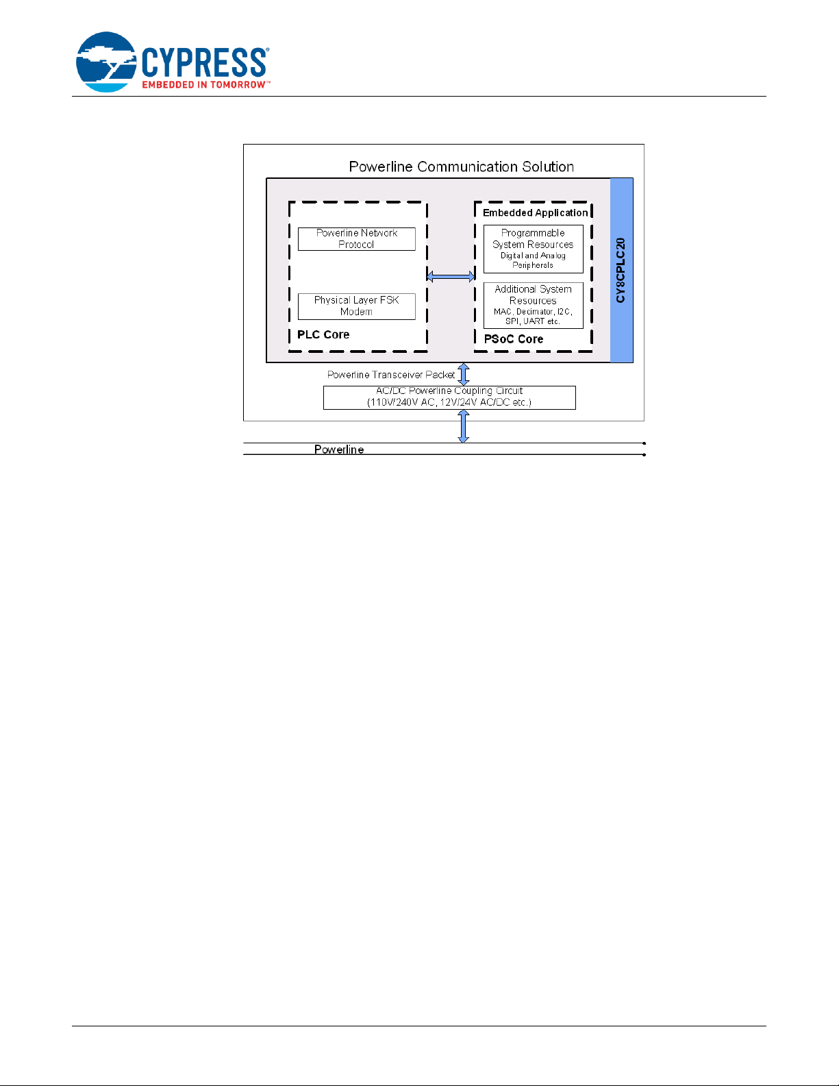
A block diagram of the PLC solution with the CY8CPLC20 programmable PLC chip is shown in Figure 1. To interface
the device to the powerline, a coupling circuit is required.
3.1 Transmit Signal Path......................................... 13
3.2 Receive Signal Path.......................................... 13
3.3 Signal Path Component Requirements ............. 14
3.4 Power Supply .................................................... 14
3.5 PLC Device Interface ........................................ 15
4 Summary ................................................................... 17
Document History ............................................................ 18
Worldwide Sales and Design Support ............................. 19
www.cypress.com Document No. 001-55427 Rev. *E 1
Page 2
Cypress Powerline Communication Board Design Analysis
Figure 1. Cypress PLC Solution Block Diagram
Cypress provides the CY3274 High Voltage Programmable PLC Development Kit (DVK) for evaluating the Cypress
PLC solution.
The CY3274 is designed with the filtering and power supply circuitry to operate on 110-240 V AC powerlines. They
are compliant to the following CENELEC and FCC standards:
Powerline Signaling (EN50065-1:2001, FCC Part 15)
Powerline Immunity (EN50065-2-1:2003,
EN61000-3-2/3)
Safety (EN60950)
The CY3274 kits are used to develop a powerline controller and embedded host application on the CY8CPLC20
Programmable PLC device. They contain many user interface options such as I2C, RS232, GPIO, analog voltage,
LCD display, and LED to develop a full application.
The following sections describe the design of the filter circuits and power supplies, including the selection of critical
components for meeting performance and compliance requirements.
2 High Voltage Board Design
This section describes the design of the high voltage (110 V AC to 240 V AC) PLC boardCY3274.
The design includes all circuitry to meet the requirements for signaling on high voltage lines according to the
EN50065-1:2001 standard. The high voltage boards include an isolated offline switch mode power supply accepting
input voltages in the range of 110-240 V AC, and 50-60 Hz line frequency, operating off the same powerlines that
carry the communication signaling.
The design contains transmit signal filtering and amplification to meet the conducted emissions requirements of the
CENELEC and FCC standards. It also has receive signal filtering and signal isolation external to the Cypress PLC
device. This provides a compact and low cost implementation that is adaptable to a wide variety of PLC applications.
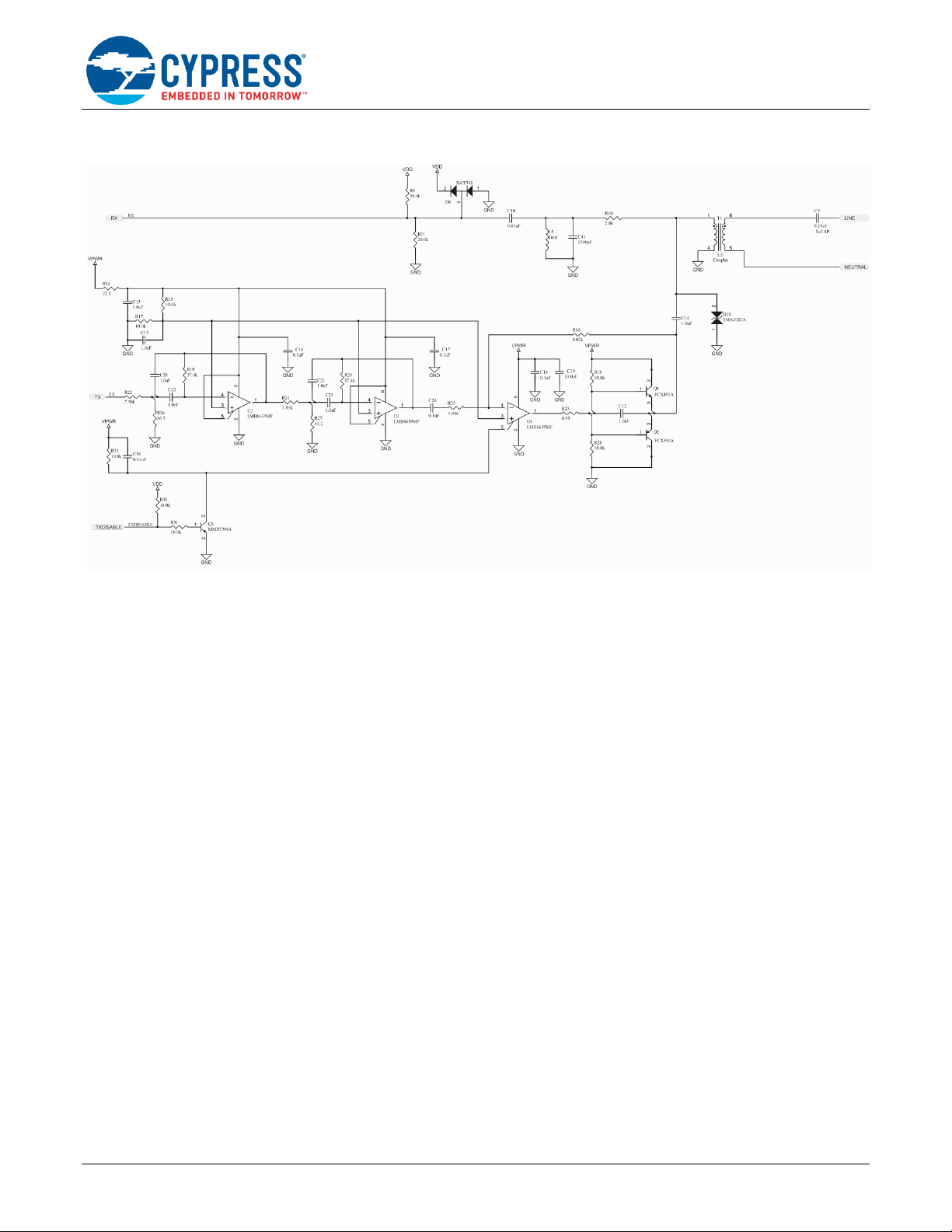
The schematic in Figure 2 shows the Cypress high voltage board’s transmit filter and amplification, receive filter, and
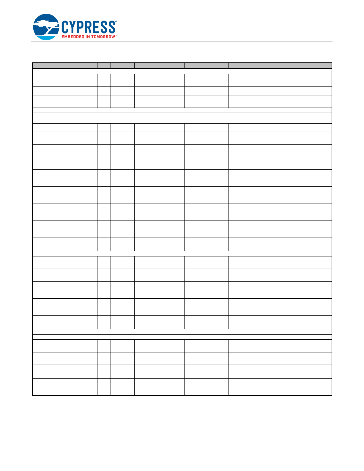
coupling circuit to the high voltage powerline. The Bill of Materials (BOM) of these components is listed in Table 1.
www.cypress.com Document No. 001-55427 Rev. *E 2
Page 3
Cypress Powerline Communication Board Design Analysis
Figure 2. Cypress High Voltage PLC Board Signal Filtering, Amplification, and Coupling Circuit
www.cypress.com Document No. 001-55427 Rev. *E 3
Page 4
Cypress Powerline Communication Board Design Analysis
Description
Designator
Qty.
Value
Manufacturer
Manufacturer Part#
Vendor
VPN
High Voltage Coupling Circuit
Capacitor Metal Poly
Film 0.15uF 300VAC
X1
C9 1 0.15 µF
Panasonic
ECQ-U3A154MG
Digikey
P11117-ND
Isolation
Transformer
T1 1
Precision Components, Inc.
0505-0821G
http://www.pcitransformers.com
Transient Voltage
Suppressor 400W
12V BIDIRECT SMA
D10 1
Micro Commercial Co
SMAJ12CA-TP
Digikey
SMAJ12CA-TPMSCT-ND
Transmitter Circuit
Transmit Amplification
Capacitor Ceramic
1.0uF 16V X7R 0603
C12, C13,
C14, C15
4
1.0 µF
Taiyo Yuden
EMK107B7105KA-T
Digikey
587-1241-1-ND
Capacitor Ceramic
0.10uF 10% 16V
X7R 0603
C18, C24
2
0.1 µF
Panasonic
ECJ-1VB1C104K
Digikey
PCC1762CT-ND
Capacitor Ceramic
10.0uF 10% 25V
X5R 1206
C19 1 10.0 µF
Taiyo Yuden
TMK316BJ106KL-T
Digikey
587-1337-1-ND
Capacitor Ceramic
0.01uF 25V X7R
0603
C36 1 0.01 µF
AVX
06033C103JAT2A
Digikey
06033C103JAT2A-ND
Transistor NPN HV
40V 1A SOT-89
Q1 1
Zetex
FCX491ATA
Digikey
FCX491ACT-ND
Transistor PNP HV
40V 1A SOT-89
Q2 1
Zetex
FCX591ATA
Digikey
FCX591ACT-ND
Transistor NPN
SOT-23
Q3 1
Fairchild
MMBT3904LT1
Digikey
MMBT3904LT1INCT-ND
Resistor 22.1 1%
1/10W 0603
R14 1 22.1
Yageo
RC0603FR-0722R1L
Digikey
311-22.1HRCT-ND
Resistor 10.0k 1%
1/10W 0603
R15, R17,
R18, R28,
R29, R30,
R31
7
10.0 k
Yageo
RC0603FR-0710KL
Digikey
311-10.0KHRTR-ND
Resistor 4.02k 1%
1/10W 0603
R16 1 4.02 k
Yageo
RC0603FR-074K02L
Digikey
311-4.02KHRCT-ND
Resistor 4.99 1%
1/10W 0603
R23 1 4.99
Yageo
RC0603FR-074R99L
Digikey
311-4.99HRCT-ND
Resistor 1.00k 1%
1/10W 0603
R25 1 1.00 k
Yageo
RC0603FR-071KL
Digikey
311-1.00KHRTR-ND
Op-Amp 190MHz
U4 1
National Semiconductor
LMH6639MF/NOPB
Digikey
LMH6639MFCT-ND
Transmit Filtering for FCC/CENELEC
Capacitor Ceramic
0.10uF 10% 16V
X7R 0603
C16, C17
2
0.1 µF
Panasonic
ECJ-1VB1C104K
Digikey
PCC1762CT-ND
Capacitor Ceramic
1000PF 1% 5V NP0
0603
C20, C21,
C22, C23
4
1.0 nF, 1%
AVX
06033A102FAT2A
Digikey
06033A102FAT2A-ND
Resistor 37.4k 1%
1/10W 0603
R19, R20
2
37.4 k
Yageo
RC0603FR-0737K4L
Digikey
311-37.4KHRCT-ND
Resistor 3.83k 1%
1/10W 0603
R21 1 3.83 k
Yageo
RC0603FR-073K83L
Digikey
311-3.83KHRCT-ND
Resistor 7.50k 1%
1/10W 0603
R22 1 7.50 k
Yageo
RC0603FR-077K5L
Digikey
311-7.50KHRTR-ND
Resistor 36.5 1%
1/10W 0603
R26 1 36.5
Yageo
RC0603FR-0736R5L
Digikey
311-36.5HRCT-ND
Resistor 41.2 1%
1/10W 0603
R27 1 41.2
Yageo
RC0603FR-0741R2L
Digikey
311-41.2HRCT-ND
Op-Amp 190MHz
U2, U3 2
National Semiconductor
LMH6639MF/NOPB
Digikey
LMH6639MFCT-ND
Receiver Circuit
Capacitor Ceramic
0.01uF 25V X7R
0603
C10 2 0.01 µF
AVX
06033C103JAT2A
Digikey
06033C103JAT2A-ND
Capacitor Ceramic
1500pF 10% 50V
X7R 0603
C41 1 1500 pF
Yageo
CC0603KRX7R9BB152
Digikey
311-1184-2-ND
Dual Schottky Diode
D6 1
ST Micro
BAT54SFILM
Digikey
497-2522-1-ND
Inductor 1mH 10%
1007
L5 1 1 mH
Taiyo Yuden
CB2518T102K
Digikey
587-2195-1-ND
Resistor 2.0k 1%
1/10W 0603
R10 1 2.0 k
Yageo
RC0603FR-072KL
Digikey
311-2.00KHRCT-ND
Resistor 20.0k 1%
1/10W 0603
R9, R11 2 20.0 k
Yageo
RC0603FR-0720KL
Digikey
311-20.0KHRCT-ND
Table 1. Cypress High Voltage PLC Board Signal Filtering, Amplification, and Coupling BOM
www.cypress.com Document No. 001-55427 Rev. *E 4
Page 5
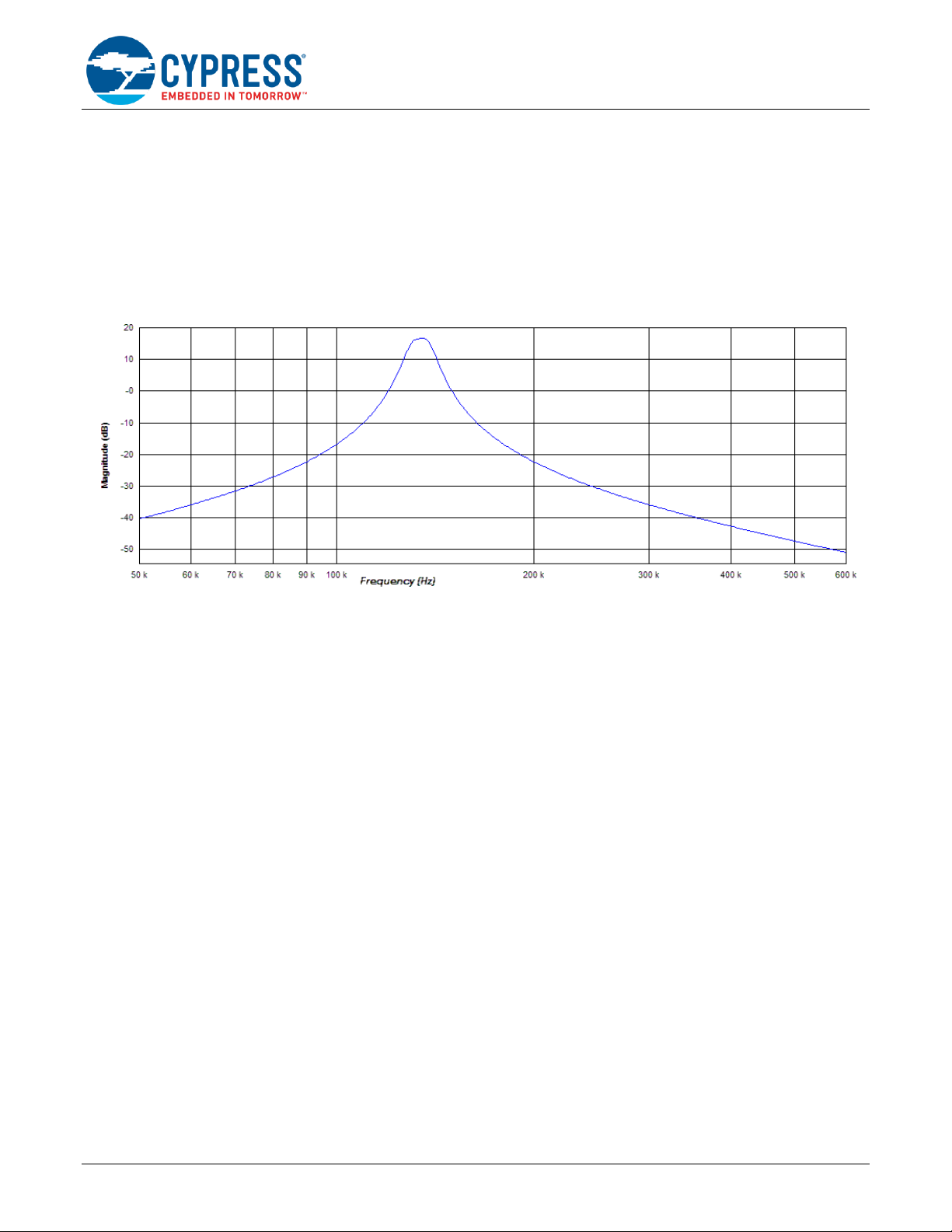
2.1 Transmit Signal Path
2.1.1 Transmit Filter
The FSK transmit signal TX is generated on the FSK_OUT pin of the Cypress PLC device as a low amplitude
(~125 mVp-p), unfiltered signal. This signal is applied to the input of an external transmit filter block consisting of
opamps U2 and U3, and their related passive components. The transmit filter is a fourth order Chebyshev response
band pass filter, designed for 1.5 dB maximum pass band ripple. It provides 16.5 dB of gain at the center frequency
of 133 kHz, suppression of -20 dBc at the 150 kHz band limit, and -50 dBc and -60 dBc at the second and third
carrier harmonics, respectively. The transmit filter response is shown graphically in Figure 3.
Figure 3. Cypress High Voltage PLC Board Transmit Filter Response
Cypress Powerline Communication Board Design Analysis
The power supply for the transmit filter opamps is a filtered version of the VPWR supply. This prevents the relatively
large currents produced by the power amplifier from feeding back into the high-Q filter circuit through the power
supply and causing oscillations. Hence, it is advisable to avoid routing the high current transmit signal near the filter
circuit.
2.1.2 Transmit Amplification
The filtered transmit data signal is applied to the power amplifier, which consists of opamp U4, transistors Q1 and Q2,
and associated passive components. The power amplifier provides an additional 12 dB voltage gain, and is capable
of driving low impedance loads presented by the powerline.
2.1.3 High Voltage Coupling
The transmit signal from the power amplifier is driven on to the powerlines via the isolation transformer T1. Capacitor
C14 provides DC isolation for the transmitter on the device side, and C9 provides line frequency isolation on the line
side.
When the device is not actively transmitting, the signal TX_DISABLE is asserted from the PLC device. This disables
the external power amplification circuitry to save power and make the transmit amplification circuit have a high
impedance so that the receive signal is not attenuated. Note that the transmit filter stage amplifiers U2 and U3 are
always enabled, so that there is no spurious noise output on the line due to filter ringing at startup.
www.cypress.com Document No. 001-55427 Rev. *E 5
Page 6
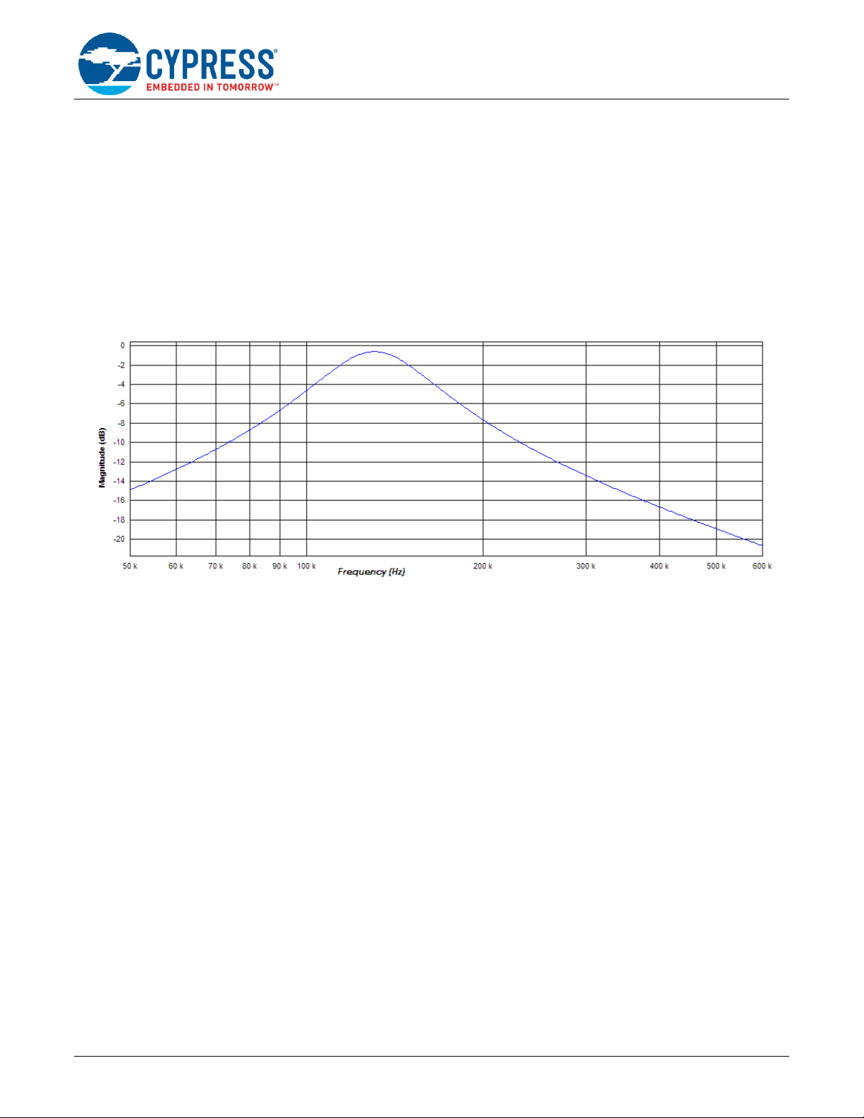
2.2 Receive Signal Path
The receive signal is coupled from the line into the kit via the same isolation transformer, T1, as is used by the
transmitter.
2.2.1 Receive Filter
Capacitor C10 provides DC isolation. Resistor R10 provides a signal input impedance for the receiver. This resistor,
in combination with D6, provides signal limiting to protect the receiver circuitry from high amplitude transmitter signals
and any large signals coupled in from the line. The receive filter comprised of L5 and C41, in combination with R10,
provides some rejection of out-of-band interference, such as AM broadcast signals. This interference may be coupled
from the line and would otherwise swamp the PLC device’s internal receiver circuitry. The response of the receive
filter is shown in Figure 4. Resistors R9 and R11 set the VCC/2 bias voltage required on the receive pin of the PLC
device.
Figure 4. Cypress High Voltage PLC Board Receive Filter Response
Cypress Powerline Communication Board Design Analysis
2.3 Signal Path Component Requirements
The values of the transmit filter passive components are relatively critical; 1% tolerance parts should be used to
ensure an accurate response. The opamps used in the transmit filter implementation must meet the following
requirements:
Gain Bandwidth (GBW) > 50 MHz
Voltage feedback
VDD - VSS ≥ 12 V
Power Supply Rejection Ration (PSRR) > 70 dB
Total Harmonic Distortion (THD) < -60 dB
The coupling transformer T1 must provide a low DC resistance (<0.5 ), low leakage inductance (<12 H) to
minimize signal loss and isolation, consistent with safety requirements per EN60950 specification. The signal
coupling transformer, T1, used in the CY3272 provides 3750 V isolation, a DC resistance of <0.35 and a leakage
inductance less than 1 H.
Capacitor C9 must be X1 or X2 rated to accommodate the turn-on surge, which occurs when power is applied to the
device, as well as surge immunity according to EN 61000-4-5 and EN 50065-2-1 standards. The capacitor C9, used
in the high voltage board design is a 300 V AC Panasonic ECQUG series metalized polyethylene film device, which is
rated for direct across-line application, accommodating the surge requirements of the previously mentioned
specifications.
www.cypress.com Document No. 001-55427 Rev. *E 6
Page 7

2.4 Power Supply
This section describes the power supply design for the high voltage boards. The schematic of the power supply is
shown in Figure 5. The BOM of the power supply is listed in Table 2.
The offline switch mode power supply on the high voltage boards is a standard isolated flyback converter. Bridge
rectifier D7 produces a rectified input from the AC line, which is used to drive the primary side of the converter.
Capacitors C30 and C31 provide charge storage to guarantee a sufficiently high input voltage to operate the
converter throughout the entire AC line cycle. C30 and C31, in combination with T3, minimize the conduction of
power supply switching transients onto the AC line. R41 provides in-rush current limiting.
Inductor L3 and capacitor C29 provide isolation to prevent the 133 kHz transmitter signal from riding the AC line
voltage into the rectifier, creating harmonic energy on the AC lines. The inductor also presents a high impedance to
the powerline so that the power supply does not load the PLC signal. These components provide an additional
measure of protection for both conducted immunity and conducted radiation.
An iWatt iW1690 power controller manages the power conversion. Startup current for the device is provided on its Vin
pin via resistors R32 and R34. When it starts operating, power and regulation voltage sensing is provided to the
controller by the auxiliary secondary winding of T2.
Cypress Powerline Communication Board Design Analysis
Figure 5. Cypress High Voltage PLC Board Power Supply Circuit
www.cypress.com Document No. 001-55427 Rev. *E 7
Page 8
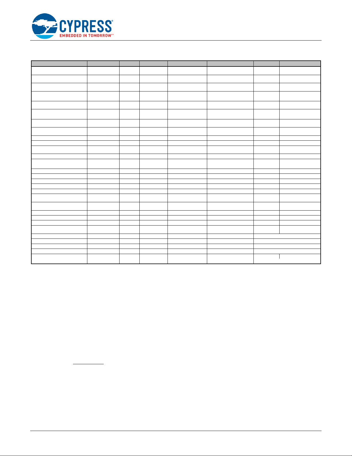
Cypress Powerline Communication Board Design Analysis
Description
Designator
Quantity
Value
Manufacturer
Manufacturer Part#
Vendor
VPN
Capacitor Ceramic 10.0uF 10%
25V X5R 1206
C26, C33 2 10.0 µF
Taiyo Yuden
TMK316BJ106KL-T
Digikey
587-1337-1-ND
Capacitor Ceramic 0.10uF 10%
16V X7R 0603
C27, C34 2 0.1 µF
Panasonic
ECJ-1VB1C104K
Digikey
PCC1762CT-ND
Capacitor Ceramic 470PF
250VAC X1Y1 RAD
C28 1 470 pF
TDK
CD95-B2GA471KYNS
Digikey
445-2407-ND
Capacitor Metal Poly Film
0.022uF 300VAC X1
C29 1 0.022 µF
Panasonic
ECQ-U3A223MG
Digikey
P11112-ND
Capacitor Electrolytic 4.7uF,
400V
C30, C31
2
4.7 µF, 400 V
Nichicon
UVR2G4R7MPD
Digikey
493-1229-ND
C30, C31 (2nd
source, 105C)
4.7 µF, 400 V
United Chemi-Con
EKMG401ELL4R7MJ16S
Digikey
565-1411-ND
Capacitor Electrolytic 330uF
16V 20%
C32 1 330 µF, 16 V
Nichicon
UPW1C331MPD
Digikey
493-1784-ND
Capacitor Electrolytic 10uF 50V
20%
C35 1 10 µF, 50 V
Nichicon
UPW1H100MDD
Digikey
493-1890-ND
Full Wave Diode Bridge
D7 1
Fairchild
DF10S
Digikey
DF10SCT-ND
Schottky Diode 100V 1A SMA
D8, D9 2
Diodes Inc
B1100-13-F
Digikey
B1100-FDICT-ND
Inductor 1500uH 0.2A 5%
Radial
L3 1 1.5 mH
Taiyo Yuden
LHL08TB152J
Digikey
LHL08TB152J-ND
Inductor 22uH 20% 1210
L4 1 22 uH
Taiyo Yuden
CBC3225T220MR
Digikey
587-1626-1-ND
NPN Silicon Planar Medium
Power High-Gain Transistor
Q4 1
TSC
TS13003HVCT
mouser.com
821-TS13003HVCT
Q4 (2nd Source)
ST Micro
STX616-AP
Digikey
497-7625-1-ND
Resistor 750k 1% 1206
R32 1 750 k, 1%
Yageo
RC1206FR-07750KL
Digikey
311-750KFRCT-ND
Resistor 10.0k 1% 1/10W 0603
R33 1 10.0 k
Yageo
RC0603FR-0710KL
Digikey
311-10.0KHRTR-ND
Resistor 820k 1% 1206
R34 1 820 k, 1%
Yageo
RC1206FR-07820KL
Digikey
311-820KFRCT-ND
Resistor 3.9 Ohm 1% 0805
R35 1 3.9
Yageo
RC0805FR-073R9L
Digikey
311-3.90CRCT-ND
Resistor 68.0k Ohm 1/8W 1%
0805
R36 1 68k, 1%
Yageo
RC0805FR-0768KL
Digikey
311-68.0KCRTR-ND
Resistor 1.00 Ohm 1/10W 1%
0603
R37 1 1.0
Yageo
RC0603FR-071RL
Digikey
311-1.00HRCT-ND
Resistor 100k 1/10W 1% 0603
R38 1 100 k
Yageo
RC0603FR-07100KL
Digikey
311-100KHRTR-ND
Resistor 12.0K 1/10W 1% 0603
R39 1 12 k, 1%
Yageo
RC0603FR-0712KL
Digikey
311-12.0KHRCT-ND
Resistor 6.8k, 1% 0603
R40 1 6.8 k, 1%
Yageo
RC0603FR-076K8L
Digikey
311-6.80KHRTR-ND
RESISTOR 10.0 OHM 5W 5%
WIREWND
R41 1 10, 5 W
Vishay
AC05000001009JAC00
Digikey
PPC5W10.0CT-ND
Power Trasnsformer EE-16
T2 1 3.2 mH
Shenzen Goldenway
EE-16 (5+5) (rev-A)
e-mail:sales@greensmps.com
T2 (2nd Source)
Renco Electronics
RLCY-1014
e-mail:sales@rencousa.com
24mH Common Mode Choke
T3 1 24 mH
Shenzen Goldenway
EE8.3(2+2)-hori, (rev-A)
e-mail:sales@greensmps.com
T3 (2nd Source)
Renco Electronics
RLCY-1013
e-mail:sales@rencousa.com
Voltage Regulator 5 Volt
U5 1
ST Micro
LD1117S50CTR
Digikey
497-1243-1-ND
Off-Line Switcher
U6 1
iWatt
iW1690-07
e-mail:sales@iwatt.com
)1(**D
VinND
Vout
Table 2. Cypress High Voltage PLC Board Power Supply BOM
Switching transistor Q4 is operated directly by the iW1690. Switch current is sensed across resistor R35. The
switching frequency of the iW1690 is approximately 75 kHz. The basic cycle-by-cycle operation of the power
converter is described briefly in the following paragraph.
With Q4 switched ON, current is pulled from the line through the primary winding of T2. Diodes D8 and D9 ensure
that the secondary windings of T2 do not conduct current during the switch ON time and energy is stored in the
magnetic field of T2. With Q4 switched OFF, the voltage polarity across the primary and secondary windings of T2 is
reversed, causing D8 and D9 to be forward biased. Current now flows in the secondary windings, delivering energy to
the loads. Bulk filter capacitance is provided on the main secondary output by C32. The auxiliary secondary output is
filtered at C35 to power the controller. The auxiliary secondary voltage is monitored by the converter at its Vsense
pin. This voltage is used to implement output secondary voltage regulation by setting the switch duty cycle.
The voltage on each of the rectified secondary outputs is determined by the primary voltage, the turns ratio of the
transformer, and the switch duty cycle, as follows:
Equation 1
www.cypress.com Document No. 001-55427 Rev. *E 8
Page 9

Where, N is the secondary or primary turns ratio and D is the switch duty cycle. The nominal turns ratio for both
)1( D
Vin
Vpk
secondaries of T2 is 0.13. As the input voltage varies over the course of an AC line cycle, the power controller varies
D to maintain a constant voltage on the secondary supplies. Because the voltages of the secondary outputs are
related by the turns ratios, it is possible to regulate multiple, isolated outputs by monitoring just one of the
secondaries. In this case, the controller regulates the main output by monitoring its own supply winding. The voltage
produced at C32 is approximately 10 V. This voltage is filtered via L4/C33 to further reduce switching noise and
produce the VPWR supply, which drives the transmitter circuitry. The 10 V supply is also applied to the input of linear
regulator U5, which produces a 5 V VDD power supply for the Cypress PLC device and optionally, an external
controlling device.
2.5 Power Path Component Requirements
The power converter is designed for worldwide operation and is expected to operate from line voltages ranging from
90-240 V AC. This results in peak voltages approaching 350 V DC, and hence, filter capacitors C30 and C31 must be
rated to accommodate these peak voltages.
In the flyback (Q4 OFF) state, the peak voltage generated on the primary winding of T2 (the collector of Q4), strictly
as a result of the circuit operation, is higher than Vin. This voltage is given as follows:
Equation 2
In addition, transformer leakage inductance results in an additional increase, above Vpk, at Q4 turn off. This results in
peak voltages approaching 500 V being possible at the collector of Q4.
Resistor R41 should be a high power rated (≥ 3 W), wire wound resistor that can support the surge requirements of
the system.
Capacitor C29 must be X1 or X2 rated to accommodate the turn on surge, which occurs when power is applied to the
device, as well as surge immunity according to EN 61000-4-5 and EN 50065-2-1. The capacitor used in the high
voltage board design is a 300 V AC Panasonic ECQUG series metalized polyethylene film device, which is rated for
direct across-line application. It accommodates the surge requirements of the specifications mentioned earlier.
L3 should be rated for ≥ 0.2 A of current.
Capacitor C28 must be a Y1-rated safety capacitor. The capacitor used in the high voltage board design is a 4000 V
AC TDK CD series mid-high voltage ceramic device. This device is rated for direct line-ground applications and
accommodates the surge requirements of the previously mentioned specifications.
It is important to note that a bleeder resistor may need to be used, depending on the discharge path for the PLC
coupling capacitor C9. When power is disconnected, this capacitor will still be charged unless it can discharge
through the power supply. In the Cypress high voltage boards, it was tested that the voltage discharges quickly
enough to meet the safety requirements of CENELEC EN60950. However, other power supplies may not discharge
the voltage quickly enough and in that case, a bleeder resistor (> 1 M 0.25 W, working voltage >360 V DC) should
be used.
Cypress Powerline Communication Board Design Analysis
2.5.1 Protection Circuit
Basic protection against line transients is provided by transient suppressor D1. The high voltage boards employ a
Panasonic ZNR type device with a peak surge current capability in excess of 1000 A and a voltage rating of 275 V
AC. This type of device has the advantage of low shunt capacitance, 120 pF in this case, which ensures that it does
not degrade the PLC signal. Protection against catastrophic circuit failure is provided by fuse F1, which is a 2 A, 250
V AC Slow-Blow device. This protection circuit is shown in Figure 6 and the BOM is listed in Table 3.
www.cypress.com Document No. 001-55427 Rev. *E 9
Page 10
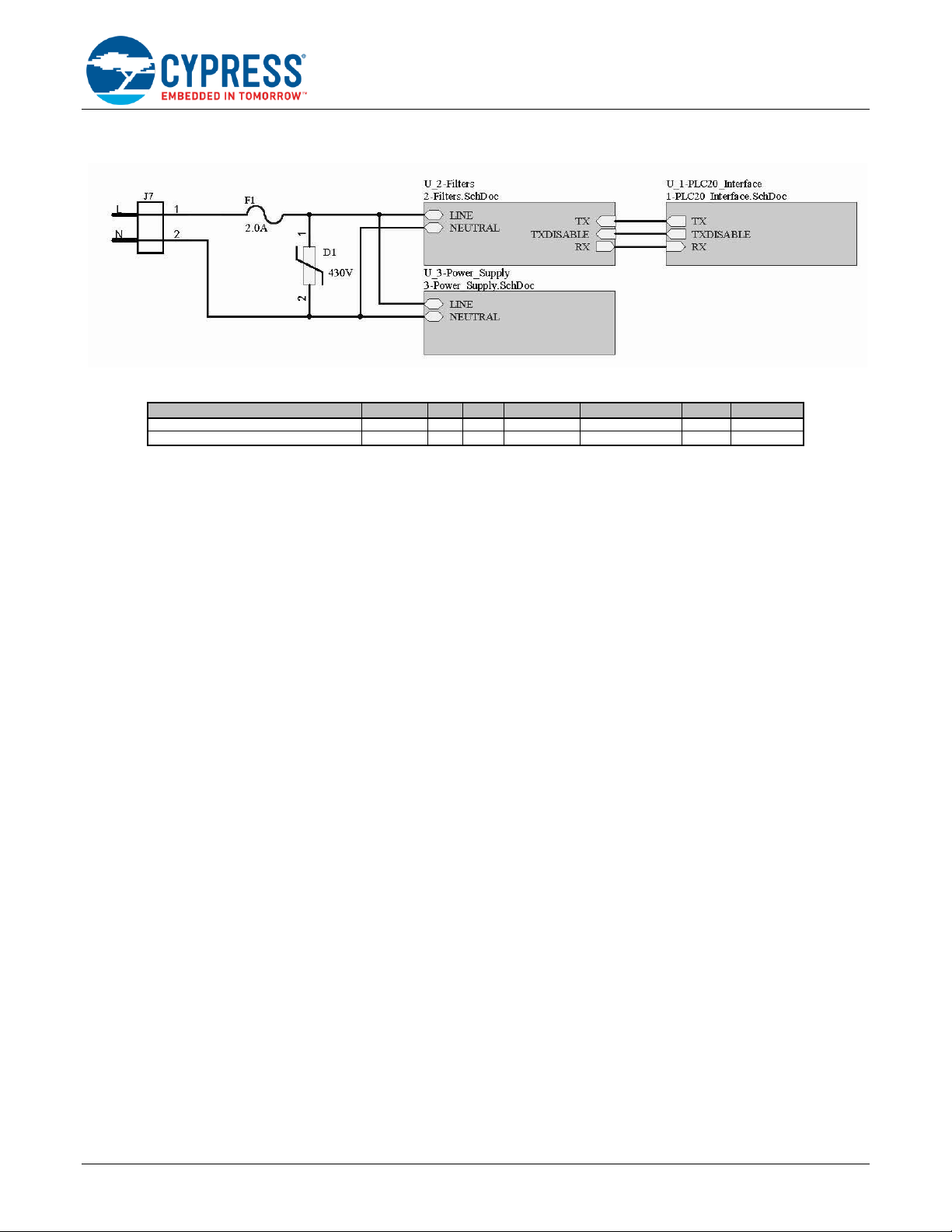
Figure 6. Cypress High Voltage PLC Board AC Line Input Protection Circuit
Description
Designator
Qty.
Value
Manufacturer
Manufacturer Part#
Vendor
VPN
Transorb Voltage Suppressor 430V 1250A ZNR
D1 1 430 V
Panasonic
ERZ-V07D431
Digikey
P7251-ND
Fuse 2A Slow Blow 250VAC
F1 1 2.0 A
Bel Fuse
RST 2
Digikey
507-1179-ND
Table 3. Cypress High Voltage PLC Board AC Line Input Protection BOM
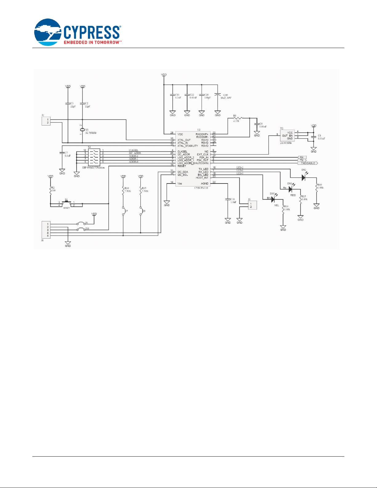
2.6 PLC Device Interface
This section describes the circuitry that is directly connected to the Cypress PLC device (U1) and not part of the
transmitter and receiver circuitry described above. In the schematic shown in Figure 7, there are many components
shown that are not required for the final system, but are useful for status indication and debugging. The BOM for this
circuit is shown in Table 4. It separates the required components from the optional components.
The 32.768 kHz crystal (Y2) is required for PLC communication because it is used for the precise timing of the
network protocol and if selected, is also used for the timing of the FSK modulator and demodulator. On the other
hand, the 24.00 MHz oscillator (Y1) is not required in most designs. It is provided as an optional clock source for
timing the FSK modulator and demodulator because it generates a tighter frequency spectrum, which may help with
designs that are marginal to meeting the FCC or CENELEC conducted emissions requirements. The selection
between the FSK modem source is made by setting the CLKSEL pin (‘1’ = 32.768 kHz crystal,
‘0’ = 24.00 MHz oscillator, internal pull-up).
Resistor R2 and capacitor C3 form a low pass filter that is used to filter the received 2400 bps demodulated signal,
which is output on pin RXCOMP+. The filtered signal is then connected to the pin RXCOMP-, where it is further
filtered and then deserialized.
Capacitors C1 and C2 are used for decoupling noise from the power supply. Similarly, C5 provides a cleaner signal
from the crystal to the device, and C6 provides a cleaner internal analog ground reference for the modem.
The I2C interface requires pull-up resistors on the bus. If the external host does not have pull-up resistors, then R6
and R7 should be used. The recommended value for these resistors is 2.4-7.5 k.
The LEDs are optional for PLC status indication (DS2 = receiving, DS3 = transmitting, DS4 = band-in-use detection)
and power indication (DS5). The resistors (R1, R3, R4, R5) associated with these LEDs are for current limiting.
The DIP switch bank S1 is optional for setting the device’s PLC address and I2C address, as well as selecting the
modem’s clock source.
Push-button S2 with current-limiting resistor R8 is optional and is used to easily reset the device to the default state,
instead of disconnecting and reconnecting power.
Cypress Powerline Communication Board Design Analysis
www.cypress.com Document No. 001-55427 Rev. *E 10
Page 11

Cypress Powerline Communication Board Design Analysis
Description
Designator
Qty.
Value
Manufacturer
Manufacturer Part#
Vendor
VPN
Discretes and Crystal
Capacitor Ceramic 0.10uF 10% 16V X7R 0603
C1, C5 2 0.1 µF
Panasonic
ECJ-1VB1C104K
Digikey
PCC1762CT-ND
Capacitor Ceramic 1.0nF X7R 10% 25V C0603
C2 1 1.0 nF
Murata
GRM033R71E102KA01D
Digikey
490-3184-1-ND
Capacitor Ceramic 0.01uF 25V X7R 0603
C3, C4 2 0.01 µF
AVX
06033C103JAT2A
Digikey
06033C103JAT2AND
Capacitor Ceramic 1.0uF 16V X7R 0603
C6 1 1.0 µF
Taiyo Yuden
EMK107B7105KA-T
Digikey
587-1241-1-ND
Capacitor Ceramic 22pF 100V C0G 0603
C7, C8 2 22 pF
Murata
GRM1885C2A220JA01D
Digikey
490-1335-1-ND
Resistor 2.1k 1% 1/10W 0603
R2 1 2.10 k
Yageo
RC0603FR-072K1L
Digikey
311-2.10KHRTRND
Crystal 32.768kHz 12.5pF
Y2 1 32.768 kHz
ECS Inc.
ECS-3X8X
Digikey
X1123-ND
I2C, Jumpers, and LEDs (Optional)
LED Red Clear 0805
DS2 1
Lite-On
LTST-C170KRKT
Digikey
160-1415-1-ND
LED Green Clear 0805
DS3 1
Lite-On
LTST-C170KGKT
Digikey
160-1414-1-ND
LED Yellow Clear 0805
DS4 1
Lite-On
LTST-C170KSKT
Digikey
160-1416-1-ND
Header 2-Pin 0.1 Centers
J1, J2, J3, J4, P1,
P2
6 Sullins
PEC02SAAN
Digikey
S1012E-02-ND
Header 5-Pin Locking 0.1Centers
J6 1
Amp/Tyco
640456-5
Digikey
A19471-ND
Resistor 1.00k 1% 1/10W 0603
R1, R3, R4 3 1.00 k
Yageo
RC0603FR-071KL
Digikey
311-1.00KHRTRND
Resistor 2.70k 1% 1/10W 0603
R6, R7 2 2.70 k
Yageo
RC0603FR-072K7L
Digikey
311-2.70KHRTRND
Resistor 330 1% 1/10W 0603
R8 1 330
Yageo
RC0603FR-07330RL
Digikey
311-330HRCT-ND
Resistor 402 1% 1/10W 0603
R5 1 402
Yageo
RC0603FR-07402RL
Digikey
311-402HRTR-ND
DIP Switch 5 Position DIP-5
S1 1
E-Switch
KAJ05LAGT
Digikey
EG4429-ND
Pushbutton N.O.
S2 1
E-Switch
TL3301AF160QG
Digikey
EG2526CT-ND
Oscillator
Y1 1 24.00 MHz
Crystek
C3290-24.000
Digikey
C3290-24.000-ND
Y1 (2nd Source)
24.00 MHz
Citizen
CSX750FCC24.000M-UT
Digikey
300-7214-2-ND
Figure 7. Cypress PLC Device Interface Circuit (on the High Voltage Board)
Table 4. Cypress PLC Device Interface BOM (on the High Voltage Board)
www.cypress.com Document No. 001-55427 Rev. *E 11
Page 12
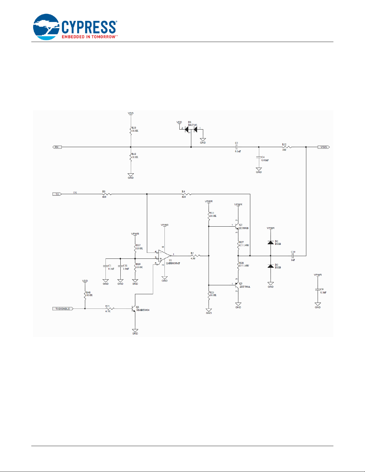
3 Low Voltage Board Design
This section describes the design of the boards meant for low voltage PLC. These boards are designed to operate on
12-24 V AC/DC powerlines. They are also designed to be low cost and robust systems that do not need to meet any
CENELEC or FCC compliance standards. The schematic in Figure 8 shows the Cypress low voltage board’s transmit
amplification, receive filter, and coupling circuit to the low voltage powerline. The BOM for designing such a board is
listed in Table 5.
Figure 8. Low Voltage PLC Board Signal Filter, Amplification, and Coupling Circuit
Cypress Powerline Communication Board Design Analysis
www.cypress.com Document No. 001-55427 Rev. *E 12
Page 13
Cypress Powerline Communication Board Design Analysis
Description
Designator
Qty.
Value
Manufacturer
MFGPN
Vendor
VPN
Low Voltage Coupling Circuit
Capacitor Ceramic 10uF 35V X5R 10% 1206
C30 1 10 µF
Murata
GRM31CR6YA106KA12L
Digikey
490-5524-1-ND
Ferrite Chip 100 Ohm 4A 0805
L2 1
TDK
MPZ2012S101A
Digikey
445-1567-1-ND
Inductor Power Unshielded 470uH SMD
L3 1 470 uH
Pulse
P0752.474NLT
Digikey
553-1071-1-ND
Transmitter Circuit
Capacitor Ceramic 0.1uF 25V X7R 0603
C1 1 0.1 µF
AVX
06033C104JAT2A
Digikey
478-3713-1-ND
Capacitor Ceramic 0.1uF 25V X7R 0603
C9 1 0.1 µF
AVX
06033C104JAT2A
Digikey
478-3713-1-ND
Capacitor Ceramic 10uF 16V X5R 1206
C10 1 10 µF
TDK
C3216X5R1C106K
Digikey
445-4052-1-ND
Capacitor Ceramic 1UF 50V Y5V 0805
C31 1 1.0 µF
Murata
GRM21BF51H105ZA12L
Digikey
490-3903-1-ND
Diode Ultrafast 100V 1A
D2, D3
2
ES1B
Diodes Inc.
ES1B
Digikey
ES1B-FDICT-ND
Transistor NPN SOT-23
Q1 1 MMBT3904
Fairchild
MMBT3904LT1
Digikey
MMBT3904LT1INCT-ND
Transistor NPN 45V 3A
Q2 1 ZXT690B
Zetex
ZXT690BKTC
Digikey
ZXT690BKCT-ND
Transistor PNP 40V 3A
Q3 1 ZXT790A
Zetex
ZXT790AKTC
Digikey
ZXT790AKCT-ND
Resistor 620 OHM 1/10W 1% 0603 SMD
R3, R4
2
620
Rohm
MCR03EZPFX6200
Digikey
RHM620HCT-ND
Resistor 4.99 1% 1/10W 0603
R5 1 4.99
Yageo
RC0603FR-074R99L
Digikey
311-4.99HRCT-ND
Resistor 10.0k 1% 1/10W 0603
R13, R23, R37,
R39, R48
5
10.0 k
Rohm
MCR03EZPFX1002
Digikey
RHM10.0KHCT-ND
Resistor 4.70K OHM 1/10W 1% 0603 SMD
R25 1 4.7 k
Yageo
RC0603FR-074K7L
Digikey
311-4.70KHRCT-ND
Resistor 0.5 1% 1/4W 0805
R27, R28
2
0.5 1/4 W
Susumu
RL1220S-R50-F
Digikey
RL12S.50FCT-ND
Op-Amp 190MHz
U1 1 LMH6639MF
National
Semiconductor
LMH6639MF/NOPB
Digikey
LMH6639MFCT-ND
Receiver Circuit
Capacitor Ceramic 1500pF 10% 50V X7R 0603
C4 1 1500 pF
Yageo
CC0603KRX7R9BB152
Digikey
311-1184-2-ND
Capacitor Ceramic 0.01uF 25V X7R 0603
C5 1 0.01 µF
AVX
06033C103JAT2A
Digikey
06033C103JAT2A-ND
Diode Schottky 40V 0.3A SOT-23
D1 1 BAT54S
ST Micro
BAT54SFILM
Digikey
497-2522-1-ND
Inductor 1mH 10% 1007
L5 1 1 mH
Taiyo Yuden
CB2518T102K
Digikey
587-2195-1-ND
Resistor 10.0k 1% 1/10W 0603
R33, R43
2
10.0 k
Rohm
MCR03EZPFX1002
Digikey
RHM10.0KHCT-ND
Resistor 2.0k 1% 1/10W 0603
R52 1 2.0 k
Yageo
RC0603FR-072KL
Digikey
311-2.00KHRCT-ND
Table 5. Low Voltage PLC Board Signal Filter, Amplification, and Coupling Circuit BOM
3.1 Transmit Signal Path
3.1.1 Transmit Amplification
The FSK transmit signal TX is generated on the FSK_OUT pin of the Cypress PLC device as a higher amplitude
(approximately 1.55 Vp-p), unfiltered signal. The low voltage boards do not have any transmit filtering, which reduces
the BOM cost. There is one output amplification stage, implemented using op-amp U1 and transistors Q2 and Q3, to
drive the low impedance load presented by the powerline. Resistors R3 and R4 set a gain of 1x.
When the device is not actively transmitting, it asserts the signal TX_DISABLE. This disables the external power
amplification circuitry to save power. This also makes the transmit amplification circuit have a high impedance so that
the receive signal is not attenuated.
3.1.2 Low Voltage Coupling
The transmit signal from the power amplifier is driven on to the powerlines via chip bead L2. Capacitor C6 provides
DC isolation for the transmitter on the device side. Capacitor C30 provides line frequency isolation on the line side.
With inductor L3, capacitor C30 provides a filter to remove out-of-band noise from entering the receiver.
3.2 Receive Signal Path
The receive signal is coupled from the line into the low voltage boards via the same chip bead L2, as is used by the
transmitter.
3.2.1 Receive Filter
Capacitor C5 provides DC isolation. Resistor R52 provides a signal input impedance for the receiver. This, in
combination with D6, provides signal limiting to protect the receiver circuitry from the relatively high amplitude
transmitter signals, including any large signals coupled in from the line. The receive filter comprised of R52, L5, and
C4, provides some rejection of out-of-band interference such as AM broadcast signals. This interference may be
coupled from the line, and may otherwise swamp the PLC device’s internal receiver circuitry. Resistors R33 and R43
set the VCC/2 bias voltage required on the receive pin of the PLC device.
www.cypress.com Document No. 001-55427 Rev. *E 13
Page 14

3.3 Signal Path Component Requirements
The chip bead L2 is designed specifically for powerline applications and provides a low DC resistance (0.02 ) and
high current handling capability (3 A). Its impedance curve is similar to that of a 0.4 H inductor. The transmit
capacitors C10 and C30 should be sized so that they match the impedance of the inductor as closely as possible.
This reduces the transmit impedance, which increases the driving distance of the system. In this case, C10 and C30
are each 10 F, which yields an equivalent capacitance of 5 F. At 132 kHz, the impedance of this equivalent
capacitor matches the inductor to within 0.1 . Capacitor C30 must also be rated to be above the maximum voltage
on the powerline.
The opamp U1 used in the transit amplifier section must provide both high speed to minimize crossover distortion,
and relatively high output currents to drive the output transistors.
3.4 Power Supply
This section describes the power supply design for low voltage boards. The schematic of the power supply is shown
in Figure 9 and the BOM for the power supply is listed in Table 6.
Inductor L4 provides high impedance to the powerline so that the power supply does not load the PLC signal. It
should be rated to ≥ 200 mA.
Resistor R2 limits in-rush current. It should be rated to ≥ 1 W.
D9 protects the circuit from voltage transients and D10 rectifies the voltage when AC power is present.
Regulator U7 provides a 5 V output, which is used for the PLC device and the transmit amplifier.
The 100 µF electrolytic capacitor C24, along with a 10 µF tantalum capacitor and two 0.1 µF ceramic capacitors
provide the necessary decoupling for the PLC device, considering the 5 V supply is shared with the transmit amplifier.
Figure 9. Power Supply Circuit while designing Low Voltage PLC Board
Cypress Powerline Communication Board Design Analysis
www.cypress.com Document No. 001-55427 Rev. *E 14
Page 15

Table 6. Power Supply BOM for Low Voltage PLC Board
Description
Designator
Qty.
Value
Manufacturer
MFGPN
Vendor
VPN
Capacitor Electrolytic 100uF 10V Aluminum Radial
C24 1 100 µF
PANASONIC
ECA-1AM101
Digikey
P5123-ND
Capacitor Electrolytic 220uF 50V
C25 1 220 µF
PANASONIC
ECA-1HM221
Digikey
P5183-ND
Diode Transorb 33V 600W BI-DIR SMB
D9 1
Littelfuse
SMBJ33CA
Digikey
SMBJ33CALFCT-ND
Diode Ultrafast 100V 1A
D10 1 ES1B
Diodes Inc.
ES1B
Digikey
ES1B-FDICT-ND
Inductor Power Unshielded 470uH SMD
L4 1 470 uH
Pulse
P0752.474NLT
Digikey
553-1071-1-ND
Resistor 715 OHM 1/10W 1% 0603 SMD
R45 1 715
Rohm
MCR03EZPFX7150
Digikey
RHM715HCT-ND
Resistor 240 OHM 1/10W 1% 0603 SMD
R46 1 240
Rohm
MCR03EZPFX2400
Digikey
RHM240HCT-ND
Resistor 10 Ohm 1W 5% Metal Oxide
R54 1 10, 1 W
Stackpole
RSMF 1 10 5% R
Digikey
RSMF110JRCT-ND
Voltage Regulator 5 Volt
U7 1 LM317MDT
ST Micro
LM317MDT-TR
Digikey
497-1574-1-ND
3.5 PLC Device Interface
This section describes the circuitry directly connected to the Cypress PLC device (U2) and not part of the transmitter
and receiver circuitry described above. In the schematic shown in Figure 10, there are many components shown that
are not required for the final system. However, they are useful for status indication and debugging. The BOM for this
circuit is shown in Table 7. It separates the required components from the optional components. Note that the key
components are the same as for the high voltage board, except that the component numbering is different.
The 32.768 kHz crystal (Y1) is required for PLC communication because it is used for the precise timing of the
network protocol and if selected, is also used for the timing of the FSK modulator and demodulator. On the other
hand, the 24.00 MHz oscillator (Y2) is not required in most designs. It is provided as an optional clock source for
timing the FSK modulator and demodulator because it generates a tighter frequency spectrum, which may help with
designs that are marginal to meeting the FCC or CENELEC conducted emissions requirements. The selection
between the FSK modem source is made by setting the CLKSEL pin (‘1’ = 32.768 kHz crystal,
‘0’ = 24.00 MHz oscillator, internal pull-up).
Resistor R9 and capacitor C6 form a low pass filter that is used to filter the received 2400 bps demodulated signal,
which is output on pin RXCOMP+. The filtered signal is then connected to the pin RXCOMP-, where it is furthered
filtered and then deserialized.
Capacitors C11, C22, C26, and C39 are used for decoupling noise from the power supply. Similarly, C7 provides a
cleaner signal from the crystal to the device, and C18 provides a cleaner internal analog ground reference for the
modem.
The I2C interface requires pull-up resistors on the bus. If the external host does not have pull-up resistors, then R35
and R36 should be used. The recommended value for these resistors is 2.4-7.5 k.
The LEDs are optional for PLC status indication (DS2 = receiving, DS3 = transmitting, DS4 = band-in-use detection).
The resistors (R15, R16, and R49) associated with these LEDs are for current limiting.
The DIP switch bank S2 is optional for setting the device’s PLC address and I2C address, as well as selecting the
modem’s clock source. Push-button S1 with current-limiting resistor R2 is optional and is used to easily reset the
device to the default state, instead of disconnecting and reconnecting power.
Cypress Powerline Communication Board Design Analysis
www.cypress.com Document No. 001-55427 Rev. *E 15
Page 16
Cypress Powerline Communication Board Design Analysis
Figure 10. PLC Device Interface Circuit (on the Low Voltage Board)
www.cypress.com Document No. 001-55427 Rev. *E 16
Page 17
Cypress Powerline Communication Board Design Analysis
Description
Designator
Qty.
Value
Manufacturer
MFGPN
Vendor
VPN
Discretes and Crystal
Capacitor Ceramic 22pF 100V C0G 0603
C2, C3
2
22 pF
Murata
GRM1885C2A220JA01D
Digikey
490-1335-1-ND
Capacitor Ceramic 0.01uF 25V C0G 5% 0603
C6 1 0.01 µF
TDK
C1608C0G1E103J
Digikey
445-2664-1-ND
Capacitor Ceramic 0.1uF 25V X7R 0603
C7 1 0.1 µF
AVX
06033C104JAT2A
Digikey
478-3713-1-ND
Capacitor Ceramic 0.01uF 25V X7R 0603
C8 1 0.01 µF
AVX
06033C103JAT2A
Digikey
06033C103JAT2A-ND
Capacitor Ceramic 0.1uF 25V X7R 0603
C11 1 0.1 µF
AVX
06033C104JAT2A
Digikey
478-3713-1-ND
Capacitor Ceramic 1.0uF 16V X7R 0603
C18 1 1.0 µF
PANASONIC
ECJ-1V41E105M
Digikey
PCC2354CT-ND
Capacitor Ceramic 0.01uF 25V C0G 5% 0603
C22 1 0.01 µF
TDK
C1608C0G1E103J
Digikey
445-2664-1-ND
Capacitor Ceramic 100pF 25V X7R 0603
C26 1 100 pF
AVX
06031A101JAT2A
Digikey
478-1146-1-ND
Capacitor 10uF,10V
C39 1 10 µF, 10 V
Vishay
293D106X9010A2TE3
Digikey
718-1121-1-ND
Resistor 2.1k 1% 1/10W 0603
R9 1 2.10k
Rohm
MCR03EZPFX2101
Digikey
RHM2.10KHCT-ND
Power Line Controller
U2 1 CY8CPLC10
Cypress
Semiconductor
CY8CPLC10
Digikey
CY8CPLC10-28PVXI-ND
Crystal 32.768kHz 12.5pF
Y1 1 32.768 kHz
ECS Inc.
ECS-3X8X
Digikey
X1123-ND
I2C, Jumpers, and LEDs (Optional)
LED Blue
DS1 1 Blue
Rohm
SML-E12BC7TT86
Digikey
511-1589-1-ND
LED Green Clear 0805
DS2 1 LTST-C170KGKT
Lite-On
LTST-C170KGKT
Digikey
160-1414-1-ND
LED Red Clear 0805
DS3 1 LTST-C170KRKT
Lite-On
LTST-C170KRKT
Digikey
160-1415-1-ND
LED Yellow Clear 0805
DS5 1 LTST-C170KSKT
Lite-On
LTST-C170KSKT
Digikey
160-1416-1-ND
Header, 2-Pin
J1 1
MOLEX
09-65-2028
Digikey
WM18823-ND
Header 2-Pin 0.1 Centers
J2 1
Sullins
PEC02SAAN
Digikey
S1012E-02-ND
Header 2-Pin 0.1 Centers
J3, J6, J7, J9,
J10 5
Sullins
PEC02SAAN
Digikey
S1012E-02-ND
Power Jack 2.5x5.5mm Male
J4 1
CUI, Inc.
PJ-002A-SMT
Digikey
CP-002APJCT-ND
Header 5-Pin Locking 0.1Centers
J8 1
Amp/Tyco
640456-5
Digikey
A19471-ND
Mounting Hole
MT1, MT2, MT3,
MT4 4
Resistor 330 1% 1/10W 0603
R2 1 330
Yageo
RC0603FR-07330RL
Digikey
311-330HRCT-ND
Resistor 402 OHM 1/10W 1% 0603 SMD
R14 1 402
Rohm
MCR03EZPFX4020
Digikey
RHM402HCT-ND
Resistor 1.00k 1% 1/10W 0603
R15, R16, R49
3
1.00 k
ROHM
MCR03EZPFX1001
Digikey
RHM1.00KHCT-ND
Resistor 7.50k 1% 1/10W 0603
R35, R36
2
7.50 k
Rohm
MCR03EZPFX7501
Digikey
RHM7.50KHCT-ND
Pushbutton Switch
S1 1 TL3301AF160QG
E-Switch
TL3301AF160QG
Digikey
EG2526CT-ND
DIP Switch 5 Position DIP-5
S2 1
E-Switch
KAJ05LAGT
Digikey
EG4429-ND
24MHz Oscillator
Y2 1 24.00 MHz
Crystek
C3290-24.000
Digikey
C3290-24.000-ND
Y2 (2nd Source)
24.00 MHz
Citizen
CSX750FCC24.000M-UT
Digikey
300-7214-2-ND
Table 7. PLC Device Interface BOM (on the Low Voltage Board)
4 Summary
The on-board circuitry described in this Application note has to be used for designing both High power and Low
power PLC designs. It provides explanation on selection of critical components too for meeting performance and
compliance requirements.
www.cypress.com Document No. 001-55427 Rev. *E 17
Page 18

Cypress Powerline Communication Board Design Analysis
Revision
ECN
Orig. of
Change
Submission
Date
Description of Change
**
2759493
FRE
09/03/2009
New Spec.
*A
3123303
FRE
12/29/2010
Added the Bill Of Materials for all of the circuits.
Added a description of the components that are not in the TX or RX path, and not
in the power supply.
Added more details for proper selection of critical transmit, receive, and coupling
components.
Updated the low voltage board receive filter and transmit path capacitors.
*B
3366253
ADIY
09/08/2011
Removed reference to CY8CLED16P01, CY3276, and CY3277
Added sub-headings in Transmit Signal Path and Receive Signal Path sections.
Updated Figure 9
*C
4525870
ROIT
10/14/2014
Removed reference to obsolete PLC Kits CY3272, CY3273 and CY3275 in all
instances across the document.
Updated High Voltage Board Design:
Updated Figure 2.
Updated Power Supply:
Updated Figure 5.
Updated Power Path Component Requirements:
Updated Protection Circuit:
Updated Figure 6.
Updated Low Voltage Board Design:
Updated Figure 8.
Updated Signal Path Component Requirements:
Updated description (Replaced L1 with L2).
Updated Power Supply:
Updated Figure 9.
Updated to new template.
Completing Sunset Review.
*D
5480373
SNVN
11/16/2016
Updated Figure 8
Updated template
*E
5791933
AESATMP9
06/30/2017
Updated logo and copyright.
Document History
Document Title: AN55427 - Cypress Powerline Communication Board Design Analysis
Document Number: 001-55427
www.cypress.com Document No. 001-55427 Rev. *E 18
Page 19

Cypress Powerline Communication Board Design Analysis
ARM® Cortex® Microcontrollers
cypress.com/arm
Automotive
cypress.com/automotive
Clocks & Buffers
cypress.com/clocks
Interface
cypress.com/interface
Internet of Things
cypress.com/iot
Memory
cypress.com/memory
Microcontrollers
cypress.com/mcu
PSoC
cypress.com/psoc
Power Management ICs
cypress.com/pmic
Touch Sensing
cypress.com/touch
USB Controllers
cypress.com/usb
Wireless Connectivity
cypress.com/wireless
Worldwide Sales and Design Support
Cypress maintains a worldwide network of offices, solution centers, manufacturer’s representatives, and distributors. To find
the office closest to you, visit us at Cypress Locations.
Products
PSoC® Solutions
PSoC 1 | PSoC 3 | PSoC 4 | PSoC 5LP | PSoC 6
Cypress Developer Community
Forums | WICED IOT Forums | Projects | Videos | Blogs |
Training | Components
Technical Support
cypress.com/support
All other trademarks or registered trademarks referenced herein are the property of their respective owners.
©Cypress Semiconductor Corporation, 2009-2017. This document is the property of Cypress Semiconductor Corporation and its subsidiaries, including
Spansion LLC (“Cypress”). This document, including any software or firmware included or referenced in this document (“Software”), is owned by
Cypress under the intellectual property laws and treaties of the United States and other countries worldwide. Cypress reserves all rights under such
laws and treaties and does not, except as specifically stated in this paragraph, grant any license under its patents, copyrights, trademarks, or other
intellectual property rights. If the Software is not accompanied by a license agreement and you do not otherwise have a written agreement with
Cypress governing the use of the Software, then Cypress hereby grants you a personal, non-exclusive, nontransferable license (without the right to
sublicense) (1) under its copyright rights in the Software (a) for Software provided in source code form, to modify and reproduce the Software solely for
use with Cypress hardware products, only internally within your organization, and (b) to distribute the Software in binary code form externally to end
users (either directly or indirectly through resellers and distributors), solely for use on Cypress hardware product units, and (2) under those claims of
Cypress’s patents that are infringed by the Software (as provided by Cypress, unmodified) to make, use, distribute, and import the Software solely for
use with Cypress hardware products. Any other use, reproduction, modification, translation, or compilation of the Software is prohibited.
TO THE EXTENT PERMITTED BY APPLICABLE LAW, CYPRESS MAKES NO WARRANTY OF ANY KIND, EXPRESS OR IMPLIED, WITH REGARD
TO THIS DOCUMENT OR ANY SOFTWARE OR ACCOMPANYING HARDWARE, INCLUDING, BUT NOT LIMITED TO, THE IMPLIED WARRANTIES
OF MERCHANTABILITY AND FITNESS FOR A PARTICULAR PURPOSE. To the extent permitted by applicable law, Cypress reserves the right to
make changes to this document without further notice. Cypress does not assume any liability arising out of the application or use of any product or
circuit described in this document. Any information provided in this document, including any sample design information or programming code, is
provided only for reference purposes. It is the responsibility of the user of this document to properly design, program, and test the functionality and
safety of any application made of this information and any resulting product. Cypress products are not designed, intended, or authorized for use as
critical components in systems designed or intended for the operation of weapons, weapons systems, nuclear installations, life-support devices or
systems, other medical devices or systems (including resuscitation equipment and surgical implants), pollution control or hazardous substances
management, or other uses where the failure of the device or system could cause personal injury, death, or property damage (“Unintended Uses”). A
critical component is any component of a device or system whose failure to perform can be reasonably expected to cause the failure of the device or
system, or to affect its safety or effectiveness. Cypress is not liable, in whole or in part, and you shall and hereby do release Cypress from any claim,
damage, or other liability arising from or related to all Unintended Uses of Cypress products. You shall indemnify and hold Cypress harmless from and
against all claims, costs, damages, and other liabilities, including claims for personal injury or death, arising from or related to any Unintended Uses of
Cypress products.
Cypress, the Cypress logo, Spansion, the Spansion logo, and combinations thereof, WICED, PSoC, CapSense, EZ-USB, F-RAM, and Traveo are
trademarks or registered trademarks of Cypress in the United States and other countries. For a more complete list of Cypress trademarks, visit
cypress.com. Other names and brands may be claimed as property of their respective owners.
www.cypress.com Document No. 001-55427 Rev. *E 19
 Loading...