

TV8575
查询CY2SSTU877BVXI-43T供应商
CY2SSTV8575
Differential Clock Buffer/Driver
Features
• Operating frequency: 60 MHz to 170 MHz
• Supports 266-MHz DDR SDRAM
• 5 differential outputs from 1 differential input
• Spread Spectrum comp atible
• Low jitter (cycle-to-cycle): < 75
• Very low skew: < 100 ps
• Power Management Control input
• High-impedance outputs when input clock < 20 MHz
• 2.5V operation
• 32-pin TQFP JEDEC MS-026 C
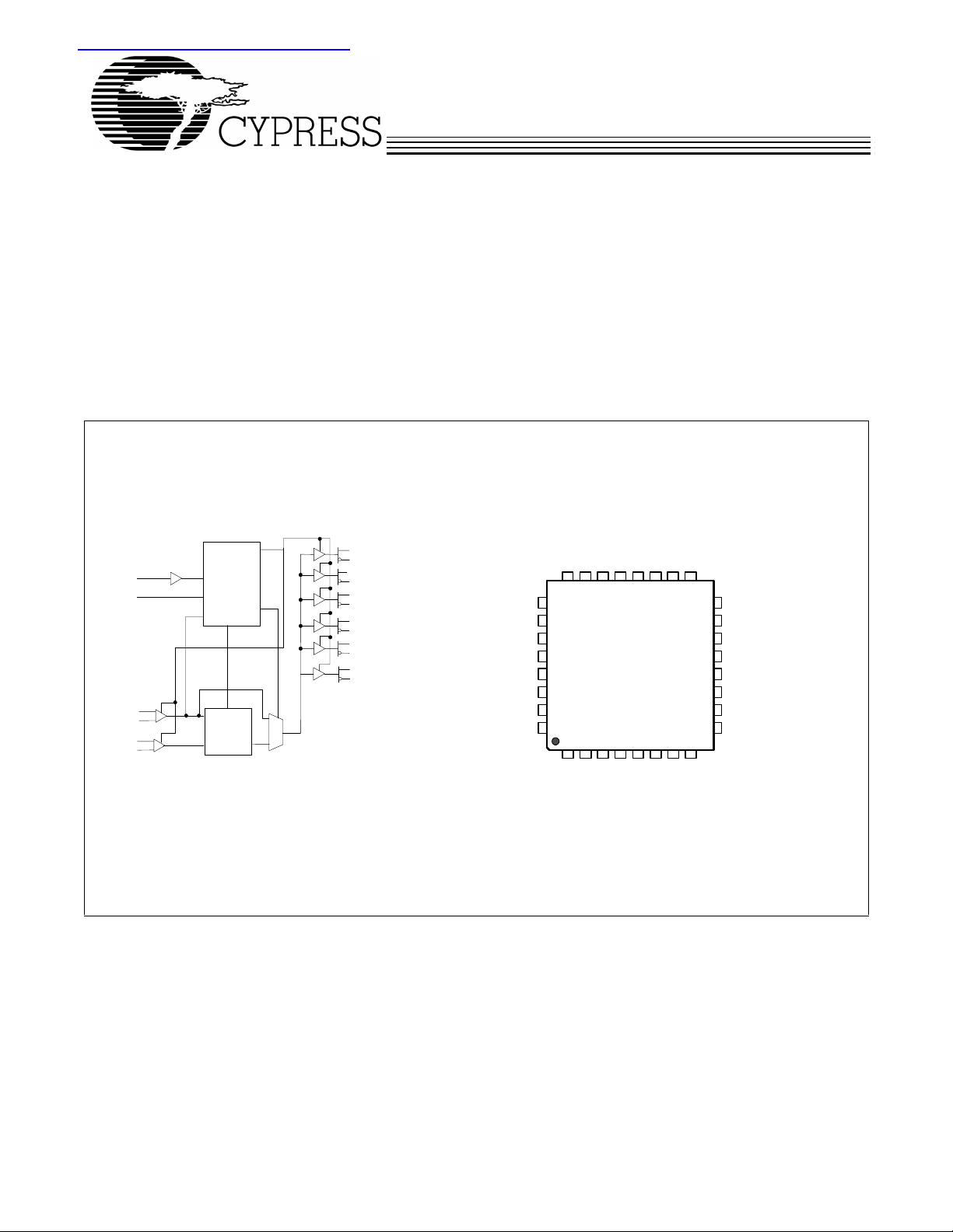
Block Diagram
2
Y0
1
Y0#
12
OE
AVDD
CLK
CLK#
FBIN
FBI
#
N
23
8
5
6
21
22
Test and
Powerdown
Logic
PLL
11
15
16
27
28
30
31
18
19
Y1
Y1#
Y2
Y2#
Y3
Y3#
Y4
Y4#
FBOUT
FBOUT#
Description
The CY2SSTV8575 is a high-p erformance, low-skew , low jitt er
zero-delay buffer designed to distribute differential clocks in
high-speed applications. The CY2SSTV8575 generates five
differential pair clock outputs from one differential pair clock
input. In addition, the CY2SSTV8575 features differential
feedback clock outputs and inputs. This allows the
CY2SSTV8575 to be used as a zero-delay buffer.
When used as a zero-delay buffer in nested clock trees, the
CY2SSTV8575 locks onto the input reference and translates
with near zero delay to low-skew outputs.
Pin Configuration
FBIN
FBIN#
TQFP-32
VDDQ
VDDQ
VDDQ
CK
OE
JEDEC MS-026 C
Y0
FBOUT#
CK#
FBOUT
VDDQ
VSS
AVDD
Y2#
Y2
VSS
VDDQ
Y1
Y1#
VSS
9 10 11 12 13 14 15 16
AVSS
VSS
VDDQ
Y3
Y3#
VDDQ
Y4
Y4#
VSS
VSS
24 23 22 21 20 19 18 17
25
26
CY2SSTV8575
29 28 27
30
32 31
12345678
Y0#
Cypress Semiconductor Corporation • 3901 North First Street • San Jose • CA 95134 • 408-943-2600
Document #: 38-07458 Rev. ** Revised October 30, 2002
CY2SSTV8575
Pin Description
Pin Name I/O Type Description
5,6 CLK, CLK# I L V Dif fere nti al Inpu t Differential Clock Input
21 FBIN# I Differential Input Feedback Clock Input. Connect to FBOUT# for accessing the
22 FBIN I Feedback Clock Input. Connec t to FBO UT for acces sing th e
2,12,15,27,30 Y(0:4) O Differential Outputs Clock + Outputs
1,11,16,28,31 Y(0:4)# O Clock – Outputs
18 FBOUT O Differential Outputs Feedback Clock Output. Connect to FBIN for normal
19 FBOUT# O Feedback Clock Output. Connect to FBIN# for normal
23 OE I Output Enable Input. When OE is set HIGH, all Q and Q#
3,4,7,13,20,26,29VDDQ 2.5V Nominal 2.5V Power Supply for Output Clock Buffers
PLL.
PLL.
operation. A bypass delay capacitor at this output will control
Input Reference/Output Clocks phase relationships.
operation. A bypass delay capacitor at this output will control
Input Reference/Output Clocks phase relationships.
outputs are enabl ed and switch at the s ame frequency as CLK.
When set LOW, all Q and Q# outpu ts are disabled (Hi-Z) and
the PLL is powered down.
8AVDD2.5V Nominal2.5V Power Supply for PLL. When AVDD is at GND, PLL is
10,14,17,24,25,32VSS 0.0V Ground Common Ground
9 AVSS 0.0V Analog Ground Analog Ground
Table 1. Function Table
INPUTS OUTPUTS PLL
AVDD OE CLK CLK# Y Y# FBOUT FBOUT#
GND H L H L H L H BYPASSED/OFF
GND H H L H L H L BYPASSED/OFF
XLLHZZZZ Off
XLHLZZZZ OFF
2.5V H L H L H L H On
2.5V H H L H L H L On
2.5V H < 20 MHz < 20 MHz Hi-Z Hi-Z Hi-Z HI-Z Off
bypassed and CLK is buffered directly to the device outputs.
During disable (OE = 0), the PLL is powered down.
Document #: 38-07458 Rev. ** Page 2 of 8
CY2SSTV8575
Power Management Functions
Output enable/disab le control of the CY2SSTV8575 allows the
user to implement power management schemes into the design. Outp uts are thre e-stated /dis abled w hen OE is as sert ed
low, see Table 1. The enabling and disabling of output s is done
in such a manner to eliminate the possibility of the partial “runt”
clocks.
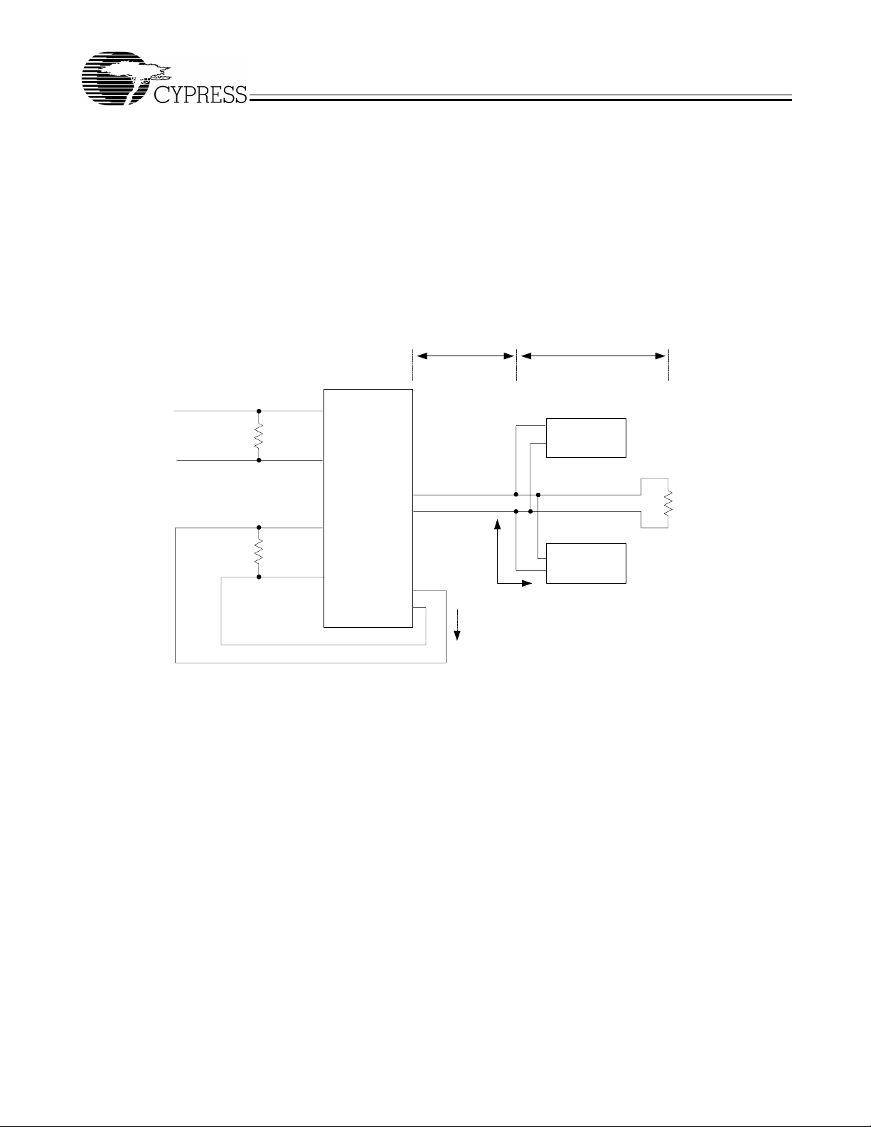
Zero Delay Buffer
When used as a zero d elay buffer th e CY2SSTV8575 will lik ely
be in a nested clock tree application. For these applications
the CY2SSTV8575 offers a differential clock input pair as a
DDR _SDRAM
represents a capacitive
load
CLK
120 Ohm
CLK#
PLL
Yx
Yx#
FBIN
PLL reference. The CY2SSTV8575 can lock onto the reference and translate with near zero delay to low-skew outputs.
For normal operation, the external feedback input, FBIN, is
connected to the feedb ac k ou tpu t, FBO U T. By connecting th e
feedback output to the feedback input the propagation delay
through the device is eliminated. The PLL works to align the
output edge with tine input reference edge thus producing a
near zero delay. The reference frequency affects the static
phase offset of the PLL and thus the relative delay between
the inputs and outputs.
When AVDD is strapped LOW, the PLL is turned off and bypassed for test purposes.
= 2.5" = 0.6" (Split to Terminator)
DDR -
SDRAM
VTR
120 Ohm
VCP
120 Ohm
FBIN#
FBOUT
FBOUT#
Figure 1. Clock Structure 1
Note:
1. Output load capacitance for 2 DDR-SDRAM loads: 5 pF < CL < 8 pF.
DDR -
SDRAM
0.3"
[1]
Document #: 38-07458 Rev. ** Page 3 of 8

DDR-SDRAM represents
a capacitive load
CLK
CLK#
120 Ohm
PLL
CY2SSTV8575
= 2.5" = 0.6" (Split to Terminator)
DDR-SDRAM
DDR-SDRAM
Stack
DDR-SDRAM
VDD
OUT
OUT#
120 Ohm
VDD
Yx
Yx#
FBIN
FBIN#
FBOUT
FBOUT#
Figure 2. Clock Structure 2
VDD/2
60 Ohm
60 Ohm
VDD/2
14 pF
14 pF
0.3"
[2]
R
DDR-SDRAM
DDR-SDRAM
VTR
= 120 Ohm
T
VCP
VTR
120 Ohm
VCP
DDR-SDRAM
Stack
Receiver
Figure 3. Differential Signal Using Direct Termination Resistor
Governing Agencies
The following agencies provide specifications that apply to the CY2SSTV8575. The agency name and relevant specification is
listed below;
Agency Name Specification
JEDEC MS - 026-C
Note:
2. Output load capacitance for 4 DDR-SDRAM loads: 10 pF < CL < 16 pF.
Document #: 38-07458 Rev. ** Page 4 of 8

CY2SSTV8575
Absolute Maximum Ratings
This device contains circuitry to protect the inputs against
damage due to high static voltages or electric field; however,
precautions should be taken to avoid application of any voltage higher than the ma ximum rated vol tages to this circ uit. For
proper operation, V
range:
< (Vin or V
V
SS
in
) < VDD (V
out
and V
Unused inputs mu st always be tied to an approp riate logic voltage level (either V
SS
or V
should be constrained to the
out
Voltage)
DDQ
).
DDQ
Parameter Description Conditions Min. Max. Unit
V
dd
V
DD
V
in
V
out
T
s
T
a
Ø
Jc
Ø
Ja
ESD
h
Supply Voltage Non Functional –0.3 3.5 VDC
Operating Voltage Functional 2.38 2.63 VDC
Input Voltage Relative to VSS –0.3 2.63 VDC
Output Voltage Relative to VSS –0.3 2.63 VDC
Temperature, Storage Non Functional –65 150 °C
Temperature, Operating Ambient Functional 0 +85 °C
Dissipation, Junction to Case Functional – 18 °C/W
Dissipation, Junction to Ambient Functional – 48 °C/W
ESD Protection (Human Body Model) – 2K Volts
FIT Failure in Time Manufacturing test – 10 ppm
DC Parameters (AV
DD
= V
= 2.5 ±5%, Temperature = 0°C to +85°C)
DDO
Parameter Description Conditions Min. Typ. Max. Unit
V
IL
V
IH
V
OL
V
OH
I
OL
I
OH
I
DDQ
I
PDS
C
in
Notes:
3. Unused inputs must be held high or low to prevent them from floating.
4. All outputs switching loaded with 16pF in 60Ω environment. See Figure 3.
Input Voltage, Low
Input Voltage, High
Output Voltage, Low V
Output Voltage, High V
Output Low Current V
Output High Current V
Dynamic Supply Current
Power Down Current OE = 0 or CLK/CLK# < 20 MHz ––100 µA.
Input pin capacitance ––4pF
[3]
[3]
OE ––0.75 V
1.75 ––V
= 2.375V, I
DDQ
= 2.375V, IOH = –12 mA 1.7 ––V
DDQ
= 2.375V, V
DDQ
= 2.375V, V
DDQ
[4]
ALL V
, FO = 170 MHz – 235 300 mA.
DDQ
= 12 mA ––0.6 V
OL
= 1.2V 26 35 – mA
OUT
= 1V 28 –32 – mA
OUT
Document #: 38-07458 Rev. ** Page 5 of 8

CY2SSTV8575
AC Input Parameters (AV
= VDDQ = 2.5 ±5%, TA = 0°C to +85°C)
DD
Parameter Description Conditions Min. Typ. Max. Unit
F
in
D
TYC
AC Output Parameters (AVDD = VDDQ = 2.5 ±5%, Temperature = 0°C to +85°C)
Input Frequency 1.25 60 – 170 MHz
Input Duty Cycle AVDD, V
= 2.5V±0.2V 40 – 60 %
DD
[5,6]
Parameter Description Conditions Min. Typ. Max. Unit
F
OR
t
LOCK
D
TYC
Output frequency range AVDD, V
Maximum PLL Lock Time AVDD, V
Duty Cycle
[7]
60 MHz to 100 MHz 49.5 50 50.5 %
= 2.5V±0.2V 60 – 170 MHz
DD
= 2.5V±0.2V ––100 µS
DD
101 MHz to 170 MHz 49 – 51 %
T
R
T
F
t
SKEW
T
PLH
T
PHL
T
ODIS
T
OENB
T
JIT(CC)
T
PHASE
T
JIT(PHASE)
Notes:
5. Parameters are guaranteed by design and characterization. Not 100% tested in production.
6. PLL is capable of meeting the specified parameters while supporting SSC synthesizers with modulation frequency between 30 kHz and 50 kHz with a down
spread of –0.5%.
7. While the pulse skew is almost constant over frequency, the duty cycle error increases at higher frequencies. This is due to the formula: duty cycle = t
where the cycle time (t
8. Refers to transition of non-inverting output.
9. All differential input and output terminals are terminated with 120Ω/16 pF as shown in Figure 2.
Rise Time 20% to 80% of V
Fall Time 20% to 80% of V
Any Output to Any Output Skew
[9]
All outputs equally loaded ––100 ps
OD
OD
Propagation Delay (Low to High) CLK to Y 1.5 3.5 6 ns
Propagation Delay (High to Low) CLK to Y 1.5 3.5 6 ns
[8]
[8]
All outputs – 3 – ns
All outputs – 3 – ns
Output Disa ble Time
Output Enable Time
Cycle to Cycle Jitter All outputs @ 66 MHz –100 ––100 ps
Phase Error –150 – 150 ps
Phase Error Jitter All outputs @ 66 MHz –50 – 50 ps
) decreas es as the frequency goes up.
C
1 – 2V/ns
1 – 2V/ns
WH/tC
,
Document #: 38-07458 Rev. ** Page 6 of 8

CY2SSTV8575
Ordering Information
Part Number Package Type Product Flow
CY2SSTV8575AC 32-pin TQFP Commercial, 0° to 85°C
CY2SSTV8575ACT 32-pin TQFP -Tape & Reel Commercial, 0° to 85°C
Package Drawing and Dimension
32-Lead Thin Plastic Quad Flatpack 7 x 7 x 1.0 mm A32
51-85063-*B
All product and company names mentioned in this document may be the trademarks of their respective owners.
Document #: 38-07458 Rev. ** Page 7 of 8
© Cypress Semiconductor Corporation, 2002. The information contained herein is subject to change without notice. Cypress Semiconductor Corporation assumes no responsibility for the use
of any circuitry other than ci rcuitry embod ied in a Cypress S emiconductor pr oduct. Nor does it convey or imply any licen se under patent or other rights. Cypress Semiconductor does not authorize
its products for use as critical components in life-support systems where a malfunction or failure may reasonably be expected to result in significant injury to the user. The inclusion of Cypress
Semiconductor products in life-support systems application implies that the manufacturer assumes all risk of such use and in doing so indemnifies Cypress Semiconductor against all charges.

Document History Page
Document Title: CY2SSTV8575 Differential Clock Buffer/Driver
Document #: 38-07458
CY2SSTV8575
Rev. ECN No.
** 120711 10/31/02 RGL New Data Sheet
Issue
Date
Orig. of
Change Description of Change
Document #: 38-07458 Rev. ** Page 8 of 8

 Loading...