

r
查询CY2LL843ZI供应商
PRELIMINARY
Features
• Operating frequency: DC to 500 MHz
• Supports DDRII SDRAM
• Two operations modes: 25 bit (1:1) and 14 bit (1:2)
• 1.8V operation
• Fully JEDEC-compliant (JESD82-7A)
• 96-ball FBGA
Functional Description
All clock and data inputs are compatible with the JEDEC
standard for SSTL_18. The control inputs are LVCMOS. All
outputs are 1.8V CMOS drivers that have been optimized to
drive the DDR-II DIMM load. The CY2SSTU32864 operates
from a differential clock (CK and CK#). Data are registered at
the crossing of CK going high, and CK# going low.
The C0 input controls the pinout configuration of the 1:2 pinout
from A configuration (when low) to B configuration (when
high). The C1 input controls the pinout configuration from
25-bit 1:1 (when low) to 14-bit 1:2 (when high). C0 = 1 and
C1 = 0 is not allowed and it will default to the C0 = C1 = 0 state.
CY2SSTU32864
1.8V, 25-bit (1:1) or 14-bit (1:2)
JEDEC-Compliant Data Registe
The device monitors both DCS# and CSR# inputs and will gate
the Qn outputs from changing states when both DCS# and
CSR# inputs are high. If either DCS# or CSR# input is low, the
Qn outputs will function normally. The RESET input has priority
over the DCS# and CSR# control and will force the outputs
low. If the DCS#-control functionality is not desired, the CSR#
input can be hardwired to ground, in which case the set-up
time requirement for DCS# would be the same as for the other
D data inputs.
The device supports low-power standby operation. When the
reset input (RESET#) is low, the differential input receivers are
disabled, and undriven (floating) data, clock, and reference
voltage (VREF) inputs are allowed. In addition, when RESET#
is low, all registers are reset and all outputs are forced low. The
LVCMOS RESET# and Cn inputs must always be held at a
valid logic high or low level. To ensure defined outputs from the
register before a stable clock has been supplied, RESET#
must be held in the low state during power-up.
In the DDR-II RDIMM application, RESET# is specified to be
completely asynchronous with respect to CK and CK#.
Therefore, no timing relationship can be guaranteed between
the two. When entering reset, the register will be cleared and
the outputs will be driven low quickly, relative to the time to
disable the differential input receivers. However, when coming
out of reset, the register will become active quickly, relative to
the time to enable the differential input receivers.
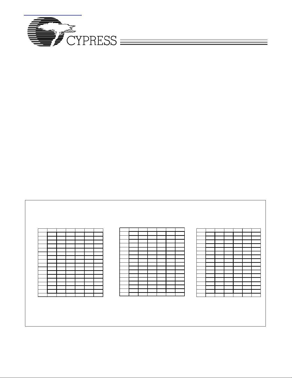
123456
A DCKE NC VREF VDD QCKE NC
B D2 D15 GND GND Q2 Q15
CD3D16VDDVDDQ3Q16
D DODT NC GND GND QODT NC
ED5D17VDDVDDQ5Q17
F D6 D1 8 GND GND Q6 Q1 8
GNCRST#VDDVDDC1C0
H CK DCS# GND GND QCS# NC
J CK# CSR# VDD VDD ZOH ZOL
K D8 D19 GND GND Q8 Q19
LD9D20VDDVDDQ9Q20
M D10 D21 GND GND Q10 Q21
N D11 D22 VDD VDD Q11 Q22
P D12 D23 GND GND Q1 2 Q2 3
R D13 D24 VDD VDD Q13 Q24
T D14 D25 VREF VDD Q14 Q25
123456
1:1 Register C0 = 0, C1 = 0
Pin Configurations
123456
A DCKE NC VREF VDD QCK EA QCKEB
B D2 NC GND GND Q2A Q2B
CD3NCVDDVDDQ3AQ3B
D DODT NC GND GND QODT A QODTB
ED5NCVDDVDDQ5AQ5B
F D6 NC GND GND Q6A Q6 B
G NC RST# VDD VDD C1 C0
H CK DCS# GND GND QCSA# QCSB#
J CK# CSR# VDD VDD ZOH ZOL
K D8 NC GND GND Q8A Q8B
LD9NCVDDVDDQ9AQ9B
M D10 NC GND GND Q10A Q10B
N D11 NC VDD VDD Q11A Q11B
P D12 NC GND GND Q12A Q12B
R D13 NC VDD VDD Q13A Q13B
T D14 NC VREF VDD Q14A Q14B
123456
1:2 Register A C0 = 0, C1 = 1
123456
AD1NCVREFVDDQ1AQ1B
BD2NCGNDGNDQ2AQ2B
CD3NCVDDVDDQ3AQ3B
DD4NCGNDGNDQ4AQ4B
ED5NCVDDVDDQ5AQ5B
FD6NCGNDGNDQ6AQ6B
G NC RST# VDD VDD C1 C0
H CK DCS# GND GND QCSA# QCSB#
J CK# CSR# VDD VDD Z OH ZOL
KD8NCGNDGNDQ8AQ8B
LD9NCVDDVDDQ9AQ9B
M D10 NC GND GND Q10A Q10B
N DODT NC VDD V DD QODTA QODT B
P D12 NC GND GND Q12A Q12B
R D13 NC VDD VDD Q13A Q13B
T DCKE NC VREF VDD QCKEA QCKEB
123456
1:2 Register B C0 = 1, C1 = 1
Cypress Semiconductor Corporation • 3901 North First Street • San Jose, CA 95134 • 408-943-2600
Document #: 38-07576 Rev. *D Revised March 29, 2005
PRELIMINARY
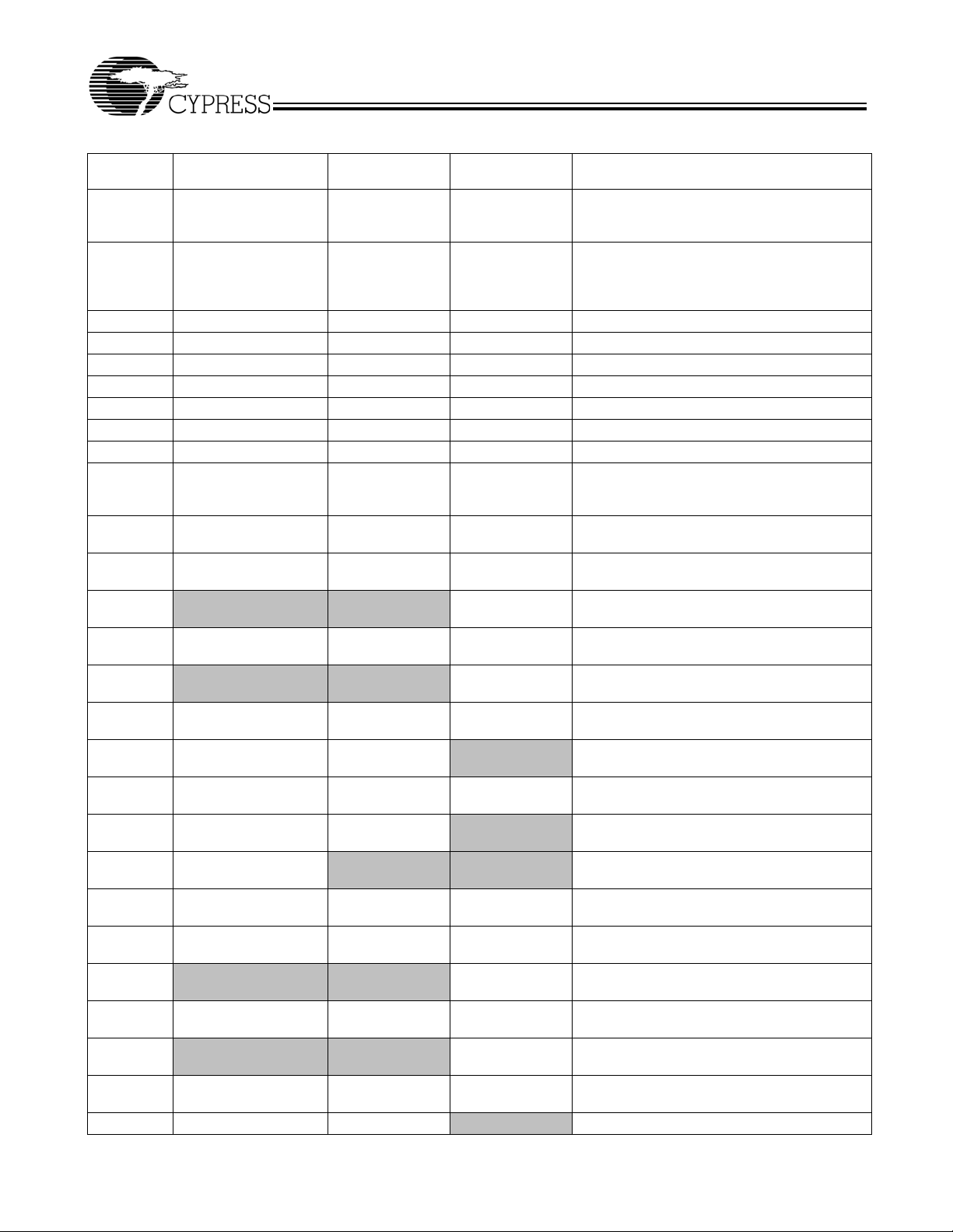
Pin Definitions
Pin Name
GND B3, B4, D3, D4, F3, F4,
VDD A4, C3, C4, E3, E4, G3,
VREF A3, T3 A3, T3 A3, T3 Input Reference Voltage
ZOHJ5 J5J5Reserved
ZOLJ6 J6J6Reserved
CK H1 H1 H1 Positive Master Clock
CK# J1 J1 J1 Negative Master Clock
C0 G6 G6 G6 Configuration Control Input
C1 G5 G5 G5 Configuration Control Input
RESET# G2 G2 G2 Asynchronous Reset – resets registers and
CSR# J2 J2 J2 Chip Select – Disables D1-D24 when both CSR#
DCS# H2 H2 H2 Chip Select – Disables D1-D24 when both CSR#
D1
D2-3 B1, C1 B1, C1 B1, C1 Data Input – clocked in on the crossing points of
D4
D5, 6, 8, 9, 10E1, F1, K1, L1, M1 E1, F1, K1, L1, M1 E1, F1, K1, L1, M1 Data Input – clocked in on the crossing points of
D11 N1 N1
D12, 13 P1, R1 P1, R1 P1, R1 Data Input – clocked in on the crossing points of
D14 T1 T1
D15-25 B2, C2, E2, F2, K2, L2,
DODT D1 D1 N1 The outputs of this register bit will not be
DCKE A1 A1 T1 The outputs of this register bit will not be
Q1A
Q2A–3A B5, C5 B5, C5 B5, C5 Data Outputs that are suspended by the DCS#
Q4A
Q5A, 6A, 8A,
9A, 10A
Q11A N5 N5
Pin Number
(C0 = 0, C1 = 0)
H3, H4, K3, K4, M3, M4,
P3, P4
G4, J3, J4, L3, L4, N3,
N4, R3, R4, T4
M2, N2, P2, R2, T2
E5, F5, K5, L5, M5 E5, F5, K5, L5, M5 E5, F5, K5, L5, M5 Data Outputs that are suspended by the DCS#
Pin Number
(C0 = 0, C1 = 1)
B3, B4, D3, D4, F3,
F4, H3, H4, K3, K4,
M3, M4, P3, P4
A4, C3, C4, E3,
E4, G3, G4, J3, J4,
L3, L4, N3, N4, R3,
R4, T4
Pin Number
(C0 = 1, C1 = 1) Description
B3, B4, D3, D4, F3,
F4, H3, H4, K3, K4,
M3, M4, P3, P4
A4, C3, C4, E3,
E4, G3, G4, J3, J4,
L3, L4, N3, N4, R3,
R4, T4
A1 Data Input – clocked in on the crossing points of
D1 Data Input – clocked in on the crossing points of
A5 Data Outputs that are suspended by the DCS#
D5 Data Outputs that are suspended by the DCS#
Ground
Power Supply Voltage
disables Vref data and clock differential input
receivers
and DCS# are High (VDD)
and DCS# are High (VDD)
CK and CK#
CK and CK#
CK and CK#
CK and CK#
Data Input – clocked in on the crossing points of
CK and CK#
CK and CK#
Data Input – clocked in on the crossing points of
CK and CK#
Data Input – clocked in on the crossing points of
CK and CK#
suspended by the DCS# and CSR# Control
suspended by the DCS# and CSR# Control
and CSR# control
and CSR# control
and CSR# control
and CSR# control
CY2SSTU32864
Document #: 38-07576 Rev. *D Page 2 of 10
PRELIMINARY
CY2SSTU32864
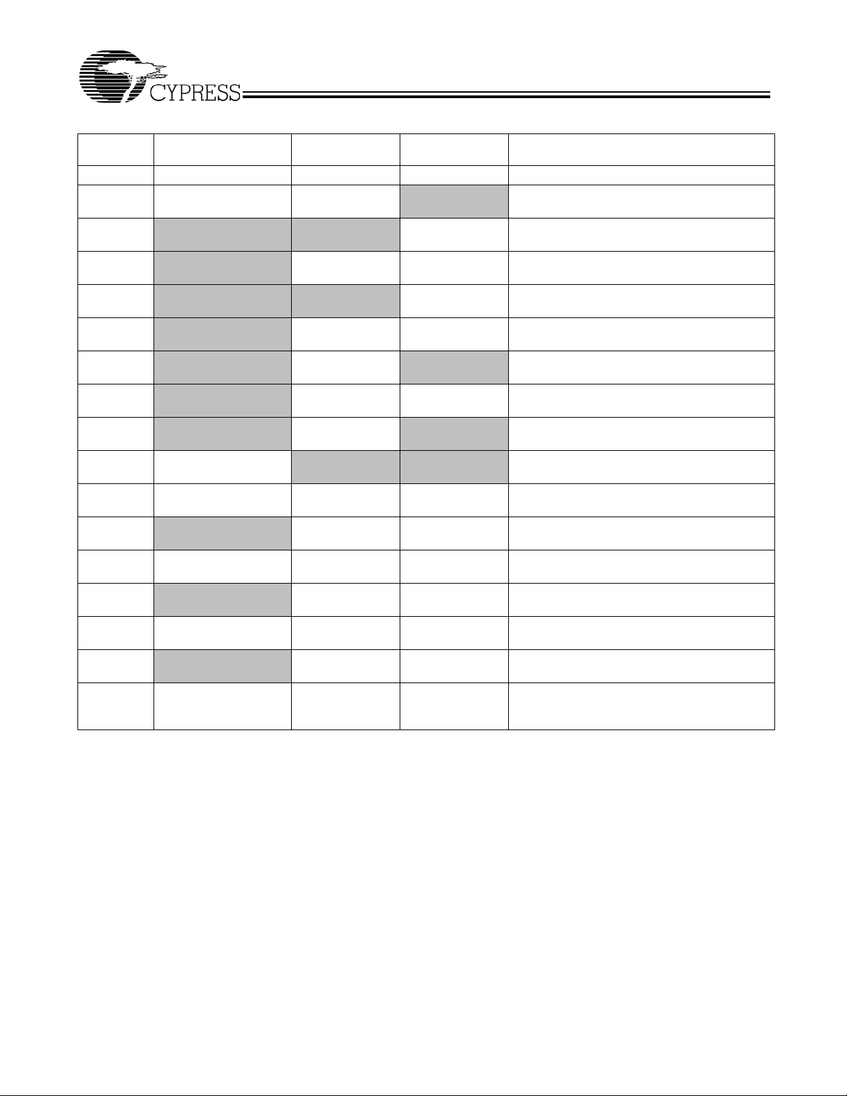
Pin Definitions (continued)
Pin Name
Q12A, Q13A P5, R5 P5, R5 P5, R5
Q14A T5 T5
Q1B
Q2B-3B
Q4B
Q5B, 6B, 8B,
9B, 10B,
Q11B
Q12B, 13B
Q14B
Q15–25 B6, C6, E6, F6, K6, L6,
QCSA# H5 H5 H5 Data outputs that will not be suspended by the
QCSB#
QODTA D5 D5 N5 Data outputs that will not be suspended by the
QODTB
QCKEA A5 A5 T5 Data outputs that will not be suspended by the
QCKEB
NC A2, A6, D2, D6, G1, H6 A2, B2, C2, D2,
Pin Number
(C0 = 0, C1 = 0)
M6, N6, P6, R6, T6
Pin Number
(C0 = 0, C1 = 1)
B6, C6 B6, C6 Data Outputs that are suspended by the DCS#
E6, F6, K6, L6, M6 E6, F6, K6, L6, M6 Data Outputs that are suspended by the DCS#
N6 Data Outputs that are suspended by the DCS#
P6, R6 P6, R6 Data Outputs that are suspended by the DCS#
T6 Data Outputs that are suspended by the DCS#
H6 H6 Data outputs that will not be suspended by the
D6 N6 Data outputs that will not be suspended by the
A6 T6 Data outputs that will not be suspended by the
E2, F2, G1, K2, L2,
M2, N2, P2, R2, T2
Pin Number
(C0 = 1, C1 = 1) Description
Data Outputs that are suspended by the DCS#
and CSR# control
A6 Data Outputs that are suspended by the DCS#
D6 Data Outputs that are suspended by the DCS#
A2, B2, C2, D2,
E2, F2, G1, K2, L2,
M2, N2, P2, R2, T2
and CSR# control
and CSR# control
and CSR# control
and CSR# control
and CSR# control
and CSR# control
and CSR# control
Data Outputs that are suspended by the DCS#
and CSR# control
DCS# and CSR# control
DCS# and CSR# control
DCS# and CSR# control
DCS# and CSR# control
DCS# and CSR# control
DCS# and CSR# control
No Connect Pins
Document #: 38-07576 Rev. *D Page 3 of 10
PRELIMINARY
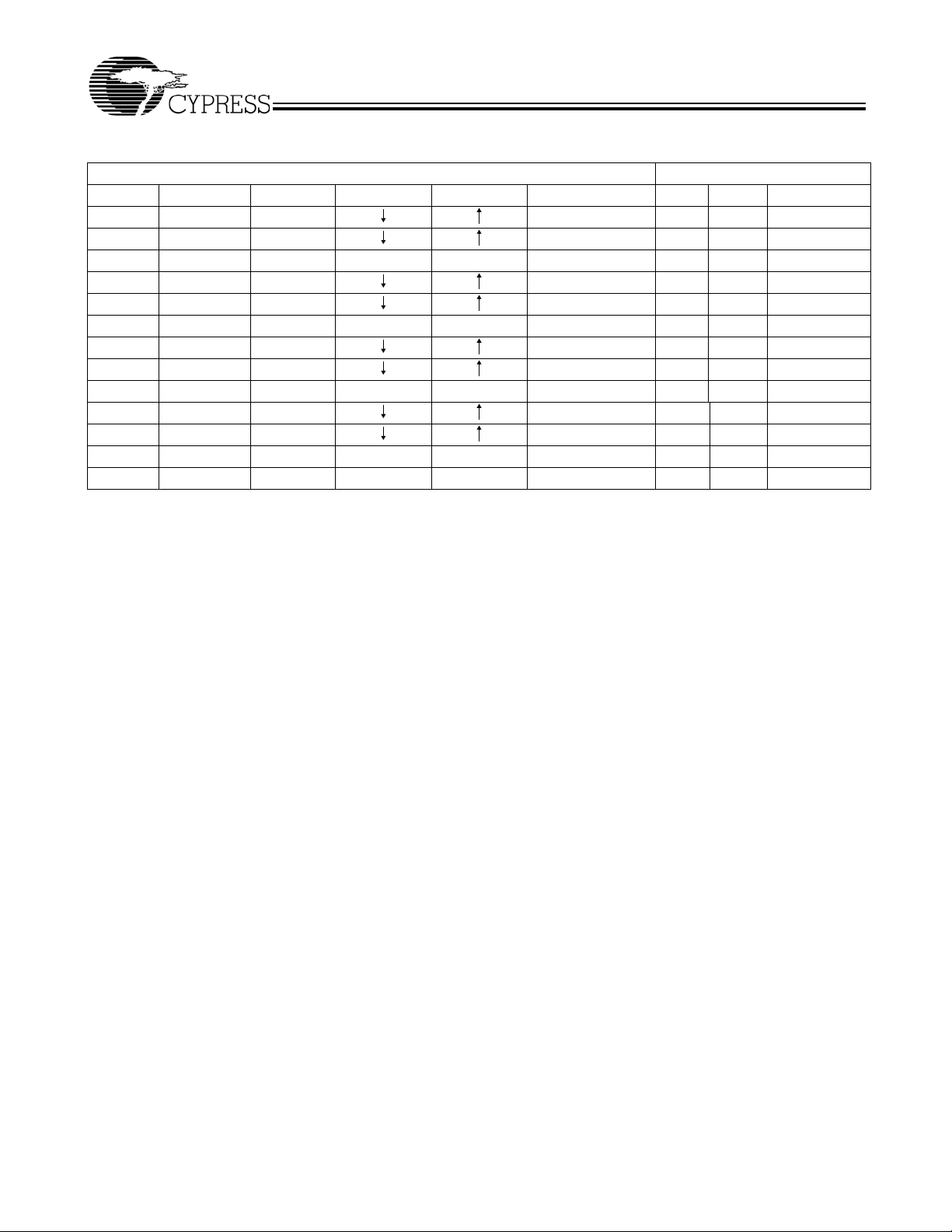
Table 1. Flip Flop Function Table
Inputs Outputs
RESET# DCS# CSR# CK CK# Dn, DODT, DCKE Qn QCS# QODT, QCKE
HL L L LLL
HL L H HLH
H L L L or H L or H X Q0 Q0 Q0
HL H L LLL
HL H H HLH
H L H L or H L or H X Q0 Q0 Q0
HH L L LHL
HH L H HHH
H H L L or H L or H X Q0 Q0 Q0
HH H L Q0HL
HH H H Q0HH
H H H L or H L or H X Q0 Q0 Q0
L X or Floating X or Floating X or Floating X or Floating X or Floating L L L
CY2SSTU32864
Document #: 38-07576 Rev. *D Page 4 of 10

PRELIMINARY
CY2SSTU32864
Absolute Maximum Conditions
[1]
Parameter Description Condition Min. Max. Unit
V
V
T
V
I
I
I
IN
OUT
S
CC
IK
OK
O
Input Voltage Range
Output Voltage Range
Storage Temperature –65 150 °C
Supply Voltage Range –0.5 2.5 V
Input Clamp Current VO < 0 or VO > V
Output Clamp Current VO < 0 or VO > V
Continuous Output Current VO = 0 to V
[2, 3]
[2, 3]
DD
DD
DD
–0.5 VDD + 0.5 V
–0.5 VDD + 0.5 V
–50 50 mA
–50 50 mA
–50 50 mA
Continuous Current through VDD/GND –100 100 mA
DC Electrical Specifications
Parameter Description Conditions Min. Max. Unit
T
A
V
DD
V
ICR
Input Differential Voltage CK, CK# 600 – mV
V
ID
V
REF
V
TT
V
I
I
I
V
IL
V
IH
VOL Output Low Voltage IOL = 100 µA, VCC = 1.7V to 1.9V – 0.2 V
V
OH
I
OH
I
OL
I
DD
Notes:
1. Stresses beyond those listed under “Absolute Maximum Ratings” may cause permanent damage to the device. These are stresses ratings only and functional
operation of the device at these or any other conditions beyond those indicated under “Recommended Operating Conditions” is not implied. Exposure to
absolute-maximum-rated conditions for extended periods may affect device reliability.
2. The input and output negative-voltage ratings may be exceeded if the input and output clamp-current ratings are observed.
3. This value is limited to 2.5V (max.)
Ambient Operating Temp 0 70 C
Operating Voltage 1.7 1.9 V
Input Differential Common
CK, CK# 0.675 1.125 V
Mode Voltage Range
Voltage Reference 0.49*V
Terminating Voltage V
REF
DD
– 40 mV V
Input Voltage 0 V
0.51*V
DD
+ 40 mV V
REF
DD
V
V
Input Current VI = VDD or GND –5 5 µA
AC Input Low Voltage Data Inputs – V
DC Input Low Voltage Data Inputs – V
AC Input High Voltage Data Inputs V
DC Input High Voltage Data Inputs V
I
= 6 mA, VCC = 1.7V – 0.5 V
OL
Output High Voltage IOH = –100 µA, VCC = 1.7V to 1.9V V
+ 250 mV – V
REF
+ 125 mV – V
REF
– 0.2 – V
DD
– 250 mV V
REF
– 125mV V
REF
IOH = –6 mA, VCC = 1.7V 1.2 – V
Output High Current – –8 mA
Output Low Current – 8 mA
Static Standby Power
RESET# = GND, IO = 0, VDD = 1.9V 100 µA
Supply Current
Static Operating Power
Supply Current
RESET# = V
IO = 0, V
DD
, VI = V
DD
= 1.9V
IH(AC)
or V
IL(AC)
,
40 mA
Document #: 38-07576 Rev. *D Page 5 of 10

PRELIMINARY
CY2SSTU32864
DC Electrical Specifications (continued)
Parameter Description Conditions Min. Max. Unit
I
DDD
C
IN
Power Supply Current
Dynamic Operating Clock
Only
Dynamic Operating per
each Data Input
RESET# = VDD, VI = V
CK# switching 50% duty cycle,
VDD = 1.8V
RESET# = VDD, VI = V
CK# switching 50% duty cycle,
VDD = 1.8V, 1 IO switching 1:1 configuration
RESET# = VDD, VI = V
CK# switching 50% duty cycle,
VDD = 1.8V, 1 IO switching 1:2 configuration
Low Power Active Mode,
CLK only
Low Power Active Mode
per each Data Input
RESET# = V
CK# switching 50% duty cycle,
V
DD
RESET# = V
CK# switching 50% duty cycle,
V
DD
CS Enabled
RESET# = V
CK# switching 50% duty cycle,
V
DD
CS Enabled
Ci (Data) VI = V
Ci (CK and CK#) V
Ci (RESET#) V
= 0.9V, VID = 600 mV 2 3 pF
IX
= VDD or GND 2.5 pF
I
, VI = V
DD
IH(AC)
IH(AC)
IH(AC)
IH(AC)
or V
or V
or V
or V
IL(AC)
IL(AC)
IL(AC)
IL(AC)
, CK,
, CK,
, CK,
, CK,
28 (typical) µA/MHz
18 (typical) µA/MHz
36 (typical) µA/MHz
27 (typical) µA/MHz
= 1.8V, CS Enabled
, VI = V
DD
IH(AC)
or V
IL(AC)
, CK,
2 (typical) µA/MHz
= 1.8V, 1 IO switching 1:1 configuration,
, VI = V
DD
IH(AC)
or V
IL(AC)
, CK,
2 (typical) µA/MHz
= 1.8V, 1 IO switching 1:2 configuration;
± 250 mV 2.5 3.5 pF
REF
AC Timing Specifications
Parameter Description Conditions Min. Max. Unit
F
CLK
T
W
[4,5]
T
ACT
[4,5]
T
INACT
T
SU
T
H
T
PDM
T
PDMS
T
rPHL
S
LR
dv/dt ∆ Delta between Rising/Falling Rates – 1 V/ns
Notes:
4. Data and V
5. Data, V
REF
and clock inputs must be held at valid levels (not floating) a minimum time of T
REF
Clock Frequency – 500 MHz
Pulse Duration CK,CK# H or L 1 – ns
Differential Input Active Time – 10 ns
Differential Input Inactive Time – 15 ns
Set up Time DCS# before crossing CK,CK#,
0.7 – ns
CSR = H, CK going high
DCS# before crossing CK,CK#,
0.5 – ns
CSR = L, CK going high
CSR, ODT, CKE and data
0.5 – ns
before crossing CK,CK#, CK
going high
Hold Time DCS#, CSRT#, ODT, CKE and
0.5 – ns
data after crossing CK,CK#, CK
going high
Propagation Delay without Switching From CK, CK# to Q 1.86 ns
Propagation Delay with Switching From CK, CK# to Q –
1.87 ns
simultaneous switching
Propagation Delay from High to Low RESET# Start to Q Low 3 ns
Slew Rate Rising dv/dt_r (20 to 80%) 1 4 V/ns
Slew Rate Falling dv/dt_f (20 to 80%) 1 4 V/ns
inputs must be low a minimum time of T
max, after RESET# is taken high.
ACT
max after RESET# is taken low.
INACT
Document #: 38-07576 Rev. *D Page 6 of 10

PRELIMINARY
CY2SSTU32864
DUT
CK Inputs
Test Point
RL = 100Ω
Test Point
CK
CK
Note: CL includes probe and jig capacitance
Figure 1. Test Load for Timing Measurements #1
DUT
OUT
Figure 2. Slew Rate Measurement Load High to Low
DUT
OUT
OUT
T
= 350ps, 50Ω
L
CL = 10pF
CL = 30pF
CL = 10pF
VDD
R
Test Point
Test Point
= 50Ω
L
VDD
R
Test Point
RL = 1000Ω
= 1000Ω
L
Figure 3. Slew Rate Measurement Load Low to High
RESET
Input
VDD/2
D
t
inact
t
act
VDD/2
50%
Figure 4. Active and Inactive Times
t
w
Input
V
ICR
V
ICR
VID
Figure 5. Pulse Duration
Document #: 38-07576 Rev. *D Page 7 of 10

PRELIMINARY
CY2SSTU32864
CK
Out pu t
RESET#
CK
CK
CK
Input
Output
V
ICR
t
su
V
REF
t
h
V
REF
Figure 6. Set-up and Hold Times
V
ICR
t
PLH
V
TT
V
ICR
t
Figure 7. Propagation Delay
VDD/2
t
RPHL
V
TT
VID
VIH
VIL
VID
PHL
VOH
V
TT
VOL
VIH
VIL
VOH
VOL
Figure 8. Propagation Delay after RESET#
Ordering Information
Part Number Package Type Product Flow
CY2SSTU32864BFXC 96-pin FBGA Commercial, 0° to 85°C
CY2SSTU32864BFXCT 96-pin FBGA– Tape and Reel Commercial, 0° to 85°C
Document #: 38-07576 Rev. *D Page 8 of 10

Package Drawing and Dimensions
PRELIMINARY
CY2SSTU32864
A1 CORNER
0.25 C
13.50±0.10
A
0.53±0.05
0.26
96 FBGA (5.5 x 13.5 x 1.2 mm) BA96A
TOP VIEW
465231
A
B
C
D
E
F
G
H
J
K
L
M
N
P
R
T
5.50±0.10
B
13.50±0.10
A
12.00
0.80
BOTTOM VIEW
65
6.00
234
1
E
G
N
R
2.00
0.80
4.00
Ø0.05 M C
Ø0.25 M C A B
Ø0.50±0.05(96X)
A1 CORNER
A
B
C
D
F
H
J
K
L
M
P
T
DIMENSIONS IN MILLIMETERS
REFERENCE JEDEC MO-205
PKG. WEIGHT: 0.23 gms
PART #
BF96A STANDARD PKG.
BP96A LEAD FREE PKG.
51-85202-*B
0.15 C
0.40±0.05
SEATING PLANE
C
0.15(4X)
B
5.50±0.10
1.20 MAX
All product and company names mentioned in this document are trademarks of their respective holders.
Document #: 38-07576 Rev. *D Page 9 of 10
© Cypress Semiconductor Corporation, 2005. The information contained herein is subject to change without notice. Cypress Semiconductor Corporation assumes no responsibility for the use
of any circuitry other than circuitry embodied in a Cypress product. Nor does it convey or imply any license under patent or other rights. Cypress products are not warranted nor intended to be
used for medical, life support, life saving, critical control or safety applications, unless pursuant to an express written agreement with Cypress. Furthermore, Cypress does not authorize its
products for use as critical components in life-support systems where a malfunction or failure may reasonably be expected to result in significant injury to the user. The inclusion of Cypress
products in life-support systems application implies that the manufacturer assumes all risk of such use and in doing so indemnifies Cypress against all charges.

PRELIMINARY
CY2SSTU32864
Document History Page
Document Title: CY2SSTU32864 1.8V, 25-bit (1:1) or 14-bit (1:2) JEDEC-Compliant Data Register
Document Number: 38-07576
Rev. ECN No. Issue Date
** 129199 09/09/03 RGL New data sheet
*A 224102 See ECN RGL Added more information to complete the data sheet
*B 269293 See ECN RGL Removed Industrial Temp.
*C 326621 See ECN RGL Data sheet re-write
*D 341657 See ECN RGL Minor Change: Corrected the lead-free coding in the Ordering table
Orig. of
Change Description of Change
Added slew rate test loads
Document #: 38-07576 Rev. *D Page 10 of 10

 Loading...