

查询CY28RS400供应商
CY28RS400
Clock Generator for ATI RS400 Chipset
Features
• Supports Intel CPU
• Selectable CPU frequencies
• Differential CPU clock pairs
• 100-MHz differential SRC clocks
• 48-MHz USB clock
• 33-MHz PCI clock
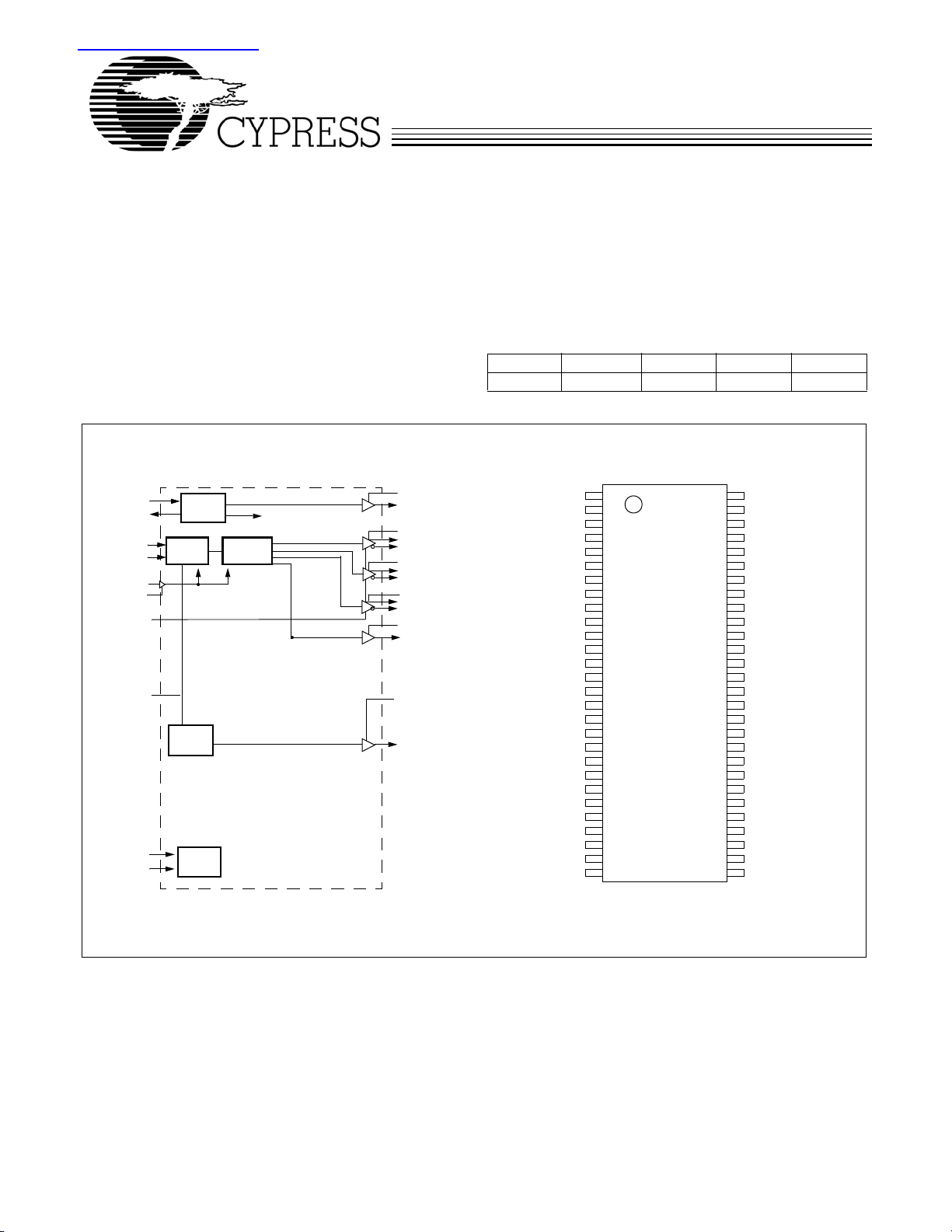
Block Diagram
XOUT
CPU_STP#
CLKREQ[0:1]#
FS_[C:A]
VTT_PWRGD#
IREF
SDATA
SCLK
XIN
PD
PLL1
PLL2
Logic
XTAL
OSC
I2C
PLL Ref Freq
Divider
Network
VDD_REF
REF[0:2]
VDD_CPU
CPUT[0:2], CPUC[0:2],
VDD_SRC
SRCT[0:5],SRCC[0:5]
VDD_SRCS
SRCST[0:1],SRCSC[0:1]
VDD_PCI
PCI
VDD_48 MHz
USB_48
VTT_PWRGD#/PD
• Low-voltage frequency select input
2
•I
C support with readback capabilities
• Ideal Lexmark Spread Spectrum profile for maximum
electromagnetic interference (EMI) reduction
• 3.3V power supply
• 56-pin SSOP and TSSOP packages
CPU SRC PCI REF USB_48
x3 x8 x1 x 3 x 1
Pin Configuration
Xin
XOUT
VDD_48
USB_48
VSS_48
SCLK
SDATA
FSC
CLKREQ#0
CLKREQ#1
SRCT5
SRCC5
VDD_SRC
VSS_SRC
SRCT4
SRCC4
SRCT3
SRCC3
VSS_SRC
VDD_SRC
SRCT2
SRCC2
SRCT1
SRCC1
VSS_SRC
SRCST1
SRCSC1
1
2
3
4
5
6
7
8
9
10
11
12
13
14
15
16
17
18
19
20
21
22
23
24
25
26
27
28
CY28RS400
56
55
54
53
52
51
50
49
48
47
46
45
44
43
42
41
40
39
38
37
36
35
34
33
32
31
30
29
VDD_REF
VSS_REF
REF0/FSA
REF1/FSB
REF2
VDD_PCI
PCI0/409_410
VSS_PCI
CPU_STOP#
CPUT0
CPUC0
VDD_CPU
VSS_CPU
CPUT1
CPUC1
CPUT2
CPUC2
VDDA
VSSA
IREF
VSS_SRC1
VDD_SRC1
SRCT0
SRCC0
VDD_SRCS
VSS_SRCS
SRCST0
SRCSC0
56 SSOP/TSSOP
Cypress Semiconductor Corporation • 3901 North First Street • San Jose, CA 95134 • 408-943-2600
Document #: 38-07637 Rev. *B Revised October 19, 2004
CY28RS400
Pin Description
Pin No. Name Type Description
47,46,43,42,
41,40
50 PCI0/409_410 I/O,PD33-MHz clock output/CPU Frequency table Select
37 IREF I A precision resistor attached to this pin is connected to the internal current reference.
54 REF0/ FSA I/O, SE, 14.318MHz REF clock ouput/ CPU Frequency Select. Intel
53 REF1/FSB I/O, SE 14.318MHz REF clock ouput
52 REF2 O, SE 14.318MHz REF clock ouput. Intel Type-5 buffer.
7 SCLK I,PU SMBus-compatible SCLOCK.This pin has an internal pullup, but is tri-stated in power-down.
8 SDATA I/O, PU SMBus compatible SDATA.This pin has an internal pullup, but is tri-stated in power-down.
27, 28, 30, 29 SRCST/C[1:0] O, DIF Differential Selectable Serial reference clock. Intel Type-X buffer. Includes overclock
12, 13, 16,
17, 18, 19,
22, 23, 24, 25
,34,33
10,11 CLKREQ#[0:1] I, SE, PDOutput Enable control for SRCT/C. Output enable control required by Minicard
4 USB_48 O, SE 48-MHz clock output. Intel Type-3A buffer.
6 VTT_PWRGD#/PD IPD3.3V LVTTL input. This pin is a level sensitive strobe used to latch the FS_A, FS_B,
48 CPU_STP# I, PU 3.3V LVTTL input. This pin is used to gate the CPU outputs. CPU outputs are turned
9 FSC I 3.3V LVTTL input. CPU Clock Frequency Select
3 VDD_48 PWR 3.3V power supply for USB outputs
45 VDD_CPU PWR 3.3V power supply for CPU outputs
51 VDD_PCI PWR 3.3V power supply for PCI outputs
56 VDD_REF PWR 3.3V power supply for REF outputs
14, 21 VDD_SRC PWR 3.3V power supply for SRC outputs
35 VDD_SRC1 PWR 3.3V power supply for SRC outputs
32 VDD_SRCS PWR 3.3V power supply for SRCS outputs
39 VDDA PWR 3.3V Analog Power for PLLs
5 VSS_48 GND Ground for USB outputs
44 VSS_CPU GND Ground for CPU outputs
49 VSS_PCI GND Ground for PCI outputs
55 VSS_REF GND Ground for REF outputs
15, 20, 26 VSS_SRC GND Ground for SRC outputs
36 VSS_SRC1 GND Ground for SRC outputs
31 VSS_SRCS GND Ground for SRCS outputs
38 VSSA GND Analog Ground
1 XIN I 14.318-MHz Crystal Input
2 XOUT O 14.318-MHz Crystal Output
CPUT/C[2:0] O, DIF Differential CPU clock output.
Intel Type-X buffer.
Intel Type-5 buffer.
0 = 410 frequency select table
1 = 409 frequency select table.
This has an internal pull-down
Type-5 buffer.
/ CPU Frequency Select. Intel Type-5 buffer.
support through SMBUS
SRCT/C[5:0] O, DIF 100 MHz Differential Serial reference clock. Intel Type-X buffer.
specification. These pins have an internal pull-down.
0 = Selected SRC outputs are enabled, 1 = Selected SRC outputs are disabled
FS_C and 409_410 inputs. After asserting VTT_PWRGD# (active low), this pin
becomes a realtime input for asserting power down (active high)
off two cycles after assertion of this pin
Document #: 38-07637 Rev. *B Page 2 of 19
CY28RS400
Frequency Select Pins (FS_A, FS_B, FS_C and
409_410)
Host clock frequency selection is achieved by applying the
appropriate logic levels to FS_A, FS_B, FS_C and 409_410
inputs prior to VTT_PWRGD# assertion (as seen by the clock
synthesizer). Upon VTT_PWRGD# being sampled low by the
clock chip (indicating processor VTT voltage is stable), the
clock chip samples the FS_A, FS_B, FS_C and 409_410 input
values. For all logic levels of FS_A, FS_B, FS_C and 409_410
VTT_PWRGD# employs a one-shot functionality in that once
Table 1. Frequency Select Table (FS_A FS_B FS_C) 410 mode, 409_410 = 0
FS_C FS_B FS_A CPU SRC PCIF/PCI REF0 USB
1 0 1 100 MHz 100 MHz 33 MHz 14.318 MHz 48 MHz
0 0 1 133 MHz 100 MHz 33 MHz 14.318 MHz 48 MHz
0 1 0 200 MHz 100 MHz 33 MHz 14.318 MHz 48 MHz
0 0 0 266 MHz 100 MHz 33 MHz 14.318 MHz 48 MHz
1 1 1 Reserved 100 MHz 33 MHz 14.318 MHz 48 MHz
Table 2. Frequency Select Table (FS_A FS_B) 410 mode, 409_410 = 1
FS_B FS_A CPU SRC PCIF/PCI REF0 USB
0 0 100 MHz 100 MHz 33 MHz 14.318 MHz 48 MHz
0 1 133 MHz 100 MHz 33 MHz 14.318 MHz 48 MHz
1 0 200 MHz 100 MHz 33 MHz 14.318 MHz 48 MHz
a valid low on VTT_PWRGD# has been sampled, all further
VTT_PWRGD#, FS_A, FS_B, FS_C and 409-410 transitions
will be ignored. There are 2 CPU frequency select tables. One
based on the CK409 specifications and one based on the
CK410 specifications. The table to be used is determined by
the value latched on the PCI0/409_410 pin by the
VTT_PWRGD/PD# pin. A '0' on this pin selects the 410
frequency table and a '1' on this pin selects the 409 frequency
table. In the 409 table, only the FS_A and FS_B pins influence
the frequency selection.
Serial Data Interface
To enhance the flexibility and function of the clock synthesizer,
a two-signal serial interface is provided. Through the Serial
Data Interface, various device functions, such as individual
clock output buffers, can be individually enabled or disabled.
The registers associated with the Serial Data Interface
initializes to their default setting upon power-up, and therefore
use of this interface is optional. Clock device register changes
are normally made upon system initialization, if any are
required. The interface cannot be used during system
operation for power management functions.
Table 3. Command Code Definition
Bit Description
7 0 = Block read or block write operation, 1 = Byte read or byte write operation
(6:5) Chip select address, set to ‘00’ to access device
(4:0) Byte offset for byte read or byte write operation. For block read or block write operations, these bits should be '00000'
Table 4. Block Read and Block Write Protocol
Block Write Protocol Block Read Protocol
Bit Description Bit Description
1 Start 1 Start
8:2 Slave address – 7 bits 8:2 Slave address – 7 bits
9 Write 9 Write
10 Acknowledge from slave 10 Acknowledge from slave
18:11 Command Code – 8 bits 18:11 Command Code – 8 bits
19 Acknowledge from slave 19 Acknowledge from slave
Data Protocol
The clock driver serial protocol accepts byte write, byte read,
block write, and block read operations from the controller. For
block write/read operation, the bytes must be accessed in
sequential order from lowest to highest byte (most significant
bit first) with the ability to stop after any complete byte has
been transferred. For byte write and byte read operations, the
system controller can access individually indexed bytes. The
offset of the indexed byte is encoded in the command code,
as described in Tab le 3.
The block write and block read protocol is outlined in Table 4
while Table 5 outlines the corresponding byte write and byte
read protocol. The slave receiver address is 11010010 (D2h).
Document #: 38-07637 Rev. *B Page 3 of 19
CY28RS400
Table 4. Block Read and Block Write Protocol (continued)
Block Write Protocol Block Read Protocol
Bit Description Bit Description
27:20 Byte Count – 8 bits 20 Repeat start
28 Acknowledge from slave 27:21 Slave address – 7 bits
36:29 Data byte 1 – 8 bits 28 Read = 1
37 Acknowledge from slave 29 Acknowledge from slave
45:38 Data byte 2 – 8 bits 37:30 Byte Count from slave – 8 bits
46 Acknowledge from slave 38 Acknowledge
.... Data Byte /Slave Acknowledges 46:39 Data byte 1 from slave – 8 bits
.... Data Byte N –8 bits 47 Acknowledge
.... Acknowledge from slave 55:48 Data byte 2 from slave – 8 bits
.... Stop 56 Acknowledge
.... Data bytes from slave / Acknowledge
.... Data Byte N from slave – 8 bits
.... NOT Acknowledge
Table 5. Byte Read and Byte Write Protocol
Byte Write Protocol Byte Read Protocol
Bit Description Bit Description
1Start 1Start
8:2 Slave address – 7 bits 8:2 Slave address – 7 bits
9Write 9Write
10 Acknowledge from slave 10 Acknowledge from slave
18:11 Command Code – 8 bits 18:11 Command Code – 8 bits
19 Acknowledge from slave 19 Acknowledge from slave
27:20 Data byte – 8 bits 20 Repeated start
28 Acknowledge from slave 27:21 Slave address – 7 bits
29 Stop 28 Read
29 Acknowledge from slave
37:30 Data from slave – 8 bits
38 NOT Acknowledge
39 Stop
Document #: 38-07637 Rev. *B Page 4 of 19
Control Registers
Byte 0:Control Register 0
Bit @Pup Name Description
7 1 SRC[T/C]5 SRC[T/C]5 Output Enable
0 = Disable (Hi-Z), 1 = Enable
6 1 SRC[T/C]4 SRC[T/C]4 Output Enable
0 = Disable (Hi-Z), 1 = Enable
5 1 SRC[T/C]3 SRC[T/C]3 Output Enable
0 = Disable (Hi-Z), 1 = Enable
4 1 SRC[T/C]2 SRC[T/C]2 Output Enable
0 = Disable (Hi-Z), 1 = Enable
3 1 SRC[T/C]1 SRC[T/C]1 Output Enable
0 = Disable (Hi-Z), 1 = Enable
2 1 SRC [T/C]0 SRC[T/C]0 Output Enable
0 = Disable (Hi-Z), 1 = Enable
1 1 SRCS[T/C]1 SRCS[T/C]1 Output Enable
0 = Disable (Hi-Z), 1 = Enable
0 1 SRCS[T/C]0 SRCS[T/C]0 Output Enable
0 = Disable (Hi-Z), 1 = Enable
Byte 1: Control Register 1
Bit @Pup Name Description
7 1 REF2 REF2 Output Enable
0 = Disable, 1 = Enable
6 1 REF1 REF1 Output Enable
0 = Disable, 1 = Enable
5 1 REF0 REF0 Output Enable
0 = Disable, 1 = Enable
4 1 PCI0 PCI0 Output Enable
0 = Disable, 1 = Enable
3 1 USB_48 USB_48MHz Output Enable
0 = Disable, 1 = Enable
2 1 CPU[T/C]2 CPU[T/C]2 Output Enable
0 = Disable (Hi-Z), 1 = Enable
1 1 CPU[T/C]1 CPU[T/C]1 Output Enable
0 = Disable (Hi-Z), 1 = Enable
0 1 CPU[T/C]0 CPU[T/C]0 Output Enable
0 = Disable (Hi-Z), 1 = Enable
CY28RS400
Byte 2: Control Register 2
Bit @Pup Name Description
7 1 CPUT/C
SRCT/C
6 1 USB_48 48MHz Output Drive Strength
5 1 PCI 33MHz Output Drive Strength
4 0 Reserved Reserved
3 1 Reserved Reserved
20 CPU
SRC
1 1 Reserved Reserved
Document #: 38-07637 Rev. *B Page 5 of 19
Spread Spectrum Selection
‘0’ = -0.35%
‘1’ = -0.50%
0 = 1x, 1 = 2x
0 = 1x, 1 = 2x
CPU/SRC Spread Spectrum Enable
0 = Spread off, 1 = Spread on
Byte 2: Control Register 2 (continued)
Bit @Pup Name Description
0 1 Reserved Reserved
Byte 3: Control Register 3
Bit @Pup Name Description
7 1 CLKREQ# CLKREQ# drive mode
0 = SRC clocks driven when stopped, 1 = SRC clocks tri-state when
stopped
6 0 CPU CPU pd drive mode
0 = CPU clocks driven when power down, 1 = CPU clocks tri-state
5 1 SRC SRC pd drive mode
0 = SRC clocks driven when power down, 1 = SRC clocks tri-state
4 0 CPU CPU_STOP# drive mode
0 = CPU clocks driven , 1 = CPU clocks tri-state
3 1 CPU2 Allow control of CPU2 with CPU_STOP#
0 = CPU2 is free running, 1 = CPU2 is stopped with CPU_STOP#
2 1 CPU1 Allow control of CPU1 with CPU_STOP#
0 = CPU1 is free running, 1 = CPU1 is stopped with CPU_STOP#
1 1 CPU0 Allow control of CPU0 with CPU_STOP#
0 = CPU0 is free running, 1 = CPU0 is stopped with CPU_STOP#
0 1 Reserved Reserved
CY28RS400
Byte 4: Control Register 4
Bit @Pup Name Description
7 0 SRC[T/C]5 SRC[T/C]5 CLKREQ0 control
1 = SRC[T/C]5 stoppable by CLKREQ#0 pin
0 = SRC[T/C]5 free running
6 0 SRC[T/C]4 SRC[T/C]4 CLKREQ#0 control
5 0 SRC[T/C]3 SRC[T/C]3 CLKREQ#0 control
4 0 SRC[T/C]2 SRC[T/C]2 CLKREQ#0 control
3 0 SRC[T/C]1 SRC[T/C]1 CLKREQ#0 control
2 0 SRC[T/C]0 SRC[T/C]0 CLKREQ#0 control
1 1 Reserved Reserved
0 1 Reserved Reserved
Byte 5: Control Register 5
Bit @Pup Name Description
7 0 SRC[T/C]5 SRC[T/C]5 CLKREQ#1 control
6 0 SRC[T/C]4 SRC[T/C]4 CLKREQ#1 control
1 = SRC[T/C]4 stoppable by CLKREQ#0 pin
0 = SRC[T/C]4 free running
1 = SRC[T/C]3 stoppable by CLKREQ#0 pin
0 = SRC[T/C]3 free running
1 = SRC[T/C]2 stoppable by CLKREQ#0 pin
0 = SRC[T/C]2 free running
1 = SRC[T/C]1 stoppable by CLKREQ#0 pin
0 = SRC[T/C]1 free running
1 = SRC[T/C]1 stoppable by CLKREQ#0 pin
0 = SRC[T/C]1 free running
1 = SRC[T/C]5 stoppable by CLKREQ#1 pin
0 = SRC[T/C]5 free running
1 = SRC[T/C]4 stoppable by CLKREQ#1 pin
0 = SRC[T/C]4 free running
Document #: 38-07637 Rev. *B Page 6 of 19

CY28RS400
Byte 5: Control Register 5 (continued)
Bit @Pup Name Description
5 0 SRC[T/C]3 SRC[T/C]3 CLKREQ#1 control
4 0 SRC[T/C]2 SRC[T/C]2 CLKREQ#1 control
3 0 SRC[T/C]1 SRC[T/C]1 CLKREQ#1 control
2 0 SRC[T/C]0 SRC[T/C]0 CLKREQ#1 control
1 0 Reserved Reserved
0 0 Reserved Reserved
Byte 6: Control Register 6
Bit @Pup Name Description
7 0 TEST_SEL REF/N or Tri-state Select
6 0 TEST_MODE Test Clock Mode Entry Control
5 0 REF REF output drive strength.
4 0 Reserved Reserved
3 HW 409_410 409_410 reflects the value of the 409_410 pin sampled on power up. 0 =
2 HW FS_C FS_C Reflects the value of the FS_C pin sampled on power up. 0 = FS_C
1 HW FS_B FS_B Reflects the value of the FS_B pin sampled on power up. 0 = FS_B
0 HW FS_A FS_A Reflects the value of the FS_A pin sampled on power up. 0 = FS_A
1 = SRC[T/C]3 stoppable by CLKREQ#1 pin
0 = SRC[T/C]3 free running
1 = SRC[T/C]2 stoppable by CLKREQ#1 pin
0 = SRC[T/C]2 free running
1 = SRC[T/C]1 stoppable by CLKREQ#1 pin
0 = SRC[T/C]1 free running
1 = SRC[T/C]1 stoppable by CLKREQ#1 pin
0 = SRC[T/C]1 free running
1 = REF/N Clock, 0 = Tri-state
1 = REF/N or Tri-state mode, 0 = Normal operation
0 = Low drive, 1 = High drive.
409_410 was low during VTT_PWRGD# assertion
was low during VTT_PWRGD# assertion.
was low during VTT_PWRGD# assertion.
was low during VTT_PWRGD# assertion.
Byte 7: Vendor ID
Bit @Pup Name Description
7 0 Revision Code Bit 3
6 0 Revision Code Bit 2
5 0 Revision Code Bit 1
4 1 Revision Code Bit 0
3 1 Vendor ID Bit 3
2 0 Vendor ID Bit 2
1 0 Vendor ID Bit 1
0 0 Vendor ID Bit 0
Document #: 38-07637 Rev. *B Page 7 of 19

CY28RS400
Crystal Recommendations
The CY28RS400 requires a Parallel Resonance Crystal.
Substituting a series resonance crystal will cause the
CY28RS400 to operate at the wrong frequency and violate the
ppm specification. For most applications there is a 300-ppm
frequency shift between series and parallel crystals due to
incorrect loading.
Table 6. Crystal Recommendations
Frequency
(Fund)
Cut Loading Load Cap
14.31818 MHz AT Parallel 20 pF 0.1 mW 5 pF 0.016 pF 35 ppm 30 ppm 5 ppm
Drive
(max.)
Shunt Cap
(max.)
Motional
(max.)
Tolerance
(max.)
Stability
(max.)
Aging
(max.)
Crystal Loading
Crystal loading plays a critical role in achieving low ppm performance. To realize low ppm performance, the total capacitance
the crystal will see must be considered to calculate the appropriate capacitive loading (CL).
Figure 1. Crystal Capacitive Clarification
Calculating Load Capacitors
In addition to the standard external trim capacitors, trace
capacitance and pin capacitance must also be considered to
correctly calculate crystal loading. As mentioned previously,
the capacitance on each side of the crystal is in series with the
Clock Chip
The following diagram shows a typical crystal configuration
using the two trim capacitors. An important clarification for the
following discussion is that the trim capacitors are in series
with the crystal not parallel. It’s a common misconception that
load capacitors are in parallel with the crystal and should be
approximately equal to the load capacitance of the crystal.
This is not true.
crystal. This means the total capacitance on each side of the
crystal must be twice the specified crystal load capacitance
(CL). While the capacitance on each side of the crystal is in
series with the crystal, trim capacitors (Ce1,Ce2) should be
calculated to provide equal capacitive loading on both sides.
XTAL
Ci2
X2
Ce2
Pin
3 to 6p
Cs2
Trace
2.8pF
Trim
33pF
Cs1
Ci1
X1
Ce1
Figure 2. Crystal Loading Example
Document #: 38-07637 Rev. *B Page 8 of 19

CY28RS400
As mentioned previously, the capacitance on each side of the
crystal is in series with the crystal. This mean the total capacitance on each side of the crystal must be twice the specified
load capacitance (CL). While the capacitance on each side of
the crystal is in series with the crystal, trim capacitors
(Ce1,Ce2) should be calculated to provide equal capacitance
loading on both sides.
Use the following formulas to calculate the trim capacitor
values for Ce1 and Ce2.
Load Capacitance (each side)
Ce = 2 * CL – (Cs + Ci)
Total Capacitance (as seen by the crystal)
CLe
=
()
1
Ce1 + Cs1 + Ci1
1
+
1
Ce2 + Cs2 + Ci2
CL ...................................................Crystal load capacitance
CLe .........................................Actual loading seen by crystal
using standard value trim capacitors
Ce .....................................................External trim capacitors
Cs.............................................. Stray capacitance (terraced)
Ci ...........................................................Internal capacitance
(lead frame, bond wires etc.)
PD
CPUT, 133MHz
PD (Power-down) Clarification
The VTT_PWRGD# /PD pin is a dual function pin. During initial
power up, the pin functions as VTT_PWRGD#. Once
VTT_PWRGD# has been sampled low by the clock chip, the
pin assumes PD functionality. The PD pin is an asynchronous
active high input used to shut off all clocks cleanly prior to
shutting off power to the device. This signal is synchronized
internal to the device prior to powering down the clock synthesizer. PD is also an asynchronous input for powering up the
system. When PD is asserted high, all clocks need to be driven
to a low value and held prior to turning off the VCOs and the
crystal oscillator.
PD (Power-down) – Assertion
When PD is sampled high by two consecutive rising edges of
CPUC, all single-ended outputs will be held low on their next
high to low transition and differential clocks must held high or
Hi-Zd (depending on the state of the control register drive
mode bit) on the next diff clock# high to low transition within
four clock periods. When the SMBus PD drive mode bit corresponding to the differential (CPU, SRC, and DOT) clock output
of interest is programmed to ‘0’, the clock output are held with
“Diff clock” pin driven high at 2 x Iref, and “Diff clock#” tristate.
If the control register PD drive mode bit corresponding to the
output of interest is programmed to “1”, then both the “Diff
clock” and the “Diff clock#” are three-state. Note the example
below shows CPUT = 133 MHz and PD drive mode = ‘1’ for all
differential outputs. This diagram and description is applicable
to valid CPU frequencies 100,133,200 and 266MHz. In the
event that PD mode is desired as the initial power-on state, PD
must be asserted high in less than 10 uS after asserting
Vtt_PwrGd#.
PD Deassertion
The power-up latency is less than 1.8 ms. This is the time from
the deassertion of the PD pin or the ramping of the power
supply until the time that stable clocks are output from the
clock chip. All differential outputs stopped in a three-state
condition resulting from power down will be driven high in less
than 300 µs of PD deassertion to a voltage greater than 200
mV. After the clock chip’s internal PLL is powered up and
locked, all outputs will be enabled within a few clock cycles of
each other. Below is an example showing the relationship of
clocks coming up.
CPUC, 133MHz
SRCT 100MHz
SRCC 100MHz
USB, 48MHz
DOT96T
DOT96C
PCI, 33 MH z
REF
Figure 3. Power-down Assertion Timing Waveform
Document #: 38-07637 Rev. *B Page 9 of 19

Tsta ble
PD
CPUT, 133MHz
CPUC, 133MHz
SRCT 100MHz
SRCC 100MHz
USB, 48MHz
DOT96T
DOT96C
PCI, 33MHz
REF
<1.8nS
Tdrive_PWRDN#
<300µS, >200mV
Figure 4. Power-down Deassertion Timing Waveform
CPU_STP# Assertion
The CPU_STP# signal is an active low input used for
synchronous stopping and starting the CPU output clocks
while the rest of the clock generator continues to function.
When the CPU_STP# pin is asserted, all CPU outputs that are
set with the SMBus configuration to be stoppable via assertion
of CPU_STP# will be stopped within two–six CPU clock
periods after being sampled by two rising edges of the internal
CPUC clock. The final states of the stopped CPU signals are
CY28RS400
CPUT = HIGH and CPUC = LOW. There is no change to the
output drive current values during the stopped state. The
CPUT is driven HIGH with a current value equal to 6 x (Iref),
and the CPUC signal will be Hi-Z. When the control register
CPU_STP Hi-Z bit corresponding to the output of interest is
programmed to ‘1’, the final state of the stopped CPU clock is
low (due to external 50 ohm pull-down resistor), both CPUT
clock and CPUC clock outputs will not be driven.
CPU_STP#
CPUT
CPUC
Figure 5. CPU_STP# Assertion Waveform
CPU_STP# Deassertion
The deassertion of the CPU_STP# signal will cause all CPU
outputs that were stopped to resume normal operation in a
synchronous manner. Synchronous manner meaning that no
short or stretched clock pulses will be produce when the clock
resumes. The maximum latency from the deassertion to active
outputs is 2 - 6 CPU clock cycles.
CPU_STP#
CPUT
CPUC
CPUT Internal
CPUC Internal
Tdrive_CPU_STP#,10nS>200mV
Figure 6. CPU_STP# Deassertion Waveform
Document #: 38-07637 Rev. *B Page 10 of 19

CPU_STOP#
CPUT(Free Runni ng
CPUC(Free Running
CPUT(Stoppable)
CPUC(Stoppable)
CY28RS400
1.8mS
PD
CPU_STOP#
PD
CPUT(Free Running)
CPUC(Free Running)
CPUT(Stoppable)
CPUC(Stoppable)
Figure 7. CPU_STP#= Driven, CPU_PD = Driven
Figure 8. CPU_STP# = Hi-Z, CPU_PD = Hi-Z
CLK_REQ[0:1]# Description
The CLKREQ#[1:0] signals are active low input used for clean
stopping and starting selected SRC outputs. The outputs
controlled by CLKREQ#[1:0] are determined by the settings in
register bytes 4 and 5. The CLKREQ# signal is a de-bounced
signal in that it’s state must remain unchanged during two
consecutive rising edges of DIFC to be recognized as a valid
assertion or de-assertion. (The assertion and de-assertion of
this signal is absolutely asynchronous).
CLK_REQ[0:1]# De-assertion [Low to High transition]
The impact of deasserting the CLKREQ#[1:0] pins is all DIF
outputs that are set in the control registers to stoppable via
de-assertion of CLKREQ#[1:0] are to be stopped after their
next transition. When the control register CLKREQ# drive
mode bit is programmed to ‘0’, the final state of all stopped
1.8mS
SRC signals is SRCT clock = High and SRCC = Low. There is
to be no change to the output drive current values, SRCT will
be driven high with a current value equal 6 x Iref,. When the
control register CLKREQ# drive mode bit is programmed to
‘1’, the final state of all stopped DIF signals is low, both SRCT
clock and SRCC clock outputs will not be driven.
CLK_REQ[0:1]# Assertion [High to Low transition]
All differential outputs that were stopped are to resume normal
operation in a glitch free manner. The maximum latency from
the assertion to active outputs is between two–six SRC clock
periods (two clocks are shown) with all SRC outputs resuming
simultaneously. If the CLKREQ# drive mode bit is
programmed to ‘1’ (three-state), the all stopped SRC outputs
must be driven high within 10 ns of CLKREQ#[1:0] assertion
to a voltage greater than 200 mV.
CLKREQ#X
SRCT(free running)
SRCC(free running)
SRCT(stoppable)
SRCT(stoppable)
Figure 9. CLK_REQ#[0:1] Assertion/Deassertion Waveform
Document #: 38-07637 Rev. *B Page 11 of 19

CY28RS400
FS_A, FS_B,FS_C
VTT_PWRGD#
PWRGD_VRM
VDD Clock Gen
Clock State
Clock Outputs
Clock VCO
VDD_A = 2.0V
Power Off
S0
State 0
Off
Off
0.2-0.3mS
Delay
State 1
Wait for
VTT_PWRGD#
On
Sample Sels
State 2 State 3
Figure 10. VTT_PWRGD# Timing Diagram
S1
Delay
VTT_PWRGD# = Low
>0.25mS
S3
VDD_A = off
Normal
Operation
VTT_PWRGD# = toggle
Device is not affected,
VTT_PWRGD# is ignored
On
S2
Sample
Inputs straps
Wait for <1.8m s
Enable Outputs
Figure 11. Clock Generator Power-up/Run State Diagram
Document #: 38-07637 Rev. *B Page 12 of 19

CY28RS400
Absolute Maximum Conditions
Parameter Description Condition Min. Max. Unit
V
DD Core Supply Voltage –0.5 4.6 V
VDDA Analog Supply Voltage –0.5 4.6 V
V
IN Input Voltage Relative to VSS –0.5 VDD+0.5 VDC
TS Temperature, Storage Non Functional –65 +150 °C
T
A Temperature, Operating Ambient Functional 0 70 °C
T
J Temperature, Junction Functional – 150 °C
ESDHBM ESD Protection (Human Body Model) MIL-STD-883, Method 3015 2000 – V
Ø
JC Dissipation, Junction to Case Mil-Spec 883E Method 1012.1 – 20 °C/W
Ø
JA Dissipation, Junction to Ambient JEDEC (JESD 51) – 60 °C/W
UL-94 Flammability Rating At 1/8 in. V–0
MSL Moisture Sensitivity Level 1
Multiple Supplies: The voltage on any input or I/O pin cannot exceed the power pin during power-up. Power supply sequencing is NOT required.
DC Electrical Specifications
Parameter Description Condition Min. Max. Unit
VDD_REF,
VDD_CPU,
VDD_PCI,
VDD_SRC,
VDD_48,
V
IL_FS
V
IH_FS
VILSMBUS Input Low Voltage SDATA, SCLK – 1.0 V
V
IHSMBUS Input High Voltage SDATA, SCLK 2.2 – V
V
VIH Input High Voltage 2.0 VDD + 0.3 V
I
IL Input Leakage Current except Pull-ups or Pull downs 0<VIN<VDD –5 5 mA
V
OL Output Low Voltage IOL = 1 mA – 0.4 V
VOH Output High Voltage IOH = 1 mA 2.4 - V
I
OZ High-Impedance Output Current –10 10 uA
C
C
OUT Output Pin Capacitance 3 5 pF
L
IN Pin Inductance –7nH
V
XIH Xin High Voltage 0.7*VDD VDD V
V
XIL Xin Low Voltage 00.3*VDD V
IDD Dynamic Supply Current At max load and frequency – 450 mA
IPD
IPD
AC Electrical Specifications
Parameter Description Condition Min. Max. Unit
Crystal
T
DC
3.3V Operating Voltage 3.3V ± 5% 3.135 3.465 V
FS_A,FS_B and FS_C Input Low Voltage VSS – 0.3 0.35 V
FS_A,FS_B and FS_C Input Low Voltage 0.7 V
IL Input Low Voltage VDD V
IN Input Pin Capacitance 3 5 pF
Power Down Supply Current PD asserted, Outputs driven – 75 mA
D
Power Down Supply Current PD asserted, Outputs Hi-Z – 2 mA
T
– 0.3 0.8 V
SS
+ 0.5 V
DD
XIN Duty Cycle The device will operate reliably with
input duty cycles up to 30/70 but the
REF clock duty cycle will not be
47.5 52.5 %
within specification
Document #: 38-07637 Rev. *B Page 13 of 19

CY28RS400
AC Electrical Specifications (continued)
Parameter Description Condition Min. Max. Unit
T
PERIOD
T
/ T
R
F
T
CCJ
L
ACC
CPU at 0.7V
T
DC
T
PERIOD
T
PERIOD
T
PERIOD
T
PERIOD
T
PERIODSS
T
PERIODSS
T
PERIODSS
T
PERIODSS
T
PERIODAbs
T
PERIODAbs
T
PERIODAbs
T
PERIODAbs
T
PERI-
ODSSAbs
T
PERI-
ODSSAbs
T
PERI-
ODSSAbs
T
PERI-
ODSSAbs
T
CCJ
T
/ T
R
F
T
RFM
∆T
R
∆T
F
T
SKEW Any CPU to CPU Clock Skew Measured at crossing point Vox – 100 ps
V
HIGH
V
LOW
V
OX
V
OVS
V
UDS
V
RB
SRC
T
DC
T
PERIOD
XIN Period When XIN is driven from an external
clock source
XIN Rise and Fall Times Measured between 0.3VDD and
0.7V
DD
69.841 71.0 ns
– 10.0 ns
XIN Cycle to Cycle Jitter As an average over 1-µs duration – 500 ps
Long-term Accuracy Over 150 ms – 300 ppm
CPUT and CPUC Duty Cycle Measured at crossing point V
100-MHz CPUT and CPUC Period Measured at crossing point V
133-MHz CPUT and CPUC Period Measured at crossing point V
200-MHz CPUT and CPUC Period Measured at crossing point V
266-MHz CPUT and CPUC Period Measured at crossing point V
100-MHz CPUT and CPUC Period, SSC Measured at crossing point V
133-MHz CPUT and CPUC Period, SSC Measured at crossing point V
200-MHz CPUT and CPUC Period, SSC Measured at crossing point V
266-MHz CPUT and CPUC Period, SSC Measured at crossing point V
100-MHz CPUT and CPUC Absolute period Measured at crossing point V
133-MHz CPUT and CPUC Absolute period Measured at crossing point V
200-MHz CPUT and CPUC Absolute period Measured at crossing point V
266-MHz CPUT and CPUC Absolute period Measured at crossing point V
100-MHz CPUT and CPUC Absolute period,
Measured at crossing point V
SSC
133-MHz CPUT and CPUC Absolute period,
Measured at crossing point V
SSC
200-MHz CPUT and CPUC Absolute period,
Measured at crossing point V
SSC
266-MHz CPUT and CPUC Absolute period,
Measured at crossing point V
SSC
CPUT/C Cycle to Cycle Jitter Measured at crossing point V
CPUT and CPUC Rise and Fall Times Measured from VOL = 0.175 to
V
= 0.525V
OH
Rise/Fall Matching Determined as a fraction of
2*(T
– TF)/(TR + TF)
R
OX
OX
OX
OX
OX
OX
OX
OX
OX
OX
OX
OX
OX
OX
OX
OX
OX
OX
45 55 %
9.997001 10.00300 ns
7.497751 7.502251 ns
4.998500 5.001500 ns
3.748875 3.751125 ns
9.997001 10.05327 ns
7.497751 7.539950 ns
4.998500 5.026634 ns
3.748875 3.769975 ns
9.912001 10.08800 ns
7.412751 7.587251 ns
4.913500 5.086500 ns
3.663875 3.836125 ns
9.912001 10.13827 ns
7.412751 7.624950 ns
4.913500 5.111634 ns
3.663875 3.854975 ns
–95ps
175 700 ps
–20%
Rise Time Variation – 250 ps
Fall Time Variation – 250 ps
Voltage High Math averages Figure 13 660 850 mv
Voltage Low Math averages Figure 13 –150 – mv
Crossing Point Voltage at 0.7V Swing 250 550 mv
Maximum Overshoot Voltage
–
V
HIGH
0.3
+
Minimum Undershoot Voltage –0.3 – V
Ring Back Voltage See Figure 13. Measure SE – 0.2 V
SRCT and SRCC Duty Cycle Measured at crossing point V
100-MHz SRCT and SRCC Period Measured at crossing point V
OX
OX
45 55 %
9.997001 10.00300 ns
V
Document #: 38-07637 Rev. *B Page 14 of 19

CY28RS400
AC Electrical Specifications (continued)
Parameter Description Condition Min. Max. Unit
T
PERIODSS
T
PERIODAbs
T
PERI-
ODSSAbs
T
SKEW
T
SKEW Any SRCS clock to Any SRCS clock Skew Measured at crossing point Vox - 250 ps
T
CCJ
L
ACC
T
/ T
R
F
T
RFM
∆T
R
∆T
F
V
HIGH
V
LOW
V
OX
V
OVS
V
UDS
V
RB
PCI
T
DC
T
PERIOD
T
PERIODSS
T
PERIODAbs
T
PERI-
ODSSAbs
T
HIGH
T
LOW
T
/ T
R
F
T
CCJ
USB
T
DC
T
PERIOD
T
PERIODAbs
T
HIGH
T
LOW
T
/ T
R
F
T
CCJ
REF
T
DC
T
PERIOD
T
PERIODAbs
100-MHz SRCT and SRCC Period, SSC Measured at crossing point V
100-MHz SRCT and SRCC Absolute Period Measured at crossing point V
100-MHz SRCT and SRCC Absolute Period, SSC Measured at crossing point V
Any SRCT/C to SRCT/C Clock Skew Measured at crossing point V
SRCT/C Cycle to Cycle Jitter Measured at crossing point V
SRCT/C Long Term Accuracy Measured at crossing point V
SRCT and SRCC Rise and Fall Times Measured from VOL = 0.175 to
V
= 0.525V
OH
Rise/Fall Matching Determined as a fraction of
2*(T
– TF)/(TR + TF)
R
OX
OX
OX
OX
OX
OX
9.997001 10.05327 ns
10.12800 9.872001 ns
9.872001 10.17827 ns
– 250 ps
– 125 ps
– 300 ppm
175 700 ps
–20%
Rise TimeVariation – 125 ps
Fall Time Variation – 125 ps
Voltage High Math averages Figure 13 660 850 mv
Voltage Low Math averages Figure 13 –150 – mv
Crossing Point Voltage at 0.7V Swing 250 550 mV
Maximum Overshoot Voltage
–
V
HIGH
0.3
+
Minimum Undershoot Voltage –0.3 – V
Ring Back Voltage See Figure 13. Measure SE – 0.2 V
PCI Duty Cycle Measurement at 1.5V 45 55 %
Spread Disabled PCI Period Measurement at 1.5V 29.99100 30.00900 ns
Spread Enabled PCI Period, SSC Measurement at 1.5V 29.9910 30.15980 ns
Spread Disabled PCI Period Measurement at 1.5V 29.49100 30.50900 ns
Spread Enabled PCI Period, SSC Measurement at 1.5V
29.49100 30.65980 ns
PCI high time Measurement at 2.4V 12.0 – ns
PCI low time Measurement at 0.4V 12.0 – ns
PCI rise and fall times Measured between 0.8V and 2.0V
1.0 4.0
PCI Cycle to Cycle Jitter Measurement at 1.5V – 500 ps
Duty Cycle Measurement at 1.5V 45 55 %
Period Measurement at 1.5V 20.83125 20.83542 ns
Absolute Period Measurement at 1.5V 20.48125 21.18542 ns
USB high time Measurement at 2.4V 8.094 10.036 ns
USB low time Measurement at 0.4V 7.694 9.836 ns
Rise and Fall Times Measured between 0.8V and 2.0V
1.0 2.0
Cycle to Cycle Jitter Measurement at 1.5V – 350 ps
REF Duty Cycle Measurement at 1.5V 45 55 %
REF Period Measurement at 1.5V 69.8203 69.8622 ns
REF Absolute Period Measurement at 1.5V 68.82033 70.86224 ns
V
V/n
s
V/n
s
Document #: 38-07637 Rev. *B Page 15 of 19

CY28RS400
AC Electrical Specifications (continued)
Parameter Description Condition Min. Max. Unit
T
/ T
R
F
T
CCJ
ENABLE/DISABLE and SET-UP
T
STABLE
T
SS
T
SH
Test and Measurement Set-up
For PCI Single-ended Signals and Reference
The following diagram shows the test load configurations for
the single-ended PCI, USB, and REF output signals.
REF Rise and Fall Times Measured between 0.8V and 2.0V
0.5 4.0
REF Cycle to Cycle Jitter Measurement at 1.5V – 1000 ps
Clock Stabilization from Power-up – 1.8 ms
Stopclock Set-up Time 10.0 – ns
Stopclock Hold Time 0 – ns
Measurement
Point
5pF
Measurement
Point
5pF
PCI/
USB
12Ω
12Ω
60Ω
60Ω
V/n
s
12Ω
12Ω
REF
12Ω
Figure 12. Single-ended Load Configuration
For Differential CPU and SRC Output Signals
The following diagram shows the test load configuration for the
differential CPU and SRC outputs.
CPUT
SRCT
CPUC
SRCC
IR E F
475Ω
33Ω
33Ω
100 Ω
49.9Ω
100 Ω
49.9Ω
60Ω
60Ω
60Ω
Measurement
Point
5pF
Measurement
Point
5pF
Measurement
Point
5pF
Measurement
Point
2pF
Measurement
Point
2pF
Figure 13. 0.7V Load Configuration
Document #: 38-07637 Rev. *B Page 16 of 19

g
CY28RS400
2.4V
1.5V
0.4V
3.3V si
-
3.3V
T
R
T
DC
nals
T
F
-
0V
Figure 14. Single-ended Output Signals (for AC Parameters Measurement)
Ordering Information
Part Number Package Type Product Flow
Standard
CY28RS400OC 56-pin SSOP Commercial, 0° to 70°C
CY28RS400OCT 56-pin SSOP – Tape and Reel Commercial, 0
CY28RS400ZC 56-pin TSSOP Commercial, 0
CY28RS400ZCT 56-pin TSSOP – Tape and Reel Commercial, 0
Lead-free
CY28RS400OXC 56-pin SSOP Commercial, 0° to 70°C
CY28RS400OXCT 56-pin SSOP – Tape and Reel Commercial, 0
CY28RS400ZXC 56-pin TSSOP Commercial, 0
CY28RS400ZXCT 56-pin TSSOP – Tape and Reel Commercial, 0
° to 70°C
° to 70°C
° to 70°C
° to 70°C
° to 70°C
° to 70°C
Package Diagrams
28
29
0.088
0.092
0.025
BSC
56-Lead Shrunk Small Outline Package O56
.020
1
0.395
0.420
0.292
0.299
56
0.720
0.730
0.008
0.0135
0.008
0.016
0.095
0.110
SEATING PLANE
0.110
GAUGE PLANE
DIMENSIONS IN INCHES MIN.
.010
0°-8°
0.024
0.040
MAX.
0.005
0.010
51-85062-*C
Document #: 38-07637 Rev. *B Page 17 of 19

Package Diagrams (continued)
56-Lead Thin Shrunk Small Outline Package, Type II (6 mm x 12 mm) Z56
0.249[0.009]
28
29 56
1
5.994[0.236]
6.198[0.244]
7.950[0.313]
8.255[0.325]
CY28RS400
DIMENSIONS IN MM[INCHES] MIN.
MAX.
REFERENCE JEDEC MO-153
PACKAGE WEIGHT 0.42gms
PART #
Z5624 STANDARD PKG.
ZZ5624 LEAD FREE PKG.
13.894[0.547]
14.097[0.555]
0.851[0.033]
0.950[0.037]
Purchase of I2C components from Cypress or one of its sublicensed Associated Companies conveys a license under the Philips
2
C Patent Rights to use these components in an I2C system, provided that the system conforms to the I2C Standard Specification
I
0.500[0.020]
BSC
0.170[0.006]
0.279[0.011]
0.051[0.002]
0.152[0.006]
1.100[0.043]
MAX.
0.20[0.008]
SEATING
PLANE
GAUGE PLANE
0.25[0.010]
0°-8°
0.508[0.020]
0.762[0.030]
0.100[0.003]
0.200[0.008]
51-85060-*C
as defined by Philips. ATI is a registered trademark of ATI Technologies Inc. HyperTransport is a trademark of the HyperTransport
Technology Consortium. Intel and Pentium are registered trademarks of Intel Corporation. AMD is a registered trademark of
Advanced Micro Devices, Inc. All product and company names mentioned in this document are trademarks of their respective
holder.
Document #: 38-07637 Rev. *B Page 18 of 19
© Cypress Semiconductor Corporation, 2004. The information contained herein is subject to change without notice. Cypress Semiconductor Corporation assumes no responsibility for the use
of any circuitry other than circuitry embodied in a Cypress product. Nor does it convey or imply any license under patent or other rights. Cypress products are not warranted nor intended to be
used for medical, life support, life saving, critical control or safety applications, unless pursuant to an express written agreement with Cypress. Furthermore, Cypress does not authorize its
products for use as critical components in life-support systems where a malfunction or failure may reasonably be expected to result in significant injury to the user. The inclusion of Cypress
products in life-support systems application implies that the manufacturer assumes all risk of such use and in doing so indemnifies Cypress against all charges.

Document History Page
Document Title: CY28RS400 Clock Generator for ATI RS400 Chipset
Document Number: 38-07637
REV. ECN NO. Issue Date
** 204582 See ECN RGL New data sheet
*A 215824 See ECN RGL Minor Change: To post on the external web
*B 278494 See ECN RGL Changed pins 10 and 11 from internal Pull up to Pull down .
Orig. of
Change Description of Change
Changed polarity of CLKREQ#
Added register byte 3 bits [1:3] for CPU Stop control.
Removed all 166, 333 and 400-MHz references
Changed the USB Rise/Fall times from 1.0 to 0.5V/ns
CY28RS400
Document #: 38-07637 Rev. *B Page 19 of 19
 Loading...