

r
X
查询CY26049ZXC-22供应商
CY26049-22
FailSafe™ PacketClock™
Global Communications Clock Generato
Features
• Fully integrated phase-locked loop (PLL)
• FailSafe output
• PLL driven by a crystal oscillator that is phase aligned
with external reference
• 100-MHz output from 10-MHz input
• Low-jitter, high-accuracy outputs
• 3.3V ± 5% operation
• 16-lead TSSOP
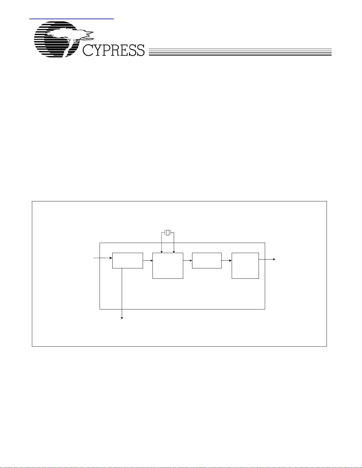
Logic Block Diagram
external pullable crystal
(10MHz)
IN
input reference
(10MHz)
ICL K
FAILSAFE
CONTROL
TM
DIGITAL
CONTROLLED
CRYSTAL
OSCILLATOR
Benefits
• Integrated high-performance PLL tailored for telecommunications frequency synthesis eliminates the need for external
loop filter components
• When reference is off, DCXO maintains clock outputs and
SAFE pin indicates FailSafe conditions
• DCXO maintains continuous operation should the input
reference clock fail
• Glitch-free transition simplifies system design
• Works with commonly available, low-cost 10-MHz crystal
• Zero-ppm error for all output frequencies
• Compatible across industry standard design platforms
• Industry standard package with 6.4 × 5.0 mm
a height profile of just 1.1 mm
XOUT
PHASE
LOCKED
LOOP
OUTPUT
DIVIDER
CLKA
100MHz
2
footprint and
SAFE
ICL K d ete cte d
Cypress Semiconductor Corporation • 3901 North First Street • San Jose, CA 95134 • 408-943-2600
Document #: 38-07730 Rev. ** Revised January 12, 2005
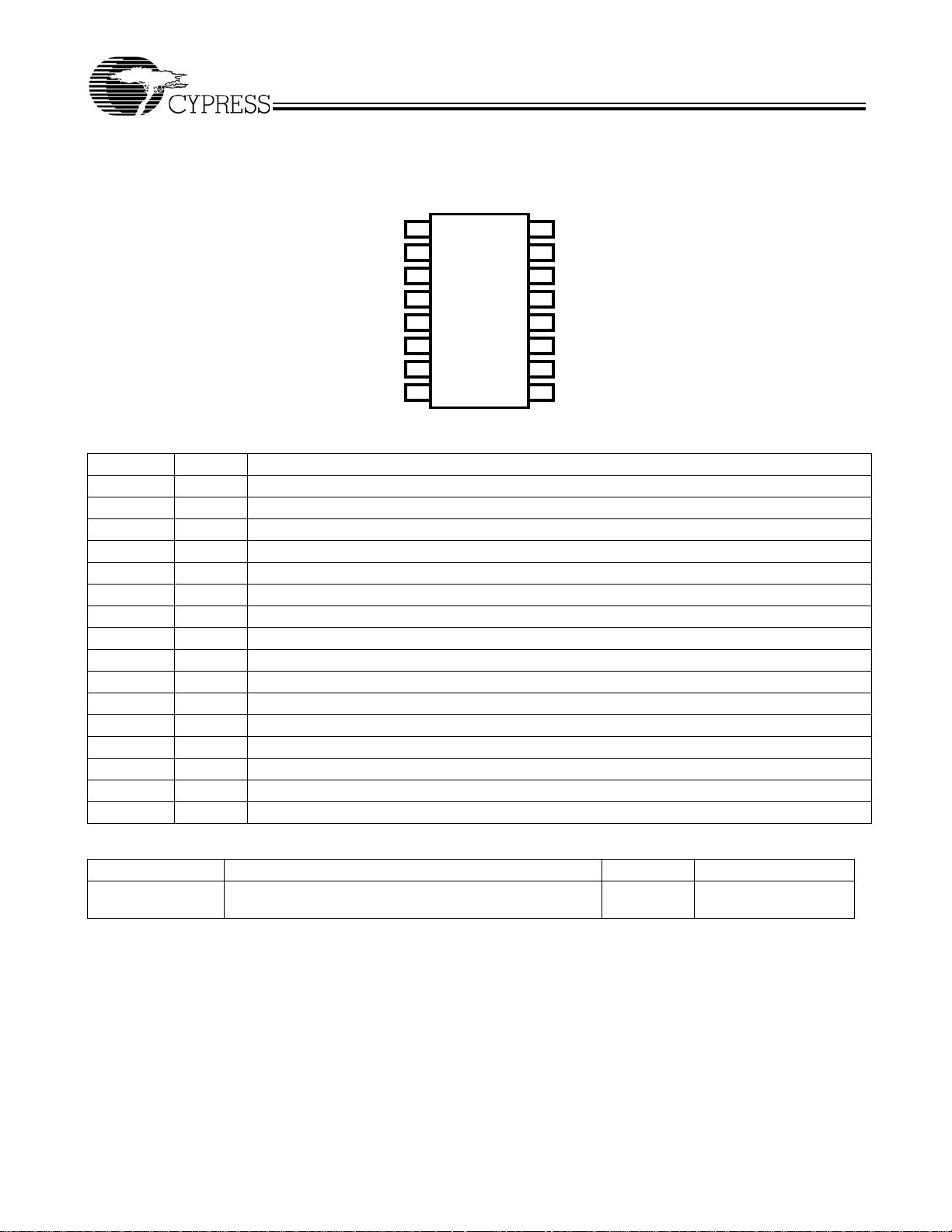
Pin Configuration
16-pin TSSOP
Top V iew
ICLK 1 16 NC
NC 2 15
NC
3 14 NC
NC 4 13 NC
VDD 5 12 VDD
VSS 6 11 VSS
NC 7 10 SAFE
XIN 8 9 XOUT
CLKA
Pin Description
Pin Number Pin Name Pin Description
1ICLKReference Input Clock; 10 MHz.
2NC No Connect.
3NCNo Connect.
4NCNo Connect.
5VDDVoltage Supply; 3.3V.
6VSSGround.
7NCNo Connect
8XINPullable Crystal Input; 10 MHz.
9XOUTPullable Crystal Output; 10 MHz.
10 SAFE High = reference ICLK within range, Low = reference ICLK out of range.
11 VS S Ground.
12 VDD Voltage Supply; 3.3V.
13 NC No Connect.
14 NC No Connect.
15 CLKA Clock Output. 100 MHz
16 NC No Connect.
CY26049-22
Selector Guide
Part Number Input Frequency Range Outputs Output Frequencies
CY26049ZXC-22 Reference Input Clock: 10 MHz
Crystal: 10-MHz pullable Crystal per Cypress Specification
Description
CY26049-22 is a FailSafe frequency synthesizer with a
reference clock input and 100-MHz output. The device
provides an optimum solution for applications where
continuous operation is required in the event of a primary clock
failure. The continuous, glitch-free operation is achieved by
using a DCXO, which serves as a primary clock source. The
FailSafe control circuit synchronizes the DCXO oscillator with
the reference as long as the reference is within the pull range
of the crystal.
Document #: 38-07730 Rev. ** Page 2 of 6
In the event of a reference clock failure the DCXO maintains
the last frequency of the reference clock. The unique feature
of the CY26049-22 is that the DCXO is, in fact, the primary
clocking source. When the reference clock is restored, the
DCXO automatically resynchronizes to the reference. The
status of the reference clock input, as detected by the
CY26049-22, is reported by the SAFE pin.
1 100 MHz

CY26049-22
Absolute Maximum Conditions
Supply Voltage (VDD) ........................................–0.5 to +7.0V
DC Input Voltage...................................... –0.5V to V
Storage Temperature (Non-Condensing) .... –55°C to +125°C
DD
+ 0.5
Data Retention @ Tj = 125°C................................ >10 Years
Package Power Dissipation...................................... 350 mW
ESD (Human Body Model) MIL-STD-883.................... 2000V
(Above which the useful life may be impaired. For user guidelines, not tested.)
Junction Temperature ................................ –40°C to +125°C
Recommended Pullable Crystal Specifications
Parameter Name Comments Min. Typ. Max. Unit
F
NOM
C
LNOM
R
1
R3/R
1
Nominal crystal frequency Parallel resonance, fundamental mode,
–10–MHz
AT cut
Nominal load capacitance – 14 – pF
Equivalent series resistance (ESR) Fundamental mode – – 25 Ω
Ratio of third overtone mode ESR to
fundamental mode ESR
Ratio used because typical R1 values
are much less than the maximum spec
3––
DL Crystal drive level No external series resistor assumed – 0.5 2 mW
F
3SEPLI
F
3SEPLO
C
0
C
0/C1
C
1
Third overtone separation from 3*F
Third overtone separation from 3*F
High side 400 – – ppm
NOM
Low side – – –200 ppm
NOM
Crystal shunt capacitance – – 7 pF
Ratio of shunt to motional capacitance 180 – 250
Crystal motional capacitance 14.4 18 21.6 fF
Recommended Operating Conditions
Parameter Description Min. Typ. Max. Unit
V
T
C
t
pu
DD
AC
LOAD
Operating Voltage 3.15 3.3 3.45 V
Ambient Temperature (Commercial Temperature) 0 – 70 °C
Max Output Load Capacitance – – 15 pF
Power-up time for all VDDs to reach minimum specified
0.05 – 500 ms
voltage (power ramps must be monotonic)
DC Electrical Specifications (Commercial Temp: 0°to 70°C)
Parameter Description Test Conditions Min. Typ. Max. Unit
I
I
V
V
I
I
C
I
OH
OL
IH
IL
IH
IL
IN
DD
Output High Current VOH = VDD – 0.5, VDD = 3.3V (source) 12 24 – mA
Output Low Current V
Input High Voltage CMOS Levels 0.7 – – V
Input High Voltage CMOS Levels – – 0.3 V
Input High Current VIH=V
= 0.5, VDD = 3.3V (sink) 12 24 – mA
OL
DD
–510µA
DD
DD
Input Low Current VIL=0V – 5 10 µA
Input Capacitance – – 7 pF
Supply Current C
= 15 pF, VDD = 3.45V – – 45 mA
LOAD
AC Electrical Specifications (Commercial Temp: 0° to 70°C)
Parameter Description Test Conditions Min. Typ. Max. Unit
f
ICLK-E
LR FailSafe
DC = t
T
PJIT1
Note:
1. Dependent on crystals chosen and crystal specs.
Document #: 38-07730 Rev. ** Page 3 of 6
Frequency, Input Clock Input Clock Frequency, External Mode – 10 – MHz
Lock Range
Output Duty Cycle Duty Cycle defined in Figure 1, measured at 50% of V
2/t1
[1]
Range of reference ICLK for Safe = High –250 – +250 ppm
45 50 55 %
DD
Clock Jitter Period Jitter, Peak to Peak, 10,000 periods – – 250 ps
RMS Period Jitter – – 50 ps

CY26049-22
V
V
A
AC Electrical Specifications (Commercial Temp: 0° to 70°C) (continued)
Parameter Description Test Conditions Min. Typ. Max. Unit
t
6
t
fs_lock
f
error
ER Rising Edge Rate Output Clock Edge Rate, Measured from 20% to 80% of
EF Falling Edge Rate Output Clock Edge Rate, Measured from 20% to 80% of
Voltage and Timing Definitions
PLL Lock Time Time for PLL to lock within ± 150 ppm of target frequency – – 3 ms
FailSafe Lock Time Time for PLL to lock to ICLK (outputs phase aligned with
––7s
ICLK and Safe = High)
Frequency Synthesis Error Actual mean frequency error vs. target – 0 – ppm
0.8 1.4 2 V/ns
V
DD
, C
= 15 pF. See Figure 2.
LOAD
0.8 1.4 2 V/ns
VDD, C
= 15 pF. See Figure 2.
LOAD
t1
t2
Test Circuit
CLK
50%
50%
Figure 1. Duty Cycle Definition; DC = t2/t1
t4
CLK
t3
80%
20%
Figure 2. Rise and Fall Time Definitions: ER = 0.6 x VDD / t3, EF = 0.6 x VDD / t4
ICLK
DD
0.1uF
1
2
3
4
5
6
7
8
16
15
14
13
12
11
10
9
CLK
C
LOAD
DD
0.1uF
10MHz
Ordering Information
Ordering Code Package Type Operating Temperature Range
Lead-Free
CY26049ZXC-22 16-lead TSSOP Commercial 0° to 70°C
CY26049ZXC-22T 16-lead TSSOP—Tape and Reel Commercial 0° to 70°C
Document #: 38-07730 Rev. ** Page 4 of 6

Package Drawing and Dimensions
16-lead TSSOP 4.40 MM Body Z16.173
CY26049-22
1
PIN1ID
DIMENSIONS IN MM[INCHES] MIN.
MAX.
REFERENCE JEDEC MO-153
0.65[0.025]
0.85[0.033]
0.95[0.037]
BSC.
4.90[0.193]
5.10[0.200]
4.30[0.169]
4.50[0.177]
16
0.19[0.007]
0.30[0.012]
0.05[0.002]
0.15[0.006]
6.25[0.246]
6.50[0.256]
1.10[0.043] MAX.
0.076[0.003]
SEATING
PLANE
PACKAGE WEIGHT 0.05gms
0.25[0.010]
BSC
GAUGE
PLANE
0°-8°
0.50[0.020]
0.70[0.027]
51-85091-*A
0.09[[0.003]
0.20[0.008]
FailSafe and PacketClock are trademarks of Cypress Semiconductor. Corporation. All product and company names mentioned
in this document are the trademarks of their respective holders.
Document #: 38-07730 Rev. ** Page 5 of 6
© Cypress Semiconductor Corporation, 2005. The information contained herein is subject to change without notice. Cypress Semiconductor Corporation assumes no responsibility for the use
of any circuitry other than circuitry embodied in a Cypress product. Nor does it convey or imply any license under patent or other rights. Cypress products are not warranted nor intended to be
used for medical, life support, life saving, critical control or safety applications, unless pursuant to an express written agreement with Cypress. Furthermore, Cypress does not authorize its
products for use as critical components in life-support systems where a malfunction or failure may reasonably be expected to result in significant injury to the user. The inclusion of Cypress
products in life-support systems application implies that the manufacturer assumes all risk of such use and in doing so indemnifies Cypress against all charges.

Document History Page
Document Title: CY26049-22 FailSafe™ PacketClock™ Global Communications Clock Generator
Document Number: 38-07730
REV. ECN No. Issue Date
** 308456 See ECN RGL New Data Sheet
Orig. of
Change Description of Change
CY26049-22
Document #: 38-07730 Rev. ** Page 6 of 6
 Loading...