

r
CY25811/12/14
Spread Spectrum Clock Generato
Features
• 4- to 32-MHz input frequency range
• 4- to 128-MHz output frequency range
• Accepts clock, crystal, and resonator inputs
• 1x, 2x, and 4x frequency multiplication:
— CY25811: 1x; CY25812: 2x; CY25814: 4x
• Center and down spread modulation
• Low power dissipation:
— 3.3V = 52 mW-typ @ 6MHz
— 3.3V = 60 mW-typ @ 12MHz
— 3.3V = 72 mW-typ @ 24MHz
• Low cycle-to cycle jitter:
— 8 MHz = 450 ps-max
— 16 MHz = 225 ps-max
— 32 MHz = 150 ps-max
• Available in 8-pin SOIC and TSSOP packages
• Commercial and industrial temperature ranges
Applications
• Printers and MFPs
• LCD panels
• Digital copiers
•PDAs
• CD-ROM, VCD, and DVD
• Networking, LAN/WAN
• Scanners
• Modems
• Embedded digital systems
Benefits
• Peak EMI reduction by 8 to 16 dB
• Fast time to market
• Cost reduction
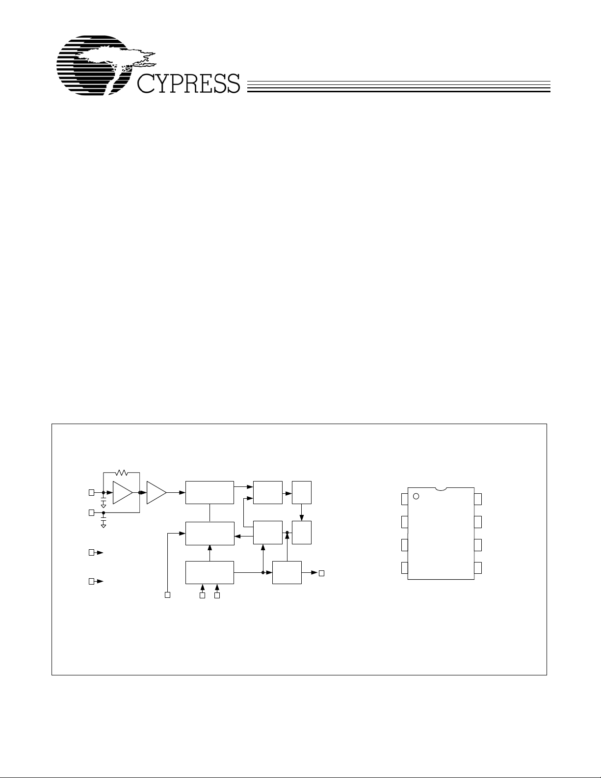
Block Diagram
300K
1
XIN
8pF
8
XOUT
8pF
7
VDD
VSS
2
FRSEL
REFERENCE
DIVIDER
MODULATION
CONTROL
INPUT
DECODER
LOGIC
3 46
S0
S1
PD and
CP
VCO
COUNTE
R
COUNTER
and
MUX
LF
VCO
5
SSCLK
Pin Configuration
XIN/CLKIN
1
2
VSS
3
S1
4
S0
8-pin SOIC/TSSOP
CY25811
CY25812
CY25814
8
XOUT
7
VDD
6
FRSEL
5
SSCLK
Cypress Semiconductor Corporation • 3901 North First Street • San Jose, CA 95134 • 408-943-2600
Document #: 38-07112 Rev. *E Revised June 03, 2004
CY25811/12/14
Pin Definitions
Pin No. Name Type Description
1Xin/CLK Crystal, ceramic resonator or clock input pin.
2VSS Power supply ground.
3S1 Digital Spread% control pin. 3-Level input (H-M-L). Default = M.
4S0 Digital Spread% control pin. 3-Level input (H-M-L). Default = M.
5 SSCLK Spread Spectrum output clock.
6 FRSEL Input frequency range selection digital control input. 3-Level input (H-M-L). Default = M.
7VDD Positive power supply.
8XOUT Crystal or ceramic resonator output pin.
Functional Description
The CY25811/12/14 products are Spread Spectrum Clock
Generator (SSCG) ICs used for the purpose of reducing
electromagnetic interference (EMI) found in today’s
high-speed digital electronic systems.
The devices use a Cypress proprietary phase-locked loop
(PLL) and Spread Spectrum Clock (SSC) technology to
synthesize and modulate the frequency of the input clock. By
frequency modulating the clock, the measured EMI at the
fundamental and harmonic frequencies is greatly reduced.
This reduction in radiated energy can significantly reduce the
cost of complying with regulatory agency requirements and
improve time to market without degrading system performance.
The input frequency range is 4 to 32 MHz and accepts clock,
crystal and ceramic resonator inputs. The output clock can be
selected to produce 1x, 2x, or 4x multiplication of the input
frequency with Spread Spectrum Frequency Modulation.
The use of 2x or 4x frequency multiplication eliminates the
need for higher order crystals and enables the user to
generate up to 128-MHz Spread Spectrum Clock (SSC) by
using only first order crystals. This will reduce the cost while
improving the system clock accuracy, performance and
complexity.
Center Spread or Down Spread frequency modulation can be
selected by the user based on four discrete values of
Table 2. Spread% Selection
XIN
(MHz) FRSEL
4-5 0 ±1.4 ± 1.2 ± 0.6 ± 0.5 –3.0 –2.2 –1.9 –0.7 0
5-6 0 ±1.3 ± 1.1 ± 0.5 ± 0.4 –2.7 –1.9 –1.7 –0.6 0
6-7 0 ±1.2 ± 0.9 ± 0.5 ± 0.4 –2.5 –1.8 –1.5 –0.6 0
7-8 0 ±1.1 ± 0.9 ± 0.4 ± 0.3 –2.3 –1.7 –1.4 –0.5 0
8-10 1 ±1.4 ±1.2 ± 0.6 ± 0.5 –3.0 –2.2 –1.9 –0.7 0
10-12 1 ±1.3 ±1.1 ± 0.5 ± 0.4 –2.7 –1.9 –1.7 –0.6 0
12-14 1 ±1.2 ± 0.9 ± 0.5 ± 0.4 –2.5 –1.8 –1.5 –0.6 0
14-16 1 ±1.1 ± 0.9 ± 0.4 ± 0.3 –2.3 –1.7 –1.4 –0.5 0
16-20 M ±1.4 ±1.2 ± 0.6 ± 0.5 –3.0 –2.2 –1.9 –0.7 0
S1 = 0
S0 = 0
Center
(%)
S1 = 0
S0 = M
Center
(%)
S1 = 0
S0 = 1
Center
(%)
Spread % for each Spread Mode with the option of a
Non-Spread mode for system test and verification purposes.
The CY25811/12/14 products are available in an 8-pin SOIC
(150-mil.) package with a Commercial operating temperature
range of 0 to 70°C and Industrial Temperature range of –40 to
85°C. Refer to CY25568 for multiple clock output options such
as modulated and unmodulated clock outputs or Power-down
function. For Automotive applications, refer to
CY25811/12/14SE data sheet.
Input Frequency Range and Selection
The CY25811/12/14 input frequency range is 4 to 32 MHz.
This range is divided into three segments and controlled by
3-Level FRSEL pin as given in Table 1.
Table 1. Input Frequency Selection
FRSEL Input Frequency Range
0 4.0 to 8.0 MHz
1 8.0 to 16.0 MHz
M 16.0 to 32.0 MHz
Spread% Selection
The CY25811/12/14 SSCG products provide Center-Spread,
Down-Spread and No-Spread functions. The amount of
Spread% is selected by using 3-Level S0 and S1 digital inputs
and Spread% values are given in Table 2.
S1 = M
S0 = 0
Center
(%)
S1 = 1
S0 = 1
Down
(%)
S1 = 1
S0 = 0
Down
(%)
S1 = M
S0 = 1
Down
(%)
S1 = 1
S0 = M
Down
(%) No Spread
S1 = M
S0 = M
Document #: 38-07112 Rev. *E Page 2 of 11
CY25811/12/14
Table 2. Spread% Selection (continued)
XIN
(MHz) FRSEL
20-24 M ±1.3 ±1.1 ± 0.5 ± 0.4 –2.7 –1.9 –1.7 –0.6 0
24-28 M ±1.2 ± 0.9 ± 0.5 ± 0.4 –2.5 –1.8 –1.5 –0.6 0
28-32 M ±1.1 ± 0.9 ± 0.4 ± 0.3 –2.3 –1.7 –1.4 –0.5 0
3-Level Digital Inputs
S0, S1, and FRSEL digital inputs are designed to sense 3
different logic levels designated as High “1”, Low “0” and
Middle “M”. With this 3-Level digital input logic, the 3-Level
Logic is able to detect 9 different logic states.
S0, S1 and FRSEL pins include an on chip 20K (10K/10K)
resistor divider. No external application resistors are needed
to implement the 3-Level logic levels as shown below:
Logic Level “0”: 3–Level logic pin connected to GND.
Logic Level “M”: 3–Level logic pin left floating (no connection).
Logic Level “1”: 3–Level logic pin connected to V
Figure 1 illustrates how to implement 3–Level Logic.
S1 = 0
S0 = 0
S1 = 0
S0 = M
S1 = 0
S0 = 1
.
DD
S1 = M
S0 = 0
S1 = 1
S0 = 1
S1 = 1
S0 = 0
S1 = M
S0 = 1
S1 = 1
S0 = M
S1 = M
S0 = M
LOGIC
LOW (0)
S0, S1
and
FRSEL
to VSS
VSS
LOGIC
MIDDLE (M)
S0, S1
and
FRSEL
UNCONNECTED
Figure 1. 3–Level Logic
Modulation Rate
Spread Spectrum Clock Generators utilize frequency
modulation (FM) to distribute energy over a specific band of
frequencies. The maximum frequency of the clock (fmax) and
minimum frequency of the clock (fmin) determine this band of
frequencies. The time required to transition from fmin to fmax
and back to fmin is the period of the Modulation Rate. The
Modulation Rate of SSCG clocks are generally referred to in
terms of frequency, or
fmod = 1/Tmod.
The input clock frequency, fin, and the internal divider
determine the Modulation Rate.
In the case of CY25811/2/4 devices, the (Spread Spectrum)
modulation Rate, fmod, is given by the following formula:
fmod = fin/DR
where; fmod is the Modulation Rate, fin is the Input Frequency
and DR is the Divider Ratio as given in Ta b l e 3. Notice that
Input Frequency Range is set by FRSEL.
LOGIC
HIGH (H)
S0, S1
and
FRSEL
to VDD
Table 3. Modulation Rate Divider Ratios
FRSEL
Input Frequency Range
(MHz)
Divider Ratio
(DR)
0 4 to 8 128
1 8 to 16 256
M 16 to 32 512
Input and Output Frequency Selection
The relationship between input frequency versus output
frequency in terms of device selection and FRSEL setting is
given in Table 4 . As shown, the input frequency range is
selected by FRSEL and is the same for CY25811, CY25812,
and CY25814. The selection of CY25811 (1x), CY25812 (2x)
or CY25814 (4x) determines the frequency multiplication at
the output (SSCLK, Pin 5) with respect to input frequency
(XIN, Pin-1).
Document #: 38-07112 Rev. *E Page 3 of 11
CY25811/12/14
Table 4. Input and Output Frequency Selection
Input Frequency Range
(MHz) FRSEL Product Multiplication
4 to 8 0 CY25811 1x 4 to 8
8 to 16 1 CY25811 1x 8 to 16
16 to 32 M CY25811 1x 16 to 32
4 to 8 0 CY25812 2x 8 to 16
8 to 16 1 CY25812 2x 16 to 32
16 to 32 M CY25812 2x 32 to 64
4 to 8 0 CY25814 4x 16 to 32
8 to 16 1 CY25814 4x 32 to 64
16 to 32 M CY25814 4x 64 to 128
Absolute Maximum Conditions (both Commercial and Industrial Grades)
[1,2]
Parameter Description Condition Min. Max. Unit
V
DD
V
IN
T
S
T
A1
T
A2
T
J
ESD
HBM
Supply Voltage –0.5 4.6 V
Input Voltage Relative to V
SS
Temperature, Storage Non Functional –65 150 °C
Temperature, Operating Ambient Functional, C-Grade 0 70 °C
Temperature, Operating Ambient Functional, I-Grade –40 85 °C
Temperature, Junction Functional – 150 °C
ESD Protection (Human Body Model) MIL-STD-883, Method 3015 2000 – V
UL-94 Flammability Rating @1/8 in. V–0
MSL Moisture Sensitivity Level 1
Output Frequency Range
(MHz)
–0.5 VDD + 0.5 VDC
DC Electrical Specifications (Commercial Grade)
Parameter Description Condition Min. Max. Unit
3.3 Operating Voltage 3.3 ± 5% 3.135 3.465 V
V
DD
V
IL
V
IM
V
IH
V
OL1
V
OL2
V
OH1
V
OH2
C
IN1
C
IN2
C
L
I
DD1
I
DD2
I
DD3
Notes:
1. Operation at any Absolute Maximum Rating is not implied.
2. Single Power Supply: The voltage on any input or I/O pin cannot exceed the power pin during power up.
Input Low Voltage S0, S1 and FRSEL Inputs 0 0.15V
Input Middle Voltage S0, S1 and FRSEL Inputs 0.40VDD0.60V
Input High Voltage S0, S1 and FRSEL Inputs 0.85V
DD
DD
DD
V
DD
Output Low Voltage IOL = 4 ma, SSCLK Output – 0.4 V
Output Low Voltage IOL = 10 ma, SSCLK Output – 1.2 V
Output High Voltage IOH = 4 ma, SSCLK Output 2.4 – V
Output High Voltage IOH = 6 ma, SSCLK Output 2.0 – V
Input Pin Capacitance XIN (Pin 1) and XOUT (Pin 8) 6.0 9.0 pF
Input Pin Capacitance All Digital Inputs 3.5 6.0 pF
Output Load Capacitor SSCLK Output – 15 pF
Dynamic Supply Current Fin = 12 MHz, no load – 25 mA
Dynamic Supply Current Fin = 24 MHz, no load – 30 mA
Dynamic Supply Current Fin = 32 MHz, no load – 35 mA
V
V
V
Document #: 38-07112 Rev. *E Page 4 of 11
CY25811/12/14
AC Electrical Specifications (Commercial Grade)
Parameter Description Condition Min. Max. Unit
F
IN
T
R1
T
F1
T
R2
T
F2
T
DCIN
T
DCOUT
T
CCJ1
T
CCJ2
T
CCJ3
T
CCJ4
T
CCJ5
T
CCJ6
T
SU
DC Electrical Specifications (Industrial Grade)
Parameter Description Condition Min. Max. Unit
3.3 Operating Voltage 3.3 ± 5% 3.135 3.465 V
V
DD
V
IL
V
IM
V
IH
V
OL1
V
OL2
V
OH1
V
OH2
C
IN1
C
IN2
C
L
I
DD1
I
DD2
I
DD3
Input Frequency Range Clock, Crystal or Ceramic Resonator Input 4 32 MHz
Clock Rise Time SSCLK, CY25811 and CY25812 2.0 5.0 ns
Clock Fall Time SSCLK, CY25811 and CY25812 2.0 4.4 ns
Clock Rise Time SSCLK, only CY25814 when FRSEL = M 1.0 2.2 ns
Clock Fall Time SSCLK, only CY25814 when FRSEL = M 1.0 2.2 ns
Input Clock Duty Cycle XIN 40 60 %
Output Clock Duty Cycle SSCLK 40 60 %
Cycle-to-Cycle Jitter, Spread on Fin = 4 MHz, Fout = 4 MHz, CY25811 – 800 ps
Cycle-to-Cycle Jitter, Spread on Fin = 8 MHZ, Fout = 8 MHz, CY25811 – 450 ps
Cycle-to-Cycle Jitter, Spread on Fin = 8 MHz, Fout = 16 MHz, CY25812 – 400 ps
Cycle-to-Cycle Jitter, Spread on Fin = 16 MHz, Fout = 32 MHz, CY25812 – 380 ps
Cycle-to-Cycle Jitter, Spread on Fin = 16 MHz, Fout = 64 MHz, CY25814 – 380 ps
Cycle-to-Cycle Jitter, Spread on Fin = 32 MHz, Fout = 128 MHz, CY25814 – 380 ps
PLL Lock Time Fom V
Input Low Voltage S0, S1 and FRSEL Inputs 0 0.13V
Input Middle Voltage S0, S1 and FRSEL Inputs 0.40VDD0.60V
Input High Voltage S0, S1 and FRSEL Inputs 0.85V
3.0V to valid SSCLK – 3 ms
DD
DD
DD
V
DD
DD
Output Low Voltage IOL = 4 ma, SSCLK Output – 0.4 V
Output Low Voltage IOL = 10 ma, SSCLK Output – 1.2 V
Output High Voltage IOH = 4 ma, SSCLK Output 2.4 – V
Output High Voltage IOH = 6 ma, SSCLK Output 2.0 – V
Input Pin Capacitance XIN (Pin 1) and XOUT (Pin 8) 6.0 9.0 pF
Input Pin Capacitance All Digital Inputs 3.5 6.0 pF
Output Load Capacitor SSCLK Output – 15 pF
Dynamic Supply Current Fin = 12 MHz, no load – 26 mA
Dynamic Supply Current Fin = 24 MHz, no load – 32 mA
Dynamic Supply Current Fin = 32 MHz, no load – 37 mA
V
V
V
AC Electrical Specifications (Industrial Grade)
Parameter Description Condition Min. Max. Unit
F
IN
T
R1
T
F1
T
R2
T
F2
T
DCIN
T
DCOUT
T
CCJ1
T
CCJ2
T
CCJ3
T
SU
Document #: 38-07112 Rev. *E Page 5 of 11
Input Frequency Range Clock, Crystal or Ceramic Resonator Input 4 32 MHz
Clock Rise Time SSCLK, CY25811 and CY25812 2.0 5.0 ns
Clock Fall Time SSCLK, CY25811 and CY25812 2.0 4.4 ns
Clock Rise Time SSCLK, only CY25814 when FRSEL = M 1.0 2.2 ns
Clock Fall Time SSCLK, only CY25814 when FRSEL = M 1.0 2.2 ns
Input Clock Duty Cycle XIN 40 60 %
Output Clock Duty Cycle SSCLK 40 60 %
Cycle-to-Cycle Jitter, Spread on Fin = 6MHz, CY25811/12/14 – 650 ps
Cycle-to-Cycle Jitter, Spread on Fin = 12MHZ, CY25811/12/14 – 400 ps
Cycle-to-Cycle Jitter, Spread on Fin = 24MHz, CY25811/12/14 – 400 ps
PLL Lock Time From V
3.0V to valid SSCLK – 4 ms
DD
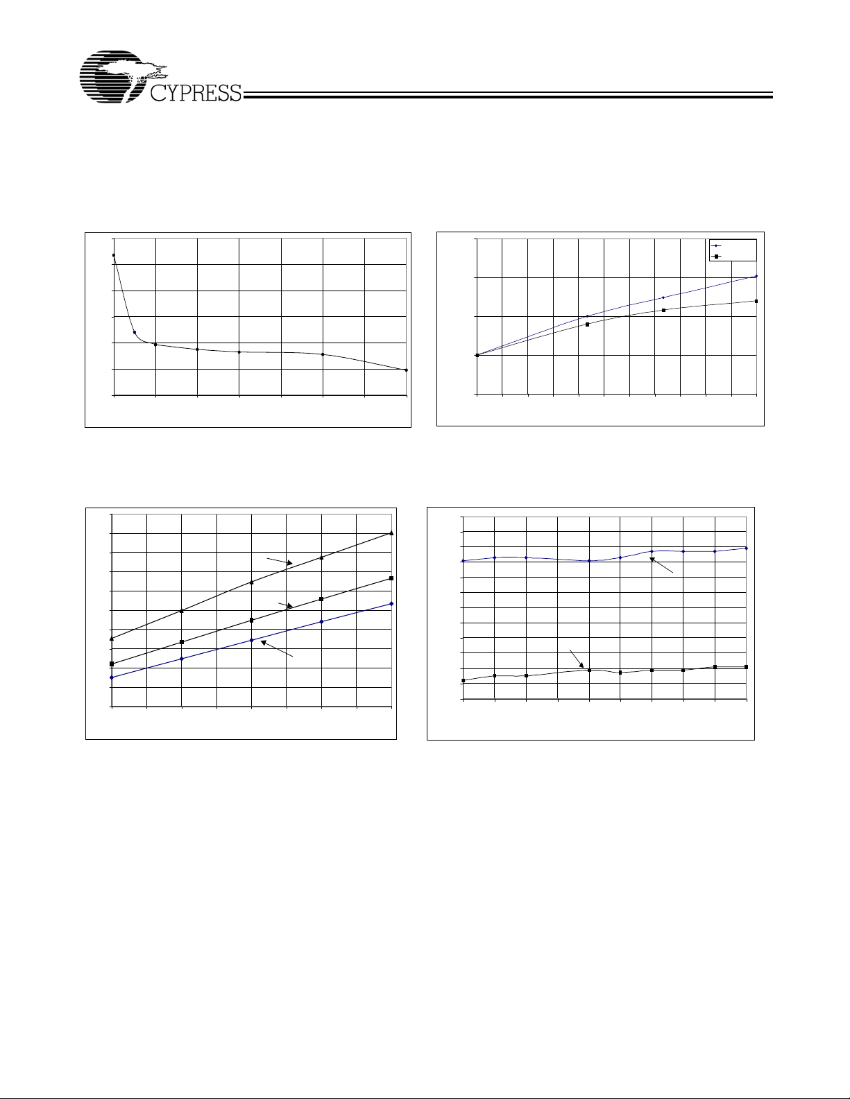
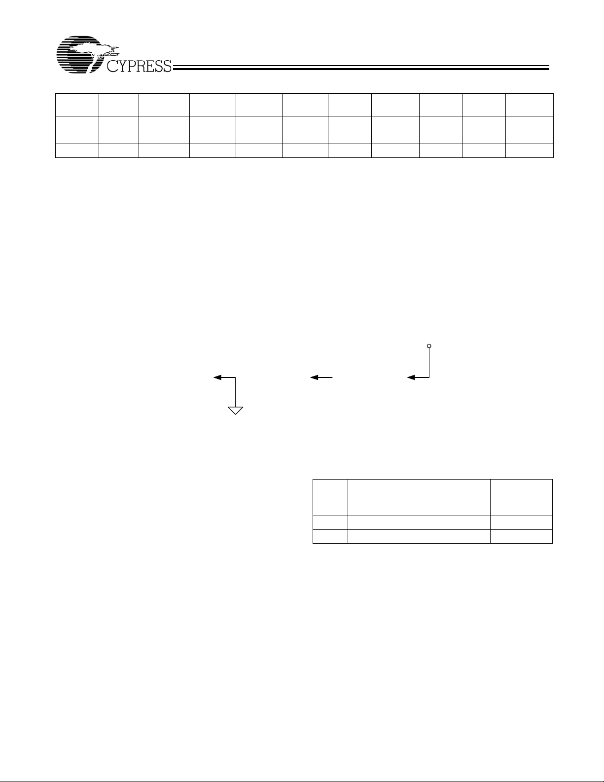
Characteristic Curves
The following curves demonstrate the characteristic behavior
of the CY25811/12/14 when tested over a number of environmental and application-specific parameters. These are typical
performance curves and are not meant to replace any
parameter specified in DC and AC Specification tables.
CY25811/12/14
600
500
400
300
CCJ (ps)
200
100
0
4 8 12 16 20 24 28 32
Input Frequency ( MHz)
Jitter vs. Input Frequency (No Load)
30
28
26
24
22
20
IDD (mA)
18
16
14
12
10
4 4.5 5 5.5 6 6.5 7 7.5 8
Frequency (MHz), no load, normali zed to FRSEL = 0, (4 - 8 MHz).
FRSEL = M
16 - 32 MHz
FRSEL = 1
8 - 16 MHz
FRSEL = 0
4 - 8 MHz
2.75
2.5
2.25
BW %
2
1.75
-40 -25 -10 5 20 35 50 65 80 95 110 125
Bandwidth % vs. Temperature
Temp (C)
6.0 MHz
32.0 M Hz
3
2.9
2.8
2.7
2.6
4.0 MHz
2.5
2.4
BW (%)
2.3
2.2
8.0 MHz
2.1
2
1.9
1.8
2.8 2.9 3 3.1 3.2 3.3 3.4 3.5 3.6 3.7
VDD (volts)
IDD vs. Frequency (FRSEL = 0, 1, M)
Bandwidth % vs. VDD
Figure 2. Characteristic Curves
Document #: 38-07112 Rev. *E Page 6 of 11
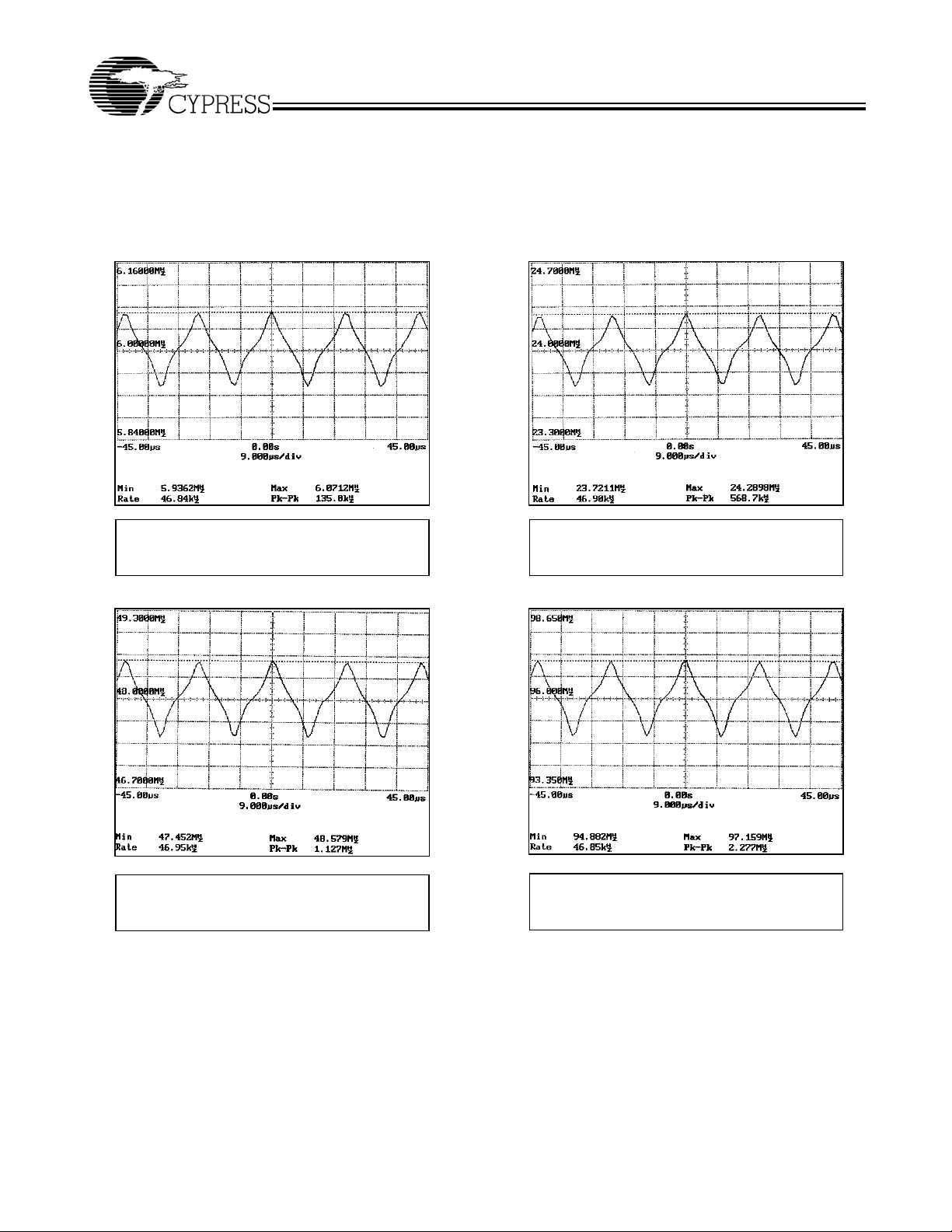
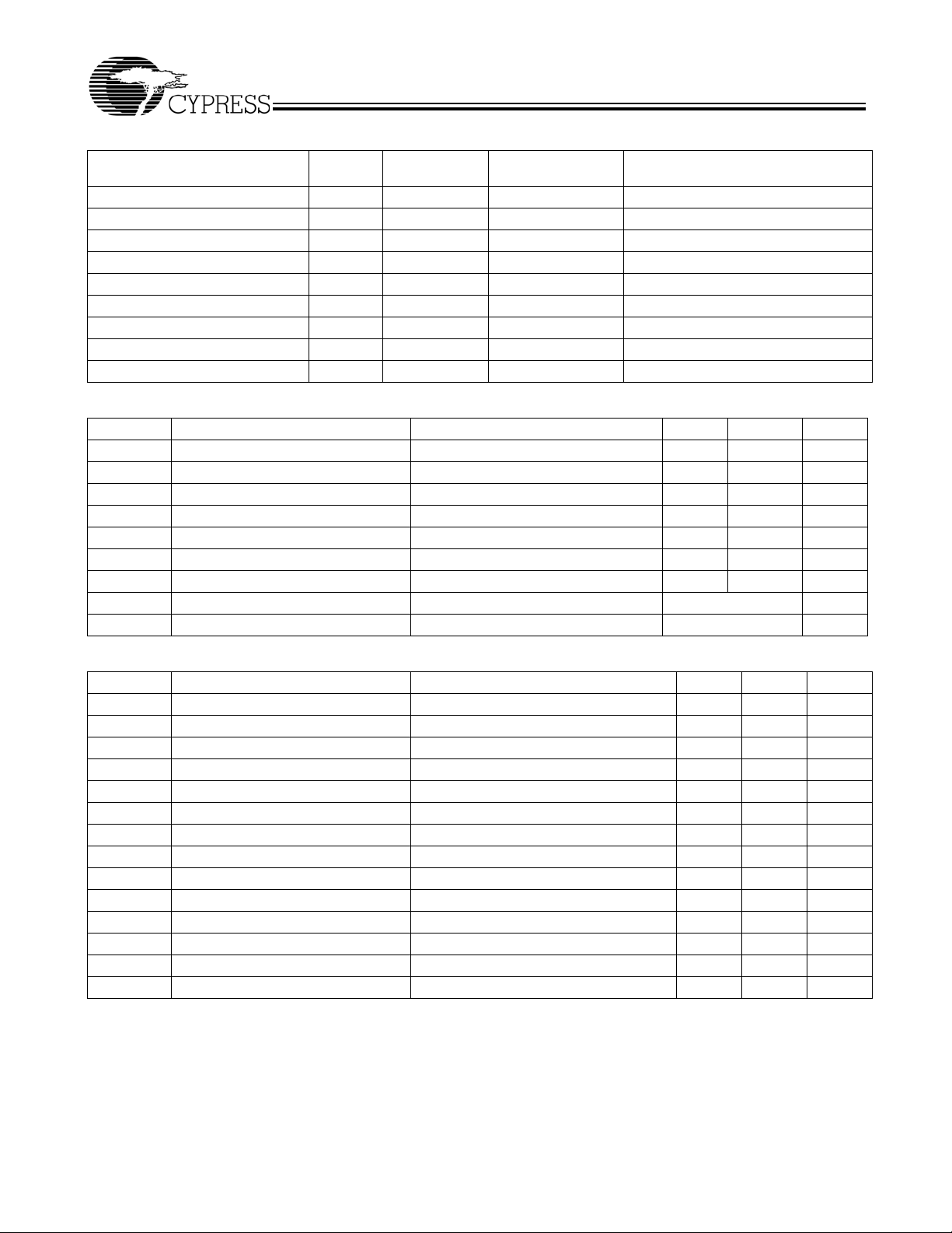
SSCG Profiles
CY25811/12/14 SSCG products use a non-linear “optimized”
frequency profile as shown In Figure 3. The use of Cypress
proprietary “optimized” frequency profile maintains flat energy
distribution over the fundamental and higher order harmonics.
This results in additional EMI reduction in electronic systems.
CY25811/12/14
Xin = 6.0 MHz SSCLK1 = 6.0 MHz
S1, S0 = 0
FRSEL = 0 P/N = CY25811
Xin = 12.0 MHz SSCLK1 = 48.0 MHz
S1, S0 = 0
FRSEL = 1 P/N = CY25814
Figure 3. Spread Spectrum Profiles (Frequency vs. Time)
Xin = 24.0 MHz SSCLK1 = 24.0 MHz
S1, S0 = 0
FRSEL = M P/N = CY25811
Xin = 24.0 MHz SSCLK1 = 96.0 MHz
S1, S0 = 0
FRSEL = M P/N = CY25814
Document #: 38-07112 Rev. *E Page 7 of 11

Application Schematic
C3
CY25811/12/14
VDD
0.1 uF
C2
27 pF
C3
27 pF
1
Y1
25 MHz
8
XIN
XOUT
7
VDD
CY25811
SSCLK
25 MHz (CY25811)
5
50 MHz (CY25812)
100 MHz (CY25814)
CY25812
CY25814
3
S1
S0
4
N/C
6
FRSEL
VSS
2
Ordering Information
Part Number Package Type Product Flow
CY25811SC 8-pin SOIC Commercial, 0
CY25811SCT 8-pin SOIC – Tape and Reel Commercial, 0
CY25811SI 8-pin SOIC Industrial, –40° to 85°C
CY25811SIT 8-pin SOIC – Tape and Reel Industrial, –40° to 85°C
CY25811ZC 8-pin TSSOP Commercial, 0
CY25811ZCT 8-pin TSSOP – Tape and Reel Commercial, 0
CY25812SC 8-pin SOIC Commercial, 0
CY25812SCT 8-pin SOIC – Tape and Reel Commercial, 0
CY25812SI 8-pin SOIC Industrial, –40° to 85°C
CY25812SIT 8-pin SOIC – Tape and Reel Industrial, –40° to 85°C
CY25812ZC 8-pin TSSOP Commercial, 0
CY25812ZCT 8-pin TSSOP – Tape and Reel Commercial, 0
CY25814SC 8-pin SOIC Commercial, 0
CY25814SCT 8-pin SOIC – Tape and Reel Commercial, 0
CY25814SI 8-pin SOIC Industrial, –40° to 85°C
CY25814SIT 8-pin SOIC – Tape and Reel Industrial, –40° to 85°C
CY25814ZC 8-pin TSSOP Commercial, 0
CY25814ZCT 8-pin TSSOP – Tape and Reel Commercial, 0
Lead Free Devices
CY25811SXC 8-pin SOIC Commercial, 0
CY25811SXCT 8-pin SOIC – Tape and Reel Commercial, 0
CY25811SXI 8-pin SOIC Industrial, –40° to 85°C
CY25811SXIT 8-pin SOIC – Tape and Reel Industrial, –40° to 85°C
° to 70°C
° to 70°C
° to 70°C
° to 70°C
° to 70°C
° to 70°C
° to 70°C
° to 70°C
° to 70°C
° to 70°C
° to 70°C
° to 70°C
° to 70°C
° to 70°C
Document #: 38-07112 Rev. *E Page 8 of 11
Ordering Information (continued)
CY25811ZXC 8-pin TSSOP Commercial, 0° to 70°C
CY25811ZXCT 8-pin TSSOP – Tape and Reel Commercial, 0
CY25812SXC 8-pin SOIC Commercial, 0
CY25812SXCT 8-pin SOIC – Tape and Reel Commercial, 0
° to 70°C
° to 70°C
° to 70°C
CY25812SXI 8-pin SOIC Industrial, –40° to 85°C
CY25812SXIT 8-pin SOIC – Tape and Reel Industrial, –40° to 85°C
CY25812ZXC 8-pin TSSOP Commercial, 0
CY25812ZXCT 8-pin TSSOP – Tape and Reel Commercial, 0
CY25814SXC 8-pin SOIC Commercial, 0
CY25814SXCT 8-pin SOIC – Tape and Reel Commercial, 0
° to 70°C
° to 70°C
° to 70°C
° to 70°C
CY25814SXI 8-pin SOIC Industrial, –40° to 85°C
CY25814SXIT 8-pin SOIC – Tape and Reel Industrial, –40° to 85°C
CY25814ZXC 8-pin TSSOP Commercial, 0
CY25814ZXCT 8-pin TSSOP – Tape and Reel Commercial, 0
° to 70°C
° to 70°C
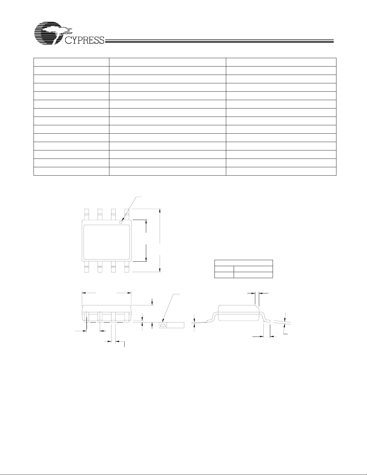
Package Drawing and Dimensions
8-lead (150-Mil) SOIC S8
PIN1ID
14
CY25811/12/14
0.050[1.270]
BSC
0.150[3.810]
0.157[3.987]
0.230[5.842]
0.244[6.197]
58
0.189[4.800]
0.196[4.978]
0.061[1.549]
0.068[1.727]
0.004[0.102]
0.0098[0.249]
0.0138[0.350]
0.0192[0.487]
0.004[0.102]
SEATING PLANE
0°~8°
1. DIMENSIONS IN INCHES[MM] MIN.
2. PIN1IDISOPTIONAL,
ROUND ON SINGLE LEADFRAME
RECTANGULAR ON MATRIX LEADFRAME
3. REFERENCE JEDEC MS-012
4. PACKAGE WEIGHT 0.07gms
S08.15 STANDARD PKG.
SZ08.15 LEAD FREE PKG.
PART #
0.016[0.406]
0.035[0.889]
MAX.
0.010[0.254]
0.016[0.406]
X 45°
0.0075[0.190]
0.0098[0.249]
51-85066-*C
Document #: 38-07112 Rev. *E Page 9 of 11

CY25811/12/14
8-Lead Thin Shrunk Small Outline Package (4.40 MM Body) Z8
1
PIN1ID
DIMENSIONS IN MM[INCHES] MIN.
MAX.
6.25[0.246]
6.50[0.256]
4.30[0.169]
4.50[0.177]
8
0.65[0.025]
0.19[0.007]
0.30[0.012]
0.85[0.033]
0.95[0.037]
2.90[0.114]
3.10[0.122]
BSC.
0.05[0.002]
0.15[0.006]
1.10[0.043] MAX.
0.076[0.003]
SEATING
PLANE
Intel and Pentium are registered trademarks of Intel Corporation. All product and company names mentioned in this document
are the trademarks of their respective holders.
GAUGE
PLANE
0.25[0.010]
BSC
0°-8°
0.50[0.020]
0.70[0.027]
0.09[[0.003]
0.20[0.008]
51-85093-*A
Document #: 38-07112 Rev. *E Page 10 of 11
© Cypress Semiconductor Corporation, 2004. The information contained herein is subject to change without notice. Cypress Semiconductor Corporation assumes no responsibility for the use
of any circuitry other than circuitry embodied in a Cypress product. Nor does it convey or imply any license under patent or other rights. Cypress products are not warranted nor intended to be
used for medical, life support, life saving, critical control or safety applications, unless pursuant to an express written agreement with Cypress. Furthermore, Cypress does not authorize its
products for use as critical components in life-support systems where a malfunction or failure may reasonably be expected to result in significant injury to the user. The inclusion of Cypress
products in life-support systems application implies that the manufacturer assumes all risk of such use and in doing so indemnifies Cypress against all charges.
CY25811/12/14
Document History Page
Document Title: CY25811/12/14 Spread Spectrum Clock Generator
Document Number: 38-07112
REV. ECN NO.
Date
** 107516 06/14/02 NDP Converted from IMI to Cypress
*A 108002 06/29/02 NDP Deleted Junction Temp. in Absolute Maximum Ratings
*B 121578 01/29/03 RGL Converted from Word to FrameMaker
*C 125550 05/14/03 RGL Changed IDD values from 19.6/22/27.2 to 25/30/35 in Commercial Grade DC Specs
*D 131941 12/24/03 RGL Removed automotive in the Applications section
*E 231057 See ECN RGL Added Lead Free Devices
Issue
Orig. of
Change Description of Change
Added 8-pin TSSOP package in Commercial Temp. only
Added an Industrial Temperature Range to all existing 8-pin SOIC packages
table
Changed IDD values from 24/26.5/33 to 26/32/37 in Industrial grade DC Specs table
Changed T
Changed T
Changed the Output Clock Duty Cycle (T
60% respectively for both industrial and commercial grade
Changed the min. Input Low Voltage (V
Removed preliminary from the industrial AC/DC Electrical Specifications table
values from 675/260 to 800/450 in Commercial grade AC Specs table
CCJ1/2
value from 350 to 650 in Industrial grade AC Specs table
CCJ1
) from min. 45 and max. 55 to 40 and
DCOUT
) from 0.15VDD to 0.13V
IL
DD
Document #: 38-07112 Rev. *E Page 11 of 11
 Loading...