

CY25701JXC/FJXC
Programmable High-Frequency Crystal Oscillator with Spread
Spectrum (SSXO) and No-Spread Spectrum (XO) Option
Features
• Crystal Oscillator with Spread Sp ectrum Clock (SSXO)
• No-Spread Spectrum (XO) Option
• Wide operating output clock frequency range of
10–166 MHz
• Programmable spread spectrum with nominal 31.5-kHz
modulation frequency
• Center spread: ±0.25% to ±2.0%
• Down spread: –0.5% to –4.0%
• No spread: ± 0.0%
• Integrated phase-locked loop (PLL)
• 85 ps typical cycle-to-cycle Jitter with SSCLK = 133MHz
• 3.3V operation
• Output Enable function
• Package available in 4-pin Plastic JE
• Pb-free package
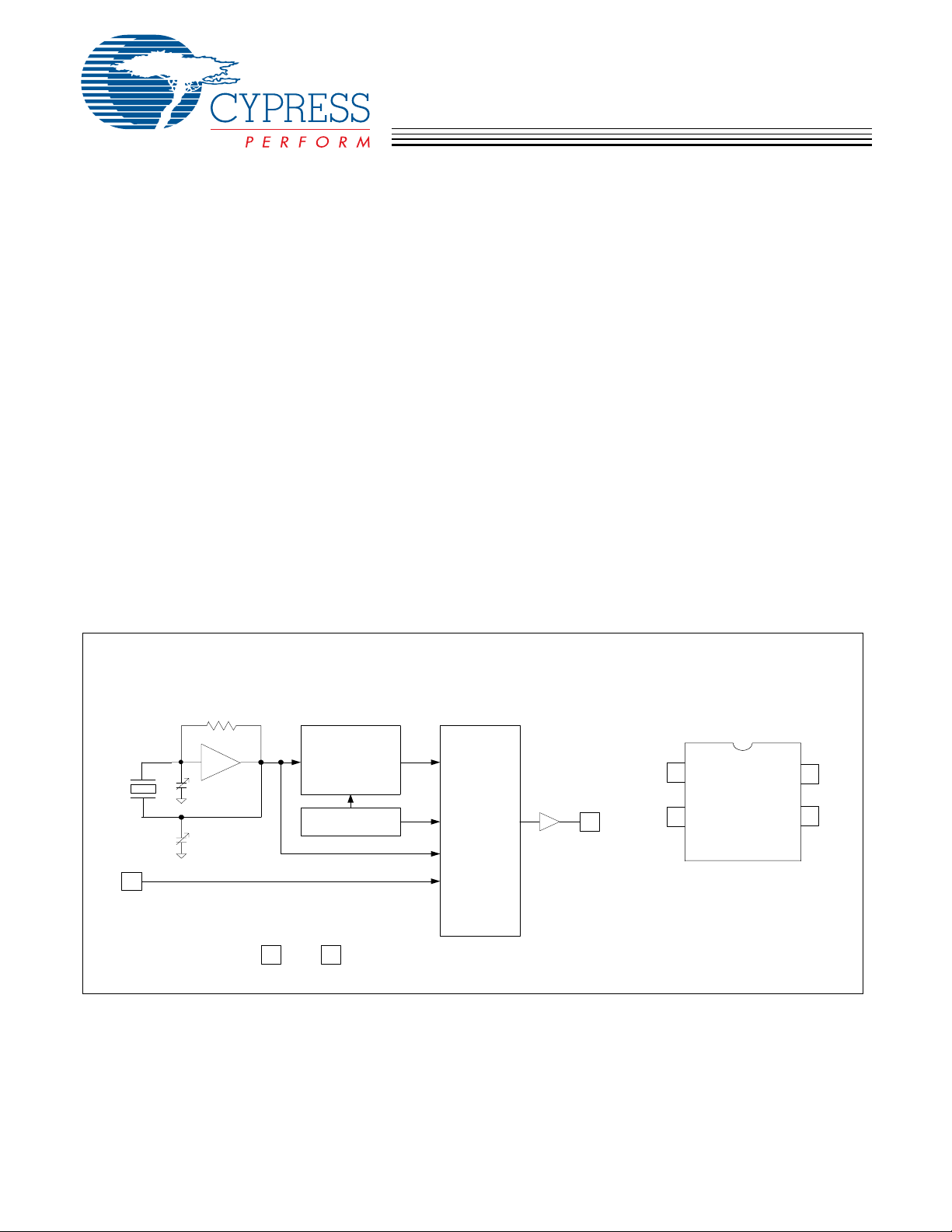
Logic Block Diagram
RFB
Benefits
• Provides wide range of spread percentages for
maximum electromagnetic interference (EMI)
reduction, to meet regulatory agency electromagnetic
compliance (EMC) requirements. Reduces development and manufacturing costs and time-to-market.
• This versatile programming feature enables the users
to switch between SSXO (with Spread) and XO (without
Spread) functions with ease.
• Internal PLL to generate up to 166-MHz output.
• Suitable for most PC, consumer, and networking
applications
• Application compatibility in standard and low-power
systems
• In-house programming of samples and prototype
quantities is available using the CY3672 programming
kit and CY3613 (JEC package) socket adapters.
Production quantities are available through Cypress’
value-added distribution partners or by using
third-party programmers from BP Microsystems, HiLo
Systems, and others.
Pin Configuration
CY25701JXC/FJXC
4-pin Plastic JE
PLL
with
OE
MODULATION
CONTROL
CXIN
PROGRAMMABLE
CONFIGURATION
XOUT
C
1
4 2
VDD VSS
OUTPUT
DIVIDERS
and
MUX
3
SSCLK
1
OE
2
VSS
SSCLK
VDD
4
3
Cypress Semiconductor Corporation • 198 Champion Court • San Jose, CA 95134-1709 • 408-943-2600
Document #: 38-07684 Rev. *E Revised March 27, 2006
[+] Feedback [+] Feedback
CY25701JXC/FJXC
Pin Definition
Pin Name Description
1OE Output Enable pin: Active HIGH. If OE = 1, SSCLK is enabled.
2 VSS Power supply ground.
3 SSCLK Spread spectrum clock output (with or without spread).
4VDD3.3V power supply.
Functional Description
The CY25701JXC/FJXC is a Spread Spectrum Crystal Oscillator (SSXO) IC used for the purpose of reducing EMI found in
today’s high-speed digital electronic systems.
The device uses a Cypress proprietary PLL and Spread
Spectrum Clock (SSC) technology to synthesize and modulate
the frequency of the embedded input crystal. By frequency
modulating the clock, the measured EMI at the fundamental
and harmonic frequencies are greatly reduced. This reduction
in radiated energy can significantly reduce the cost of
complying with regulatory agency (EMC) requirements and
improve time-to-market without degrading system performance.
The CY25701JXC/FJXC uses a programmable configuration
memory array to synthesize output frequency and spread%.
The spread% is programmed to either center spread or down
spread with various spread percentages. The range for center
spread is from ±0.25% to ±2.00%. The range for down spread
is from –0.5% to –4.0%. Contact the factory for smaller or
larger spread% amounts if required. Refer to Table 2 for
spread selection and no-spread values.
The frequency modulated SSCLK output can be programmed
from 10–166 MHz.
The CY25701JXC/FJXC is available in a 4-pin plastic package
with operating temperature range of –20 to 70°C.
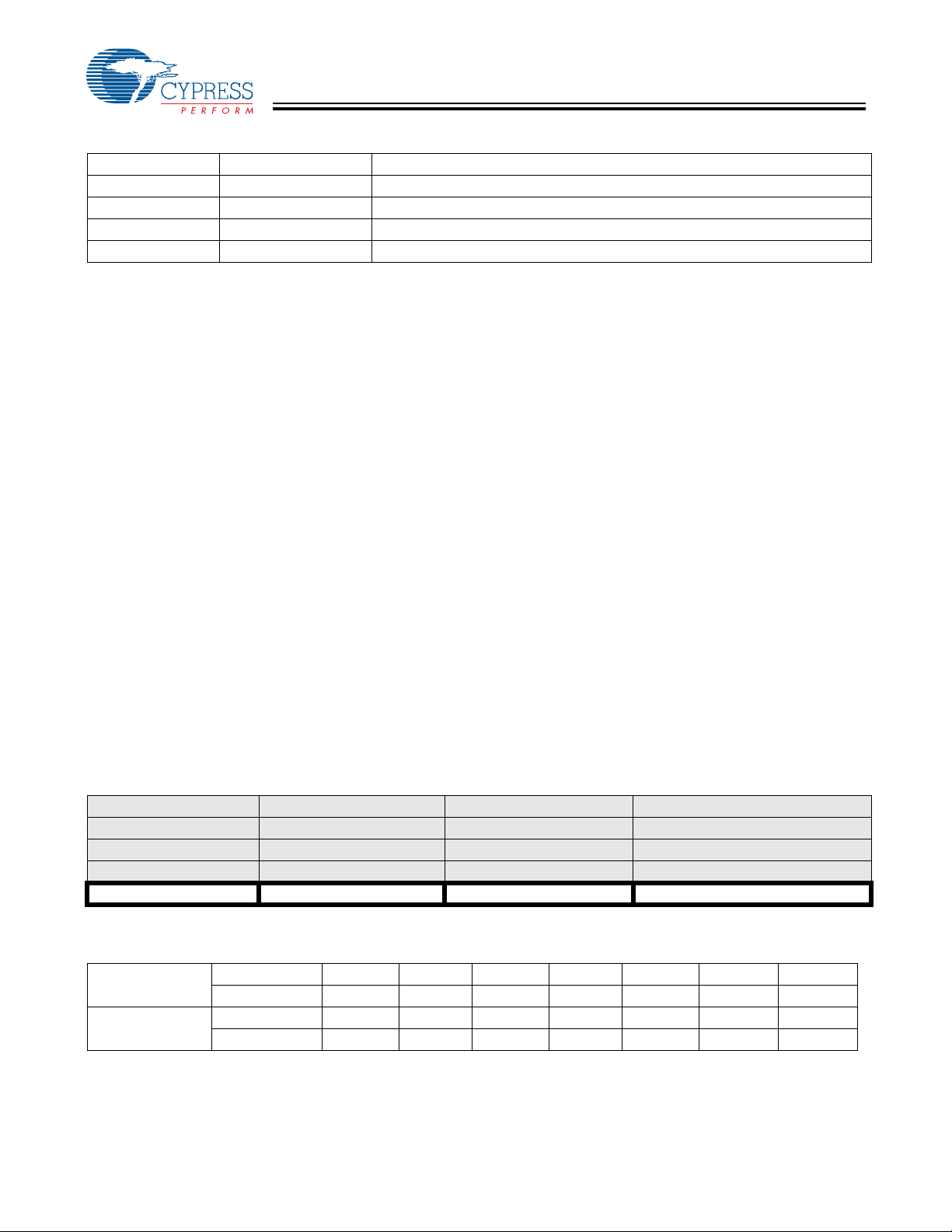
Table 1. Programming Data Requirement
Pin Function Output Frequency Spread Percent Code
Pin Name SSCLK SSCLK SSCLK
Pin# 3 3 3
Units MHz % kHz
Program Value ENTER DATA ENTER DATA 31.5
Programming Description
Field/Factory-Programmable CY25701JXC/FJXC
Field/Factory programming is available for samples and
manufacturing by Cypress and its distributors. All requests
must be submitted to the local Cypress Field Application
Engineer (FAE) or sales representative. Once the request has
been processed, you will receive a new part number, samples,
and data sheet with the programmed values. This part number
will be used for additional sample requests and production
orders.
Additional information on the CY25701JXC/FJXC can be
obtained from the Cypress web site at www.cypress.com.
Output Frequency, SSCLK Output (SSCLK, pin 3)
The modulated frequency at the SSCLK output is pr oduced by
synthesizing from the embedded crystal oscillator frequency
input. The range of synthesized clock is from 10–166 MHz.
Spread Percentage (SSCLK, pin 3)
The SSCLK spread can be programmed to various spread
percentage values from ±0.25% to ±2.0% for Center Spread
and from –0.5% to –4.0% for Down Spread. Refer to Table 2
for available spread options. Enter ±0.0% (No spread) for XO
(Crystal Oscillator) without spread option.
Frequency Modulation (SSCLK, pin 3)
The frequency modulation is programmed at 31.5 kHz for all
SSCLK frequencies from 10 to 166 MHz. Contact the factory
if a higher-modulation frequency is required.
[1]
Frequency Modulation
Table 2. Spread Percent Selection
Center Spread Code A B C D E F Z
Percentage ±0.25% ±0.5% ±0.75% ±1.0% ±1.5% ±2.0% ±0.0%
Down Spread Code G H J K L M Z
Percentage –0.5% –1.0% –1.5% –2.0% –3.0% –4.0% ±0.0%
Note:
1. ±0.0% or Code “Z” for XO (No-Spread) option.
Document #: 38-07684 Rev. *E Page 2 of 7
[+] Feedback [+] Feedback
CY25701JXC/FJXC
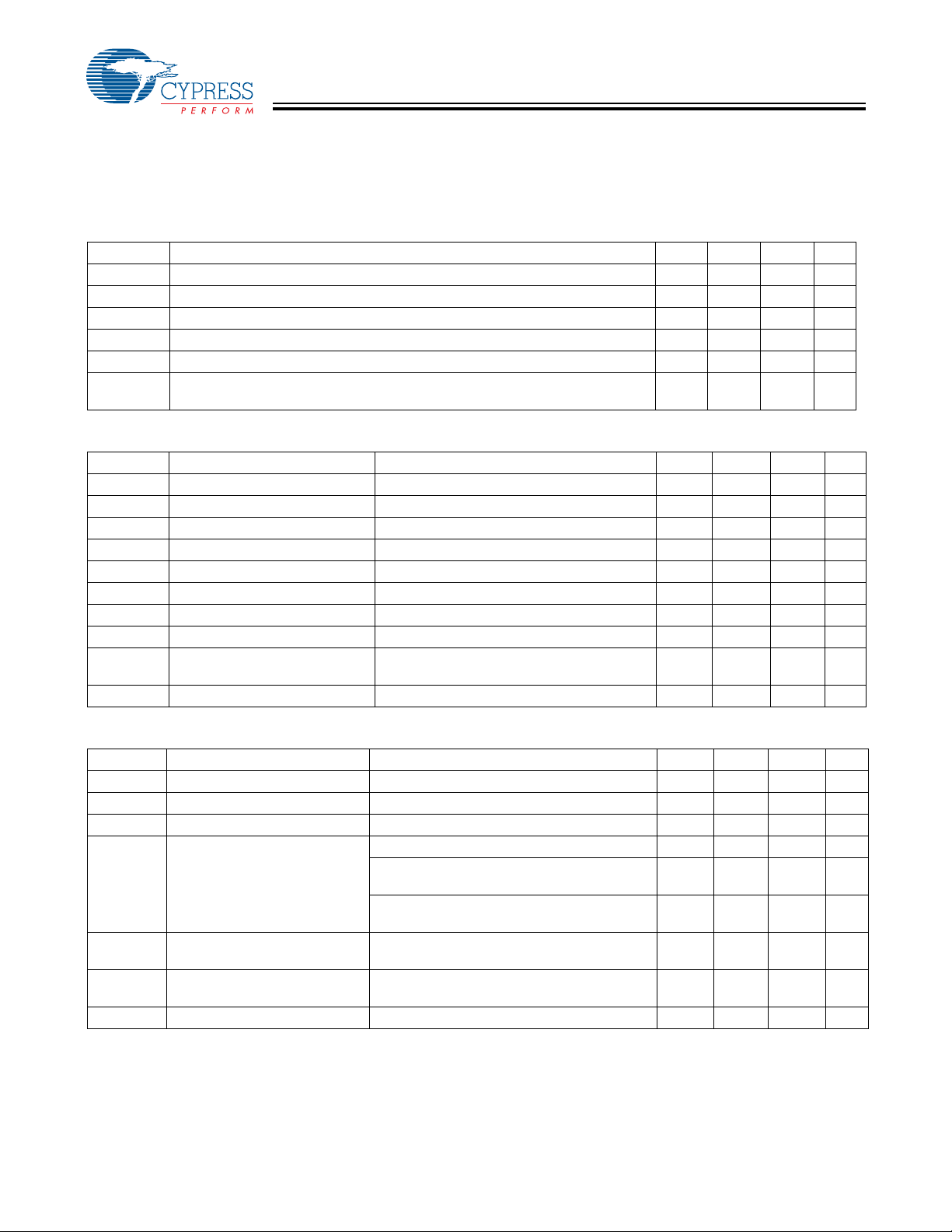
Absolute Maximum Rating
Supply Voltage (VDD)....................................–0.5V to +7.0V
DC Input Voltage....................................–0.5V to V
DD
+ 0.5V
Storage Temperature (Non-condensing) .... –55°C to +100°C
Junction Temperature................................ –40°C to +125°C
Data Retention @ Tj = 12 5°C................................> 10 years
Package Power Dissipation......................................350 mW
Operating Conditions
Parameter Description Min. Typ. Max. Unit
V
DD
T
A
C
LOAD
F
SSCLK
F
MOD
T
PU
Supply Voltage 3.00 3.30 3.60 V
Ambient Temperature –20 – 70 °C
Max. Load Capacitance @ pin 3 – – 15 pF
SSCLK output frequency, C
= 15 pF 10 – 166 MHz
LOAD
Spread Spectrum Modulation Frequency 30.0 31.5 33.0 kHz
Power-up time for VDD to reach minimum specified voltage (power ramp must
0.05 – 500 ms
be monotonic)
DC Electrical Characteristics
Parameter Description Condition Min. T yp. Max. Unit
I
OH
I
OL
V
IH
V
IL
I
IH
I
IL
I
OZ
[2]
C
IN
I
VDD
∆fAging T
Output High Current (pin 3) VOH = VDD – 0.5, V
= 3.3V (source) 10 12 – mA
DD
Output Low Current (pin 3) VOL = 0.5, VDD= 3.3V (sink) 10 12 – mA
Input High Voltage (pin 1) CMOS levels, 70% of V
Input Low Voltage (pin 1) CMOS levels, 30% of V
Input High Current (pin 1) V
Input Low Current (pin 1) V
= V
in
DD
= V
in
SS
DD
DD
0.7V
V
DD
SS
–VDDV
–0.3VDDV
––10µA
––10µA
Output Leakage Current (pin 3) Three-state output, OE = 0 –10 – 10 µA
Input Capacitance (pin 1) Pin 1, or OE – 5 7 pF
Supply Current V
= 3.3V , SSCLK = 10 to 166 MHz, C
DD
= 0, OE = V
= 25°C, First year –5 – 5 ppm
A
DD
LOAD
––50mA
AC Electrical Characteristics
[2]
Parameter Description Condition Min. Typ. Max. Unit
DC Output Duty Cycle SSCLK, Measured at V
t
R
t
F
T
CCJ1
Output Rise Time 20%–80% of V
Output Fall Time 20%–80% of V
[3]
Cycle-to-Cycle Jitter SSCLK
(Pin 3)
DD, CL
DD, CL
SSCLK ≥133 MHz, Measured at VDD/2 – 85 200 ps
25 MHz ≤ SSCLK <133 MHz, Measured at
V
/2
DD
SSCLK < 25 MHz, Measured at V
T
OE1
T
OE2
T
LOCK
Notes:
2. Guaranteed by characterization, not 100% tested.
3. Jitter is configuration dependent. Actual jitter is dependent on output frequencies, spread percent age, temperature , and output load. For more information, refer
to the application note, “Jitter in PLL Based Systems: Causes, Effect s, and Solutio ns” available at http: //www .cypress.com/ clock/appnotes.html, or contact your
local Cypress Field Application Engineer.
Output Disable Time (pin1 = OE) Time from falling edge on OE to stopped
outputs (Asynchronous)
Output Enable Time (pin1 = OE) Time from rising edge on OE to outputs at a
valid frequency (Asynchronous)
PLL Lock Time Time for SSCLK to reach valid frequency – – 10 ms
/2 45 50 55 %
DD
= 15 pF – – 2.7 ns
= 15 pF – – 2.7 ns
– 215 400 ps
/2 – – 1% of
DD
1/SSCK
– 150 350 ns
– 150 350 ns
s
Document #: 38-07684 Rev. *E Page 3 of 7
[+] Feedback [+] Feedback

Application Circuit
CY25701JXC/FJXC
4
VDD
0.1 µF
SSCLK
Power
CY25701
OE
1
VDD
Figure 1. Application Circuit Diagram
VSS
Switching Waveforms
Duty Cycle Timing (DC = t1A/t1B)
SSCLK
t
3
2
t
1B
1A
Figure 2. Duty Cycle Waveform
Output Rise/Fall Time
SSCLK
Tr
Output Rise time (Tr) = (0.6 x VDD)/SR1 (or SR3)
Output Fall time (Tf) = (0.6 x VDD)/SR2 (or SR4)
Refer to AC Electrical Characteristics table for SR (Slew Rate) values.
Figure 3. Output Rise/Fall Time Waveform
Output Enable/Disable Timing
V
OUTPUT
DD
ENABLE
0V
(Asynchronous
SSCLK
)
Figure 4. Output Enable/Disable Timing Waveforms
Tf
V
IL
High Impedance
T
OE1
V
DD
0V
V
IH
T
OE2
Document #: 38-07684 Rev. *E Page 4 of 7
[+] Feedback [+] Feedback

CY25701JXC/FJXC
4
Informational Graphs
172.5
171.5
170.5
Spread Spectrum Profile: Fnom=166MHz,
Fmod =30kHz , S p r e ad%= -4%
169.5
168.5
167.5
166.5
165.5
164.5
163.5
162.5
161.5
160.5
159.5
0 20 40 60 80 100 120 140 160 180 200
68.5
68
67.5
67
66.5
66
65.5
65
64.5
6
63.5
Spread Spectrum Profile: Fnom=66MHz,
Fmod=30kHz, Spread%= -4%
0 20 40 60 80 100 120 140 160 18 0 2 00
[4]
Time (us)
Time (us)
Fnominal
Fnominal
169.5
169
168.5
168
167.5
167
166.5
166
165.5
165
164.5
164
163.5
163
162.5
67.5
Spread Spectr u m Pr o f il e: Fn o m=166MH z ,
Fmod=30kHz, Spread%= +/-1%
0 20 40 60 80 100 120 140 160 180 200
Time (us)
Spread Spectrum Profile: Fnom=66MH z,
Fmo d= 30k Hz, Spr ea d%= +/-1%
67
66.5
66
65.5
65
64.5
0 20 40 60 80 100 120 140 160 180 200
Time (us)
Fnominal
Fnom inal
Ordering Information
Part Number
Lead-free (Pb-free)
CY25701JXC–ZZZ 4-Lead Plastic JE SMD Commercial, –20° to 70°C
CY25701JXC–ZZZT 4-Lead Plastic JE SMD - Tape and Reel Commercial, –20° to 70°C
CY25701FJXC 4-Lead Plastic JE SMD Commercial, –20° to 70°C
CY25701FJXCT 4-Lead Plastic JE SMD - Tape and Reel Commercial, –20° to 70°C
Notes:
4. The “Informational Graphs” are meant to convey the typical performance levels. No performance specifications is implied or guaranteed. Refer to the tables on
pages 4 and 5 for device specifications.
5. “ZZZ” denotes the assigned product dash number. This number will be assigned by factory after the output frequency and spread perce nt progra mming data is
received from the customer.
6. “FJXC” suffix is used for products programmed in field by Cypress distributors.
Document #: 38-07684 Rev. *E Page 5 of 7
[5,6]
Package description Product Flow
[+] Feedback [+] Feedback

Package Drawings and Dimensions
10.2±0.3
(10.5 MAX)
4
4-Lead (10.2x5.6mm) JEC JE04A
CY25701JXC/FJXC
1.0±0.2
(1.0)
1
0.51
5.08±0.1
DIMENSIONS IN MILLIMETERS
REFERENCE JEDEC: N/A
PKG. WEIGHT: 0.24 gms
0.15±0.1
(0.05 MIN)
5.0
5.6±0.2
(5.8 MAX)
+0.2
2.5
(2.7 MAX)
-0.1
0.1
4.6
5.08
RECOMMENDED SOLDERING PATTERN
2.4
3.6
1.0±0.2
(1.0)
1.3
51-85204-*A
2.1
All product and company names mentioned in this document are the trademarks of their respective holders.
Document #: 38-07684 Rev. *E Page 6 of 7
© Cypress Semiconductor Corporation, 2006. The information contained herein is subject to change withou t n oti ce. C ypr ess S em ic onductor Corporation assumes no responsibility for the use
of any circuitry other than circuitry embodied in a Cypress product. Nor does it convey or imply any license under patent or other rights. Cypress products are not warranted nor intended to be
used for medical, life support, life saving, critical control or safety applications, unless pursuant to an express written agreement with Cypress. Furthermore, Cypress does not authorize its
products for use as critical components in life-support systems where a malfunction or failure may reasonably be expected to result in significant injury to the user. The inclusion of Cypress
products in life-support systems application implies that the manufacturer assumes all risk of such use and in doing so indemnifies Cypress against all charges.
[+] Feedback [+] Feedback

CY25701JXC/FJXC
Document History Page
Document Title: CY25701JXC/FJXC Programmable High-Frequency Crystal Oscillator with Spread Spectrum (SSXO)
and No-Spread Spectrum (XO) Option
Document Number: 38-07684
REV. ECN NO. Issue Date
** 224108 See ECN RGL New data sheet
*A 258974 See ECN RGL Corrected the product suffix (lead-free) in the ordering information table
*B 279379 See ECN RGL Added ordering part numbers
*C 392505 See ECN RGL Added 4pin LCC SMD package
*D 414085 See ECN RGL Added Spread OFF (XO) programming function
*E 436961 See ECN RGL Changed the Marketing part number from CY25701 to CY25701JXC/FJXC
Orig. of
Change Description of Change
Added note 4
Edited CY3724 socket adapter
Removed all Ceramic Package references
Document #: 38-07684 Rev. *E Page 7 of 7
[+] Feedback [+] Feedback
 Loading...