

Page 1
Spread Spectrum Clock Generator
CY25566
Features
• 25- to 200-MHz operating frequency range
• Wide range of spread selections (9)
• Accepts clock or crystal inputs
• Provides four clocks
—SSCLK1a
—SSCLK1b
—SSCLK2
—REFOUT
• Low-power dissipation
—3.3V = 70 mW (typical @ 40 MHz, no load)
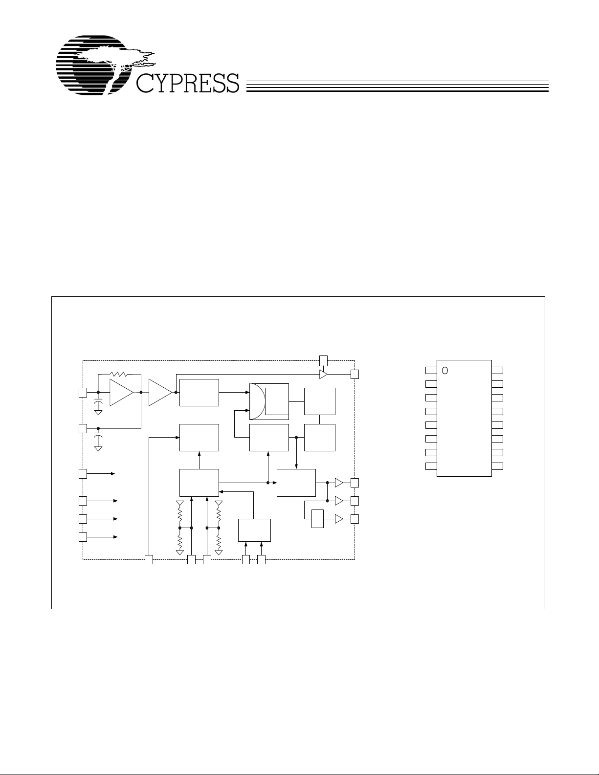
Block Diagram
300K
Xin/
CLK
Xout
VDD
VSS
VSS
VSS
1
16
4
5
11
14
10
SSCC
REFERENCE
MODULA TION
20 K
DIVIDER
CONTROL
INPUT
DECODER
LOGIC
13
12
S0S1
• Center spread modulation
• Low cycle-to cycle jitter
• 16-pin SOIC package
Applications
• High-resolution VGA controllers
• LCD panels and monitors
• Printers and MFPs
Benefits
• Peak EMI reduction by 8 to 16 dB
• Fast time to market
• Cost reduction
Pin Configuration
REFOFF
2
15
14
13
12
11
10
98
XOUT
SSCLK2
VSS
S0
S1
VSS
SSCC
SSCLK1b
3
REFOUT
DIVIDER
&
MUX
Loop
Filter
vco
/2
SSCLK1a
8
915SSCLK1b
SSCLK2
PD
CP
FEEDBACK
DIVIDER
VDDVDD
20 K
RANGE
CONTROL
20 K20 K
VSSVSS
6
7
S3S2
XIN/ CLKIN
SSCLK1a
116
REFOFF
2
REFOUT
3
VDD
4
VSS
5
S2
6
S3
7
CY25566
Cypress Semiconductor Corporation • 3901 North First Street • San Jose • CA 95134 • 408-943-2600
Document #: 38-07429 Rev. *B Revised October 26, 2005
[+] Feedback
Page 2
CY25566
Pin Description
Pin Name Type Description
1 XIN/CLKIN I Clock or Crystal connection input. Refer to Table 1, Table 2, and Table 3 for input
frequency range selection.
2REFOFFIInput pin enables REFOUT clock at pin 3. REFO FF 400K Ω internal pull-up resistor.
Logic “0” enables REFOUT, logic “1” disables REFOUT. Default = disabled.
3REFOUTOBuffered, non-modulated output clock derived from XIN/CLKIN input frequency.
4VDDPPositive power supply. Bypass to ground with 0.1-µF capacitor.
5, 11, 14 VSS G Positive power supply ground.
6S2IVCO range control. Refer to Table 1, Table 2, and Table 3 for detailed programming infor-
7S3IVCO range control. Refer to Table 1, Table 2, and Table 3 for detailed programming infor-
8 SSCLK1a O Modulated clock output . Pins 8 and 9 are identical but separate drivers.
9 SSCLK1b O Modulated clock output . Pins 8 and 9 are identical but separate drivers.
10 SSCC I Spread Spectrum clock control (enable/disable) function. SSCG function is enabled
12 S1 I Tri-level logic input control pin used to select frequency and bandwidth.
13 S0 I Tri-level logic input control pin used to select frequency and bandwidth.
15 SSCLK2 O Modulated output clock. Frequency of SSCLK2 = SSCLK1a/2. BW% of SSCLK2 is equal
16 XOUT O Oscillator output pin connected to crystal. Leave this pin unconnected if an external
There is a 180° phase shift from XIN to REFOUT.
mation. Has 400-KΩ internal pull-up to V
mation. Has 400-KΩ internal pull-up to V
DD
DD
.
.
when input is high and disabled when input is low. Internal 400-KΩ pull-up defaults to
modulation ON.
Frequency/bandwidth selection and tri-level logic programming details. See Figure 2 and
Table 1, Table 2, and Table 3. Pin 8 has internal resistor divider network to V
DD
Frequency/bandwidth selection and tri-level logic programming details. See Figure 2 and
Table 1, Table 2, and Table 3. Pin 8 has internal resistor divider network to V
DD
to BW% of SSCLK1a/b.
clock drives XIN/CLK.
and VSS.
and VSS.
General Description
The Cypress CY25566 is a Spread S pectrum Clock Generator
(SSCG) IC used for the purpose of reducing electromagnetic
interference (EMI) found in today’s high-speed digital
electronic systems.
The CY25566 uses a Cypress-proprietary phase-locked loop
(PLL) and Spread Spectrum Clock (SSC) technology to
synthesize and frequency modulate the input frequency of the
digital clock. By frequency modulating the clock, (SSCLK1a/b
and SSCLK2), the measured EMI at the fundamental and
harmonic frequencies is greatly reduced. The modulated
output frequency is centered on the input frequency.
This reduction in radiated energy can significantly reduce the
cost of complying with regulatory agency requirements and
improve time to market without degrading system performance.
The CY25566 provides four output clocks: SSCLK1a,
SSCLK1b, SSCLK2, and REFOUT. SSCLK1a/b and SSCLK2
are modulated clocks and REFOUT is a buffered copy of the
reference clock or oscillator. The CY25566 frequency and
spread % ranges are selected by programming S0, S1, S2,
and S3 digital inputs. S0 and S1 use three (3) logic states
including High (H), Low (L), and Middle (M) to select one of
nine available frequency and spread % ranges. Refer to
Figure 2 for details on programming three level inputs S0 and
S1. See Table 1, Table 2, and Table 3 for programming details
for S2 and S3.
The CY25566 will operate over a wide range of frequencies
from 25 to 200 MHz. Operation to 200 MHz is possible with the
use of dual drivers at pins 8 and 9. With a wide range of
selectable bandwidths, the CY25566 is a very flexible low-EMI
clock. Modulation can be disabled to provide a four-output
conventional clock.
The CY25566 is available in a 16-pin SOIC (150-mil.) package
with a commercial operating temperature range of 0°C to
70°C.
Output Clock Architecture
The CY25566 provides four separate output clocks: REFOUT ,
SSCLK1a, SSCLK1b, and SSCLK2 for use in a wide variety of
applications. Each clock output is described below in detail.
REFOUT
REFOUT is a 3.3V CMOS level non-modulated inverted copy
of the clock at XIN/CLKIN. As an inverted clock, the output
clock at REFOUT is 180° out of phase with the input clock at
XIN/CLKIN. Placing a high(1) logic state of REFOFF , pin 2, will
disable the REFOUT clock. When REFOUT is disabled,
REFOUT, pin 3 is at a low(0) logic state.
Document #: 38-07429 Rev. *B Page 2 of 9
[+] Feedback
Page 3
CY25566
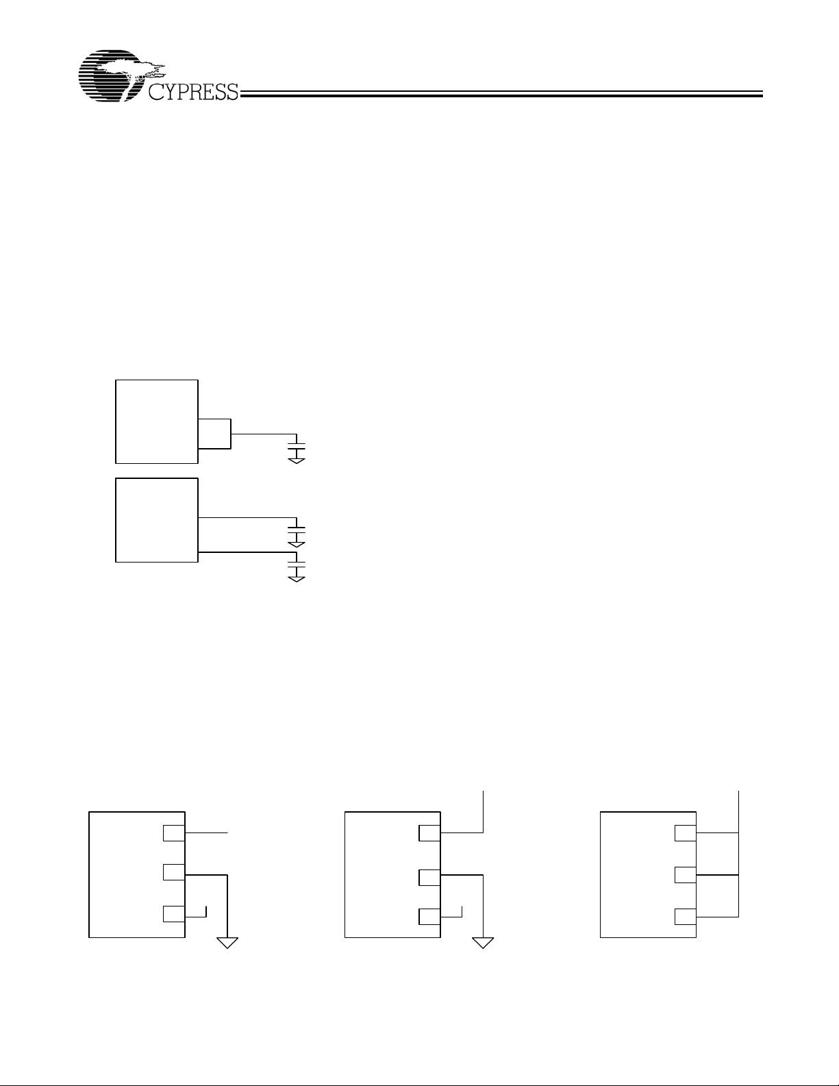
SSCLK1a/b
SSCLK1a and SSCLK1b are spread spectrum clock outputs
used for the purpose of reducing EMI in digital systems.
SSCLK1a and SSCLK1b can be connected in several different
ways to provide flexibility in application designs. Each clock
can drive separate nets with a capacitative load up to 15 pF
each or connected together to provide drive to a single net with
a capacitative load as high as 33 pF. When both clocks are
connected together, the CY25566 is capable of driving 3.3V
CMOS-compatible clocks to frequencies as high as 200 MHz.
If one clock output is not connected to a load, negligible EMI
will be generated at the unused pin because there is no current
being driven. The frequency and bandwidth of SSCLK1a and
SSCLK1b is programmed by the logic states presented to S2
and S3. The frequency multiplication at SSCLK1a and
SSCLK1b is either 1X or 2X, controlled by S2 and S3. The
modulated output clock SSCLK1 is provided at pins 8 and 9
with each pin having separate but identical drivers. Refer to
Figure 1 below .
CY25566
CY25566
9
8
9
8
33 pf.
15 pf.
15 pf.
Figure 1. SSCLK1a/b Driver Configurations
SSCLK2
SCLK2 is a Spread S pectrum Clock with a frequency half that
of the SSCLK1a clock frequency. When SSCLK1a is
programmed to provide a 2.5% modulated clock at 1X times
the reference clock, 40 MHz for example, the frequency of
SSCLK2 will be 20 MHz with a BW of 2.5%. Note that by
programming the frequency of SSCLK1a to 2X, the frequency
of SSCLK2 will be 1X times the reference clock frequency.
CY25566
Control Logic Structures
The CY25566 has six input control pins for programming VCO
range, BW %, Mod ON/OFF and REFOUT ON/OFF. These
programmable control pins are described below.
REFOFF
The output clock REFOUT can be enabled or disabled by
controlling the state of REFOFF. When REFOFF is at a logic
low(0) state, REFOUT is enabled and the reference clock
frequency is present at pin 3. When REFOFF is at a logic high
state (1), REFOUT is disabled and is set to a logic low state
on pin 3. REFOFF has a 400-KW internal pull-up resistor to
V
.
DD
S0 and S1 (Tri-level Inputs)
S0 and S1 are used to program the frequency range and
bandwidth of the modulated output clocks SSCLK1a/b and
SSCLK2. S0 and S1 of the CY25566 are designed to sense
three different analog levels. With this tri-level structure, the
CY25566 is able to detect 9 different logic states. Refer to
tables 5, 6 and 7 for the results of each of these 9 states. The
level of each state is defined as follows:
Logic State “0” is a voltage that is between 0 and 0.15 × V
Logic State “M” is a volt age between 0.4 × V
Logic State “1” is a voltage between 0.85 × V
and 0.6 × VDDV.
DD
and VDD.
DD
DD
Figure 2 illustrates how to program tri-level logic.
S2 and S3
S2 and S3 are used to program the CY25566 into different
frequency ranges and multipliers. The CY25566 operates over
a frequency range of 25 to 200 MHz and a 1X or 2X multipli cation of the reference frequency. S2 and S3 are binary logic
inputs and each has a 400 K W pull-up resistor to V
Table 1, Table 2, and Table 3 for programming details.
DD
. See
SSCC
SSCC is an input control pin that enable s or disables SSCG
modulation of the output clock at SSCLK1a/b and SSCLK2.
Disabling modulation is a method of comparing radiated EMI
in a product with SSCG turned on or off.
The CY25566 can be used as a conventional low jitter multiple
output clock when SSCC is set to low (0). SSCC has a 400-KW
internal pull-up resistor. Logic high (1) = Mo du l a ti on ON, logic
low (0) = Modulation OFF. Default is modulation ON.
VDD VDD
CY25566CY25566
V.
S0 = "M" (N/C)
S1 = "0" (GND)
SSCC = "1"
S0
13
S1
12
VDD
10
S0 = "1" S0 = "1"
S1 = "0" (GND)
SSCC = "1"
S1
12
VDD
10 10
S1 = "1"
SSCC = "1"
S0S0
1313
S1
12
Figure 2.
Document #: 38-07429 Rev. *B Page 3 of 9
[+] Feedback
Page 4

Modulation Rate
CY25566
Spread Spectrum clock generators utilize frequency
modulation (FM) to distribute energy over a specific band of
frequencies. The maximum frequency of the clock (Fmax) and
minimum frequency of the clock (Fmin) determine this band of
frequencies. The time required to transition from Fmin to Fmax
and back to Fmin is the period of the Modulation Rate, Tmod.
Modulation Rates of SSCG clocks are generally referred to in
terms of frequency or Fmod = 1/Tmod.
The input clock frequency, Fin, and the internal divider count,
Cdiv, determine the Modulation Rate. The CY25566 utilizes
two different modulation rate dividers, depending on the range
selected on S2 and S3 digital control inputs. Refer to the
example below.
S3, S2 CDiv Output Frequency
0,0 1 166 1X
0,1 1 166 2X
1,0 2332 1X
1,1 N/A N/A
Example:
Device = CY25566
Fin = 65 MHz
Range = S3 = 0, S2 = 1, S0 = 0
Then: modulation rate = Fmod = 65 MHz/1166 = 55.7 kHz
The CY25566 has three frequency groups to select from. Each
combination of frequency and bandwidth can be selected by
programming the input control lines, S0–S3, to the proper logic
state.
Group 1 is the 1X low-frequency range and operates from 25
to 100 MHz.
Group 2 is the 1X high-frequency range and operates from 50
to 200 MHz.
Group 3 is the 2X low frequency range and operates from 25
to 50 MHz and 50 to 100 MHz output.
Modulation Profile
Figure 3. SSCG Clock, CY25566, 65 MHz
Document #: 38-07429 Rev. *B Page 4 of 9
Spectrum Analyzer
[+] Feedback
Page 5

CY25566
Table 1. Frequency and Bandwidth Selection Chart (Group 1)(Low Frequency (1x) Selection Chart)
25–50 MHz (Low Range)
XIN/CLK
(MHz)
25–35 4.3 3.8 3.4 2.9 2.8
35–40 3.9 3.5 3.1 2.5 2.4
40–45 3.7 3.3 2.8 2.4 2.3
45–50 3.4 3.1 2.6 2.2 2.1
XIN/CLK
(MHz)
50–60 2.9 2.1 1.5 1.2
60–70 2.8 2.0 1.4 1.1
70–80 2.6 1.8 1.3 1.1
80–100 2.4 1.7 1.2 1.0
Table 2. Frequency and Bandwidth Selection Chart (Group 2)(High Frequency (1x) Selection Chart)
XIN/CLK
(MHz)
50–60 4.2 3.8 3.2 2.8 2.7
60–70 4.0 3.6 3.1 2.6 2.5
70–80 3.8 3.4 2.9 2.5 2.4
80–100 3.5 3.1 2.7 2.2 2.1
XIN/CLK
(MHz)
100–120 3.0 2.4 1.6 1.3
120–130 2.7 2.1 1.4 1.1
130–140 2.6 2.0 1.3 1.1
140–150 2.6 2.0 1.3 1.1
150–160 2.5 1.8 1.2 1.0
160–170 2.4 1.8 1.2 1.0
170–180 2.4 1.8 1.2 1.0
180–190 2.3 1.7 1.1 0.9
190–200 2.3 1.6 1.1 0.9
Table 3. Frequency and Bandwidth Selection Chart (Group 3)(Low Frequency (2x) Selection Chart)
XIN/CLK
(MHz)
25–35 50-70 4.0 3.5 3.0 2.6 2.5
35–40 70-80 3.8 3.3 2.9 2.4 2.3
40–45 80-90 3.5 3.1 2.7 2.2 2.1
45–50 90-100 3.3 2.9 2.5 2.1 2.0
S1 = M
S0 = M
S1 = 1
S0 = M
S1 = M
S0 = M
S1 = 1
S0 = M
SSCLK1
(MHz)
S1 = M
S0 = 0
50–100 MHz (High Range)
S1 = 0
S0 = 1
50–100 MHz (Low Range)
S1 = M
S0 =0
100–200 MHz (High Range)
S1 = 0
S0 = 1
25–50 MHz (Low Range, 2X)
S1 = M
S0 = M
S1 = M
S0 = 0
S1 = 1
S0 = 0
S1 = 1
S0 = 1
S1 = 1
S0 = 0
S1 = 1
S0 = 1
S1 = 1
S0 = 0
S1 = 0
S0 = 0
S1 = 0
S0 = 0
S1 = 0
S0 = 0
S1 = M
S0 = 1
S1 = M
S0 = 1
S1 = 0
S0 = M
S1 = 0
S0 = M
S1 = 0
S0 = M
S3
0
S3
0
S3
S3
S3
0
S2
0
S2
0
S2
1
0
S2
1
0
S2
1
Document #: 38-07429 Rev. *B Page 5 of 9
[+] Feedback
Page 6

Application Schematic
CY25566
In this example, the CY25566 is being driven by a 75 -MHz
reference clock.
S0 = 0 and S1 = 0 are programmed to select a BW of 2.5%.
(Refer to Table 1 and 2.)
S2 = 0 and S3 = 1 are programmed to select the Group 2
range.
VDD
0.1 uF
75 MHz Clock source
VDD
1
XIN/CLKIN
16
XOUT
2
REFOFF
10
SSCC
7
S3
6
S2
12
S1
13
S0
51114
V
= 3.30 VDC.
DD
SSCLK1a = 75 MHz @ 2.5% center spread modulation.
SSCLK1b = 75 MHz @ 2.5% center spread modulation.
SSCLK 2 = 37.5 MHz @ 2.5% center spread modulation.
REFOUT = 37.5 MHz non-modulated clock.
4
VDD
REFOUT
SSCLK2
CY25566
SSCLK1a
SSCLK1b
VSS VSS VSS
3
15
8
9
REFOUT
SSCLK2
SSCLK1a
SSCLK1b
Figure 4. Application Schematic
Document #: 38-07429 Rev. *B Page 6 of 9
[+] Feedback
Page 7
CY25566
Absolute Maximum Ratings
[1, 2]
Supply Voltage (VDD: .......................................................+6V
Operating Temperature:......................................0°C to 70°C
Storage Temperature..................................–65°C to +150°C
Table 4. DC Electrical Characteristics VDD = 3.3V, Temp. = 25°C, unless otherwise noted
Parameter Description Conditions Min. Typ. Max. Unit
V
DD
V
INH
V
INM
V
INL
V
OH1
V
OH2
V
OL1
V
OL2
C
in1
C
in2
C
in2
I
DD1
I
DD1
I
DD2
I
DD2
Table 5. Electrical Timing Characteristics V
Duty@1.5V
Power Supply Range ±10 % 2.97 3.3 3.63 V
Input High Voltage S0 and S1 only. 0.85V
Input Middle Voltage S0 and S1 only. 0.40V
DD
DD
Input Low Voltage S0 and S1 only. 0.0 0.0 0.15V
V
DD
0.50V
DD
V
DD
0.60V
DD
DD
V
V
V
Output High Voltage IOH = 6 ma, SSCLKa 2.4 V
Output High Voltage IOH = 20 ma, SSCLKb 2.0 V
Output Low Voltage IOH = 6 ma, SSCLKa 0.4 V
Output Low Voltage IOH = 20 ma, SSCLKb 1.2 V
Input Capacitance Xin/CLK (Pin 1) 3 4 5 pF
Input Capacitance Xout (Pin 8) 6 8 10 pF
Input Capacitance All input pins except 1. 3 4 5 pF
Power Supply Current FIN = 40 MHz,15 pF@all outputs 27 32 mA
Power Supply Current FIN = 40 MHz, No Load 21 28 mA
Power Supply Current FIN = 165 MHz,15 pF@all outputs 68 80 mA
Power Supply Current FIN = 165 MHz, No Load 48 60 mA
= 3.3V , T = 25°C and CL = 15 pF , unless otherwise noted. Rise/Fall @ 0.4–2.4V ,
DD
Parameter Description Conditions Min. Typ. Max Unit
I
CLKFR
t
RISE(a)
t
FALL(a)
t
RISE(a+b)
t
FALL(a+b)
t
RISE(a+b)
t
FALL(a+b)
t
RISE(REF)
t
FALL(REF)
D
TYin
D
TYout
C
CJ1
C
CJ2
Input Clock Frequency Range Non-crystal, 3.0V Pk–Pk ext. source 25 200 MHz
Clock Rise Time SSCLK1a or SSCLK1b, Freq = 100 MHz 1.0 1.3 1.6 ns
Clock Fall Time SSCLK1a or SSCLK1b, Freq = 100 MHz 1.0 1.3 1.6 ns
Clock Rise Time SSCLK1(a+b), CL = 33 pF, 100 MHz 1.2 1.5 1.8 ns
Clock Fall Time SSCLK1(a+b), CL = 33 pF, 100 MHz 1.2 1.5 1.8 ns
Clock Rise Time SSCLK1(a+b), CL = 33 pF, 200 MHz 1.1 1.4 1.7 ns
Clock Fall Time SSCLK1(a+b), CL = 33 pF, 200 MHz 1.1 1.4 1.7 ns
Clock Rise Time REFOUT, Pin 3, CL = 15 pF, 50 MHz 1.0 1.3 1.6 ns
Clock Fall Time REFOUT, Pin 3, CL = 15 pF, 50 MHz 1.0 1.3 1.6 ns
Input Clock Duty Cycle XIN/CLK (Pin) 30 50 70 %
Output Clock Duty Cycle SSCLK1a/b (Pin 8 and 9) 45 50 55 %
Cycle-to-Cycle Jitter F = 100 MHz, SSCLK1a/b CL = 33 pF 300 400 ps
Cycle-to-Cycle Jitter F = 200 MHz, SSCLK1a/b CL = 33 pF 500 600 ps
REFOUT Refout Frequency Range CL = 15 pF 25 108 MHz
Note:
1. Operation at any Absolute Maximum Rating is not implied.
2. Single Power Supply: The voltage on any input or I/O pin cannot exceed the power pin during power-up.
Document #: 38-07429 Rev. *B Page 7 of 9
[+] Feedback
Page 8

CY25566
Ordering Information
Part Number Package Type Product Flow
CY25566SC 16-pin SOIC Commercial, 0° to 70°C
CY25566SCT 16-pin SOIC–Tape and Reel Commercial, 0° to 70°C
Package Drawing and Dimensions
16 Lead (150 Mil) SOIC
16-Lead (150-Mil) SOIC S16.15
18
916
0.386[9.804]
0.393[9.982]
0.050[1.270]
BSC
0.0138[0.350]
0.0192[0.487]
PIN 1 ID
0.150[3.810]
0.157[3.987]
0.061[1.549]
0.068[1.727]
0.004[0.102]
0.0098[0.249]
0.230[5.842]
0.244[6.197]
SEATING PLANE
0.004[0.102]
DIMENSIONS IN INCHES[MM] MIN.
REFERENCE JEDEC MS-012
PACKAGE WEIGHT 0.15gms
S16.15 STANDARD PKG.
SZ16.15 LEAD FREE PKG.
0°~8°
0.016[0.406]
0.035[0.889]
PART #
0.010[0.254]
0.016[0.406]
MAX.
X 45°
0.0075[0.190]
0.0098[0.249]
51-85068-*B
All product and company names mentioned in this document are the trademarks of their respective holders.
Document #: 38-07429 Rev. *B Page 8 of 9
© Cypress Semiconductor Corporation, 2002. The information contained herein is subject to change without notice. Cypress Semiconductor Corporation assumes no responsibility for the use
of any circuitry other than circui try embodied in a Cypress Semicond uctor product. Nor d oes it convey or imply any licen se under patent or other rights. Cypress Semiconductor does not authorize
its products for use as critical components in life-support systems where a malfunction or failure may reasonably be expected to result in significant injury to the user. The inclusion of Cypress
Semiconductor products in life-support systems application implies that the manufacturer assumes all risk of such use and in doing so ind emnifie s Cypress Semicondu ctor ag ainst all charges.
[+] Feedback
Page 9

CY25566
Document Title:CY25566 Spread Spectrum Clock Generator
Document Number: 38-07429
Rev. ECN No.
** 115771 07/01/02 OXC New Data Sheet
*A 122705 12/30/02 RBI Added power up requirements to maximum ratings information.
*B 404070 See ECN RGL Minor Change: Typo error on table 1, column 2 , S0 = 0 (not M)
Issue
Date
Orig. of
Change
Description of Change
Document #: 38-07429 Rev. *B Page 9 of 9
[+] Feedback
 Loading...