

CY23S08
3.3V Zero Delay Buffer
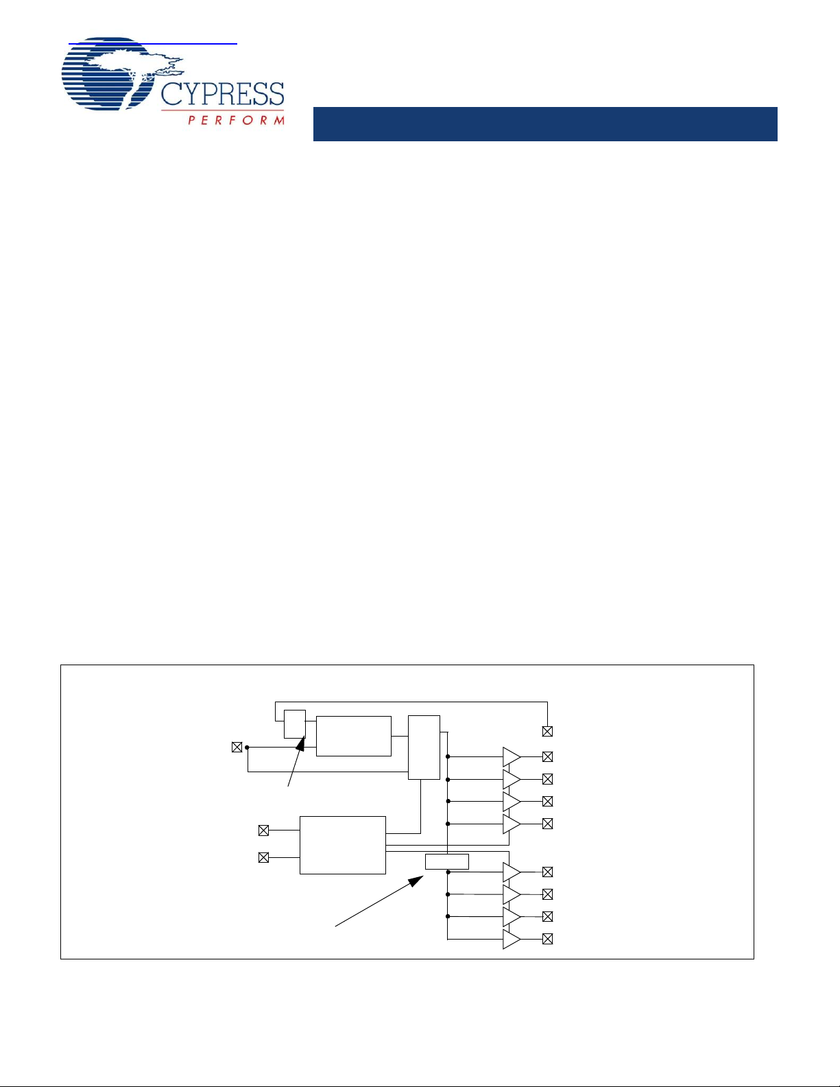
Logic Block Diagram
REF
CLKA1
CLKA2
CLKA3
CLKA4
FBK
PLL
MUX
Select Input
Decoding
S2
S1
CLKB1
CLKB2
CLKB3
CLKB4
/2
Extra Divider (–2, –2H, –3)
/2
Extra Divider (–3, –4)
查询CY23S08SI-1供应商
Features
■ Zero input-output propagation delay, adjustable by capacitive
load on FBK input
■ Multiple configurations, see Table 3 on page 3
■ Multiple low-skew outputs
❐ 45 ps typical output-output skew(–1)
❐ Two banks of four outputs, three-stateable by two select in-
puts
■ 10 MHz to 133 MHz operating range
■ 65 ps typical cycle-cycle jitter (–1, –1H)
■ Advanced 0.65μ CMOS technology
■ Space saving 16-pin 150-mil SOIC/TSSOP packages
■ 3.3V operation
■ Spread Aware™
Functional Description
The CY23S08 is a 3.3V zero delay buffer designed to distribute
high speed clocks in PC, workstation, datacom, telecom, and
other high performance applications.
The part has an on-chip PLL which locks to an input clock
presented on the REF pin. The PLL feedback must be driven into
the FBK pin, and can be obtained from one of the outputs. The
input-to-output propagation delay is guaranteed to be less th an
350 ps, and output-to-output skew is guaranteed to be less than
250 ps.
The CY23S08 has two banks of four outputs each, which can be
controlled by the Select inputs as shown in Table 2 on page 3. If
all output clocks are not required, Bank B can be three-stated.
The select inputs also allow the input clock to be directly applied
to the output for chip and system testing purposes.
The CY23S08 PLL enters a power down state when there are no
rising edges on the REF input. In this mode, all outputs are
three-stated and the PLL is turned off, resulting in less than
50 μA of current draw. The PLL shuts down in two additional
cases as shown in Table 2 on page 3.
Multiple CY23S08 devices can accept the same input clock and
distribute it in a system. In this case, the skew between the
outputs of two devices is guaranteed to be less than 700 ps.
The CY23S08 is available in five different configurations, as
shown in Ta ble 3 on page 3. The CY23S08–1 is the base part,
where the output frequencies equal the reference if there is no
counter in the feedback path. The CY23S08–1H is the high-drive
version of the –1, and rise and fall times on this device are much
faster.
The CY23S08–2 enables the user to obtain 2X and 1X
frequencies on each output bank. The exact configuration and
output frequencies depends on which output drives the feedback
pin. The CY23S08–2H is the high-drive version of the –2, and
rise and fall times on this device are much faster.
The CY23S08–3 enables the user to obtain 4X and 2X
frequencies on the outputs.
The CY23S08–4 enables the user to obtain 2X clocks on all
outputs. Thus, the part is extremely versatile, and can be used
in a variety of applications.
Cypress Semiconductor Corporation • 198 Champion Court • San Jose, CA 95134-1709 • 408-943-2600
Document #: 38-07265 Rev. *G Revised September 05, 2007
[+] Feedback
CY23S08
Pinouts
9
16
FBK
CLKA4
CLKA3
V
DD
GND
CLKB4
CLKB3
S1
1
2
3
4
5
6
7
8
10
11
12
13
14
15
REF
CLKA1
CLKA2
V
DD
GND
CLKB1
CLKB2
S2
Top View
SOIC
Notes
1. Output phase is indeterminant (0° or 180° from input clock). If phase integrity is required, use the CY23S08–2.
2. Weak pull down.
3. Weak pull down on all outputs.
4. Weak pull ups on these inputs.
Figure 1. Pin Diagram - 16 Pin SOIC Package
Table 1. Pin Definition - 16 Pin SOIC Package
Pin Signal Description
DD
DD
[2]
[3]
[3]
Input reference frequency, 5V tolerant input
Clock output, Bank A
Clock output, Bank A
3.3V supply
[3]
[3]
[4]
[4]
[3]
[3]
Clock output, Bank B
Clock output, Bank B
Select input, bit 2
Select input, bit 1
Clock output, Bank B
Clock output, Bank B
3.3V supply
[3]
[3]
Clock output, Bank A
Clock output, Bank A
1REF
2 CLKA1
3 CLKA2
4V
5 GND Ground
6 CLKB1
7 CLKB2
8S2
9S1
10 CLKB3
1 1 CLKB4
12 GND Ground
13 V
14 CLKA3
15 CLKA4
16 FBK PLL feedback input
Document #: 38-07265 Rev. *G Page 2 of 10
[+] Feedback
CY23S08
Table 2. Select Input Decoding
S2 S1 CLOCK A1–A4 CLOCK B1–B4 Output Source PLL Shutdown
0 0 Three-State Three-S tate PLL Y
0 1 Driven Three-State PLL N
1 0 Driven Driven Reference Y
1 1 Driven Driven PLL N
Table 3. Available CY23S08 Configurations
Device Feedback From Bank A Frequency Ba nk B Frequency
CY23S08–1 Bank A or Bank B Reference Reference
CY23S08–1H Bank A or Bank B Reference Reference
CY23S08–2 Bank A Reference Reference/2
CY23S08–2H Bank A Reference Reference/2
CY23S08–2 Bank B 2 X Reference Reference
CY23S08–2H Bank B 2 X Reference Reference
CY23S08–3 Bank A 2 X Reference Reference or Reference
CY23S08–3 Bank B 4 X Reference 2 X Reference
CY23S08–4 Bank A or Bank B 2 X Reference 2 X Reference
[1]
Spread Aware
Many systems being designed now utilize a technology calle d Spread Spectrum Frequency Timing Generation. Cypress has been
one of the pioneers of SSFTG development, and we designed this product so as not to filter off the Spread Spectrum feature of the
Reference input, assuming it exists. When a zero delay buffer is not designed to pass the SS feature through, the result is a significant
amount of tracking skew which may cause problems in systems requiring synchronization.
For more details on Spread Spectrum timing technology, please see Cypress’s application note EMI Suppression Techniques with
Spread Spectrum Frequency Timing Generator (SSFTG) ICs.
Document #: 38-07265 Rev. *G Page 3 of 10
[+] Feedback

CY23S08
Maximum Ratings
Supply Voltage to Ground Potential................–0.5V to +7.0V
DC Input Voltage (Except Ref) ..............–0.5V to V
+ 0.5V
DD
DC Input Voltage REF...........................................–0.5 to 7V
Storage Temperature ................................. –65°C to +150°C
Max. Soldering Temperature (10 sec.)....................... 260°C
Junction Temperature................................................. 150°C
Static Discharge Voltage
(per MIL-STD-883, Method 3015) .............................>2000V
Operating Conditions for CY23S08SC-XX Commercial Temperature Devices
Parameter
V
DD
T
A
C
L
C
IN
[5]
Description Min Max Unit
Supply Voltage 3.0 3.6 V
Operating Temperature (Ambient Temperature) 0 70 °C
Load Capacitance, below 100 MHz — 30 pF
Load Capacitance, from 100 MHz to 133 MHz — 15 pF
Input Capacitance
[6]
—7 pF
Electrical Characteristics for CY23S08SC-XX Commercial Temperature Devices
Parameter Description Test Conditions Min Max Unit
V
IL
V
IH
I
IL
I
IH
V
OL
V
OH
IDD (PD mode) Power down Supply Current REF = 0 MHz — 12.0 μA
I
DD
Input LOW Voltage — 0.8 V
Input HIGH Voltage 2.0 — V
Input LOW Current V
Input HIGH Current VIN = V
Output LOW Voltage
Output HIGH Voltage
[7]
[7]
Supply Current Unloaded outputs, 100-MHz REF,
= 0V — 50.0 μA
IN
DD
IOL = 8 mA (–1, –2, –3, –4)
= 12 mA (-1H, -2H)
I
OL
IOH = –8 mA (–1, –2, –3, –4)
= –12 mA (–1H, –2H)
I
OH
— 100.0 μA
—0.4 V
2.4 — V
— 45.0 mA
Select inputs at V
or GND
DD
— 70.0
(–1H, –2H)
Unloaded outputs, 66-MHz REF
— 32.0 mA
(–1,–2,–3,–4)
Unloaded outputs, 33-MHz REF
— 18.0 mA
(–1,–2,–3,–4)
mA
Switching Characteristics for CY23S08SC-XX Commercial Temperature Devices
Parameter
t1 Output Frequency 30-pF load, –1, –1H, –2, –3 devices 10 — 100 MHz
t1 Output Frequency 30-pF load, –4 devices 15 — 100 MHz
t1 Output Frequency 20-pF load, –1H device 10 — 133.3 MHz
t1 Output Frequency 15- pF load, –1, –2, –3, devices 10 — 140.0 MHz
t1 Output Frequency 15-pF load, –4 devices 15 — 140.0 MHz
Notes
5. Multiple Supplies: The voltage on any input or IO pin cannot exceed the power pin during power up. Power supply sequencing is NOT required.
6. Applies to both Ref Clock and FBK.
7. Parameter is guaranteed by design and characterization. Not 100% tested in production.
8. All parameters are specified with loaded outputs.
Document #: 38-07265 Rev. *G Page 4 of 10
[8]
Duty Cycle
Name Test Conditions Min Typ. Max Unit
[7]
= t2 ÷ t
(–1,–2,–3,–4,–1H, -2H)
Duty Cycle
[7]
= t2 ÷ t
(–1,–2,–3,–4,–1H, -2H)
1
1
Measured at V
30-pF load
Measured at V
15-pF load
DD
DD
/2, F
/2, F
= 66.66 MHz
OUT
<66.66 MHz
OUT
40.0 50.0 60.0 %
45.0 50.0 55.0 %
[+] Feedback

CY23S08
Switching Characteristics for CY23S08SC-XX Commercial Temperature Devices (continued)
Parameter
t3 Rise Time
t3 Rise Time
t3 Rise Time
t
4
t
4
t
4
t
5
t
6
t
7
t
8
t
J
t
J
t
LOCK
[8]
Fall Time
Fall Time
Fall Time
Output to Output Skew on
same Bank (–1)
Name Test Conditions Min Typ. Max Unit
[7]
(–1, –2, –3, –4) Measured between 0.8V and 2.0V, 30-pF
[7]
(–1, –2, –3, –4) Measured between 0.8V and 2.0V, 15-pF
[7]
(–1H, -2H) Measured between 0.8V and 2.0V, 30-pF
[7]
(–1, –2, –3, –4) Measured between 0.8V and 2.0V, 30-pF
[7]
(–1, –2, –3, –4) Measured between 0.8V and 2.0V, 15-pF
[7]
(–1H, 2H) Measured between 0.8V and 2.0V, 30-pF
[7]
Output to Output Skew on
same Bank
(–1H,–2,–2H,–3)
Output to Output Skew on
same Bank (–4)
[7]
[7]
Output to Output Skew
(–1H, -2H)
Output Bank A to Output
Bank B Skew (–1,–2, –3)
Output Bank A to Output
Bank B Skew (–4)
Output Bank A to Output
Bank B Skew (–1H)
Delay, REF Rising Edge to
FBK Rising Edge
[7]
Device to Device Skew
Output Slew Rate
[7]
Cycle to Cycle Jitter
(–1, –1H)
Cycle to Cycle Jitter
(–2)
Cycle to Cycle Jitter
(–2)
Cycle to Cycle Jitter
(–3,–4)
PLL Lock Time
[7]
[7]
[7]
[7]
[7]
load
— — 2.20 ns
— — 1.50 ns
load
— — 1.50 ns
load
— — 2.20 ns
load
— — 1.50 ns
load
— — 1.25 ns
load
All outputs equally loaded 45 200 ps
All outputs equally loaded — 105 150 ps
All outputs equally loaded — 70 100 ps
All outputs equally loaded — — 20 0 ps
All outputs equally loaded — — 30 0 ps
All outputs equally loaded — — 21 5 ps
All outputs equally loaded — — 25 0 ps
Measured at VDD/2 –250 — +275 ps
[7]
Measured at VDD/2 on the FBK pins of
——700ps
devices
Measured between 0.8V and 2.0V on –1H,
1— V/ns
–2H device using Test Circuit #2
Measured at 66.67 MHz, loaded outputs, 15,
—65125ps
30-pF loads: 133 MHz, 15-pF load
Measured at 66.67 MHz, loaded outputs,
—85300ps
15-pF load
Measured at 66.67 MHz, loaded outputs,
——400ps
30-pF load
Measured at 66.67 MHz, loaded outputs
——200ps
15, 30-pF loads
Stable power supply, valid clocks presented
——1.0ms
on REF and FBK pins
Document #: 38-07265 Rev. *G Page 5 of 10
[+] Feedback

CY23S08
Switching Waveforms
t
1
t
2
1.4V 1.4V 1.4V
OUTPUT
t
3
3.3V
0V
0.8V
2.0V 2.0V
0.8V
t
4
1.4V
t
5
OUTPUT
OUTPUT
1.4V
VDD/2
t
6
INPUT
FBK
V
DD
/2
VDD/2
V
DD
/2
t
7
FBK, Device 1
FBK, Device 2
Figure 2. Duty Cycle Timing
Figure 3. All Outputs Rise/Fall Time
Figure 4. Output-Output Skew
Figure 5. Input-Output Propagation Delay
Figure 6. Device-Device Skew
Document #: 38-07265 Rev. *G Page 6 of 10
[+] Feedback

CY23S08
Test Circuits
0.1 μF
V
DD
0.1 μF
V
DD
CLK
OUT
C
LOAD
OUTPUTS
GND
GND
Test Circuit for all parameters except t
8
V
DD
0.1 μF
V
DD
CLK
out
10 pF
OUTPUTS
GND
GND
1 KΩ
1 KΩ
0.1 μF
Test Circuit for t8, Output slew rate on –1H device
Te st Circuit # 2
Figure 7. Test Circuit #1
Figure 8. Test Circuit #2
Document #: 38-07265 Rev. *G Page 7 of 10
[+] Feedback

CY23S08
Ordering Information
Ordering Code Package Type Operating Range Status
CY23S08SC–1 16-pin 150-mil SOIC Commercial Obsolete
CY23S08SC–1T 16-pin 150-mil SOIC–Tape and Reel Commercial Obsolete
CY23S08SI–1 16-pin 150-mil SOIC Industrial Obsolete
CY23S08SI–1T 16-pin 150-mil SOIC–Tape and Reel Industrial Obsolete
CY23S08SC–1H 16-pin 150-mil SOIC Commercial Obsolete
CY23S08SC–1HT 16-pin 150-mil SOIC–Tape and Reel Commercial Obsolete
CY23S08SI–1H 16-pin 150-mil SOIC Industrial Not for new design
CY23S08SI–1HT 16-pin 150-mil SOIC–Tape and Reel Industrial Not for new design
CY23S08ZC–1H 16-pin 150-mil TSSOP Commercial Not for new design
CY23S08ZC–1HT 16-pin 150-mil TSSOP–Tape and Reel Commercial Obsolete
CY23S08SC–2 16-pin 150-mil SOIC Commercial Not for new design
CY23S08SC–2T 16-pin 150-mil SOIC–Tape and Reel Commercial Not for new design
CY23S08SI–2 16-pin 150-mil SOIC Industrial Not for new design
CY23S08SI–2T 16-pin 150-mil SOIC–Tape and Reel Industrial Not for new design
CY23S08SC–2H 16-pin 150-mil SOIC Commercial Obsolete
CY23S08SC–2HT 16-pin 150-mil SOIC–Tape and Reel Commercial Active
CY23S08SC–3 16-pin 150-mil SOIC Commercial Obsolete
CY23S08SC–3T 16-pin 150-mil SOIC–Tape and Reel Commercial Obsolete
CY23S08SC–4 16-pin 150-mil SOIC Commercial Obsolete
CY23S08SC–4T 16-pin 150-mil SOIC–Tape and Reel Commercial Obsolete
CY23S08SI–4 16-pin 150-mil SOIC Industrial Obsolete
CY23S08SI–4T 16-pin 150-mil SOIC–Tape and Reel Industrial Obsolete
Pb-free
CY23S08SXC–1 16-pin 150-mil SOIC Commercial Active
CY23S08SXC–1T 16-pin 150-mil SOIC–Tape and Reel Commercial Active
CY23S08SXI–1H 16-pin 150-mil SOIC Industrial Active
CY23S08SXI–1HT 16-pin 150-mil SOIC–Tape and Reel Industrial Active
CY23S08ZXC-1H 16-pin 150-mil TSSOP Commercial Active
CY23S08SXC–2 16-pin 150-mil SOIC Commercial Active
CY23S08SXC–2T 16-pin 150-mil SOIC–Tape and Reel Commercial Active
CY23S08SXC–2H 16-pin 150-mil SOIC Commercial Active
CY23S08SXC–2HT 16-pin 150-mil SOIC–Tape and Reel Commercial Active
CY23S08SXI–2 16-pin 150-mil SOIC Industrial Active
CY23S08SXI–2T 16-pin 150-mil SOIC–Tape and Reel Industrial Active
CY23S08SXC-4 16-pin 150-mil SOIC Commercial Active
CY23S08SXC-4T 16-pin 150-mil SOIC–Tape and Reel Commercial Active
CY23S08SXI-4 16-pin 150-mil SOIC Industrial Active
CY23S08SXI-4T 16-pin 150-mil SOIC–Tape and Reel Industrial Active
Document #: 38-07265 Rev. *G Page 8 of 10
[+] Feedback

CY23S08
Package Drawings and Dimensions
PIN 1 ID
0°~8°
18
916
SEATING PLANE
0.230[5.842]
0.244[6.197]
0.157[3.987]
0.150[3.810]
0.386[9.804]
0.393[9.982]
0.050[1.270]
BSC
0.061[1.549]
0.068[1.727]
0.004[0.102]
0.0098[0.249]
0.0138[0.350]
0.0192[0.487]
0.016[0.406]
0.035[0.889]
0.0075[0.190]
0.0098[0.249]
DIMENSIONS IN INCHES[MM] MIN.
MAX.
0.016[0.406]
0.010[0.254]
X 45°
0.004[0.102]
REFERENCE JEDEC MS-012
PART #
S16.15 STANDARD PKG.
SZ16.15 LEAD FREE PKG.
PACKAGE WEIGHT 0.15gms
51-85068-*B
4.90[0.193]
1.10[0.043] MAX.
0.65[0.025]
0.20[0.008]
0.05[0.002]
16
PIN 1 ID
6.50[0.256]
SEATING
PLANE
1
0.076[0.003]
6.25[0.246]
4.50[0.177]
4.30[0.169]
BSC.
5.10[0.200]
0.15[0.006]
0.19[0.007]
0.30[0.012]
0.09[[0.003]
BSC
0.25[0.010]
0°-8°
0.70[0.027]
0.50[0.020]
0.95[0.037]
0.85[0.033]
PLANE
GAUGE
51-85091-*A
Figure 9. 16-Lead (150-Mil) SOIC S16
Figure 10. 16-Lead Thin Shrunk Small Outline Package (4.40 MM Body) Z16
Document #: 38-07265 Rev. *G Page 9 of 10
[+] Feedback

CY23S08
Document History Page
Document Title: CY23S08 3.3V Zero Delay Buffer
Document Number: 38-07265
REV. ECN NO. Issue Date
** 1 10530 12/02/01 SZV Change from Spec number: 38-01107 to 38-07265
*A 122863 12/20/02 RBI Added power up requirements to operating conditions information.
*B 130951 11/26/03 RGL Corrected the Switching Characteristics parameters to reflect the W152 device
*C 204201 See ECN RGL Corrected the Block Diagram
*D 231100 See ECN RGL Fixed Typo in table 2.
*E 378878 See ECN RGL Added Industrial Temp and Pb Free Devices
*F 391564 See ECN RGL Changed output-to-output skew typical value from 90ps to 45ps
*G 1442823 See ECN WWZ/AESA Updated ordering info with status update. Added new Pb-free part numbers.
Orig. of
Change
Description of Change
and new characterization.
Added typical char data
Removed “Preliminary”
Added cycle-to-cycle jitter (-2) typical value of 85ps
© Cypress Semiconductor Corporation, 2001- 2007. The infor mation cont ain ed herein is subj ect to change wi thout notice. C ypress Semiconductor Corporation assumes no responsibility for the use of
any circuitry other than circuitry embodied in a Cypress product. Nor does it convey or imply any license under patent or other rights. Cypress products are not warranted nor int e nded to be used fo r
medical, life support, life saving, critica l contr o l or safety applications, unless pursuant to an express wr itte n agreement with Cypress. Furthermore, Cypress does not authoriz e it s pr o ducts for use as
critical components in life-support systems where a malfunction or fa ilure may reasonably be expe cted to result in significa nt injury to the us er . The inclu sion of Cypress p roducts in life -support systems
application implies that the manufacturer assumes all risk of such use and in doing so indemnifies Cypress against all charges.
Any Source Code (software and/or firmware) is owned by Cypress Semiconductor Corporation (Cypress) and is protected by and subject to worldwide patent protection (United States and foreign),
United States copyright laws and international treaty provisions. Cypress hereby gr ant s to l icense e a pers onal, no n-exclu sive , non-tr ansfer able license to copy, use, modify, create derivative works of,
and compile the Cypress Source Code and derivative works for the sole purpose of creating custom software and or firmware in support of licensee product to be used only in conjunctio n with a Cypress
integrated circuit as specified in the ap plicable agreem ent. Any reprod uction, modificatio n, translation, co mpilation, or repr esentation of this Source Co de except as speci fied above is pro hibited with out
the express written permission of Cypress.
Disclaimer: CYPRESS MAKES NO WARRANTY OF ANY KIND, EXPRESS OR IMPLIED, WITH REGARD TO THIS MATERIAL, INCLUDING, BUT NOT LIMITED TO, THE IMPLIED WARRANTIES
OF MERCHANTABILITY AND FITNESS FOR A PARTICULAR PURPOSE. Cypress reserves the right to make changes without further notice to the materials described herein. Cypres s does not
assume any liability arising out of the applic ation or use o f any pr oduct or circ uit de scribed herein . Cypr ess does n ot author ize its p roducts fo r use as critical compon ents in life-su pport systems whe re
a malfunction or failure may reason ably be expected to result in significant injury to the user. The inclusion of Cypress’ product in a life-support systems application implies that the manufacturer
assumes all risk of such use and in doing so indemnifies Cypress against all charges.
Use may be limited by and subject to the applicable Cypress software license agreement.
Document #: 38-07265 Rev. *G Revised September 05, 2007 Page 10 of 10
Spread Aware is a trademark of Cypress Semiconductor. All products and company names mentioned in this document may be the trademarks of their respective holders.
[+] Feedback
 Loading...