

Page 1

CY2048WAF
Flash Programmable Capacitor Tuning Array Die
for Crystal Oscillator(XO)
Features
• Flash-programmable capacitor tuning array for low
ppm initial frequency clock output
• Low clock output jitter
— 4 ps typ. RMS period jitter
— ±30 ps typ. peak-to-peak period jitter
• Flash-programmable dividers
• Two-pin programming interface
• On-chip os cillator runs from 10–48-MHz crystal
• Five selectable post-divide options, using reference
oscillator output
• Programmable asynchronous or synchronous OE and
PWR_DWN modes
• 2.7V to 3.6V operation
• Controlled rise and fall times and output slew rate
Block Diagram
PD#/OE
(SDATA/VPP)
XIN
XOUT
CRYSTAL
OSCILLATOR
Benefits
• Enables fine-tuning of output clock frequency by
adjusting C
• Allows multiple programming opportunities to correct
errors, and control excess inventory
• Enables programming of output frequency after
packaging
• PPM clock output err or can be adjusted in package
• Provides flexibility in output configurations and testing
• Enables low-power operation or output enable function
• Provides flexibility for system applications through
selectable instantaneous or synchronous change in
outputs
• Enables encapsulation in small-size, surface-mount
packages
of the crystal
Load
CONFIGURATION
/ 1, 2, 4, 8, 16
VDD
VSS
OUT
(SCL)
Die Pad Description
Horizontal Scribe
1
2
3
4
VDD
XOUT
XIN
PD#/OE
Y (max)
7C80330A
X(max)
OUT
VSS
6
5
Vertical
Scribe
die#/rev
Cypress Semiconductor Corporation • 3901 North First Street • San Jose, CA 95134 • 408-943-2600
Document #: 38-07738 Rev. *A Revised December 12, 2005
Notes:
X(max): 980 µm, Y(max): 988 µm
Scribe: X = 70 µm, Y = 86 µm
Bond pad opening: 85 µm x 85 µm
Pad pitch: 175 µm (min.)
Wafer thickness: 11 mils (T yp.)
[+] Feedback
Page 2
CY2048WAF
Die Pad Summary (Pad coordinates are referenced from the center of the die (X = 0, Y = 0))
Name Pad Number Description X coordinate (µm) Y coordinate (µm)
VDD 1 Voltage Supply –360.8 353.7
XOUT 2 Oscillator Drain –360.8 134.1
XIN 3 Oscillator Gate –360.8 –42.6
PD#/OE 4 Programmable power-down or output enable pin –360.8 –275.9
VPP High voltage for programming NV memory
SDATA Serial data pin used for programming in test mode
OUT 6 Clock output 360.0 353.7
SCL Serial clock for programming in te st mode
VSS 5 Ground 360.0 –354.5
Document #: 38-07738 Rev. *A Page 2 of 7
[+] Feedback
Page 3
CY2048WAF
Absolute Maximum Conditions
(Above which the useful life may be impaired.
For user guidelines, not tested.)
Supply Voltage (V
DC Input Voltage......................................–0.5V to V
Crystal Specifications
).................................. ......–0.5 to +7.0V
DD
[1]
DD
+ 0.5
Output Short Circuit Current.....................................± 50 mA
Storage Temperature (Non-condensing) .... –55°C to +125°C
Junction Temperature................................ –40°C to +125°C
Data Retention @ Tj = 125°C................................> 10 years
ESD (Human Body Model) MIL-STD-883.................> 2000V
Parameter Description Comments Min. Typ. Max. Unit
F
R
R
C
C
NOM
1
3/R1
0
1
Nominal crystal frequency Fundamental mode, AT cut 10 – 48 MHz
Equivalent series resistance (ESR) Fundamental mode – – 40 Ω
Ratio of third overtone mode ESR to
fundamental mode ESR
Ratio used because typical R1 values are
much less than the maximum spec
4.5 – – –
Crystal shunt capacitance – – 5 pF
Crystal motional capacitance 2 – – fF
Operating Conditions
Parameter Description Min. Typ. Max. Unit
V
DD
T
J
C
XIN
C
XOUT
C
L
C
OUT
t
RAMP
T
S
Operating Voltage 2.7 – 3.6 V
Junction Temperature –40 – 125 °C
Capacitance XIN, all tuning caps OFF – 10 – pF
Capacitance XOUT, all tuning caps OFF – 10 – pF
All tuning Caps OFF 4 5 6 pF
All tuning Caps ON 9.2 10 11.4 pF
Output Load Capacitance – – 15 pF
Power-up time for VDD to reach minimum specified
0.05 – 500 ms
voltage (power ramps must be monotonic)
Start up time, 90% VDD to valid frequency on output – – 10 ms
DC Electrical Specifications TJ = –40 to 125°C over the operating range
Parameter Description Condition Min. Typ. Max. Unit
V
IL
V
IH
V
OL
V
OH
I
IL
I
IH
I
OZL
I
OZH
I
DD
I
PD
R
UP
R
DN
C
IN
R
F
Note:
1. Not 100% tested.
Input Low Voltage CMOS Levels – – 20 %VDD
Input High Voltage CMOS Levels 80 – – %VDD
Output Low Voltage VDD = 2.7V–3.6V, IOL = 8 mA – – 0.4 V
Output High Voltage VDD = 2.7V–3.6V, IOL = –8 mA VDD–0.4 – – V
Input Low Current Input = V
Input High Current Input = V
Output Leakage Current Output = V
Output Leakage Current Output = V
SS
DD
SS
DD
–110µA
–110µA
–110µA
––50µA
Power Supply Current No Load, VDD = 3.3V, 48 MHz – – 20 mA
Power Down Current PD# = 0V – – 25 µA
Input Pull-up resistor VIN = VSS 136MΩ
V
Output Pull-down resistor V
> = 0.8V
IN
= 0.5V
IN
DD
DD
80 120 150 kΩ
500 900 1500 kΩ
Input Pin Capacitance PD#/OE pin – – 7 pF
Crystal Feedback R XIN = 0 300 – 800 kΩ
Document #: 38-07738 Rev. *A Page 3 of 7
[+] Feedback
Page 4
CY2048WAF
AC Electrical Specifications
Parameter
F
OUT
[1]
Description Condition Min. Typ. Max. Unit
Output Frequency 0.625 – 48 MHz
[1]
over the operating range, except as noted
DC Output Duty Cycle XTAL Buffered or Divided 45 50 55 %
T
R
T
F
t
PJ1
[2]
t
PJ2
DL Crystal drive level 48-MHz crystal, C
–R Negative Resistance Measured at 48 MHz, C
F
DRIFT
Rise Time Output Clock Rise Time, Measured from 20% to
80% of V
DD
, C
OUT
= 15 pF.
Fall Time Output Clock Fall Time, Measured from 80% to
20% of V
DD
, C
OUT
= 15 pF.
2.5 ns
2.5 ns
RMS Period Jitter XIN = 10–48 MHz. Measured at VDD/2 – 4 15 ps
Peak-to-peak Period Jitter XIN = 10–48 MHz. Measured at VDD/2 – 30 80 ps
= 7 pF, C0 = 2 pF,
R1 = 10 Ohms, Temp. = 25°C, V
L
= 10 pF, C0 = 5 pF – – –150 Ω
L
DD
= 3.6V
350–400 µW
Output Frequency Drift 3.0V ± 10%, 3.3V ± 10% for Temp. = 25°C –2 – 2 ppm
Phase Noise, Temp = 25°C, VDD = 3.3V,
F
NOM
= 10MHz, X
Offset dBc/Hz (Typ)
10 Hz –90
100 Hz –115
1 kHz –130
10 kHz –140
100 kHz –140
1 MHz –140
= 7F (Hex)
CAP
Crystal Oscillator Tuning Capacitor Values
Capacitor Bit Capacitance (pF) per Side
C
7
C
6
C
5
C
4
C
3
C
2
C
1
C
0
C
XIN
5.000
2.500
1.250
0.625
0.313
0.156
0.078
0.039
Figure 1. Programmable Load Capacitance
XIN
C0C1C2C3C4C5C6C7 C7C6C5C4C3C2C1C0
XOUT
C
XOUT
Notes:
measured using DTS-2075, # of events set to 10, 000.
2. T
PJ2
Document #: 38-07738 Rev. *A Page 4 of 7
[+] Feedback
Page 5
CY2048WAF
K
C
K
D
A
Timing Parameters over the operating range
Parameter Description Min. Max. Unit
T
STP,SYNC
T
STP,ASYNC
T
PU,SYNC
T
PU,ASYNC
T
PZX,SYNC
T
PZX,ASYNC
T
PXZ,SYNC
T
PXZ,ASYNC
Time from falling edge on PD# to stopped output, synchronous mode, T=1/F
out
1.5T + 350 ns
Time from falling edge on PD# to stopped output, asynchronous mode 350 ns
Time from rising edge on PD# to output at valid frequency, synchronous mode,
T=1/F
out
3ms
Time from rising edge on PD# to output at valid frequency, asynchronous mode 3 ms
Time from rising edge on OE to running output, synchronous mode, T=1/F
out
1.5T + 350 ns
Time from rising edge on OE to running output, asynchronous mode 350 ns
Time from falling edge on OE to high impedance output, synchronous mode,
T=1/F
out
1.5T + 350 ns
Time from falling edge on OE to high impedance output, asynchronous mode 350 ns
P
T
PU
CLOC
SYNC
CLOC
ASYN
OE
CLOCK
SYNC
CLOCK
SYNC
Weakly pulled LOW
T
STP
Weakly pulled LOW
T
T
STP
Figure 2. Power-down Timing
Weakly pulled LOW
T
PZX
Weakly pulled LOW
T
PXZ
T
T
PZX
T
PXZ
Figure 3. Output Enable Timing
V
- 10%
DD
T
POWER
0V
t
RAMP
S
OUT
Figure 4. VDD Power-up Timing
Document #: 38-07738 Rev. *A Page 5 of 7
[+] Feedback
Page 6
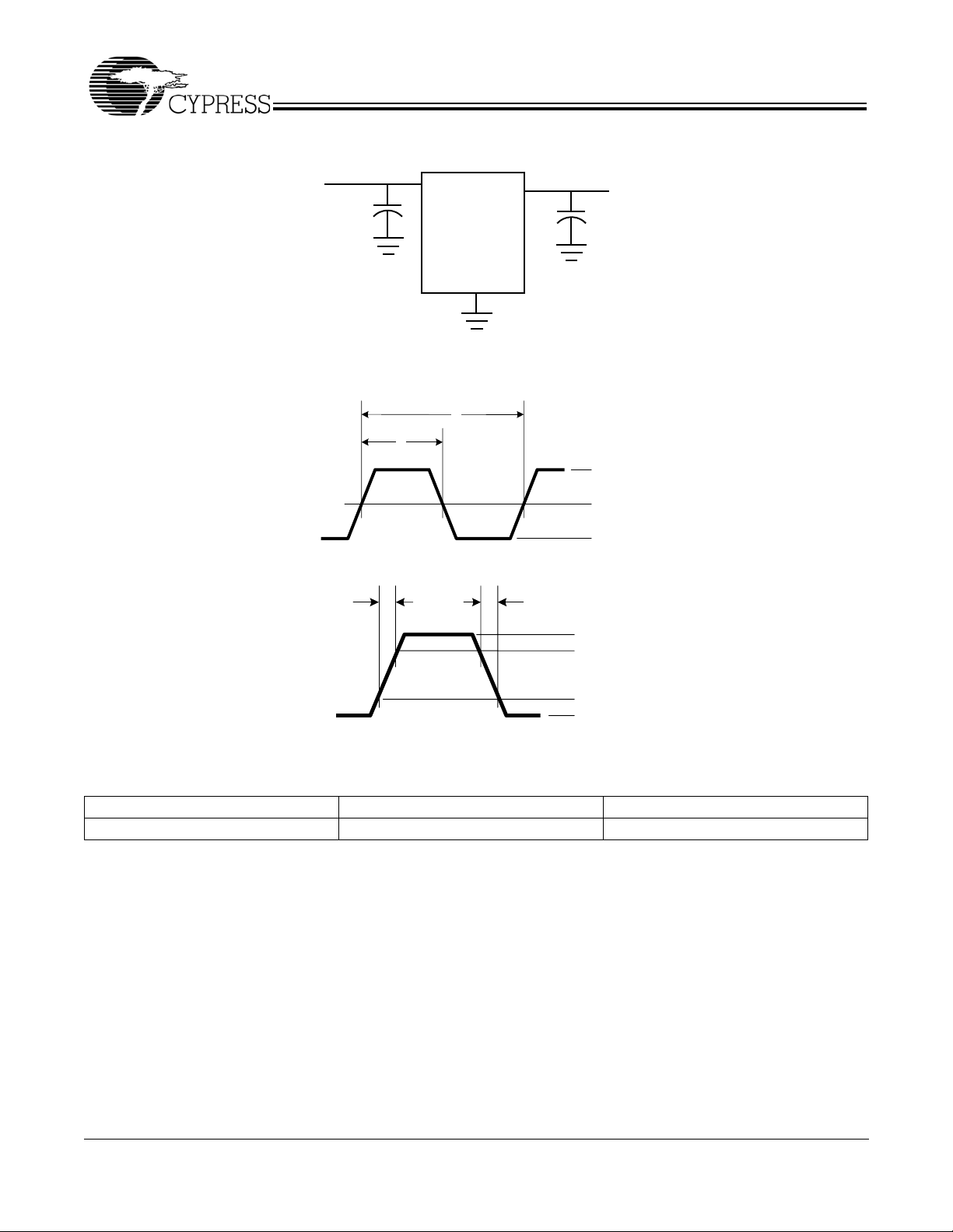
Test and Measurement Set-up
CY2048WAF
VDD
0.1 µF
Voltage and Timing Definitions
Clock
Output
DUT
GND
t
1
t
2
Figure 5. Duty Cycle Definition
t
R
Output
C
LOAD
V
DD
50% of V
0V
t
F
V
DD
80% of V
DD
DD
Clock
Output
20% of V
0V
DD
Figure 6.
Ordering Information
Ordering Code Package Type Operating Range (TJ)
CY2048WAF
Note:
3. The product is offered as tested die-on-wafer form. Contact Cypress Sales for additional programming information and support.
All product or company names mentioned in this document may be the trademarks of their respective holders.
[3]
Wafer Industrial,–40 °C to 125°C
Document #: 38-07738 Rev. *A Page 6 of 7
© Cypress Semiconductor Corporation, 2005. The information contained herein is subject to change wi t hou t notice. Cypress Semiconductor Corporation assumes no responsibility for the use
of any circuitry other than circuitry embodied in a Cypress product. Nor does it convey or imply any license under patent or other rights. Cypress products are not warranted nor intended to be
used for medical, life support, life saving, critical control or safety applications, unless pursuant to an express written agreement with Cypress. Furthermore, Cypress does not auth orize its
products for use as critical components in life-support systems where a malfunction or failure may reasonably be expected to result in significant injury to the user. The inclusion of Cypre ss
products in life-support systems application implies that the manufacturer assumes all risk of such use and in doing so indemnifies Cypress against all charges.
[+] Feedback
Page 7
Document History Page
Document Title: CY2048WAF Flash Programmable Capacitor Tuning Array Die
for Crystal Oscillator(XO)
Document Number: 38-07738
REV. ECN NO. Issue Date
** 319840 See ECN RGL New data sheet
*A 413511 See ECN RGL Minor Change: Pls. post in the web
Orig. of
Change Description of Change
CY2048WAF
Document #: 38-07738 Rev. *A Page 7 of 7
[+] Feedback
 Loading...