

Page 1
PRELIMINARY
CY14B108K, CY14B108M
8 Mbit (1024K x 8/512K x 16) nvSRAM with
Real Time Clock
Features
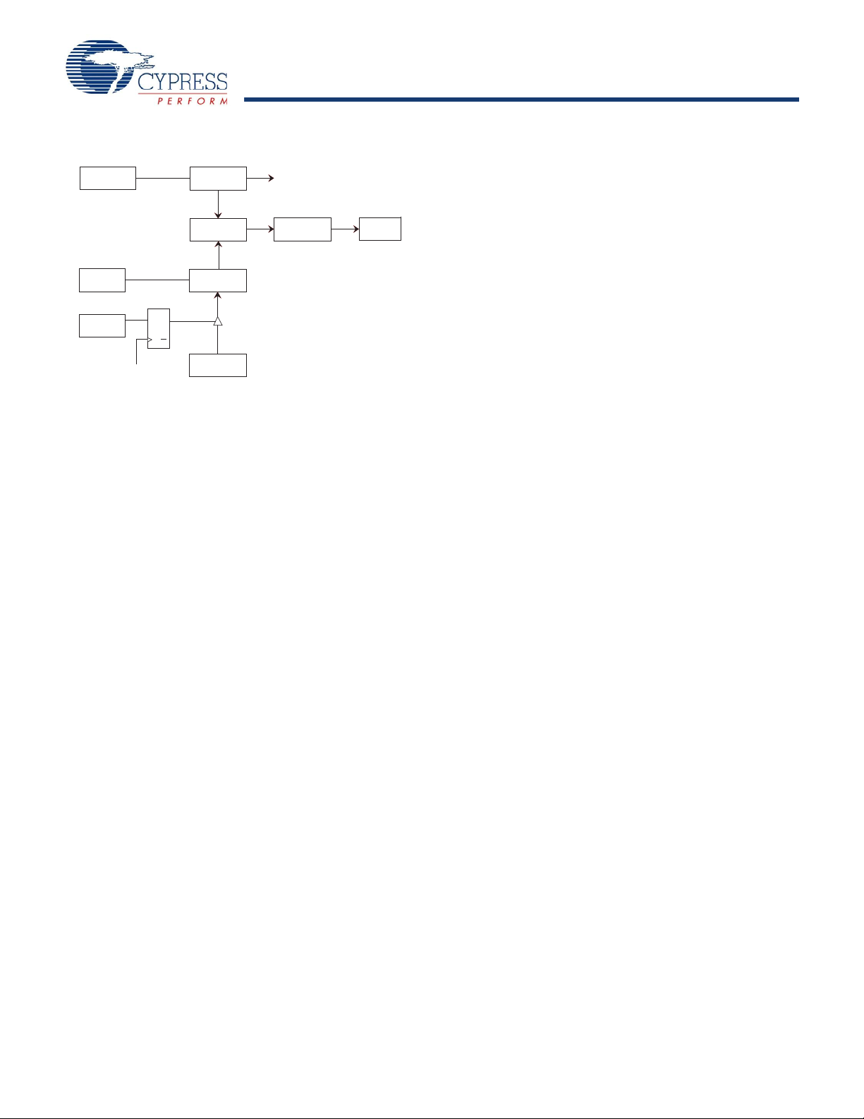
STATIC RAM
ARRAY
2048 X 2048 X 2
R
O
W
D
E
C
O
D
E
R
COLUMN I/O
COLUMN DEC
I
N
P
U
T
B
U
F
F
E
R
S
POWER
CONTROL
STORE/RECALL
CONTROL
Quatrum
Trap
2048 X 2048 X 2
STORE
RECALL
V
CC
V
CAP
HSB
A9A
10
A
11
A12A13A14A15A
16
SOFTWARE
DETECT
A14-A
2
OE
CE
WE
BHE
BLE
A
0
A
1
A
2
A
3
A
4
A
5
A
6
A
7
A
8
A
17
A
18
DQ
0
DQ
1
DQ
2
DQ
3
DQ
4
DQ
5
DQ
6
DQ
7
DQ
8
DQ
9
DQ
10
DQ
11
DQ
12
DQ
13
DQ
14
DQ
15
RTC
MUX A19-A
0
X
out
X
in
INT
V
RTCbat
V
RTCcap
A
19
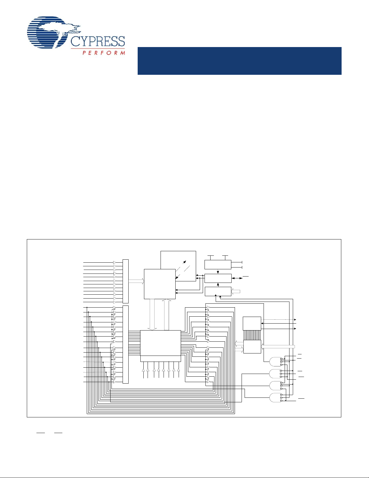
Logic Block Diagram
[1, 2, 3]
Notes
1. Address A
0
- A19 for x8 configuration and Address A0 - A18 for x16 configuration.
2. Data DQ
0
- DQ7 for x8 configuration and Data DQ0 - DQ15 for x16 configuration.
3. BHE
and BLE are applicable for x16 configuration only.
■
20 ns, 25 ns, and 45 ns access times
■
Internally organized as 1024K x 8 (CY14B108K) or 512K x 16
(CY14B108M)
■
Hands off automatic STORE on power down with only a small
capacitor
■
STORE to QuantumTrap® nonvolatile elements is initiated by
software, device pin, or AutoStore
■
RECALL to SRAM initiated by software or power up
■
High reliability
■
Infinite Read, Write, and RECALL cycles
■
200,000 STORE cycles to QuantumTrap
■
20 year data retention
■
Single 3V +20%, –10% operation
■
Data integrity of Cypress nvSRAM combined with full featured
Real Time Clock (RTC)
®
on power down
■
Watchdog timer
■
Clock alarm with programmable interrupts
■
Capacitor or battery backup for RTC
■
Commercial and industrial temperatures
■
44 and 54-pin TSOP II package
■
Pb-free and RoHS compliance
Functional Description
The Cypress CY14B108K/CY14B108M combines a 8-Mbit
nonvolatile static RAM with a full featured RTC in a monolithic
integrated circuit. The embedded nonvolatile elements incorporate QuantumTrap technology producing the world’s most
reliable nonvolatile memory. The SRAM is read and written
infinite number of times, while independent nonvolatile data
resides in the nonvolatile elements.
The RTC function provides an accurate clock with leap year
tracking and a programmable, high accuracy oscillator. The
alarm function is programmable for periodic minutes, hours,
days, or months alarms. There is also a programmable watchdog
timer for process control.
Cypress Semiconductor Corporation • 198 Champion Court • San Jose,CA 95134-1709 • 408-943-2600
Document #: 001-47378 Rev. ** Revised April 01, 2009
[+] Feedback
Page 2
PRELIMINARY
CY14B108K, CY14B108M
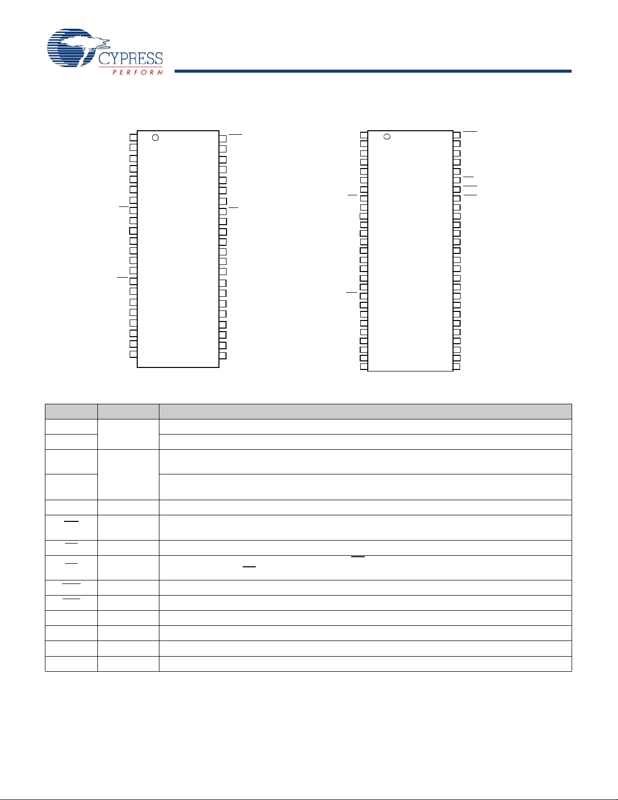
Pinouts
NC
A
8
Xin
Xout
V
SS
DQ
6
DQ5
DQ4
V
CC
A
13
DQ
3
A
12
DQ
2
DQ
1
DQ
0
OE
A
9
CE
NC
A
0
A
1
A
2
A
3
A
4
A
5
A
6
A
11
A
7
A
14
A
15
A
16
A
19
1
2
3
4
5
6
7
8
9
10
11
12
13
14
15
16
17
18
19
20
21
22
23
24
25
26
27
28
29
30
31
32
33
34
35
36
37
38
39
40
41
42
43
44
44 - TSOP II
Top View
(not to scale)
A
10
V
RTCbat
WE
DQ
7
HSB
INT
V
SS
V
CC
V
CAP
V
RTCcap
(x8)
DQ
7
DQ
6
DQ
5
DQ
4
V
CC
DQ
3
DQ
2
DQ
1
DQ
0
NC
A
0
A
1
A
2
A
3
A
4
A
5
A
6
A
7
V
CAP
WE
A
8
A
10
A
11
A
12
A
13
A
14
A
15
1
2
3
4
5
6
7
8
9
10
11
12
13
14
15
16
17
18
19
20
21
22
23
24
25
26
27
28
29
30
31
32
33
34
35
36
37
38
39
40
41
42
43
44
45
46
47
48
54 - TSOP II
Top View
(not to scale)
OE
CE
V
CC
INT
V
SS
NC
A
9
NC
A
18
54
53
52
51
49
50
HSB
BHE
BLE
DQ
15
DQ
14
DQ
13
DQ
12
V
SS
DQ
11
DQ
10
DQ
9
DQ
8
(x16)
V
RTCcap
V
RTCbat
Xin
Xout
[4]
[4]
A
17
A
18
A
16
A
17
Note
4. Address expansion for 16 Mbit. NC pin not connected to die.
Table 1. Pin Definitions
Pin Name I/O Type Description
– A
A
0
19
– A
A
0
18
– DQ7Input/Output Bidirectional Data I/O Lines for x8 Configuration. Used as input or output lines depending on
DQ
0
DQ0 – DQ
15
NC No Connect No Connects. This pin is not connected to the die.
WE
CE
OE
BHE
BLE
X
out
X
in
V
RTCcap
V
RTCbat
Document #: 001-47378 Rev. ** Page 2 of 29
Input Address Inputs Used to Select one of the 1,048,576 bytes of the nvSRAM for x8 Configuration.
Address Inputs Used to Select one of the 524,288 words of the nvSRAM for x16 Configuration.
operation.
Bidirectional Data I/O Lines for x16 Configuration. Used as input or output lines depending on
operation.
Input Write Enable In pu t, Active LOW. When selected LOW, data on the I/O pins is written to the specific
address location.
Input Chip Enable Input, Active LOW. When LOW, selects the chip. When HIGH, deselects the chip.
Input Output Enable, Active LOW. The active LOW OE input enables the data output buffers during read
Input Byte High Enable, Active LOW. Controls DQ15 - DQ8.
Input Byte Low Enable, Active LOW. Controls DQ7 - DQ0.
Output Crystal Connection. Drives crystal on start up.
Input Crystal Connection. For 32.768 KHz crystal.
Power Supply Capacitor Supplied Backup RTC Supply Voltage. Left unconnected if V
Power Supply Battery Supplied Backup RTC Supply Voltage. Left unconnected if V
cycles. Deasserting OE
Figure 1. Pin Diagram: 44-PIn and 54-Pi n TS OP II
HIGH causes the I/O pins to tri-state.
RTCcap
RTCbat
is used.
is used.
[+] Feedback
Page 3
PRELIMINARY
CY14B108K, CY14B108M
Table 1. Pin Definitions (continued)
0.1uF
Vcc
10kOhm
V
CAP
Vcc
WE
V
CAP
V
SS
Pin Name I/O Type Description
INT
V
V
SS
CC
Output Interrupt Output. Programmable to respond to the clock alarm, the watchdog timer, and the power
monitor. Also programmable to either active HIGH (push or pull) or LOW (open drain).
Ground Ground for the Device. Must be connected to ground of the system.
Power Supply Power Supply Inputs to the Device. 3.0V +20%, –10%.
Input/Output Hardware STORE Busy (HSB). When LOW this output indicates that a Hardware STORE is in progress.
HSB
When pulled LOW external to the chip it initiates a nonvolatile STORE operation. A weak internal pull
up resistor keeps this pin HIGH if not connected (connection optional). After each STORE operation
HSB
is driven HIGH for short time with standard output high current.
V
CAP
Power Supply AutoStore Capacitor. Supplies power to the nvSRAM during power loss to store data from SRAM to
nonvolatile elements.
Device Operation
The CY14B108K/CY14B108M nvSRAM is made up of two
functional components paired in the same physical cell. These
are a SRAM memory cell and a nonvolatile QuantumTrap cell.
The SRAM memory cell operates as a standard fast static RAM.
Data in the SRAM is transferred to the nonvolatile cell (the
STORE operation), or from the nonvolatile cell to the SRAM (the
RECALL operation). Using this unique architecture, all cells are
stored and recalled in parallel. During the STORE and RECALL
operations SRAM read and write operations are inhibited. The
CY14B108K/CY14B108M supports infinite reads and writes
similar to a typical SRAM. In addition, it provides infinite RECALL
operations from the nonvolatile cells and up to 200K STORE
operations. See the Truth Table For SRAM Operations on page
24 for a complete description of read and write modes.
SRAM Read
The CY14B108K/CY14B108M performs a read cycle whenever
and OE are LOW, and WE and HSB are HIGH. The address
CE
specified on pins A
1,048,576 data bytes or 524,288 words of 16 bits each are
accessed. Byte enables (BHE
enabled to the output, in the case of 16-bit words. When the read
is initiated by an address transition, the outputs are valid after a
delay of t
the outputs are valid at t
(read cycle 1). If the read is initiated by CE or OE,
AA
cycle 2). The data output repeatedly responds to address
changes within the tAA access time without the need for transitions on any control input pins. This remains valid until another
address change or until CE
is brought LOW.
HSB
0-19
or A
determines which of the
0-18
, BLE) determine which bytes are
ACE
or at t
, whichever is later (read
DOE
or OE is brought HIGH, or WE or
AutoStore Operation
The CY14B108K/CY14B108M stores data to the nvSRAM using
one of three storage operations. These three operations are:
Hardware STORE, activated by the HSB; Software STORE,
activated by an address sequence; AutoStore, on device power
down. The AutoStore operation is a unique feature of
QuantumTrap technology and is enabled by default on the
CY14B108K/CY14B108M.
During normal operation, the device draws current from V
charge a capacitor connected to the V
charge is used by the chip to perform a single STORE operation.
If the voltage on the VCC pin drops below V
automatically disconnects the V
operation is initiated with power provided by the V
pin from VCC. A STORE
CAP
pin. This stored
CAP
SWITCH
capacitor.
CAP
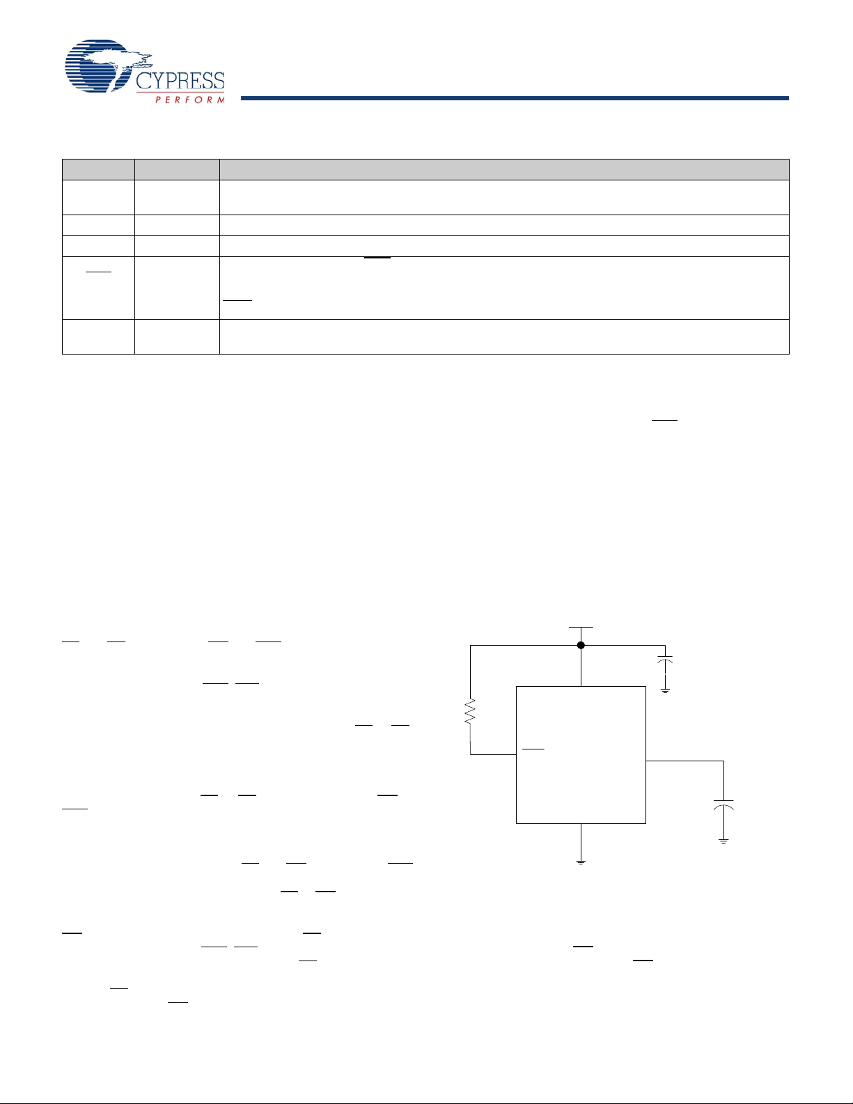
Figure 2. AutoStore Mode
to
CC
, the part
SRAM Write
A write cycle is performed when CE and WE are LOW and HSB
is HIGH. The address inputs must be stable before entering the
write cycle and must remain stable until CE
the end of the cycle. The data on the common I/O pins DO
are written into the memory if it is valid tSD before the end of a
WE
The Byte Enable inputs (BHE
written, in the case of 16-bit words. Keep OE
controlled write or before the end of a CE controlled write.
, BLE) determine which bytes are
or WE goes HIGH at
0-15
HIGH during the
entire write cycle to avoid data bus contention on common I/O
lines. If OE
buffers t
Document #: 001-47378 Rev. ** Page 3 of 29
HZWE
is left LOW, internal circuitry turns off the output
after WE goes LOW.
Figure 2 shows the proper connection of the storage capacitor
(V
) for automatic STORE operation. Refer to DC Electrical
CAP
Characteristics on page 15 for the size of the V
on the V
up should be placed on WE
This pull up is only effective if the WE
pin is driven to V
CAP
by a regulator on the chip. A pull
CC
to hold it inactive during power up.
signal is tri-state during
CAP
power up. Many MPUs tri-state their controls on power up. Verify
this when using the pull up. When the nvSRAM comes out of
. The voltage
[+] Feedback
Page 4

PRELIMINARY
CY14B108K, CY14B108M
power-on-recall, the MPU must be active or the WE
until the MPU comes out of reset.
To reduce unnecessary nonvolatile STOREs, AutoStore, and
Hardware STORE operations are ignored unless at least one
write operation has taken place since the most recent STORE or
RECALL cycle. Software initiated STORE cycles are performed
regardless of whether a write operation has taken place. The
HSB signal is monitored by the system to detect if an AutoStore
cycle is in progress.
held inactive
Hardware STORE (HSB) Operation
The CY14B108K/CY14B108M provides the HSB pin to control
and acknowledge the STORE operations. The HSB
to request a Hardware STORE cycle. When the HSB
LOW, the CY14B108K/CY14B108M conditionally initiates a
STORE operation after t
only if a write to the SRAM has taken place since the last STORE
or RECALL cycle. The HSB pin also acts as an open drain driver
that is internally driven LOW to indicate a busy condition when
the STORE (initiated by any means) is in progress.
SRAM read and write operations, that are in progress when HSB
is driven LOW by any means, are given time t
before the STORE operation is initiated. However, any SRAM
write cycles requested after HSB
returns HIGH. In case the write latch is not set, HSB is not
HSB
driven LOW by the CY14B108K/CY14B108M but any SRAM
read and write cycles are inhibited until HSB
MPU or external source.
During any STORE operation, regardless of how it is initiated,
the CY14B108K/CY14B108M continues to drive the HSB
LOW, releasing it only when the STORE is complete. Upon
completion of the STORE operation, the
CY14B108K/CY14B108M remains disabled until the HSB
returns HIGH. Leave the HSB
. An actual STORE cycle begins
DELAY
goes LOW are inhibited until
is returned HIGH by
unconnected if it is not used.
DELAY
pin is used
pin is driven
to complete
pin
pin
Hardware RECALL (Power Up)
During power up or after any low power condition
(V
CC<VSWITCH
again exceeds the V
V
CC
is automatically initiated and takes t
this time, the HSB
reads and writes to nvSRAM are inhibited.
), an internal RECALL request is latched. When
pin is driven LOW by the HSB driver and all
on powerup, a RECALL cycle
SWITCH
HRECALL
to complete. During
To initiate the Software STORE cycle, the following read
sequence must be performed:
1. Read address 0x4E38 Valid READ
2. Read address 0xB1C7 Valid READ
3. Read address 0x83E0 Valid READ
4. Read address 0x7C1F Valid READ
5. Read address 0x703F Valid READ
6. Read address 0x8FC0 Initiate STORE cycle
The software sequence may be clocked with CE
reads. Both CE
executed. After the sixth address in the sequence is entered, the
STORE cycle starts and the chip is disabled. It is important to use
read cycles and not write cycles in the sequence. The SRAM is
activated again for read and write operations after the t
cycle time.
and OE must be toggled for the sequence to be
or OE controlled
STORE
Software RECALL
Data is transferred from the nonvolatile memory to the SRAM by
a software address sequence. A software RECALL cycle is
initiated with a sequence of read operations in a manner similar
to the Software STORE initiation. To initiate the RECALL cycle,
perform the following sequence of CE
operations:
1. Read address 0x4E38 Valid READ
2. Read address 0xB1C7 Valid READ
3. Read address 0x83E0 Valid READ
4. Read address 0x7C1F Valid READ
5. Read address 0x703F Valid READ
6. Read address 0x4C63 Initiate RECALL cycle
Internally, RECALL is a two step procedure. First, the SRAM data
is cleared; then, the nonvolatile information is transferred into the
SRAM cells. After the t
ready for read and write operations. The RECALL operation
does not alter the data in the nonvolatile elements.
cycle time, the SRAM is again
RECALL
or OE controlled read
Software ST ORE
Data is transferred from the SRAM to the nonvolatile memory by
a software address sequence. The CY14B108K/CY14B108M
Software STORE cycle is initiated by executing sequential CE
controlled read cycles from six specific address locations in
OE
exact order. During the STORE cycle, an erase of the previous
nonvolatile data is first performed, followed by a program of the
nonvolatile elements. After a STORE cycle is initiated, further
input and output are disabled until the cycle is completed.
Because a sequence of reads from specific addresses is used
for STORE initiation, it is important that no other read or write
accesses intervene in the sequence, or the sequence is aborted
and no STORE or RECALL takes place.
Document #: 001-47378 Rev. ** Page 4 of 29
or
[+] Feedback
Page 5

PRELIMINARY
CY14B108K, CY14B108M
Table 2. Mode Selection
Notes
5. While there are 20 address lines on the CY14B108K (19 address lines on the CY14B108M), only the 13 address lines (A
14
- A2) are used to control software modes.
The remaining address lines are don’t care.
6. The six consecutive address locations must be in the order listed. WE
must be HIGH during all six cycles to enable a nonvolatile cycle.
CE WE OE, BHE, BLE
H X X X Not Selected Output High Z Standby
L H L X Read SRAM Output Data Active
L L X X Write SRAM Input Data Active
L H L 0x4E38
L H L 0x4E38
L H L 0x4E38
L H L 0x4E38
0xB1C7
0x83E0
0x7C1F
0x703F
0x8B45
[5]
0
Mode I/O Power
Read SRAM
Read SRAM
Read SRAM
Read SRAM
Read SRAM
AutoStore
Output Data
Output Data
Output Data
Output Data
Output Data
Output Data
Active
[6]
[3]
A15 - A
Disable
0xB1C7
0x83E0
0x7C1F
0x703F
0x4B46
Read SRAM
Read SRAM
Read SRAM
Read SRAM
Read SRAM
AutoStore
Output Data
Output Data
Output Data
Output Data
Output Data
Output Data
Active
[6]
Enable
0xB1C7
0x83E0
0x7C1F
0x703F
0x8FC0
Read SRAM
Read SRAM
Read SRAM
Read SRAM
Read SRAM
Nonvolatile
Output Data
Output Data
Output Data
Output Data
Output Data
Output High Z
Active I
CC2
[6]
STORE
[6]
Active
0xB1C7
0x83E0
0x7C1F
0x703F
0x4C63
Read SRAM
Read SRAM
Read SRAM
Read SRAM
Read SRAM
Nonvolatile
Output Data
Output Data
Output Data
Output Data
Output Data
Output High Z
RECALL
Preventing AutoStore
The AutoStore function is disabled by initiating an AutoStore
disable sequence. A sequence of read operations is performed
in a manner similar to the Software STORE initiation. To initiate
the AutoStore disable sequence, the following sequence of CE
or OE controlled read operations must be performed:
1. Read address 0x4E38 Valid READ
2. Read address 0xB1C7 Valid READ
3. Read address 0x83E0 Valid READ
4. Read address 0x7C1F Valid READ
5. Read address 0x703F Valid READ
6. Read address 0x8B45 AutoStore Disable
manner similar to the software RECALL initiation. To initiate the
AutoStore enable sequence, the following sequence of CE
controlled read operations must be performed:
1. Read address 0x4E38 Valid READ
2. Read address 0xB1C7 Valid READ
3. Read address 0x83E0 Valid READ
4. Read address 0x7C1F Valid READ
5. Read address 0x703F Valid READ
6. Read address 0x4B46 AutoStore Enable
If the AutoStore function is disabled or re-enabled, a manual
STORE operation (hardware or software) issued to save the
AutoStore state through subsequent power down cycles. The
part comes from the factory with AutoStore enabled.
AutoStore is re-enabled by initiating an AutoStore enable
sequence. A sequence of read operations is performed in a
Document #: 001-47378 Rev. ** Page 5 of 29
or OE
[+] Feedback
Page 6

PRELIMINARY
CY14B108K, CY14B108M
Data Protection
Best Practices
The CY14B108K/CY14B108M protects data from corruption
during low voltage conditions by inhibiting all external ly i nitiated
STORE and write operations. The low voltage condition is
detected when V
CY14B108K/CY14B108M is in a write mode (both CE
is less than V
CC
SWITCH
. If the
and WE
are LOW) at power up, after a RECALL or STORE, the write is
inhibited until the SRAM is enabled after t
active). This protects against inadvertent writes during power up
(HSB to output
LZHSB
or brown out conditions.
Noise Considerations
Refer to CY application note AN1064.
nvSRAM products have been used effectively for over 15 years.
While ease-of-use is one of the product’s main system values,
experience gained working with hundreds of applications has
resulted in the following suggestions as best practices:
■
The nonvolatile cells in this nvSRAM product are delivered from
Cypress with 0x00 written in all cells. Incoming inspection
routines at customer or contract manufacturer’s sites
sometimes reprogram these values. Final NV patterns are
typically repeating patterns of AA, 55, 00, FF, A5, or 5A. End
product’s firmware should not assume an NV array is in a set
programmed state. Routines that check memory content
values to determine first time system configuration, cold or
warm boot status, and so on should always program a unique
NV pattern (that is, complex 4-byte pattern of 46 E6 49 53 hex
or more random bytes) as part of the final system manufacturing test to ensure these system routines work consistently.
■
Power up boot firmware routines should rewrite the nvSRAM
into the desired state (for example, autostore enabled). While
the nvSRAM is shipped in a preset state, best practice is to
again rewrite the nvSRAM into the desired state as a safeguard
against events that might flip the bit inadvertently such as
program bugs and incoming inspection routines.
■
The V
CAP
value specified in this data sheet includes a minimum
and a maximum value size. Best practice is to meet this
requirement and not exceed the maximum V
the nvSRAM internal algorithm calculates V
discharge time based on this maximum V
that want to use a larger V
CAP
value to make sure there is extra
store charge and store time should discuss their V
selection with Cypress to understand any impact on the V
voltage level at the end of a t
RECALL
period.
CAP
value because
CAP
charge and
value. Customers
CAP
CAP
size
CAP
Document #: 001-47378 Rev. ** Page 6 of 29
[+] Feedback
Page 7
PRELIMINARY
CY14B108K, CY14B108M
Real Time Clock Operation
nvTime Operation
The CY14B108K/CY14B108M offers internal registers that
contain clock, alarm, watchdog, interrupt, and control functions.
RTC registers use the last 16 address locations of the SRAM.
Internal double buffering of the clock and timer information
registers prevents accessing transitional internal clock data
during a read or write operation. Double buffering also
circumvents disrupting normal timing counts or the clock
accuracy of the internal clock when accessing clock data. Clock
and alarm registers store data in BCD format.
RTC functionality is described with respect to CY14B108K in the
following sections. The same description applies to
CY14B108M, except for the RTC register addresses. The RTC
register addresses for CY14B108K range from 0xFFFF0 to
0xFFFFF, while those for CY14B108M range from 0x7FFF0 to
0x7FFFF. Refer to Table 4 on page 11 and Ta bl e 5 on page 12
for a detailed Register Map description.
Clock Operations
The clock registers maintain time up to 9,999 years in one
second increments. The time can be set to any calendar time and
the clock automatically keeps track of days of the week and
month, leap years, and century transitions. There are eight
registers dedicated to the clock functions, which are used to set
time with a write cycle and to read time during a read cycle.
These registers contain the time of day in BCD format. Bits
defined as ‘0’ are currently not used and are reserved for future
use by Cypress.
Reading the Clock
The double buffered RTC register structure reduces the chance
of reading incorrect data from the clock. The user must stop
internal updates to the CY14B108K time keeping registers
before reading clock data, to prevent reading of data in transition.
Stopping the register updates does not affect clock accuracy.
The updating process is stopped by writing a ‘1’ to the read bit
‘R’ (in the flags register at 0xFFFF0), and does not restart until a
‘0’ is written to the read bit. The RTC registers are then read while
the internal clock continues to run. After a ‘0’ is written to the read
bit (‘R’), all RTC registers are simultaneously updated within
20 ms
Setting the Clock
Setting the write bit ‘W’ (in the flags register at 0xFFFF0) to a ‘1’
stops updates to the time keeping registers and enables the time
to be set. The correct day, date, and time is then written into the
registers and must be in 24 hou r BCD format. T he time writ ten is
referred to as the “Base Time”. This value is stored in nonvolatile
registers and used in the calculation of the current time.
Resetting the write bit to ‘0’ transfers the values of timekeeping
registers to the actual clock counters, after which the clock
resumes normal operation.
If the time written to the timekeeping registers is not in the correct
BCD format, each invalid nibble of the RTC registers continue
counting to 0xF before rolling over to 0x0 after which RTC
resumes normal operation.
Note The values entered in the timekeeping, alarm, calibration,
and interrupt registers need a STORE operation to be saved in
nonvolatile memory. Therefore, while working in AutoStore
disabled mode, the user must perform a STORE operation after
writing into the RTC registers for the RTC to work correctly.
Backup Power
The RTC in the CY14B108K is intended for permanently
powered operation. The V
depending on whether a capacitor or battery is chosen for the
application. When the primary power, VCC, fails and drops below
V
The clock oscillator uses very little current, which maximizes the
backup time available from the backup source. Regardless of the
clock operation with the primary source removed, the data stored
in the nvSRAM is secure, having been stored in the nonvolatile
elements when power was lost.
During backup operation, the CY14B108K consumes a
maximum of 300 nanoamps at room temperature. User must
choose capacitor or battery values according to the application.
Backup time values based on maximum current specifications
are shown in the following table. Nominal backup times are
approximately two times longer.
Table 3. RTC Backup Time
Using a capacitor has the obvious advantage of recharging the
backup source each time the system is powered up. If a battery
is used, a 3V lithium is recommended and the CY14B108K
sources current only from the battery when the primary power is
removed. However, the battery is not recharged at any time by
the CY14B108K. The battery capacity must be chosen for total
anticipated cumulative down time required over the life of the
system.
the device switches to the backup power supply.
SWITCH
Capacitor Value Backup Time
0.1F 72 hours
0.47F 14 days
1.0F 30 days
RTCcap
or V
pin is connected
RTCbat
Stopping and Starting the Oscillator
The OSCEN bit in the calibration register at 0xFFFF8 controls
the enable and disable of the oscillator. This bit is nonvolatile and
is shipped to customers in the “enabled” (set to 0) state. To
preserve the battery life when the system is in storage, OSCEN
must be set to ‘1’. This turns off the oscillator circuit, extending
the battery life. If the OSCEN bit goes from disabled to enabled,
it takes approximately one second (two seconds maximum) for
the oscillator to start.
While system power is off, If the voltage on the backup supply
(V
the oscillator may fail.The CY14B108K has the ability to detect
oscillator failure when system power is restored. This is recorded
in the OSCF (Oscillator Failed bit) of the flags register at the
address 0xFFFF0. When the device is powered on (V
above V
If the OSCEN bit is enabled and the oscillator is not active within
the first 5 ms, the OSCF bit is set to “1”. The system must check
for this condition and then write ‘0’ to clear th e flag. N ote that in
addition to setting the OSCF flag bit, the time registers are reset
to the “Base Time” (see Setting the Clock on page 7), which is
the value last written to the timekeeping registers. The control or
RTCcap
or V
SWITCH
) falls below their respective minimum level,
RTCbat
) the OSCEN bit is checked for “enabled” status.
CC
goes
Document #: 001-47378 Rev. ** Page 7 of 29
[+] Feedback
Page 8

PRELIMINARY
CY14B108K, CY14B108M
calibration registers and the OS CEN bit are not affected by the
‘oscillator failed’ condition.
The value of OSCF must be reset to ‘0’ when the time reg isters
are written for the first time. This initializes the state of this bit
which may have become set when the system was first powered
on.
To reset OSCF, set the write bit “W” (in the Flags register at
0xFFFF0) to a “1” to enable writes to the Flag register. Write a
“0” to the OSCF bit and then reset the write bit to “0” to disable
writes.
Calibrating the Clock
The RTC is driven by a quartz controlled crystal with a nominal
frequency of 32.768 kHz. Clock accuracy depends on the quality
of the crystal and calibration. The crystals available in market
typically have an error of +
CY14B108K employs a calibration circuit that improves the
accuracy to +1/–2 ppm at 25°C. This implies an error of +2.5
seconds to -5 seconds per month.
The
calibration circuit adds or subtracts counts from the oscillator
divider circuit to achieve this accuracy. The number of pulses that
are suppressed (subtracted, negative calibration) or split (added,
positive calibration) depends upon the value loaded into the five
calibration bits found in Calibration register at 0xFFFF8. The
calibration bits occupy the five lower order bits in the Calibration
register. These bits are set to represent any value between ‘0’
and 31 in binary form. Bit D5 is a sign bit, where a ‘1’ indicates
positive calibration and a ‘0’ indicates negative calibration.
Adding counts speeds the clock up and subtracting counts slows
the clock down. If a binary ‘1’ is loaded into the register, it corresponds to an adjustment of 4.068 or –2.034 ppm offset in oscillator error, depending on the sign.
Calibration occurs within a 64-minute cycle. The first 62 minutes
in the cycle may, once every minute, have one second shortened
by 128 or lengthened by 256 oscillator cycles. If a binary ‘1’ is
loaded into the register, only the first two minutes of the
64-minute cycle are modified. If a binary 6 is loaded, the first 12
are affected, and so on. Therefore, each calibration step has the
effect of adding 512 or subtracting 256 oscillator cycles for every
125,829,120 actual oscillator cycles, that is, 4.068 or –2.034 ppm
of adjustment per calibration step in the Calibration register.
To determine the required calibration, the CAL bit in the Flags
register (0xFFFF0) must be set to ‘1’. This causes the INT pin to
toggle at a nominal frequency of 512 Hz. Any deviation
measured from the 512 Hz indicates the degree and direction of
the required correction. For example, a reading of 512.01024 Hz
indicates a +20 ppm error. Hence, a decimal value of –10
(001010b) must be loaded into the Calibration register to offset
this error.
Note Setting or changing the Calibration register does not affect
the test output frequency.
To set or clear CAL, set the write bit “W” (in the flags register at
0xFFFF0) to “1” to enable writes to the Flag register. Write a
value to CAL, and then reset the write bit to “0” to disable writes.
20 ppm to +35 ppm. However,
Alarm
The alarm function compares user programmed values of alarm
time and date (stored in the registers 0xFFFF1-5) with the corresponding time of day and date values. When a match occurs, the
alarm internal flag (AF) is set and an interrupt is generated on
INT pin if Alarm Interrupt Enable (AIE) bit is set.
There are four alarm match fields - date, hours, minutes, and
seconds. Each of these fields has a match bit that is used to
determine if the field is used in the alarm match logic. Setting the
match bit to ‘0’ indicates that the corresponding field is used in
the match process. Depending on the match bits, the alarm
occurs as specifically as once a month or as frequently as once
every minute. Selecting none of the match bits (all 1s) indicates
that no match is required and therefore, alarm is disabled.
Selecting all match bits (all 0s) causes an exact time an d date
match.
There are two ways to detect an alarm event: by reading the AF
flag or monitoring the INT pin. The AF flag in the flags register at
0xFFFF0 indicates that a date or time match has occurred. The
AF bit is set to “1” when a match occurs. Reading the flags
register clears the alarm flag bit (and all others). A hardware
interrupt pin may also be used to detect an alarm event.
T o set, clear or enable an alarm, set the ‘W’ bit (in Flags Register
- 0xFFFF0) to ‘1’ to enable writes to Alarm Registers. After
writing the alarm value, clear the ‘W’ bit back to “0” for the
changes to take effect.
Note CY14B108K requires the alarm match bit for seconds
(0xFFFF2 - D7) to be set to ‘0’ for proper operation of Alarm Flag
and Interrupt.
Watchdog Timer
The Watchdog Timer is a free running down counter that uses
the 32 Hz clock (31.25 ms) derived from the crystal oscillator.
The oscillator must be running for the watchdog to function. It
begins counting down from the value loaded in the Watchdog
Timer register.
The timer consists of a loadable register and a free running
counter. On power up, the watchdog time out value in register
0xFFFF7 is loaded into the Counter Load register. Counting
begins on power up and restarts from the loadable value any time
the Watchdog Strobe (WDS) bit is set to ‘1’. The counter is
compared to the terminal value of ‘0’. If the counter reaches this
value, it causes an internal flag and an optional interrupt output.
You can prevent the time out interrupt by setting WDS bit to ‘1’
prior to the counter reaching ‘0’. This causes the counter to
reload with the watchdog time out value and to be restarted. As
long as the user sets the WDS bit prior to the counter reaching
the terminal value, the interrupt and WDT flag never occur.
New time out values are written by setting the watchdog write bit
to ‘0’. When the WDW is ‘0’, new writes to the watchdog time out
value bits D5-D0 are enabled to modify the time out value. When
WDW is ‘1’, writes to bits D5-D0 are ignored. The WDW function
enables a user to set the WDS bit without concern that the
watchdog timer value is modified. A logical diagram of the
watchdog timer is shown in Figure 3. Note that setting the
watchdog time out value to ‘0’ disables the watchdog function.
The output of the watchdog timer is the flag bit WDF that is set if
the watchdog is allowed to time out. If the Watchdog Interrupt
Enable (WIE) bit in the Interrupt register is set, a hardware
interrupt on INT pin is also generated on watchdog timeout. The
flag and the hardware interrupt are bo th cleared when user reads
the Flags registers.
Document #: 001-47378 Rev. ** Page 8 of 29
[+] Feedback
Page 9
PRELIMINARY
CY14B108K, CY14B108M
Figure 3. Watchdog Timer Block Diagram
1 Hz
Oscillator
Clock
Divider
Counter
Zero
Compare
WDF
WDS
Load
Register
WDW
D
Q
Q
Watchdog
Register
write to
Watchdog
Register
32 Hz
32,768 KHz
.
Power Monitor
The CY14B108K provides a power management sche me with
power fail interrupt capability. It also controls the internal switch
to backup power for the clock and protects the memory from low
V
access. The power monitor is based on an internal band gap
CC
reference circuit that compares the V
threshold.
voltage to V
CC
As described in the section AutoStore Operation on page 3,
when V
STORE operation is initiated from SRAM to the nonvolatile
is reached as VCC decays from power loss, a data
SWITCH
elements, securing the last SRAM data state. Power is also
switched from V
operate the RTC oscillator.
to the backup supply (battery or capacitor) to
CC
When operating from the backup source, read and write operations to nvSRAM are inhibited and the clock functions are not
available to the user. The clock continues to operate in the
background. The updated clock data is available to the user
t
HRECALL
AutoStore/Power Up RECALL on page 21)
delay after VCC is restored to the device (see
Interrupts
The CY14B108K has Flags register, Interrupt register, and
Interrupt logic that can signal interrupt to the microcontroller.
There are three potential sources for interrupt: watchdog timer,
power monitor, and alarm timer . Each of these can be individually
enabled to drive the INT pin by appropriate setting in the Interrupt
register (0xFFFF6). In addition, each has an associated flag bit
in the Flags register (0xFFFF0) that the host processor uses to
determine the cause of the interrupt. The INT pin driver has two
bits that specify its behavior when an interrupt occurs.
An Interrupt is raised only if both a flag is raised by one of the
three sources and the respective interrupt enable bit in Interrupts
register is enabled (set to ‘1’). After an interrupt source is active,
two programmable bits, H/L and P/L, determine the behavior of
the output pin driver on INT pin. These two bits are located in the
Interrupt register and can be used to drive level or pulse mode
SWITCH
output from the INT pin. In pulse mode, the pulse width is
internally fixed at approximately 200 ms. This mode is intended
to reset a host microcontroller. In the level mode, the pin goes to
its active polarity until the Flags register is read by the user. This
mode is used as an interrupt to a host microcontroller. The
control bits are summarized in the following section.
Interrupts are only generated while working on normal power and
are not triggered when system is running in backup power mode.
Note CY14B108K generates valid interrupts only after the
Powerup Recall sequence is completed. All events on INT pin
must be ignored for t
HRECALL
duration after powerup.
Interrupt Register
Watchdog Interrupt Enable (WIE). When set to ‘1’, the
watchdog timer drives the INT pin and an internal flag when a
watchdog time out occurs. When WIE is set to ‘0’, the watchdog
timer only affects the WDF flag in Flags register.
Alarm Interrupt Enable (AIE). When set to ‘1’, the alarm match
drives the INT pin and an internal flag. When AIE is set to ‘0’, the
alarm match only affects the AF Flags register.
Power Fail Interrupt Enable (PFE). When set to ‘1’, the power
fail monitor drives the pin and an internal flag. When PFE is set
to ‘0’, the power fail monitor only affects the PF flag in Flags
register.
High/Low (H/L). When set to a ‘1’, the INT pin is active HIGH
and the driver mode is push pull. The INT p in drives high only
when V
is active LOW and the drive mode is open drain. The INT pin
is greater than V
CC
. When set to a ‘0’, the INT pin
SWITCH
must be pulled up to Vcc by a 10k resistor while using the
interrupt in active LOW mode.
Pulse/Level (P/L). When set to a ‘1’ and an interrupt occurs, the
INT pin is driven for approximately 200 ms. When P/L is set to a
‘0’, the INT pin is driven high or low (determined by H/L) until the
Flags or Control register is read.
When an enabled interrupt source activates the INT pin, an
external host reads the Flags registers to determine the cause.
Remember that all flags are cleared when the register is read. If
the INT pin is programmed for Level mo de, then the condition
clears and the INT pin returns to its inactive state. If the pin is
programmed for Pulse mode, then reading the flag also clears
the flag and the pin. The pulse does not complete i ts specified
duration if the Flags register is read. If the INT pin is used as a
host reset, the Flags register is not read during a reset
Flags Register
The Flag register has three flag bits: WDF , AF, and PF , which can
be used to generate an interrupt. They are set by the watchdog
timeout, alarm match, or power fail monitor respectively. The
processor can either poll this register or enable interrupts when
a flag is set. These flags are automatically reset when the
register is read. The flags register is automatically l oaded with
the value 0x00 on power up (except for the OSCF bit. See
Stopping and Starting the Oscillator on page 7)
Document #: 001-47378 Rev. ** Page 9 of 29
[+] Feedback
Page 10

PRELIMINARY
CY14B108K, CY14B108M
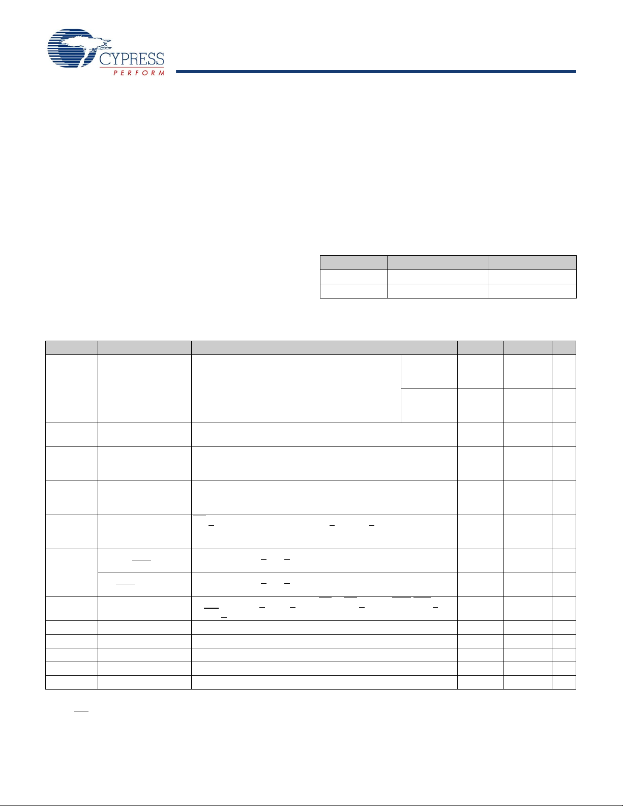
Figure 4. RTC Recommended Component Configuration
Recommended Values
Y
1
= 32.768 KHz (6 pF)
C
1
= 21 pF
C2 = 21 pF
Note: The recommended values for C1 and C2 include
board trace capacitance.
X
out
X
in
Y1
C2
C1
Watchdog
Timer
Power
Monitor
Clock
Alarm
VINT
WDF
WIE
PF
PFE
AF
AIE
P/L
Pin
Driver
H/L
INT
V
CC
V
SS
WDF - Watchdog Timer Flag
WIE - Watchdog Interrupt
PF - Power Fail Flag
PFE - Power Fail Enable
AF - Alarm Flag
AIE - Alarm Interrupt Enable
P/L - Pulse Level
H/L - High/Low
Enable
Figure 5. Interrupt Block Diagram
Document #: 001-47378 Rev. ** Page 10 of 29
[+] Feedback
Page 11
PRELIMINARY
CY14B108K, CY14B108M
Table 4. RTC Register Map
Notes
7. Upper Byte D
15-D8
(CY14B108M) of RTC registers are reserved for future use
8. ( ) designates values shipped from the factory.
9. This is a binary value, not a BCD value.
Register BCD Format Data
CY14B108K CY14B108M D7 D6 D5 D4 D3 D2 D1 D0
[7]
[8]
Function/Range
0xFFFFF 0x7FFFF 10s Years Years Years: 00 –99
0xFFFFE 0x7FFFE 0 0 0 10s
Months Months: 01–12
Months
0xFFFFD 0x7FFFD 0 0 10s Day of Month Day Of Month Day of Month: 01–31
0xFFFFC 0x7FFFC 0 0 0 0 0 Day of week Day of week: 01–07
0xFFFFB 0x7FFF B 0 0 10s Hours Hours Hours: 00–23
0xFFFFA 0x7FFFA 0 10s Minutes Minutes Minutes: 00–59
0xFFFF9 0x7FFF9 0 10s Seconds Seconds Seconds: 00–59
0xFFFF8 0x7FFF8 OSCEN
(0)
0xFFFF7 0x7FFF7 WDS
0Cal Sign
Calibration (00000) Calibration Values
(0)
WDW (0) WDT (000000) Watchdog
(0)
0xFFFF6 0x7FFF6 WIE (0) AIE (0) PFE (0) 0 H/L
P/L (0) 0 0 Interrupts
(1)
0xFFFF5 0x7FFF5 M (1) 0 10s Alarm Date Alarm Day Alarm, Day of Mon th:
01–31
0xFFFF4 0x7FFF4 M (1) 0 10s Alarm Hours Alarm Hours Alarm, Hours: 00–23
0xFFFF3 0x7FFF3 M (1) 10 Alarm Minutes Alarm Minutes Alarm, Minutes:
00–59
0xFFFF2 0x7FFF2 M (1) 10 Alarm Seconds Alarm, Seconds Alarm, Seconds:
00–59
0xFFFF1 0x7FFF1 10s Centuries Centuries Centuries: 00–99
0xFFFF0 0x7FFF0 WDF AF PF OSCF 0 CAL (0) W (0) R (0) Flags
[9]
[9]
[9]
[9]
Document #: 001-47378 Rev. ** Page 11 of 29
[+] Feedback
Page 12

PRELIMINARY
CY14B108K, CY14B108M
Table 5. Register Map Detail
Register
CY14B108K CY14B108M
0xFFFFF 0x7FFFF
0xFFFFE 0x7FFFE
0xFFFFD 0x7FFFD
0xFFFFC 0x7FFFC
0xFFFFB 0x7FFFB
0xFFFFA 0x7FFFA
0xFFFF9 0x7FFF9
Description
Time Keeping - Years
D7 D6 D5 D4 D3 D2 D1 D0
10s Years Years
Contains the lower two BCD digits of the year. Lower nibble (four bits) contains the value for years;
upper nibble (four bits) contains the value for 10s of years. Each nibble operates from 0 to 9. The
range for the register is 0–99.
Time Keeping - Months
D7 D6 D5 D4 D3 D2 D1 D0
0 0 0 10s Month Months
Contains the BCD digits of the month. Lower nibble (four bits) contains the lower digit and operates
from 0 to 9; upper nibble (one bit) contains the upper digit and operates from 0 to 1. The range
for the register is 1–12.
Time Keeping - Date
D7 D6 D5 D4 D3 D2 D1 D0
0 0 10s Day of Month Day of Month
Contains the BCD digits for the date of the month. Lower nibble (four bits) contains the lower digit
and operates from 0 to 9; upper nibble (two bits) contains the 10s digit and operates from 0 to 3.
The range for the register is 1–31. Leap years are automatically adjuste d for.
Time Keeping - Day
D7 D6 D5 D4 D3 D2 D1 D0
0 0 0 0 0 Day of Week
Lower nibble (three bits) contains a value that correlates to day of the week. Day of the week is a
ring counter that counts from 1 to 7 then returns to 1. The user must assign meaning to the day
value, because the day is not integrated with the date.
Time Keeping - Hours
D7 D6 D5 D4 D3 D2 D1 D0
0 0 10s Hours Hours
Contains the BCD value of hours in 24 hour format. Lower nibble (four bits) contains the lower
digit and operates from 0 to 9; upper nibble (two bits) contains the upper digit and operates from
0 to 2. The range for the register is 0–23.
Time Keeping - Minutes
D7 D6 D5 D4 D3 D2 D1 D0
0 10s Minutes Minutes
Contains the BCD value of minutes. Lower nibble (four bits) contains the lower digit and operates
from 0 to 9; upper nibble (three bits) contains the upper minutes digit and operates from 0 to 5.
The range for the register is 0–59.
Time Keeping - Seconds
D7 D6 D5 D4 D3 D2 D1 D0
0 10s Seconds Seconds
Contains the BCD value of seconds. Lower nibble (four bits) contains the lower digit and operates
from 0 to 9; upper nibble (three bits) contains the upper digit and operates from 0 to 5. The range
for the register is 0 to 59.
Document #: 001-47378 Rev. ** Page 12 of 29
[+] Feedback
Page 13

PRELIMINARY
CY14B108K, CY14B108M
Table 5. Register Map Detail (continued)
Register
CY14B108K CY14B108M
0xFFFF8 0x7FFF8
OSCEN Oscillator Enable. When set to 1, the oscillator is stopped. When set to 0, the oscillator runs.
Calibration
Sign
Calibration These five bits control the calibration of the clock.
0xFFFF7 0x7FFF7
WDS Watchdog Strobe. Setting this bit to 1 reloads and restarts the watchdog timer. Setting the bit to
WDW Watchdog Write Enable. Setting this bit to 1 disables any WRITE to the watchdog timeout value
WDT Watchdog timeout selection. The watchdog timer interval is selected by the 6-bit value in this
0xFFFF6 0x7FFF6
WIE Watchdog Interrupt Enable. When set to 1 and a watchdog timeout occurs, the watchdog timer
AIE Alarm Interrupt Enable. When set to 1, the alarm match drives the INT pin and the AF flag. When
PFE Power Fail Enable. When set to 1, the power fail monitor drives the INT pin and the PF flag. When
0 Reserved for future use
H/L High/Low. When set to 1, the INT pin is driven active HIGH. When set to 0, the INT pin is open
P/L Pulse/Level. When set to 1, the INT pin is driven active (determined by H/L) by an interrupt source
0xFFFF5 0x7FFF5
M Match. When this bit is set to 0, the date value is used in the alarm match. Setting this bit to 1
D7 D6 D5 D4 D3 D2 D1 D0
OSCEN 0 Calibration
Disabling the oscillator saves battery or capacitor power during storage.
Determines if the calibration adjustment is applied as an addition (1) to or as a subtraction (0) from
the time-base.
D7 D6 D5 D4 D3 D2 D1 D0
WDS WDW WDT
0 has no effect. The bit is cleared automatically after the watchdog timer is reset. The WDS bit is
write only. Reading it always returns a 0.
(D5–D0). This allows the user to set the watchdog strobe bit without disturbing the timeout value.
Setting this bit to 0 allows bits D5–D0 to be written to the watchdog register when the next write
cycle is complete. This function is explained in more detail in Watchdog Timer on page 8.
register. It represents a multiplier of the 32 Hz count (31.25 ms). The range of timeout value is
31.25 ms (a setting of 1) to 2 seconds (setting of 3 Fh). Setting the watchdog timer register to 0
disables the timer. These bits can be written only if the WDW bit was set to 0 on a previous cycle.
D7 D6 D5 D4 D3 D2 D1 D0
WIE AIE PFE 0 H/L P/L 0 0
drives the INT pin and the WDF flag. When set to 0, the watchdog timeout affects only the WDF
flag.
set to 0, the alarm match only affects the AF flag.
set to 0, the power fail monitor affects only the PF flag.
drain, active LOW.
for approximately 200 ms. When set to 0, the INT pin is driven to an active level (as set by H/L)
until the flags register is read.
D7 D6 D5 D4 D3 D2 D1 D0
M 0 10s Alarm Date Alarm Date
Contains the alarm value for the date of the month and the mask bit to select or deselect the date
value.
causes the match circuit to ignore the date value.
Description
Calibration/Control
Calibration
Sign
WatchDog Timer
Interrupt Stat us /Con tr ol
Alarm - Day
Document #: 001-47378 Rev. ** Page 13 of 29
[+] Feedback
Page 14

PRELIMINARY
CY14B108K, CY14B108M
Table 5. Register Map Detail (continued)
Register
CY14B108K CY14B108M
0xFFFF4 0x7FFF4
M Match. When this bit is set to 0, the hours value is used in the alarm match. Setting this bit to 1
0xFFFF3 0x7FFF3
M Match. When this bit is set to 0, the minutes value is used in the alarm match. Setting this bit to 1
0xFFFF2 0x7FFF2
M Match. When this bit is set to 0, the seconds value is used in the alarm match. Setting this bit to
0xFFFF1 0x7FFF1
0xFFFF0 0x7FFF0
WDF Watchdog Timer Flag. This read only bit is set to 1 when the watchdog timer is allowed to reach
AF Alarm Flag. Thi s read only bit is set to 1 when the time and date match the values stored in the
PF Power Fail Flag. This re ad only bit is set to 1 when power falls below the power fail threshold
OSCF Oscillator Fail Flag. Set to 1 on power up if the oscillator is enabled and not running in the first 5
CAL Calibration Mode. When set to 1, a 512 Hz square wave is output on the INT pin. When set to 0,
W Write Enable: Setting the W bit to 1 freezes updates of the RTC registers. The user can then write
R Read Enable: Setting R bit to 1, stops clock updates to user RTC registers so that clock updates
D7 D6 D5 D4 D3 D2 D1 D0
M 10s Alarm Hours Alarm Hours
Contains the alarm value for the hours and the mask bit to select or deselect the hours value.
causes the match circuit to ignore the hours value.
D7 D6 D5 D4 D3 D2 D1 D0
M 10s Alarm Minutes Alarm Minutes
Contains the alarm value for the minutes and the mask bit to select or deselect the minutes value.
causes the match circuit to ignore the minutes value.
D7 D6 D5 D4 D3 D2 D1 D0
M 10s Alarm Seconds Alarm Seconds
Contains the alarm value for the seconds and the mask bit to select or deselect the seconds’ value.
1 causes the match circuit to ignore the seconds value.
D7 D6 D5 D4 D3 D2 D1 D0
Contains the BCD value of centuries. Lower nibble contains the lower digit and operates from 0
to 9; upper nibble contains the upper digit and operates from 0 to 9. The range for the register is
0-99 centuries.
D7 D6 D5 D4 D3 D2 D1 D0
WDF AF PF OSCF 0 CAL W R
0 without being reset by the user. It is cleared to 0 when the Flags register is read or on power up
alarm registers with the match bits = 0. It is cleared when the Flags register is read or on power up.
V
SWITCH
ms of operation. This indicates that RTC backup power failed and clock value is no longer valid.
This bit survives power cycle and is never cleared internally by the chip. The user must check for
this condition and write '0' to clear this flag.
the INT pin resumes normal operation. This bit defaults to 0 (disabled) on power up.
to RTC registers, Alarm registers, Calibration register, Interrupt register and Flags register . Setting
the W bit to 0 causes the contents of the RTC registers to be transferred to the time keeping
counters if the time is changed (a new base time is loaded). This bit defaults to 0 on power up.
are not seen during the reading process. Set R bit to 0 to resume clock updates to the holding
register. Setting this bit does not require W bit to be set to 1. This bit defaults to 0 on power up.
Description
Alarm - Hours
Alarm - Minutes
Alarm - Seconds
Time Keeping - Centuries
10s Centuries Centuries
Flags
. It is cleared to 0 when the Flags register is read or on power up.
Document #: 001-47378 Rev. ** Page 14 of 29
[+] Feedback
Page 15
PRELIMINARY
CY14B108K, CY14B108M
Maximum Ratings
Notes
10.Typical conditions for the active current shown in DC Electrical Characteristics are average values at 25°C (room temperature), and V
CC
= 3V. Not 100% tested.
11.The HSB
pin has I
OUT
= -2 uA for VOH of 2.4V when both active HIGH and LOW drivers are disabled. When they are enabled standard VOH and VOL are valid. This
parameter is characterized but not tested.
12.V
CAP
(Storage capacitor) nominal value is 150 uF.
Exceeding maximum ratings may impair the useful life of the
device. These user guidelines are not tested.
Storage Temperature ................................. –65°C to +150°C
Maximum Accumulated Storage Time
At 150°C Ambient Temperature................................... 1000h
At 85°C Ambient Temperature..................... ........... 20 Years
Ambient Temperature with
Power Applied ............................................–55°C to +150°C
Supply Voltage on V
Voltage Applied to Outputs
in High-Z State.......................................–0.5V to V
Input Voltage..................... ......................–0.5V to Vcc + 0.5V
Relative to GND..........–0.5V to 4.1V
CC
CC
+ 0.5V
Transient Voltage (<20 ns) on
Any Pin to Ground Potential..................–2.0V to V
CC
+ 2.0V
Package Power Dissipation
Capability (T
= 25°C) ...................................................1.0W
A
Surface Mount Pb Soldering
Temperature (3 Seconds).......................................... +260°C
DC Output Current (1 output at a time, 1s duration).....15 mA
Static Discharge Voltage.......................................... > 2001V
(per MIL-STD-883, Method 3015)
Latch Up Current................................................... > 200 mA
Operating Range
Range Ambient Temperature V
Commercial 0°C to +70°C 2.7V to 3.6V
CC
Industrial –40°C to +85°C 2.7V to 3.6V
DC Electrical Characteristics
Over the Operating Range (VCC = 2.7V to 3.6V)
Parameter Description Test Conditions Min Max Unit
I
CC1
I
CC2
I
CC3
I
CC4
I
SB
I
IX
I
OZ
V
V
V
V
V
[11]
IH
IL
OH
OL
CAP
[10]
[12]
Average Vcc Current tRC = 20 ns
t
= 25 ns
RC
t
= 45 ns
RC
Values obt ained without output loads (I
OUT
= 0 mA)
Commercial 70
70
55
Industrial 75
75
57
Average VCC Current
during STORE
Average VCC Current
= 200 ns, 3V,
at t
RC
25°C typical
Average V
during AutoStore
CAP
Current
Cycle
VCC Standby Current CE > (VCC – 0.2V). All others V
All Inputs Don’t Care, VCC = Max.
Average current for duration t
STORE
All Inputs Cycling at CMOS Levels.
Values obtained without output loads (I
OUT
= 0 mA).
All Inputs Don’t Care, VCC = Max.
Average current for duration t
Standby current level after nonvolatile cycle is complete.
STORE
< 0.2V or > (VCC – 0.2V).
IN
20 mA
40 mA
10 mA
10 mA
Inputs are static. f = 0 MHz.
Input Leakage Current
(except HSB
)
Input Leakage Current
(for HSB
)
Off State Output
Leakage Current
V
= Max, VSS < V
CC
= Max, VSS < V
V
CC
VCC = Max, VSS < V
or WE < V
IL
< V
IN
CC
< V
IN
CC
< VCC, CE or OE > V
OUT
or BHE/BLE > V
IH
–2 +2 μA
–200 +2 μA
–2 +2 μA
IH
Input HIGH Voltage 2.0 VCC + 0.5 V
Input LOW Voltage Vss – 0.5 0.8 V
Output HIGH Voltage I
Output LOW Voltage I
Storage Capacitor Between V
= –2 mA 2.4 V
OUT
= 4 mA 0.4 V
OUT
pin and VSS, 5V Rated 122 360 μF
CAP
mA
mA
mA
mA
Document #: 001-47378 Rev. ** Page 15 of 29
[+] Feedback
Page 16
PRELIMINARY
CY14B108K, CY14B108M
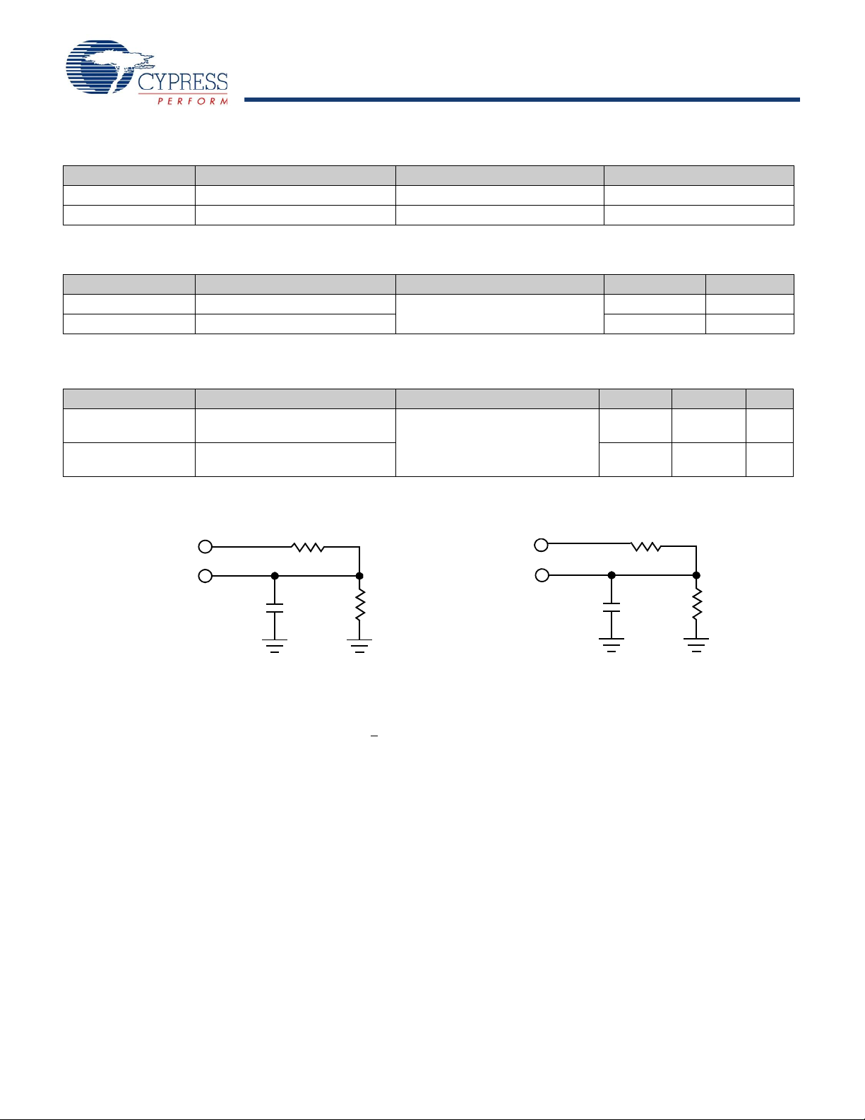
Data Retention and Endurance
3.0V
OUTPUT
5 pF
R1
R2
789Ω
3.0V
OUTPUT
30 pF
R1
R2
789Ω
577Ω
577Ω
Note
13.These parameters are only guaranteed by design and are not tested.
Parameter Description Min Unit
DATA
NV
C
R
Data Retention 20 Years
Nonvolatile STORE Operations 200 K
Capacitance
In the following table, the capacitance parameters are listed.
Parameter Description Test Conditions Max Unit
C
IN
C
OUT
Input Capacitance TA = 25°C, f = 1 MHz,
Output Capacitance 14 pF
[13]
V
= 0 to 3.0V
CC
14 pF
Thermal Resistance
In the following table, the thermal resistance parameters are listed.
Parameter Description Test Conditions 44 TSOP II 54 TSOP II Unit
Θ
Θ
JA
JC
Thermal Resistance
(Junction to Ambient)
Thermal Resistance
(Junction to Case)
Figure 6. AC Test Loads
[13]
T est conditions follow standard test
methods and procedures for
measuring thermal impedance, in
accordance with EIA/JESD51.
31.11 30.73 °C/W
5.56 6.08 °C/W
AC Test Conditions
Input Pulse Levels....................................................0V to 3V
Input Rise and Fall Times (10% - 90%)........................ <3 ns
Input and Output Timing Reference Levels....................1.5V
Document #: 001-47378 Rev. ** Page 16 of 29
[+] Feedback
Page 17
PRELIMINARY
CY14B108K, CY14B108M
Table 6. RTC Characteristics
Note
14.From either V
RTCcap
or V
RTCbat.
Parameters Description Test Conditions Min Typ Max Units
[14]
I
BAK
V
RTCbat
V
RTCcap
RTC Backup Current Room Temperature (25oC) 300 nA
Hot Temperature (85
o
C) 450 nA
RTC Battery Pin V o ltage 1.8 3.0 3.3 V
RTC Capacitor Pin Voltage 1.5 3.0 3.6 V
tOCS RTC Oscillator Time to Start 1 2 sec
Document #: 001-47378 Rev. ** Page 17 of 29
[+] Feedback
Page 18
PRELIMINARY
CY14B108K, CY14B108M
AC Switching Characteristics
Address
Data Output
Address Valid
Previous Data Valid
Output Data Valid
t
RC
t
AA
t
OHA
Notes
15.WE
must be HIGH during SRAM read cycles.
16.Device is continuously selected with CE
, OE and BHE / BLE LOW.
17.Measured ±200 mV from steady state output voltage.
18.If WE
is LOW when CE goes LOW, the outputs remain in the high impedance state.
19.HSB
must remain HIGH during Read and Write cycles.
Parameters
Cypress
Parameters
SRAM Read Cycle
t
ACE
[15]
t
RC
[16]
t
AA
t
DOE
[16]
t
OHA
[13, 17]
t
LZCE
[13, 17]
t
HZCE
[13, 17]
t
LZOE
[13, 17]
t
HZOE
[13]
t
PU
[13]
t
PD
t
DBE
[13]
t
LZBE
[13]
t
HZBE
SRAM Write Cycle
t
WC
t
PWE
t
SCE
t
SD
t
HD
t
AW
t
SA
t
HA
[13, 17,18]
t
HZWE
[13, 17]
t
LZWE
t
BW
Alt
Parameters
t
ACS
t
RC
t
AA
t
OE
t
OH
t
LZ
t
HZ
t
OLZ
t
OHZ
t
PA
t
PS
Chip Enable Access Time 20 25 45 ns
Read Cycle Time 20 25 45 ns
Address Access Time 20 25 45 ns
Output Enable to Data Valid 10 12 20 ns
Output Hold After Address Change 3 3 3 ns
Chip Enable to Output Active 3 3 3 ns
Chip Disable to Output Inactive 8 10 15 ns
Output Enable to Output Active 0 0 0 ns
Output Disable to Output Inactive 8 10 15 ns
Chip Enable to Power Active 0 0 0 ns
Chip Disable to Power Standby 20 25 45 ns
- Byte Enable to Data Valid 10 12 20 ns
- Byte Enable to Output Active 0 0 0 ns
- Byte Disable to Output Inactive 8 10 15 ns
t
WC
t
WP
t
CW
t
DW
t
DH
t
AW
t
AS
t
WR
t
WZ
t
OW
Write Cycle Time 20 25 45 ns
Write Pulse Width 15 20 30 ns
Chip Enable To End of Write 15 20 30 ns
Data Setup to End of Write 8 10 15 ns
Data Hold After End of Write 0 0 0 ns
Address Setup to End of Write 15 20 30 ns
Address Setup to Start of Write 0 0 0 ns
Address Hold After End of Write 0 0 0 ns
Write Enable to Output Disable 8 10 15 ns
Output Active after End of Write 3 3 3 ns
- Byte Enable to End of Write 15 20 30 ns
Description
20 ns 25 ns 45 ns
Min Max Min Max Min Max
Unit
Switching Waveforms
Document #: 001-47378 Rev. ** Page 18 of 29
Figure 7. SRAM Read Cycle 1: Address Controlled
[15, 16, 19]
[+] Feedback
Page 19

PRELIMINARY
CY14B108K, CY14B108M
Switching Waveforms
Address ValidAddress
Data Output
Output Data Valid
Standby
Active
High Impedance
CE
OE
BHE, BLE
I
CC
t
HZCE
t
RC
t
ACE
t
AA
t
LZCE
t
DOE
t
LZOE
t
DBE
t
LZBE
t
PU
t
PD
t
HZBE
t
HZOE
Data Output
Data Input
Input Data Valid
High Impedance
Address ValidAddress
Previous Data
t
WC
t
SCE
t
HA
t
BW
t
AW
t
PWE
t
SA
t
SD
t
HD
t
HZWE
t
LZWE
WE
BHE, BLE
CE
Note
20.CE
or WE must be >VIH during address transitions.
Figure 8. SRAM Read Cycle 2: CE Controlled
[3, 15, 19]
Document #: 001-47378 Rev. ** Page 19 of 29
Figure 9. SRAM Write Cycle 1: WE
Controlled
[3, 18, 19, 20]
[+] Feedback
Page 20

PRELIMINARY
CY14B108K, CY14B108M
Switching Waveforms
Data Output
Data Input
Input Data Valid
High Impedance
Address Valid
Address
t
WC
t
SD
t
HD
BHE, BLE
WE
CE
t
SA
t
SCE
t
HA
t
BW
t
PWE
Data Output
Data Input
Input Data Valid
High Impedance
Address ValidAddress
t
WC
t
SD
t
HD
BHE, BLE
WE
CE
t
SCE
t
SA
t
BW
t
HA
t
AW
t
PWE
(Not applicable for RTC register writes)
Note
21.Only CE
and WE controlled writes to RTC registers are allowed. BLE pin must be held LOW before CE or WE pin goes LOW for writes to RTC register.
Figure 10. SRAM Write Cycle 2: CE Controlled
[3, 18, 19, 20]
Figure 11. SRAM Write Cycle 3: BHE and BLE Controlled
[5, 18, 19, 20, 21]
Document #: 001-47378 Rev. ** Page 20 of 29
[+] Feedback
Page 21

PRELIMINARY
CY14B108K, CY14B108M
AutoStore/Power Up RECALL
V
SWITCH
V
HDIS
V
VCCR ISE
t
STORE
t
STORE
t
HHHD
t
HHHD
t
DELAY
t
DELAY
t
LZHSB
t
LZHSB
t
HRECALL
t
HRECALL
HSB OUT
Autostore
POWER-
UP
RECALL
Read & Write
Inhibited
(
RWI)
POWER-UP
RECALL
Read & Write
BROWN
OUT
Autostore
POWER-UP
RECALL
Read & Write
POWER
DOWN
Autostore
Note
23
Note
23
Note
26
Notes
22.t
HRECALL
starts from the time VCC rises above V
SWITCH.
23.If an SRAM write has not taken place since the last nonvolatile cycle, no AutoStore or Hardware STORE takes place.
24.On a Hardware STORE, Software STORE / RECALL, AutoStore Enable / Disable and AutoStore initiation, SRAM operation continues to be enabled for time t
DELAY
.
25.Read and Write cycles are ignored during STORE, RECALL, and while VCC is below V
SWITCH.
26.HSB pin is driven HIGH to VCC only by internal 100 kΩ resistor, HSB driver is disabled.
Parameters Description
[13]
[22]
Power Up RECALL Duration 20 20 20 ms
[23]
STORE Cycle Duration 8 8 8 ms
[24]
Time Allowed to Complete SRAM Cycle 20 25 25 ns
Low Voltage Trigger Level 2.65 2.65 2.65 V
VCC Rise Time 150 150 150 μs
HSB Output Driver Disable Voltage 1.9 1.9 1.9 V
HSB To Output Active Time 5 5 5 μs
HSB High Active Time 500 500 500 ns
t
HRECALL
t
STORE
t
DELAY
V
SWITCH
t
VCCRISE
V
HDIS
t
LZHSB
t
HHHD
Switching Waveforms
20 ns 25 ns 45 ns
Min Max Min Max Min Max
Figure 12. AutoStore or Power Up RECALL
Unit
[25]
Document #: 001-47378 Rev. ** Page 21 of 29
[+] Feedback
Page 22

PRELIMINARY
CY14B108K, CY14B108M
Software Controlled STORE and RECALL Cycle
t
RC
t
RC
t
SA
t
CW
t
CW
t
SA
t
HA
t
LZCE
t
HZCE
t
HA
t
HA
t
HA
t
DELAY
t
STORE/tRECALL
t
HHHD
t
LZHSB
High Impedance
Address #1 Address #6Address
CE
OE
HSB(STOREonly)
DQ (DATA)
RWI
t
RC
t
RC
t
SA
t
CW
t
CW
t
SA
t
HA
t
LZCE
t
HZCE
t
HA
t
HA
t
HA
t
DELAY
Address #1 Address #6Address
CE
OE
DQ (DATA)
t
SS
27.The software sequence is clocked with CE
controlled or OE controlled reads.
28.The six consecutive addresses must be read in the order listed in Table 2. WE
must be HIGH during all six consecutive cycles.
29.This is the amount of time it takes to take action on a soft sequence command. Vcc power must remain HIGH to effectively register command.
30.Commands such as STORE and RECALL lock out I/O until operation is complete which further increases this time. See the specific co mmand.
In the following table, the software controlled STORE and RECALL cycle parameters are listed.
Parameters Description
t
RC
t
SA
t
CW
t
HA
t
RECALL
[31, 32]
t
SS
STORE/RECALL Initiation Cycle Time 20 25 45 ns
Address Setup Time 0 0 0 ns
Clock Pulse Width 152030 ns
Address Hold Time 0 0 0 ns
RECALL Duration 200 200 200 μs
Soft Sequence Processing Time 100 100 100 μs
20 ns 25 ns 45 ns
Min Max Min Max Min Max
Switching Waveforms
Figure 13. CE and OE Controlled Software STORE and RECALL Cycle
[27, 28]
Unit
[28]
Figure 14. AutoStore Enable and Disable Cycle
Document #: 001-47378 Rev. ** Page 22 of 29
[+] Feedback
Page 23

PRELIMINARY
CY14B108K, CY14B108M
Hardware STORE Cycle
.
Address #1 Address #6 Address #1 Address #6
Soft Sequence
Command
t
SS
t
SS
CE
Address
V
CC
t
SA
t
CW
Soft Sequence
Command
t
CW
Notes
31.This is the amount of time it takes to take action on a soft sequence command. Vcc power must remain HIGH to eff ectively register command.
32.Commands such as STORE and RECALL lock out I/O until operation is complete which further increases this time. See the specific command.
Parameters Description
t
DHSB
t
PHSB
HSB To Output Active Time when write latch not set 20 25 25 ns
Hardware STORE Pulse Width 15 15 15 ns
Switching Waveforms
Write latch set
t
PHSB
HSB (IN)
t
DELAY
HSB (OUT)
DQ (Data Out)
RWI
Write latch not set
t
PHSB
HSB (IN)
HSB (OUT)
t
DELAY
20 ns 25 ns 45 ns
Min Max Min Max Min Max
Figure 15. Hardware STORE Cycle
t
STORE
HSB pin is driven high to V
100kOhm resistor,
HSB driver is disabled
SRAM is disabled as long as HSB (IN) is driven low
t
DHSB
t
DHSB
[23]
t
LZHSB
t
HHHD
only by Internal
CC
Unit
RWI
[31, 32]
Figure 16. Soft Sequence Processing
Document #: 001-47378 Rev. ** Page 23 of 29
[+] Feedback
Page 24

PRELIMINARY
CY14B108K, CY14B108M
Truth Table For SRAM Operations
HSB should remain HIGH for SRAM Operations.
For x8 Configuration
CE WE OE Inputs and Outputs
H X X High Z Deselect/Power Down Standby
L H L Data Out (DQ
–DQ7); Read Active
0
L H H High Z Output Disabled Active
L L X Data in (DQ
–DQ7); Write Active
0
For x16 Configuration
CE WE OE BHE
[3]
H X X X X High-Z Deselect/Power Down Standby
L X X H H High-Z Output Disabled Active
L H L L L Data Out (DQ
L H L H L Data Out (DQ
L H L L H Data Out (DQ
L H H L L High-Z Output Disabled Active
L H H H L High-Z Output Disabled Active
L H H L H High-Z Output Disabled Active
L L X L L Data In (DQ
L L X H L Data In (DQ
L L X L H Data In (DQ
BLE
[3]
Inputs and Outputs
–DQ
DQ
8
DQ
–DQ7 in High-Z
0
DQ
–DQ
8
–DQ7 in High-Z
DQ
0
[2]
[2]
–DQ15) Read Active
0
–DQ7);
0
in High-Z
15
–DQ15);
8
–DQ15) Write Active
0
–DQ7);
0
in High-Z
15
–DQ15);
8
Read Active
Read Active
Write Active
Write Active
Mode Power
Mode Power
Document #: 001-47378 Rev. ** Page 24 of 29
[+] Feedback
Page 25

PRELIMINARY
CY14B108K, CY14B108M
Part Numbering Nomenclature
Option:
T - Tape & Reel
Blank - Std.
Speed:
20 - 20 ns
25 - 25 ns
Data Bus:
K - x8 + RTC
M - x16 + RTC
Density:
108 - 8 Mb
Voltage:
B - 3.0V
Cypress
CY14 B 108 K ZS P 20 X C T
NVSRAM
14 - AutoStore + Software STORE + Hardware STORE
Temperature:
C - Commercial (0 to 70°C)
I - Industrial (–40 to 85°C)
Pb-Free
Package:
ZS - TSOP II
P - 54 Pin
Blank - 44 Pin
45 - 45 ns
Document #: 001-47378 Rev. ** Page 25 of 29
[+] Feedback
Page 26

PRELIMINARY
CY14B108K, CY14B108M
Ordering Information
Speed
(ns)
20 CY14B108K-ZS20XCT 51-85087 44-pin TSOPII Commercial
CY14B108K-ZS20XC 51-85087 44-pin TSOPII
CY14B108K-ZS20XIT 51-85087 44-pin TSOPII Industrial
CY14B108K-ZS20XI 51-85087 44-pin TSOPII
CY14B108M-ZSP20XCT 51-85160 54-pin TSOPII Commercial
CY14B108M-ZSP20XC 51-85160 54-pin TSOPII
CY14B108M-ZSP20XIT 51-85160 54-pin TSOPII Industrial
CY14B108M-ZSP20XI 51-85160 54-pin TSOPII
25 CY14B108K-ZS25XCT 51-85087 44-pin TSOPII Commercial
CY14B108K-ZS25XC 51-85087 44-pin TSOPII
CY14B108K-ZS25XIT 51-85087 44-pin TSOPII Industrial
CY14B108K-ZS25XI 51-85187 44-pin TSOPII
CY14B108M-ZSP25XCT 51-85160 54-pin TSOPII Commercial
CY14B108M-ZSP25XC 51-85160 54-pin TSOPII
CY14B108M-ZSP25XIT 51-85160 54-pin TSOPII Industrial
CY14B108M-ZSP25XI 51-85160 54-pin TSOPII
45 CY14B108K-ZS45XCT 51-85087 44-pin TSOPII Commercial
CY14B108K-ZS45XC 51-85087 44-pin TSOPII
CY14B108K-ZS45XIT 51-85087 44-pin TSOPII Industrial
CY14B108K-ZS45XI 51-85187 44-pin TSOPII
CY14B108M-ZSP45XCT 51-85160 54-pin TSOPII Commercial
CY14B108M-ZSP45XC 51-85160 54-pin TSOPII
CY14B108M-ZSP45XIT 51-85160 54-pin TSOPII Industrial
CY14B108M-ZSP45XI 51-85160 54-pin TSOPII
All parts are Pb-free. The above table contains Preliminary information. Contact your local Cypress sales representative for availability of these parts.
Ordering Code
Package
Diagram
Package Type
Operating
Range
Document #: 001-47378 Rev. ** Page 26 of 29
[+] Feedback
Page 27
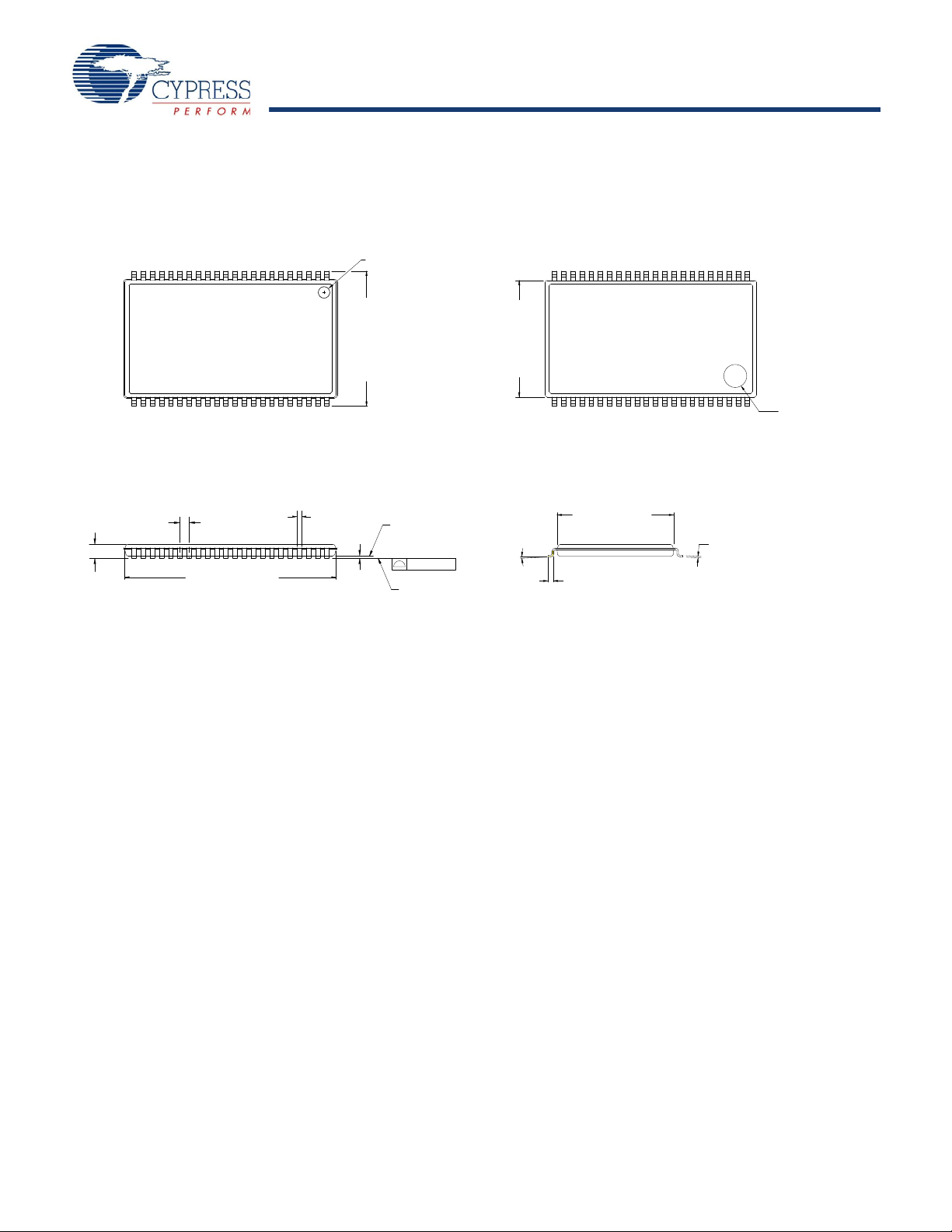
PRELIMINARY
CY14B108K, CY14B108M
Package Diagrams
MAX
MIN.
DIMENSION IN MM (INCH)
11.938 (0.470)
PLANE
SEATING
PIN 1 I.D.
44
1
18.517 (0.729)
0.800 BSC
0°-5°
0.400(0.016)
0.300 (0.012)
EJECTOR PIN
R
G
OKE
A
X
S
11.735 (0.462)
10.058 (0.396)
10.262 (0.404)
1.194 (0.047)
0.991 (0.039)
0.150 (0.0059)
0.050 (0.0020)
(0.0315)
18.313 (0.721)
10.058 (0.396)
10.262 (0.404)
0.597 (0.0235)
0.406 (0.0160)
0.210 (0.0083)
0.120 (0.0047)
BASE PLANE
0.10 (.004)
22
23
TOP VIEW BOTTOM VIEW
51-85087 *A
Figure 17. 44-Pin TSOP II (51-85087)
Document #: 001-47378 Rev. ** Page 27 of 29
[+] Feedback
Page 28

PRELIMINARY
CY14B108K, CY14B108M
Package Diagrams
51-85160 **
(continued)
Figure 18. 54-Pin TSOP II (51-85160)
Document #: 001-47378 Rev. ** Page 28 of 29
[+] Feedback
Page 29

PRELIMINARY
CY14B108K, CY14B108M
Document History Page
Document Title: CY14B108K/CY14B108M 8 Mbit (1024K x 8/512K x 16) nvSRAM with Real Time Clock
Document Number: 001-47378
Rev . ECN No.
Orig. of
Change
Submission
Date
Description of Change
** 2681767 GVCH/PYRS 04/01/09 New Data Sheet
Sales, Solutions, and Legal Information
Worldwide Sales and Design Support
Cypress maintains a worldwide network of offices, solution centers, manufacturer’s representatives, and distributors. T o find the office
closest to you, visit us at cypress.com/sales.
Products
PSoC psoc.cypress.com
Clocks & Buffers clocks.cypress.com
Wireless wireless.cypress.com
Memories memory.cypress.com
Image Sensors image.cypress.com
PSoC Solutions
General psoc.cypress.com/solutions
Low Power/Low Voltage psoc.cypress.com/low-power
Precision Analog psoc.cypress.com/precision-analog
LCD Drive psoc.cypress.com/lcd-drive
CAN 2.0b psoc.cypress.com/can
USB psoc.cypress.com/usb
© Cypress Semiconductor Corporation, 2009. The information contained herein is subject to change without notice. Cypress Semiconductor Corporation assumes no responsibility for the use of any
circuitry other than circuitry embodied in a Cypress product. Nor does it convey or imply any license under patent or other rights. Cypress products are not warranted nor intended to be used for medical,
life support, life saving, critical control or safety applications, unless pursuant to an express written agreement with Cypress. Furthermore, Cypress does not author ize its products for use as critic al
components in life-support systems where a malfunction or failure may reasonably be expected to result in significant injury to the user. The inclusion of Cypress products in life-support systems
application implies that the manufacturer assumes all risk of such use and in doing so indemnifies Cypress against all charges.
Any Source Code (software and/or firmware) is owned by Cypress Semiconductor Corporation (Cypress) and is protected by and subject to worldwide patent protection (United States and foreign),
United States copyrigh t laws and interna tional tr eaty pr ovision s. Cypr ess here by gra nt s to lic ensee a p erson al, no n-excl usive , non- tran sferabl e license to copy, use, modify, create derivative works of,
and compile the Cypress Source Code and derivative works for the sole purpose of creating custom software and or firmware in support of licensee product to be used only in conju nction with a Cypress
integrated circuit as specified in the ap plicable agr eement. Any reprod uction, modificati on, translation, co mpilation, or re presentatio n of this Source Code except as spe cified above is prohibited wi thout
the express written permission of Cypress.
Disclaimer: CYPRESS MAKES NO WARRANTY OF ANY KIND, EXPRESS OR IMPLIED, WITH REGARD TO THIS MATERIAL, INCLUDING, BUT NOT LIMITED TO, THE IMPLIED WARRANTIES
OF MERCHANTABILITY AND FITNESS FOR A PARTICULAR PURPOSE. Cypress reserves the right to make changes without further notice to the materials described herein. Cypress does not
assume any liability arising out of the app licati on or us e of an y product or circ uit de scrib ed herei n. Cypr ess does n ot auth orize it s product s for use a s critical component s in life-suppo rt systems where
a malfunction or failure may reasonably be expected to result in significant injury to the user. The inclusion of Cypress’ product in a life-support systems application implies that the manufacturer
assumes all risk of such use and in doing so indemnifies Cypress against all charges.
Use may be limited by and subject to the applicable Cypress software license agreement.
Document #: 001-47378 Rev. ** Revised April 01, 2009 Page 29 of 29
AutoStore and QuantumTrap are registered trademarks of Cypress Semiconductor Corporation. All products and company names mentioned in this document are the trademarks of their respective
holders.
[+] Feedback
 Loading...