

Page 1

CapSense® Design Guide
AN66308 - CY8CMBR2044
Doc. No. 001-66308 Rev. *F
Cypress Semiconductor
198 Champion Court
San Jose, CA 95134-1709
Phone (USA): 800.858.1810
Phone (Intnl): 408.943.2600
http://www.cypress.com
Page 2

Copyrights
Copyrights
© Cypress Semiconductor Corporation, 2010-2017. This document is the property of Cypress Semiconductor Corporation and its subsidiaries,
including Spansion LLC (“Cypress”). This document, including any software or firmware included or referenced in this d ocument (“Software”), is
owned by Cypress under the intellectual property laws and treaties of the United States and other countries worldwide. Cypress reserves all rights
under such laws and treaties and does not, except as specifically stated in this paragraph, grant any license under its patents, copyrights,
trademarks, or other intellectual property rights. If the Software is not accompanied by a license agreement and you do not otherwise have a written
agreement with Cypress governing the use of the Software, then Cypress hereby grants you a personal, non-exclusive, nontransferable license
(without the right to sublicense) (1) under its copyright rights in the Software (a) for Software provided in source code form, to modify and reproduce
the Software solely for use with Cypress hardware products, only internally within your organization, and (b) to distribute the Software in binary code
form externally to end users (either directly or indirectly through resellers and distributors), solely for use on Cypress hardware product units, and (2)
under those claims of Cypress’s patents that are infringed by the Software (as provided by Cypress, unmodified) to make, use, distribute, and import
the Software solely for use with Cypress hardware products. Any other use, reproduction, modification, translation, or compilation of the Software is
prohibited.
TO THE EXTENT PERMITTED BY APPLICABLE LAW, CYPRESS MAKES NO WARRANTY OF ANY KIND, EXPRESS OR IMPLIED, WITH
REGARD TO THIS DOCUMENT OR ANY SOFTWARE OR ACCOMPANYING HARDWARE, INCLUDING, BUT NOT LIMITED TO, THE IMPLIED
WARRANTIES OF MERCHANTABILITY AND FITNESS FOR A PARTICULAR PURPOSE. To the extent permitted by applicable law, Cypress
reserves the right to make changes to this document without further notice. Cypress does not assume any liability arising out of the application or
use of any product or circuit described in this document. Any information provided in this document, including any sample design information or
programming code, is provided only for reference purposes. It is the responsibility of the user of this document to properly design, program, and test
the functionality and safety of any application made of this information and any resulting product. Cypress products are not designed, intended, or
authorized for use as critical components in systems designed or intended for the operation of weapons, weapons systems, nuclear installations, lifesupport devices or systems, other medical devices or systems (including resuscitation equipment and surgical implants), pollution control or
hazardous substances management, or other uses where the failure of the device or system could cause personal injury, death, or property damage
(“Unintended Uses”). A critical component is any component of a device or system whose failure to perform can be reasonably expected to cause
the failure of the device or system, or to affect its safety or effectiveness. Cypress is not liable, in whole or in part, and you shall and hereby do
release Cypress from any claim, damage, or other liability arising from or related to all Unintended Uses of Cypress products. You shall indemnify
and hold Cypress harmless from and against all claims, costs, damages, and other liabilities, including claims for personal injury or death, arising
from or related to any Unintended Uses of Cypress products.
Cypress, the Cypress logo, Spansion, the Spansion logo, and combinations thereof, WICED, PSoC, CapSense, EZ-USB, F-RAM, and Traveo are
trademarks or registered trademarks of Cypress in the United States and other countries. For a more complete list of Cypress trademarks, visit
cypress.com. Other names and brands may be claimed as property of their respective owners
AN66308 - CY8CMBR2044 CapSense® Design GuideDoc. No. 001-66308 Rev. *F 2
Page 3

Contents
1. Introduction .................................................................................................................................................................... 5
1.1 Abstract ................................................................................................................................................................. 5
1.2 Cypress’s CapSense Documentation Ecosystem .................................................................................................. 5
1.3 CY8CMBR2044 CapSense Express™ Device Features ....................................................................................... 7
1.4 Document Conventions ......................................................................................................................................... 9
2. CapSense Technology ................................................................................................................................................ 10
2.1 CapSense Fundamentals .................................................................................................................................... 10
2.2 Capacitive Sensing Method ................................................................................................................................. 11
2.2.1 CapSense Sigma-Delta (CSD) ............................................................................................................... 11
2.3 SmartSense Auto-Tuning .................................................................................................................................... 13
2.3.1 Process Variation.................................................................................................................................... 13
2.3.2 Reduced Design Cycle Time .................................................................................................................. 13
3. CapSense Schematic Design ..................................................................................................................................... 15
3.1 CY8CMBR2044 Configuration Options ............................................................................................................... 15
3.1.1 CapSense Buttons (CSx) ........................................................................................................................ 15
3.1.2 General-Purpose Outputs (GPOx) .......................................................................................................... 15
3.1.3 Modulation Capacitor (C
3.1.4 Button Auto Reset (ARST) ...................................................................................................................... 16
3.1.5 Toggle ON/OFF ...................................................................................................................................... 16
3.1.6 Flanking Sensor Suppression (FSS) ....................................................................................................... 17
3.1.7 LED ON Time ......................................................................................................................................... 18
3.1.8 System Diagnostics ................................................................................................................................ 19
3.1.9 Scan Rate/Sleep ..................................................................................................................................... 21
3.1.10 Serial Debug Data Out ............................................................................................................................ 22
3.2 Design Toolbox .................................................................................................................................................... 25
3.2.1 General Layout Guidelines ................................ ..................................................................................... 25
3.2.2 Layout Estimator ..................................................................................................................................... 26
3.2.3 CP, Power Consumption and Response Time Calculator ....................................................................... 27
3.2.4 Design Validation .................................................................................................................................... 28
) .................................................................................................................. 15
MOD
4. Electrical and Mechanical Design Considerations ................................................................................................... 30
4.1 Overlay Selection ................................................................................................................................................ 30
AN66308 - CY8CMBR2044 CapSense® Design Guide, Doc. No. 001-66308 Rev. *F 3
4.1.1 Bonding Overlay to PCB ......................................................................................................................... 31
Page 4

Contents
4.2 ESD Protection .................................................................................................................................................... 31
4.2.1 Prevent ................................................................................................................................................... 31
4.2.2 Redirect .................................................................................................................................................. 31
4.2.3 Clamp ..................................................................................................................................................... 31
4.3 Electromagnetic Compatibility (EMC) Considerations ......................................................................................... 32
4.3.1 Radiated Interference ............................................................................................................................. 32
4.3.2 Conducted Immunity and Emissions ....................................................................................................... 32
4.4 PCB Layout Guidelines ....................................................................................................................................... 32
5. Low-Power Design Considerations ........................................................................................................................... 33
5.1 System Design Recommendations ...................................................................................................................... 33
5.2 Calculating Average Power ................................................................................................................................. 33
5.2.1 Button Scan Rate (TR) ............................................................................................................................ 33
5.2.2 Scan Time (TS) ....................................................................................................................................... 34
5.2.3 Average Current in NO TOUCH State (I
5.2.4 Average Current in TOUCH State (I
5.2.5 Average Standalone Current (I
5.2.6 Average Current (I
5.2.7 Average Power (P
) ............................................................................................................................ 35
AVE
) ............................................................................................................................. 36
AVE
AVE_T
) ..................................................................................................... 35
AVE_SA
5.2.8 Example Calculation ............................................................................................................................... 36
5.3 Sleep Modes........................................................................................................................................................ 37
5.3.1 Low-Power Sleep Mode .......................................................................................................................... 37
5.3.2 Deep Sleep Mode ................................................................................................................................ ... 37
) ....................................................................................... 35
AVE_NT
) ............................................................................................... 35
6. Resources .................................................................................................................................................................... 38
6.1 Website ............................................................................................................................................................... 38
6.2 Datasheet ............................................................................................................................................................ 38
6.3 Design Toolbox .................................................................................................................................................... 38
6.4 Multi-Chart ........................................................................................................................................................... 38
6.5 Design Support .................................................................................................................................................... 39
7. Appendix ...................................................................................................................................................................... 40
7.1 Schematic Example ............................................................................................................................................. 40
7.1.1 Schematic 1: Four Buttons with Four GPOs ........................................................................................... 40
7.1.2 Schematic 2: Three Buttons with Advanced Features enabled .............................................................. 42
Acronyms ...................................................................................................................................................................... 43
Glossary ................................................................................................................................................................................ 44
Revision History ................................................................................................................................................................... 50
Document Revision History ........................................................................................................................................... 50
AN66308 - CY8CMBR2044 CapSense® Design Guide, Doc. No. 001-66308 Rev. *F 4
Page 5

1. Introduction
Abstract
This document describes how to implement capacitive sensing functionality using Cypress’s CapSense
CY8CMBR2044 device. The following topics are covered in this guide:
Features of the CY8CMBR2044
CapSense principles of operation
Configuration options of the CY8CMBR2044 device
Using the Design Toolbox with the CY8CMBR2044
System electrical and mechanical design considerations for the CY8CMBR2044
Low-power design considerations for the CY8CMBR2044
Additional resources and support for designing CapSense into your system
®
Express
Cypress’s CapSense Documentation Ecosystem
Figure 1-1 and Table 1-1 summarize the CapSense documentation ecosystem. These resources allow the
implementers to quickly access the information they need to complete a CapSense product design. Figure 1-1 shows
a typical product design cycle with capacitive sensing; this document covers the topics highlighted in green. Table 1-1
offers links to supporting documents for each of the numbered tasks in Figure 1-1.
AN66308 - CY8CMBR2044 CapSense® Design Guide, Doc. No. 001-66308 Rev. *F 5
Page 6

Introduction
3. Select CapSense device based on
required functionality
2. Specify system requirements and
characteristics
11. Preproduction build (prototype)
12. Test and evaluate system functionality and
CapSense performance
Meets
specifications?
13. Production
Yes
No
= Topics covered in this document
1. Understand CapSense technology
4. Mechanical
Design
5. Schematic
capture and
PCB layout
Design for CapSense
9. Programming PSoC
†
10. CapSense
Configuration*
6. PSoC Designer project
creation†
7. Firmware
development†
8. CapSense tuning†
*
†
= Applicable to MBR family of devices only
= Applicable to programmable devices only
Figure 1-1. Typical CapSense Product Design Flow
AN66308 - CY8CMBR2044 CapSense® Design Guide, Doc. No. 001-66308 Rev. *F 6
Page 7

Introduction
Numbered Design Task of
Figure 1-1
Supporting Cypress CapSense® Documentation
1
Getting Started with CapSense
2
CY8CMBR2044 Device Datasheet
3
Getting Started with CapSense
4
This document
5
This document
6
Not applicable for CY8CMBR2044
7
Not applicable for CY8CMBR2044
8
Not applicable for CY8CMBR2044
9
Not applicable for CY8CMBR2044
10
This document
11
This document
Table 1-1. Cypress Documents That Support Numbered Design Tasks of Figure 1-1
CY8CMBR2044 CapSense Express™ Device Features
Cypress’s CY8CMBR2044 is an ultra-low power device that can quickly and easily add CapSense capacitive touch
sensing to your user interface. This device uses hardware to perform system configuration, eliminating the need for
software tools, firmware development and device programming. The features of the device are listed as follows. For
more details, see CY8CMBR2044 Configuration Options.
Easy-to-use capacitive button controller
Four-button solution configurable through Hardware straps
No software tools or programming required
Four general-purpose outputs (GPOs)
GPOs are linked to CapSense buttons
GPOs support direct LED drive
Robust noise performance
Specifically designed for superior noise immunity to external radiated and conducted noise
Low radiated noise emission
SmartSense™ Auto-Tuning
Saves time and effort in device tuning
CapSense parameters dynamically set in runtime
Maintains optimal button performance even in noisy environment
AN66308 - CY8CMBR2044 CapSense® Design Guide, Doc. No. 001-66308 Rev. *F 7
Page 8

Introduction
Wide parasitic capacitance CP range ( 5 pF – 40 pF)
System Diagnostics of CapSense buttons – reports any faults at device power-up
Button shorted to Ground
Button shorted to VDD
Button to button short
Improper value of modulator capacitor (C
Parasitic capacitance (CP) out of range
Advanced features
Toggle ON/OFF feature on GPOs
Flanking Sensor Suppression (FSS) provides robust sensing even with closely spaced buttons
Configurable LED ON Time after button release
Button output reset if touched for excessive time
User-controlled Button Scan Rate
Serial Debug Data output
o Simplifies production line testing and system debug
Wider operating voltage range
1.71 V to 5.5 V – ideal for both regulated and unregulated battery applications
Low power consumption
Supply current in run mode as low as 15 µAa per button
Deep Sleep current: 100 nA
Industrial temperature range: –40 ºC to + 85 ºC
16-pad Quad Flat No leads (QFN) package (3 mm x 3 mm x 0.6 mm)
a
Power consumption calculated with 1.7% touch time, 500 ms Button Scan Rate, Cp of each button < 19 pF
MOD
)
AN66308 - CY8CMBR2044 CapSense® Design Guide, Doc. No. 001-66308 Rev. *F 8
Page 9

Introduction
Convention
Usage
Courier New
Displays file locations, user entered text, and source code:
C:\ ...cd\icc\
Italics
Displays file names and reference documentation:
Read about the sourcefile.hex file in the PSoC Designer User Guide.
[Bracketed, Bold]
Displays keyboard commands in procedures:
[Enter] or [Ctrl] [C]
File > Open
Represents menu paths:
File > Open > New Project
Bold
Displays commands, menu paths, and icon names in procedures:
Click the File icon and then click Open.
Times New Roman
Displays an equation:
2 + 2 = 4
Text in gray boxes
Describes Cautions or unique functionality of the product.
Document Conventions
AN66308 - CY8CMBR2044 CapSense® Design Guide, Doc. No. 001-66308 Rev. *F 9
Page 10
2. CapSense Technology
CY8CMBR2044
C
MOD
Sensor
Capacitors
CapSense Fundamentals
CapSense is a touch sensing technology that works by measuring the capacitance of each input pin on the
CapSense controller that has been designated as a sensor. As shown in Figure 2-1, the total capacitance on each of
the sensor pins can be modeled as equivalent lumped capacitors with values of C
sensors. Circuitry internal to the CY8CMBR2044 device converts the magnitude of each CX into a digital code that is
stored for post-processing. A modulating capacitor, C
C
will be discussed in more detail in Capacitive Sensing Method.
MOD
, is used by the CapSense controller’s internal circuitry.
MOD
Figure 2-1. CapSense Implementation in a CY8CMBR2044 Device
through C
X,1
for a design with n
X,n
Each sensor input pin is connected to a sensor pad by traces, vias, or both, as necessary. A nonconductive overlay is
required to cover the sensor pad and constitutes the product’s touch interface. When a finger comes into contact with
the overlay, the conductivity and mass of the body effectively introduces a grounded conductive plane parallel to the
sensor pad. This action is represented in Figure 2-2. This arrangement constitutes a parallel plate capacitor, whose
capacitance is given by the following equation:
Equation 1
Where:
CF = The capacitance affected by a finger in contact with the overlay over a sensor
ε
= Free space permittivity
0
ε
= Dielectric constant (relative permittivity) of overlay
r
A = Area of finger and sensor pad overlap
D = Overlay thickness
AN66308 - CY8CMBR2044 CapSense® Design Guide, Doc. No. 001-66308 Rev. *F 10
Page 11

CapSense Technology
Figure 2-2. Section of typical CapSense PCB with the Sensor being activated by a Finger
In addition to the parallel plate capacitance, a finger in contact with the overlay causes electric field fringing between
itself and other conductors in the immediate vicinity. Typically, the effect of these fringing fields is minor, and it can
usually be ignored.
Even without a finger touching the overlay, the sensor input pin has some parasitic capacitance (CP). CP results from
the combination of the CapSense controller internal parasitic and electric field coupling among the sensor pad,
traces, and vias, and other conductors in the system, such as ground plane, other traces, any metal in the product’s
chassis or enclosure, and so on. The CapSense controller measures the total capacitance (CX) connected to a
sensor pin.
When a finger is not touching a sensor, use this equation:
Equation 2
With a finger on the sensor, CX equals the sum of CP and CF:
Equation 3
In general, CP is an order of magnitude greater than CF. CP usually ranges from 10 pF to 20 pF, but in extreme cases
it can be as high as 40 pF. CF usually ranges from 0.1 pF to 0.4 pF.
Capacitive Sensing Method
CY8CMBR2044 device supports the CapSense Sigma Delta (CSD) with SmartSense™ Auto-Tuning for converting
sensor capacitance (CX) into digital counts. The CSD method is described in the following sections.
CapSense Sigma-Delta (CSD)
The CSD method in the CY8CMBR2044 device incorporates CX into a switched capacitor circuit, as shown in
Figure 2-3. The sensor (CX) is alternatively connected to GND and the Analog MUX (AMUX) bus by the non-
overlapping switches Sw1 and Sw2, respectively. Sw1 and Sw2 are driven by a precharge clock to bleed a current
(ISENSOR) from the AMUX bus. The magnitude of ISENSOR is directly proportional to the magnitude of CX. The sigma-
delta converter samples AMUX bus voltage and generates a modulating bit stream that controls the constant current
source (IDAC), which charges AMUX such that the average AMUX bus voltage is maintained at VREF. The sensor
bleeds off the charge ISENSOR from the modulating capacitor (CMOD). CMOD, in combination with Rbus, forms a low-pass
filter that attenuates precharge switching transients at the sigma-delta converter input.
AN66308 - CY8CMBR2044 CapSense® Design Guide, Doc. No. 001-66308 Rev. *F 11
Page 12

CapSense Technology
Cx
isensor
Sigma-Delta
Converter
Precharge
Clock
Cmod
High-Z
input
Sw1
Sw2
CY8CMBR2044
Gnd
= External Connection
AMUX
Bus
Vref
Rbus
Gnd
IDAC
Figure 2-3. CSD Block Diagram
In maintaining the average AMUX voltage at a steady state value (VREF), the sigma-delta converter matches the
average charge current (IDAC) to ISENSOR by controlling the bit stream duty cycle. The sigma-delta converter stores the
bit stream over the duration of a sensor scan, and the accumulated result is a digital output value, known as raw
count, which is directly proportional to CX. This raw count is interpreted by high-level algorithms to resolve the sensor
state. Figure 2-4 plots the CSD raw counts from a number of consecutive scans during which the sensor is touched
and then released by a finger. As explained in CapSense Fundamentals, the finger touch causes CX to increase by
CF, which in turn causes raw counts to increase proportionally. By comparing the shift in steady state raw count level
to a predetermined threshold, the high-level algorithms can determine whether the sensor is in an ON (Touch) or OFF
(No Touch) state.
Figure 2-4. CSD Raw Counts During a Finger Touch
AN66308 - CY8CMBR2044 CapSense® Design Guide, Doc. No. 001-66308 Rev. *F 12
Page 13
CapSense Technology
SmartSense Auto-Tuning
Tuning the touch-sensing user interface is a critical step in ensuring proper system operation and a pleasant user
experience. In the typical design flow, the button interface is tuned in the initial design phase, during system
integration, and before the production ramp. Because it’s an iterative process, tuning can be time-consuming.
SmartSense Auto-Tuning was developed to simplify the user interface development cycle. It is easy to use and
reduces the design cycle time by eliminating the hassles of further manual tuning in prototype and manufacturing
stages. SmartSense Auto-Tuning tunes each CapSense button automatically at power up and then monitors and
maintains optimum button performance during runtime. This technology adapts for manufacturing variation in PCBs
and overlays and automatically tunes out noise from sources such as LCD inverters, AC lines, and switch-mode
power supplies.
Process Variation
SmartSense Auto-Tuning for the CY8CMBR2044 is designed to work with button parasitic capacitance in the range of
5 pF to 40 pF, (typical button CP values range from 10 pF to 20 pF). The sensitivity parameter for each button is set
automatically, based on the characteristics of that particular button. The parameter improves the yield in mass
production because every button maintains a consistent response regardless of the CP variation (from 5 pF to 40 pF)
between the buttons. Parasitic capacitance of the individual buttons can vary due to PCB layout and trace length,
PCB manufacturing process variation, or vendor-to-vendor PCB variation within a multi-sourced supply chain. The
sensitivity of a button depends on its parasitic capacitance; higher CP values decrease sensitivity, resulting in
decreased finger touch signal amplitude. In some cases, a change in CP detunes the system, resulting in unfavorable
button performance (either too sensitive or insensitive) or even a nonoperational button. In either situation, you must
retune the system and, in some cases, you need to requalify the user interface subsystem. SmartSense Auto-Tuning
resolves these issues.
SmartSense Auto-Tuning makes platform designs possible. For example, consider the capacitive touch sensing
multimedia keys on a laptop computer; the spacing between the buttons depends on the size of the laptop and the
keyboard layout. In this example, the wide-screen machine has larger spaces between the buttons than a standardscreen model would. The additional space means increased trace length between the button and the CapSense
controller. The bigger trace length, in turn, leads to a higher parasitic capacitance of the button. As a result, the
parasitic capacitance of the CapSense buttons can vary in different models of the same platform design. Though the
buttons’ functionality is identical for all of the laptop models, the buttons must be tuned for each model. SmartSense
Auto-Tuning lets you do platform designs using the recommended practices shown in the PCB Layout in Getting
Started with CapSense.
Figure 2-5. Design of Laptop Multi-Media Keys for 21-inch Model
Figure 2-6. Design of Laptop Multi-Media Keys for 15-inch Model with Same Functionality and Button Size
Reduced Design Cycle Time
When you design a capacitive button interface, the most time-consuming tasks are firmware development, layout,
and button tuning. With a typical touch-sensing controller, the button must be retuned when the same design is
ported to different models or when the mechanical dimensions change in the PCB or the button PCB layout. A design
with SmartSense™ Auto-Tuning meets these challenges because it needs no firmware development, no manual
tuning, and no retuning. In addition, SmartSense™ Auto-Tuning speeds up a typical design cycle. Figure 2-7
compares the design cycles of a typical touch-sensing controller and a SmartSense™ Auto-Tuning-based design.
AN66308 - CY8CMBR2044 CapSense® Design Guide, Doc. No. 001-66308 Rev. *F 13
Page 14

CapSense Technology
Feasibility
Study
Schematics
Design
PCB Layout
Design
Mechanical Design
Review
System
Integration
Retuning for any
changes
Tuning process
Production Fine
Tuning
Design
Validation
Production
Typical capacitive user interface Design Cycle
Firmware
Development
Feasibility
Study
Schematics
Design
PCB Layout
Design
Mechanical Design
Review
System
Integration
Design
Validation
Production
CapSense® Express with SmartSense™ Auto-Tuning based
capacitive user interface Design Cycle
Device
Configuration
Figure 2-7. Typical Capacitive Interface Design Cycle Comparison
AN66308 - CY8CMBR2044 CapSense® Design Guide, Doc. No. 001-66308 Rev. *F 14
Page 15

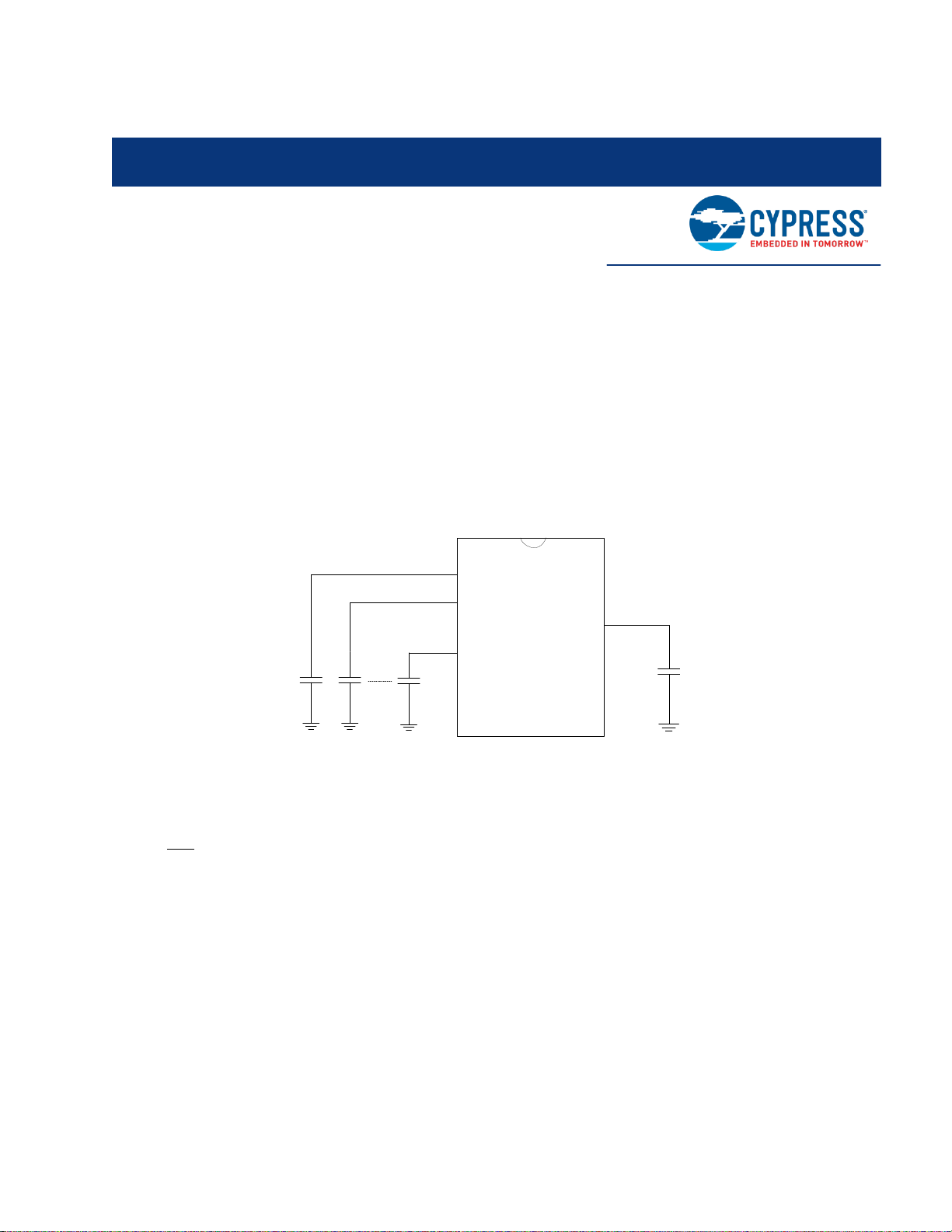
3. CapSense Schematic Design
CY8CMBR2044 Configuration Options
Cypress’s CY8CMBR2044 enables you to implement capacitive touch sensing using only hardware. This section
provides an overview of the CapSense controller pins and how to configure them.
Figure 3-1. CY8CMBR2044 Pin Diagram
CapSense Buttons (CSx)
The CY8CMBR2044 controller has four capacitive sense inputs, CS0–CS3. Each capacitive button requires a
connection to one of the capacitive sense inputs. You must ground all unused CapSense (CSx) inputs pins.
General-Purpose Outputs (GPOx)
There are four active LOW outputs on the CY8CMBR2044 controller, GPO0–GPO3. Each output, GPOx, is driven by
its corresponding capacitive sensing input, CSx. You can use GPOs to directly drive LEDs or to replace mechanical
switches. GPOs are in strong drivea mode. You must leave all unused GPOs floating.
Modulation Capacitor (C
Connect a 2.2-nF (±10%) capacitor to the C
a
When a pin is in strong drive mode, it is pulled up to VDD when the output is HIGH and pulled down to Ground when the output is
LOW. The output cannot be floating.
AN66308 - CY8CMBR2044 CapSense® Design Guide, Doc. No. 001-66308 Rev. *F 15
MOD
)
pin.
MOD
Page 16

CapSense Schematic Design
ARST Pin Connection
Button Auto Reset Period
(seconds)
Ground
5
5 kΩ (10%) resistor to ground
20
VDD or floating
No Limit
CS0
GPO0
Auto Reset period
GPO0 is not driven after
Auto Reset period
Button is touched for more
than the Auto Reset period
Toggle/FSS Pin Connection
Toggle ON/OFF
FSS
Ground
Disabled
Disabled
1.5 kΩ (5%) resistor to ground
Enabled
Disabled
5.1 kΩ (5%) resistor to ground
Disabled
Enabled
VDD
Enabled
Enabled
Button Auto Reset (ARST)
Button Auto Reset determines the maximum time a GPOx is driven when CSx is continuously touched. This feature
prevents a button from getting stuck if a metal object s placed too close to it. The ARST period can be configured to
be 5 seconds or 20 seconds. The Button Auto Reset is defined in Table 3-1 and shown in Figure 3-2.
Table 3-1. ARST Pin Configuration
Figure 3-2. Button Auto Reset
After the GPOx is turned off because of Button Auto Reset feature and after the button is released, do not touch the
button for a specific amount of time (T) given, as follows:
T equals 220 ms, if the CSx input is released within 2 seconds after Button Auto Reset period is elapsed.
T equals 220 ms plus the Button Scan Rate, if the CSx input is released after 2 seconds, after Button Auto
Reset period is elapsed.
Toggle ON/OFF
When Toggle ON/OFF is enabled, the state of GPOx changes on every rising edge of CSx. Toggle ON/OFF
configuration is defined in Table 3-2 and shown in Figure 3-3.
Table 3-2. Toggle/FSS Pin Configuration
AN66308 - CY8CMBR2044 CapSense® Design Guide, Doc. No. 001-66308 Rev. *F 16
Page 17

CapSense Schematic Design
CS0
GPO0
Figure 3-3. Example of Toggle ON/OFF Feature
Flanking Sensor Suppression (FSS)
FSS helps to distinguish closely spaced buttons by allowing only one CSx to be in the TOUCH state at a time. If a
finger contacts multiple CSx buttons, only the first one to sense a TOUCH state will turn ON.
FSS also is useful when a button can produce opposite effects – for example, an interface with two buttons for
brightness control (UP or DOWN).
FSS configuration is defined in Table 3-2 and shown in Figure 3-4 and Figure 3-5.
Figure 3-4. FSS Implementation, Single Button Touched
AN66308 - CY8CMBR2044 CapSense® Design Guide, Doc. No. 001-66308 Rev. *F 17
Page 18

CapSense Schematic Design
CS0
GPO0
LED ON Time
Figure 3-5. FSS Implementation, Multiple Buttons Touched
LED ON Time
LED ON Time specifies the duration for which GPOx is driven low after CSx is released. LED ON Time can range
from 0 ms to 2000 ms.
Figure 3-6. LED ON Timing
The LED ON Time duration, D, is configurable from the Delay pin. For different values of resistors connected to the
Delay pin, the time can be varied. The resistor, R
Equation 4
Where:
D is a multiple of 20 ms
Table 3-3 provides some example values for the Delay pin configuration and the resulting LED ON Time. R
resistor tolerance should be less than 1 percent.
, is defined by Equation 4.
DELAY
DELAY
AN66308 - CY8CMBR2044 CapSense® Design Guide, Doc. No. 001-66308 Rev. *F 18
Page 19

CapSense Schematic Design
R
DELAY
(Ω)
Approx. LED ON Time
(ms)
Grounded
0
120
20
200
40
280
60 … …
7960
1980
8040
2000
> 8040
2000
Pulled to VDD
2000
Floating
2000
CS0
GPO0
CS1
GPO1
Start LED ON Time
Counter
Restart LED ON
Time Counter
Reset LED ON
Time Counter
LED ON Time
Table 3-3. R
Value for LED ON Time
DELAY
Place R
between the Delay pin and ground. LED ON Time varies from device to device. It is ±12% accurate at
DELAY
room temperature and ±18% accurate at a temperature range of -40 °C to +85 °C.
If a Button Auto Reset is triggered for CSx, LED ON Time is not applied on GPOx. LED ON Time is disabled if Toggle
ON/OFF is enabled.
LED ON Time applies only to one GPOx at a time, meaning the LED ON Time counter resets every time a CSx
transitions to a NO TOUCH state. Figure 3-7 illustrates how LED ON Time operates: CS1 resets the LED ON Time
counter, causing GPO0 to turn OFF prematurely.
Figure 3-7. LED ON Timing Diagram for Multiple Buttons
System Diagnostics
A built-in Power-on Self Test (POST) mechanism performs some tests at power-on reset (POR), which can be useful
in production testing. If any button fails these tests, a 5 ms pulse is sent out on the corresponding GPO within 175 ms
after POR. The following tests are performed on all of the buttons:
AN66308 - CY8CMBR2044 CapSense® Design Guide, Doc. No. 001-66308 Rev. *F 19
Page 20

CapSense Schematic Design
CY8CMBR2044
Button
shorting
CY8CMBR2044
Button
shorting
V
DD
CY8CMBR2044
Button
shorting
Button
Button Shorted to Ground
If any button is found to be shorted to ground, it is disabled.
Figure 3-8. Button Shorted to Ground
Button Shorted to VDD
If any button is found to be shorted to VDD, it is disabled.
Figure 3-9. Button Shorted to VDD
Button to Button Short
If two or more buttons are found to be shorted to each other, all of these buttons are disabled.
Figure 3-10. Button to Button Short
Improper Value of C
Recommended value of C
AN66308 - CY8CMBR2044 CapSense® Design Guide, Doc. No. 001-66308 Rev. *F 20
MOD
is 2.2 nF ± 10%.
MOD
Page 21

CapSense Schematic Design
5ms pulse
GPO3
GPO2
GPO1
(High)
GPO0
(High)
5ms pulse
If the value of C
is found to be less than 1 nF or greater than 4 nF, all the buttons are disabled.
MOD
Button CP > 40 pF
If the parasitic capacitance (CP) of any button is found to be more than 40 pF, that button is disabled.
Figure 3-11.ExampleShowing CS), CS1 Passing the POST and CS2, CS3 Failing
Scan Rate/Sleep
Use this pin to set the button scan rate and sleep mode operation of the CY8CMBR2044. Do not leave this pin
floating.
Button Scan Rate
The button scan rate specifies the time between successive button scans by the device. An external resistor
determines the button scan rate for the CY8CMBR2044. You can use the Cp, Power Consumption and Response
Time Calculator to determine the scan rate resistor value or Table 3-4.The button scan rate is configurable from
20 ms to 531 ms.
AN66308 - CY8CMBR2044 CapSense® Design Guide, Doc. No. 001-66308 Rev. *F 21
Page 22

CapSense Schematic Design
Table 3-4. Resistor Value Selection for Button Scan Rate
Button Scan Rate varies from device to device. It is ±12 percent accurate at room temperature and ±18 percent
accurate at a temperature range of -–40 °C to +85 °C.
Sleep Mode
There are two possible configurations:
1. Connect the Button Scan Rate resistor to ground. This enables low power sleep mode
2. Connect the Button Scan Rate resistor to an external Master (host processor) and configure the host pin to be
HIGH (VDD). This enables deep sleep mode.
Further details are in the Sleep Modes section.
Serial Debug Data Out
Serial Debug Data reports firmware revision, CapSense status, GPO status, raw count, baseline, difference count,
and parasitic capacitance for all buttons. When Serial Debug Data is enabled this information is output on a single
CSx pin. To enable Serial Data Out, pull down the CSx pin where you want the serial data to appear with a 5.6-kΩ
resistor with a 5-percent tolerance. If more than one CSx pin is pulled down, debug data is sent out only on one CSx
pin. The priority is:
CS0 > CS1 > CS2 > CS3
The Cypress Multi-Chart Tool can be used to view the data. The Serial Debug Data is sent by the device in the order
according to Table 3-5. The MultiChart tool arranges the data in the format as shown in Table 3-6.
Serial data is sent out with ~115,200 baud rate.
For designs using less than four CapSense buttons, the unused CS pin should be selected for Serial Debug Data.
For designs using all four CapSense buttons, use two CSx pins for Serial Debug Data. For example, pull down CS0
with a 5.6-kΩ resistor and read the data for CS1, CS2, and CS3. Next, pull down CS1 with a 5.6-kΩ resistor and read
the data for CS0, CS2, and CS3.
AN66308 - CY8CMBR2044 CapSense® Design Guide, Doc. No. 001-66308 Rev. *F 22
Page 23

CapSense Schematic Design
Byte
Data
Notes
0
0x0D
Dummy data for multi chart
1
0x0A
2
0x00 – 3
FW_Revision
Firmware Revision
4
0x00 – 5
CS0_Cp
CS0 parasitic capacitance (pF) in Hex
6
CS0_RawCount_MSB
Unsigned 16-bit integer
7
CS0_RawCount_LSB
8
CS1_RawCount_MSB
Unsigned 16-bit integer
9
CS1_RawCount_LSB
10
CS2_RawCount_MSB
Unsigned 16-bit integer
11
CS2_RawCount_LSB
12
CS3_RawCount_MSB
Unsigned 16-bit integer
13
CS3_RawCount_LSB
14
CS_Status
Gives CapSense button status, least significant bit (LSB) contains CS0 status
15
GPO_Status
Gives GPO status, LSB contains GPO0 status
16
0x00 – 17
CS1_Cp
CS1 parasitic capacitance (pF) in Hex
18
CS0_Baseline_MSB
Unsigned 16-bit integer
19
CS0_Baseline_LSB
20
CS1_Baseline_MSB
Unsigned 16-bit integer
21
CS1_Baseline_LSB
22
CS2_Baseline_MSB
Unsigned 16-bit integer
23
CS2_Baseline_LSB
24
CS3_Baseline_MSB
Unsigned 16-bit integer
25
CS3_Baseline_LSB
26
0x00 – 27
CS2_Cp
CS2 parasitic capacitance (pF) in Hex
28
0x00 – 29
CS3_cp
CS3 parasitic capacitance (pF) in Hex
30
CS0_DiffCount_MSB
Unsigned 16-bit integer
31
CS0_DiffCount_LSB
32
CS1_DiffCount_MSB
Unsigned 16-bit integer
33
CS1_DiffCount_LSB
34
CS2_DiffCount_MSB
Unsigned 16-bit integer
35
CS2_DiffCount_LSB
36
CS3_DiffCount_MSB
Unsigned 16-bit integer
Table 3-5. Serial Data Output Sent by CY8CMBR2044
AN66308 - CY8CMBR2044 CapSense® Design Guide, Doc. No. 001-66308 Rev. *F 23
Page 24

CapSense Schematic Design
Byte
Data
Notes
37
CS3_DiffCount_LSB
38
0x00
Dummy data for MultiChart
39
0xFF
40
0xFF
#
Raw Count Array
Baseline Array
Signal array
MSB
LSB
MSB
LSB
MSB
LSB
0
0x00
FW_Revision
CS_Status
GPO_Status
0x00
CS2_Cp
1
0x00
CS0_Cp
0x00
CS1_Cp
0x00
CS3_Cp
2
CS0_RawCount
CS0_Baseline
CS0_DiffCount
3
CS1_RawCount
CS1_Baseline
CS1_DiffCount
4
CS2_RawCount
CS2_Baseline
CS2_DiffCount
5
CS3_RawCount
CS3_Baseline
CS3_DiffCount
Table 3-6. Serial Debug Data Arranged in Multichart
AN66308 - CY8CMBR2044 CapSense® Design Guide, Doc. No. 001-66308 Rev. *F 24
Page 25

CapSense Schematic Design
Design Toolbox
The Design Toolbox helps you to design a CY8CMBR2044 CapSense solution. It offers basic information about the
board layout and feature settings and recommends whether the design is fit for mass production.
General Layout Guidelines
The table below summarizes the layout guidelines for the CY8CMBR2044. These guidelines are discussed in
Electrical and Mechanical Electrical and Mechanical Design Considerations of this guide. For a thorough treatment of
this material, see Getting Started with CapSense, Section 3.7.
Figure 3-12. Design Layout Recommendations
AN66308 - CY8CMBR2044 CapSense® Design Guide, Doc. No. 001-66308 Rev. *F 25
Page 26

CapSense Schematic Design
Layout Estimator
The Layout Estimator provides the minimum button size and maximum trace length recommendation based on the
intended end-system requirements and industrial design. The inputs include the overlay material, overlay thickness,
and trace capacitance of circuit board material. Refer to Figure 3-13, Table B, to learn the dielectric constants for
different overlay materials and the trace capacitance per unit length for different PCBs. Table A calculates the
minimum button diameter and maximum trace length for the design, based on three relative ranges of system noise.
Low, medium, and high noise is a relative figure of merit to help you with button development. Noise conditions can
vary button to button based on the end-system environment. If the noise conditions are unknown, use medium noise
conditions as the starting point. The actual noise seen at each button will be determined in the design validation step
described in Design Validation.
Use the outputs of this sheet to guide the sensor board layout process and then check the design prior to prototyping
with the CP, Power Consumption and Response Time Calculator sheet as detailed Cp, Power Consumption and
Response Time Calculator.
Figure 3-13. Layout Estimator
Inputs:
Overlay thickness
Overlay dielectric constant
Capacitance of trace per inch of board
Outputs:
Recommended minimum button diameter and maximum trace length for different noise conditions
Button to ground clearance
Note The button diameter of each button can be different in the design based on whether the noise varies button to
button.
AN66308 - CY8CMBR2044 CapSense® Design Guide, Doc. No. 001-66308 Rev. *F 26
Page 27

CapSense Schematic Design
CP, Power Consumption and Response Time Calculator
After the board layout has been completed, use this calculator to check the design before building the button board
prototype. To verify the CP value of each button, insert the button diameters and trace lengths into Table A. After you
enter the information, the toolbox confirms whether each button is within the specified CP range of 5 pF to 40 pF. The
power calculator in Table B is used to optimize power consumption. Power consumption is a function of the button
scan rate, which is set by the resistor value on the ScanRate/Sleep pin. Refer to Section 3.4 Scan Rate and Table
3-4. Table C outputs the button response time based on the inputs in Tables A and B.
Figure 3-14. CP, Power Consumption and Response Time Calculator
Inputs:
Button diameter and trace length of CS0–CS3 as designed in layout
Button Scan rate resistor value
The percentage of time a finger is on the buttons
Outputs:
Parasitic Capacitance (CP) for each sensor. Confirms whether the CP values are within the specified range
of 5 pF to 40 pF
Power consumption per button
Button response time
After you have built and tested the prototype board, you can determine the actual parasitic capacitance (CP) and
noise condition (noise count) of each button according to the Section 3.1.10 Serial Debug Data Out. Use this
information and the Design Validation Sheet to validate the design, as detailed in Section 0Design Validation
AN66308 - CY8CMBR2044 CapSense® Design Guide, Doc. No. 001-66308 Rev. *F 27
Page 28

CapSense Schematic Design
Design Validation
After you have prototyped and tested the button board, use the Serial Debug Data Out test mode (Section 3.1.10
Serial Debug Data Out) to capture the raw count, baseline, difference count, and parasitic capacitance for all buttons.
To enter this information into Table C of the sheet, follow these steps –
1. Enable the Serial Debug Data Out feature by connecting a 5.6 kΩ resistor to GND on any CSx pin.
2. Power on the device and connect the CSx pin to the computer through a COM/RS232 port.
3. Open MultiChart and configure it as following –
a. Select PORT - <Specify PORT number>
b. Port Speed – 115200
c. Visible points – 1000
d. Log file name – “C:\MultiChart log\CY8CMBR2044.csv”
To know more about MultiChart, see AN2397 – CapSense Data Viewing Tools
4. Click on “Enable/disable log-file”. This will automatically store the data to the log file. Log this data for at least
300 samples.
5. Click on “Enable/disable log-file”. This will stop logging the data.
6. Open the log file once. The toolbox will automatically be updated with the relevant data.
Table A shows the various design parameter values, taken up from the previous sheets, so that you need not enter
any data in this sheet. This sheet provides a pass/fail grade for the prototype board. If your design fails, you can
redesign your system by entering new values in Table A and further recommendations/results will be given. If your
design passes, leave the “New value” column in Table A blank.
Figure 3-15 Design Validation
Inputs:
If the design passes – None
If the design fails –
o New overlay thickness, overlay material permittivity, button diameter for each individual button, and
trace capacitance
AN66308 - CY8CMBR2044 CapSense® Design Guide, Doc. No. 001-66308 Rev. *F 28
Page 29

CapSense Schematic Design
o Button Scan Rate resistor value used in design
o Percentage of time a finger is on the buttons
Outputs:
Power consumption per button
Design change recommendations. The Design Toolbox provides recommendations based on the actual
values from the design if the button size or trace lengths are outside of best design practices.
If the button board does not pass, the Design Toolbox will provide recommendations. There are four areas that can
be changed to remedy a failing design: button size, trace length, overlay material, and overlay thickness. Changing
the button size or trace length requires a board spin, while changing the overlay material or thickness, or both, may
be a shorter path to a passing design. The best solution depends on where the project stands in the development
process and the end-system requirements. The Design Toolbox will guide you to a passing outcome.
AN66308 - CY8CMBR2044 CapSense® Design Guide, Doc. No. 001-66308 Rev. *F 29
Page 30

4. Electrical and Mechanical Design
Considerations
Material
Breakdown Voltage (V/mm)
Min. Overlay Thickness at 12 kV (mm)
Air
1200–2800
10
Wood – dry
3900
3
Glass – common
7900
1.5
Glass – Borosilicate (Pyrex®))
13,000
0.9
PMMA Plastic (Plexiglas®)
13,000
0.9
ABS
16,000
0.8
Polycarbonate (Lexan®)
16,000
0.8
Formica
18,000
0.7
FR-4
28,000
0.4
PET Film – (Mylar®)
280,000
0.04
Polymide film – (Kapton®)
290,000
0.04
When designing a capacitive touch sense technology into your application it is crucial to keep in mind that the
CapSense device exists within a larger framework. Careful attention to every detail, including PCB layout, user
interface, and end-user operating environment, leads to robust and reliable system performance. For in-depth
information, refer to Getting Started with CapSense.
Overlay Selection
In CapSense Equation 1 was presented for finger capacitance
Where:
ε
= Free space permittivity
0
ε
= Dielectric constant of overlay
r
A = Area of finger and sensor pad overlap
D = Overlay thickness
To increase the CapSense signal strength, choose an overlay material with a higher dielectric constant, decrease the
overlay thickness, and increase the button diameter. The Design Toolbox helps you to design a robust and reliable
CY8CMBR2044 solution, as discussed in the chapter CapSense Schematic Design.
Table 4-1. Overlay Material Dielectric Strength
Conductive material cannot be used as an overlay because it interferes with the electric field pattern. Therefore, do
not use paint containing metal particles.
AN66308 - CY8CMBR2044 CapSense® Design Guide, Doc. No. 001-66308 Rev. *F 30
Page 31

Electrical and Mechanical Design Considerations
ESD Protection device
Input
Capacitance
Leakage
Current
Contact
Discharge
maximum limit
Air Discharge
maximum limit
Manufacturer
Part Number
Littlefuse
SP723
5 pF
2 nA
8 kV
15 kV
Vishay
VBUS05L1-DD1
0.3 pF
0.1 µA <
±15 kV
±16 kV
NXP
NUP1301
0.75 pF
30 nA
8 kV
15 kV
Bonding Overlay to PCB
Because the dielectric constant of air is very low, an air gap between the overlay and the button degrades the
performance of the button. To eliminate the gap, use a nonconductive adhesive to bond the overlay to the CapSense
PCB. A transparent acrylic adhesive film from 3M™ called 200MP is qualified for use in CapSense applications. This
special adhesive is dispensed from paper-backed tape rolls (3M™ product numbers 467MP and 468MP).
ESD Protection
Robust ESD tolerance is a natural byproduct of thoughtful system design. By considering how the contact discharge
occurs in your end product, particularly in your user interface, you can withstand an 18-kV discharge event without
incurring any damage to the CapSense controller.
CapSense controller pins can withstand a direct 12-kV event. In most cases, the overlay material provides sufficient
ESD protection for the controller pins. Table 4-1 lists the thickness of various overlay materials required to protect the
CapSense sensors from a 12-kV discharge as specified in IEC 61000-4-2. If the overlay material does not provide
sufficient ESD protection, apply countermeasures in the following order: Prevent, Redirect, Clamp.
Prevent
Make sure all paths on the touch surface have a breakdown voltage greater than potential high-voltage contacts. In
addition, design your system to maintain an appropriate distance between the CapSense controller and possible
sources of ESD. If it is not possible to maintain adequate distance, place a protective layer of a high-breakdownvoltage material between the ESD source and CapSense controller. One layer of 5-mil-thick Kapton® tape will
withstand 18 kV.
Redirect
If your product is densely packed, it may not be possible to prevent the discharge event. In this case, you can protect
the CapSense controller by controlling where the discharge occurs. Place a guard ring on the perimeter of the circuit
board that is connected to chassis ground. As recommended in PCB Layout Guidelines, using a hatched ground
plane around the button can redirect the ESD event away from the button and CapSense controller.
Clamp
Because CapSense sensors are purposely placed in close proximity to the touch surface, it may not be practical to
redirect the discharge path. In this case, consider including series resistors or special-purpose ESD protection
devices.
The recommended series resistance value is 560 Ω.
A more effective method is to provide special-purpose ESD protection devices on the vulnerable traces. Note that
ESD protection devices for CapSense need to be low in capacitance. Table 4-2 lists devices recommended for use
with CapSense controllers.
Table 4-2. Low-Capacitance ESD Protection Devices Recommended for CapSense
AN66308 - CY8CMBR2044 CapSense® Design Guide, Doc. No. 001-66308 Rev. *F 31
Page 32

Electrical and Mechanical Design Considerations
Button CP Range
Sink Current Limit per GPO
Sink Current Limit for Device
5 pF ≤ CP ≤ 12 pF
25 mA
120 mA
12 pF ≤ CP ≤ 21 pF
20 mA
20 mA
21 pF ≤ CP ≤ 40 pF
6 mA
6 mA
Electromagnetic Compatibility (EMC) Considerations
Radiated Interference
Radiated electrical energy can influence system measurements and potentially influence the operation of the
processor core. The interference enters the CY8CMBR2044 chip at the PCB level, through CapSense button traces
and any other digital or analog inputs. The Layout guidelines for minimizing the effects of RF interference follow:
Ground Plane: provide a ground plane on the PCB
Series Resistor: place series resistors within 10 mm of the CapSense controller pins
o The recommended series resistance for CapSense input lines is 560 Ω
Trace Length: Minimize trace length whenever possible
Current Loop Area: Minimize the return path for current. To reduce the impact of parasitic capacitance,
hatched ground is given within 1 cm of the buttons and traces, instead of solid fill.
RF Source Location: Partition systems with noise sources, such as LCD inverters and switched-mode
power supplies (SMPS), to keep the interference separated from CapSense inputs. Shielding the power
supply is another common technique to prevent interference.
Conducted Immunity and Emissions
Noise entering a system through interconnections with other systems is referred to as conducted noise. Examples
include power and communication lines. Because the CapSense controllers are low-power devices, you must avoid
conducted emissions. The following guidelines will help to reduce conducted emission and immunity:
Use decoupling capacitors.
Add a bidirectional filter on the input to the system power supply. This is effective for both conducted
emissions and immunity. A pi-filter can prevent power supply noise from effecting sensitive parts and also
prevent the switching noise of the part itself from coupling back onto the power planes.
If the CapSense controller PCB is connected to the power supply by a cable, minimize the cable length and
consider using a shielded cable.
To filter out high-frequency noise, place a ferrite bead around power supply or communication lines.
PCB Layout Guidelines
The Design Toolbox will help you design a robust and reliable CY8CMBR2044 CapSense PCB layout, as discussed
in Section 0
If your design uses the GPOs to sink current to the CapSense controller, and there is a lot of noise in the CapSense
system, use series resistors on all of the GPOs to limit sink current. Sink current limit is determined by the maximum
button CP in your design at 5 V, as show in Table 4-3.
Table 4-3. GPO Sink Current Limit for Low Output Voltage
Detailed PCB layout guidelines are available in Getting Started with CapSense, Section 3.7.
AN66308 - CY8CMBR2044 CapSense® Design Guide, Doc. No. 001-66308 Rev. *F 32
Page 33

5. Low-Power Design Considerations
System Design Recommendations
Cypress’s CY8CMBR2044 is designed to meet the low-power requirements of battery powered applications.
To minimize power consumption, take these steps:
Ground all unused CapSense inputs
Minimize CP using the design guidelines in Getting Started with CapSense, Section 3.7.1.
Reduce supply voltage
Use a higher Button Scan Rate or Deep Sleep operating mode, refer to Button Scan Rate.
Calculating Average Power
The Design Toolbox, which is the tool of choice, automates the power consumption calculations described in the
following sections. The average power consumed by the CY8CBMR2044 is determined by calculating the parameters
below:
1. Button Scan rate, TR
2. Scan time, TS
3. Average current in a NO TOUCH state, I
4. Average current in a TOUCH state, I
5. Average standalone current, I
6. Average current, I
7. Average power, P
AVE
AVE
AVE_SA
AVE_T
Button Scan Rate (TR)
Control the Button Scan rate though the external resistor connected to the ScanRate/Sleep pin of CY8CMBR2044.
The following equation provides the approximate scan rate:
Where:
R = value of external resistor (in ohms).
Refer to Table 3-4 to find the appropriate resistor value.
Response Time (T
Selecting the Scan Rate means balancing the response time and power consumption requirements of your
application.
Equation 5
)
RES
AVE_NT
AN66308 - CY8CMBR2044 CapSense® Design Guide, Doc. No. 001-66308 Rev. *F 33
Page 34

Low-Power Design Considerations
CP
(pF)
Button Sensitivity Constant
(K)
Button connected to Ground
0
5 pF ≤ CP ≤ 10 pF
1
10 pF < CP ≤ 22 pF
2
23 pF < CP ≤ 40 pF
4
Parameter
Typ
Max
TFW
1.50 ms
1.57 ms
I
SLEEP
1.07 µA
1.5 µA
TS
From Equation 7
+5% from TYP value
TR
Table 3-4
±10 from Value
I
ACTIVE
2.67 mA
3.8 mA
Response time, T
senses a TOUCH state. The CY8CMBR2044 device has two different response times. The first is the time it takes to
respond when the device wakes up from low power mode:
Equation 6
Where:
TR = Scan Rate
And the second is the time it takes to respond to any subsequent TOUCH after it wakes up, 80 ms.
is the amount of time the CY8CMBR2044 takes to produce a valid signal on GPOx after CSx
RES,
Scan Time (TS)
Approximate scan time can be calculated using:
Where:
K
= button sensitivity constant for CSx.
CSX
TFW = Firmware execution time, from Table 5-2.
Table 5-1. Button Sensitivity Constant
Equation 7
Table 5-2. Average Current Parameters
AN66308 - CY8CMBR2044 CapSense® Design Guide, Doc. No. 001-66308 Rev. *F 34
Page 35

Low-Power Design Considerations
Average Current in NO TOUCH State (I
AVE_NT
)
Equation 8
Where:
TR = Button Scan Rate
TS = Scan time
I
= current consumed by CY8CMBR2044 during low power sleep mode, from Table 5-2
SLEEP
I
= current consumed by CY8CMBR2044 during active operation, from Table 5-2
ACTIVE
Average Current in TOUCH State (I
AVE_T
)
Equation 9
Where:
TS = Scan time
I
= current consumed by CY8CMBR2044 during low power sleep mode, from Table 5-2
SLEEP
I
= current consumed by CY8CMBR2044 during active operation, from Table 5-2
ACTIVE
Average Standalone Current (I
AVE_SA
)
Equation 10
Where
P = percentage of time CS is in the TOUCH state compared to total time CY8CMBR2044 is on
I
= average current for in the NO TOUCH state
AVG_NT
I
= average current in the TOUCH state
AVG_T
Average Current (I
AVE
)
Equation 11
Where:
T
= time device is in standalone mode
SA
TDS = time device is in deep sleep mode
AN66308 - CY8CMBR2044 CapSense® Design Guide, Doc. No. 001-66308 Rev. *F 35
Page 36

Low-Power Design Considerations
Average Power (P
Equation 12
AVE
)
Where:
I
= average current
AVE
Example Calculation
As an example of how to calculate average power, consider a CapSense user interface on a bluetooth headset with
three well-designed buttons. The CP for all three buttons is between 10 pF and 22 pF. The buttons are scanned at a
rate of 507 ms.
The scan time can be calculated using a sensor constant of 2 for all three buttons and Equation 13:
Equation 13
The average current in NO TOUCH state is calculated as follows using Equation 14 and the maximum values for
I
and I
SLEEP
The average current in TOUCH state is calculated as follows using Equation 15:
To calculate the average current, assume your headset receives 50 calls in an 8-hour business day and the user
touches a CapSense button every 20 seconds during each call. This means your design operates in a TOUCH state
about 1.8 percent of the 8 hours during which the headset is turned on. The average current consumption of the
design is calculated as follows using Equation 16:
Equation 16
Assuming this design does not utilize deep sleep mode and that it operates at 1.71 V the average power is calculated
as follows using Equation 17:
Equation 17
:
ACTIVE
Equation 14
Equation 15
AN66308 - CY8CMBR2044 CapSense® Design Guide, Doc. No. 001-66308 Rev. *F 36
Page 37

Low-Power Design Considerations
Scan all buttons with 20 ms Scan
Rate (Scan time + Sleep time)
NO button touched for
2 secs?
Yes
Scan all buttons with user defined
scan rate.
Is any button active?
Yes
No
No
Sleep Modes
Cypress’s CY8CMBR2044 can be configured to operate in either low-power sleep mode or deep sleep mode.
Low-Power Sleep Mode
When the CY8CMBR2044 device operates in low power sleep mode, the device draws 1 µA when not scanning the
CS inputs. The scan rate determines the amount of time. The behavior of CY8CMBR2044 controller in low-power
sleep mode is described in Figure 5-1.
Figure 5-1. Low-Power Sleep Mode
Because low-power sleep mode does not require a host processor to operate, it is also referred to as standalone
mode.
Deep Sleep Mode
If the CY8CMBR2044 is used in a system with a host processor, the ScanRate/Sleep control pin can be used to
operate in deep sleep mode. When the host processor provides logic high to this input pin, the CY8CMBR2044 is put
into deep sleep mode. This mode consumes 0.1 µA (typ) of current. When the host drives a GND signal to the same
input pin, the CY8CMBR2044 wakes up from sleep and operates in low-power sleep mode.
AN66308 - CY8CMBR2044 CapSense® Design Guide, Doc. No. 001-66308 Rev. *F 37
Page 38

6. Resources
Website
Visit Cypress’s CapSense Controllers website to access all of the reference material discussed in this section.
Find a variety of technical resources at the CY8CMBR2044 web page.
Datasheet
The datasheet for the CapSense CY8CMBR2044 device is available at www.cypress.com.
CY8CMBR2044
Design Toolbox
The interactive Design Toolbox will enable you to design a robust and reliable CY8CMBR2044 CapSense solution.
Watch the Design Tool Box example video on web.
Multi-Chart
Multi-Chart is a simple PC tool for real-time CapSense data viewing and logging. The application allows you to view
data from up to 48 sensors, save and print charts, and save data for later analysis in a spreadsheet.
AN66308 - CY8CMBR2044 CapSense® Design Guide, Doc. No. 001-66308 Rev. *F 38
Page 39

Resources
Design Support
To ensure the success of your CapSense solutions, Cypress has a variety of design support channels.
Knowledge Based Articles –Browse technical articles by product family or perform a search on various
CapSense topics.
CapSense Application Notes – a wide variety of application notes built on information presented in this
document.
White Papers – Learn about advanced capacitive touch interface topics.
Cypress Developer Community – Connect with the Cypress technical community and exchange information.
CapSense Product Selector Guide – See the complete product offering of Cypress CapSense product line.
Video Library – Quickly get up to speed with tutorial videos
CY8CMBR2044 Videos – Get up to speed quickly with an overview of the product features and design
toolbox.
Quality & Reliability – Cypress is committed to complete customer satisfaction. At our Quality website you
can find reliability and product qualification reports.
Technical Support – World class technical support is available on-line.
AN66308 - CY8CMBR2044 CapSense® Design Guide, Doc. No. 001-66308 Rev. *F 39
Page 40

7. Appendix
Schematic Example
Schematic 1: Four Buttons with Four GPOs
In the above schematic, the device is configured as:
CS0 – CS3 pins: 560 Ω to CapSense buttons
AN66308 - CY8CMBR2044 CapSense® Design Guide, Doc. No. 001-66308 Rev. *F 40
o Four CapSense buttons (CS0 – CS3)
Page 41

Appendix
GPO0 – GPO3 pins: LED and 560 Ω to VDD
o CapSense buttons driving four LEDs (GPO0 – GPO3)
CMOD pin: 2.2 nF to Ground
o Modulator capacitor
XRES pin: Floating
o For external reset
Toggle/FSS pin: Ground
o Toggle ON/OFF disabled
o FSS disabled
ARST pin: 5 kΩ to Ground
o Button Auto Reset enabled, Auto Reset Period = 20 seconds
Delay pin: Ground
o LED ON Time disabled
ScanRate/Sleep pin: Ground
o User configured scan rate = 20 ms
To enable Serial Debug Data output, connect a 5.6 kohm resistor on R9 or R12.
AN66308 - CY8CMBR2044 CapSense® Design Guide, Doc. No. 001-66308 Rev. *F 41
Page 42

Appendix
Schematic 2: Three Buttons with Advanced Features enabled
In the above schematic, the device is configured as:
CS0 – CS2 pins: 560 Ω to CapSense buttons; CS3 pin: Ground
o Three CapSense buttons (CS0 – CS2)
o CS3 not used in design
GPO0 – GPO2 pins: LED and 560 Ω to VDD; GPO3 floating; GPO0-GPO1 pins interfaced to Master
o CapSense buttons driving three LEDs (GPO0 – GPO2)
o GPO0, GPO1 interfaced to master for direct status read
CMOD pin: 2.2 nF to Ground
o Modulator capacitor
XRES pin: Floating
o For external reset
Toggle/FSS pin: 5.1 kΩ to Ground
o Toggle ON/OFF disabled
o FSS enabled
ARST pin: 5 kΩ to Ground
o Button Auto Reset enabled, Auto Reset period = 20 seconds
AN66308 - CY8CMBR2044 CapSense® Design Guide, Doc. No. 001-66308 Rev. *F 42
Page 43

Appendix
Acronym
Description
AC
Alternating current
ARST
Auto Reset
CF
Finger capacitance
CP
Parasitic capacitance
CS
CapSense
CSD
CapSense Sigma Delta
EMC
Electromagnetic Compatibility
ESD
Electrostatic Discharge
FSS
Flanking Sensor Suppression
GPO
General-Purpose Output
MSB
Most significant bit
LCD
Liquid Crystal Display
LED
Light-Emitting Diode
LSB
Least significant bit
PCB
Printed Circuit Board
POR
Power on Reset
POST
Power on Self-Test
RF
Radio Frequency
SMPS
Switched Mode Power Supply
Delay pin: 4 kΩ to Ground
o LED ON Time of 1000 ms
ScanRate/Sleep pin: 560 Ω to Master
o User configured scan rate = 30 ms
o Master to control device operating mode
To enable Serial Debug Data output, connect a 5.6 kohm resistor on R11.
Acronyms
AN66308 - CY8CMBR2044 CapSense® Design Guide, Doc. No. 001-66308 Rev. *F 43
Page 44

Glossary
AMUXBUS
Analog multiplexer bus available inside PSoC that helps to connect I/O pins with multiple internal analog
signals.
SmartSense™ Auto-Tuning
A CapSense algorithm that automatically sets sensing parameters for optimal performance after the
design phase and continuously compensates for system, manufacturing, and environmental changes.
Baseline
A value resulting from a firmware algorithm that estimates a trend in the Raw Count when there is no
human finger present on the sensor. The Baseline is less sensitive to sudden changes in the Raw Count
and provides a reference point for computing the Difference Count.
Button or Button Widget
A widget with an associated sensor that can report the active or inactive state (that is, only two states) of
the sensor. For example, it can detect the touch or no-touch state of a finger on the sensor.
Difference Count
The difference between Raw Count and Baseline. If the difference is negative, or if it is below Noise
Threshold, the Difference Count is always set to zero.
Capacitive Sensor
A conductor and substrate, such as a copper button on a printed circuit board (PCB), which reacts to a
touch or an approaching object with a change in capacitance.
CapSense®
Cypress’s touch-sensing user interface solution. The industry’s No. 1 solution in sales by 4x over No. 2.
CapSense Mechanical Button Replacement (MBR)
Cypress’s configurable solution to upgrade mechanical buttons to capacitive buttons, requires minimal
engineering effort to configure the sensor parameters and does not require firmware development. These
devices include the CY8CMBR3XXX and CY8CMBR2XXX families.
Centroid or Centroid Position
A number indicating the finger position on a slider within the range given by the Slider Resolution. This
number is calculated by the CapSense centroid calculation algorithm.
Compensation IDAC
A programmable constant current source, which is used by CSD to compensate for excess sensor CP.
This IDAC is not controlled by the Sigma-Delta Modulator in the CSD block unlike the Modulation IDAC.
CSD
AN66308 - CY8CMBR2044 CapSense® Design Guide, Doc. No. 001-66308 Rev. *F 44
Page 45

Glossary
CapSense Sigma Delta (CSD) is a Cypress-patented method of performing self-capacitance (also called
self-cap) measurements for capacitive sensing applications.
In CSD mode, the sensing system measures the self-capacitance of an electrode, and a change in the
self-capacitance is detected to identify the presence or absence of a finger.
Debounce
A parameter that defines the number of consecutive scan samples for which the touch should be present
for it to become valid. This parameter helps to reject spurious touch signals.
A finger touch is reported only if the Difference Count is greater than Finger Threshold + Hysteresis for a
consecutive Debounce number of scan samples.
Driven-Shield
A technique used by CSD for enabling liquid tolerance in which the Shield Electrode is driven by a signal
that is equal to the sensor switching signal in phase and amplitude.
Electrode
A conductive material such as a pad or a layer on PCB, ITO, or FPCB. The electrode is connected to a
port pin on a CapSense device and is used as a CapSense sensor or to drive specific signals associated
with CapSense functionality.
Finger Threshold
A parameter used with Hysteresis to determine the state of the sensor. Sensor state is reported ON if the
Difference Count is higher than Finger Threshold + Hysteresis, and it is reported OFF if the Difference
Count is below Finger Threshold – Hysteresis.
Ganged Sensors
The method of connecting multiple sensors together and scanning them as a single sensor. Used for
increasing the sensor area for proximity sensing and to reduce power consumption.
To reduce power when the system is in low-power mode, all the sensors can be ganged together and
scanned as a single sensor taking less time instead of scanning all the sensors individually. When the
user touches any of the sensors, the system can transition into active mode where it scans all the sensors
individually to detect which sensor is activated.
PSoC supports sensor-ganging in firmware, that is, multiple sensors can be connected simultaneously to
AMUXBUS for scanning.
Gesture
Gesture is an action, such as swiping and pinch-zoom, performed by the user. CapSense has a gesture
detection feature that identifies the different gestures based on predefined touch patterns. In the
CapSense component, the Gesture feature is supported only by the Touchpad Widget.
Guard Sensor
Copper trace that surrounds all the sensors on the PCB, similar to a button sensor and is used to detect a
liquid stream. When the Guard Sensor is triggered, firmware can disable scanning of all other sensors to
prevent false touches.
Hatch Fill or Hatch Ground or Hatched Ground
AN66308 - CY8CMBR2044 CapSense® Design Guide, Doc. No. 001-66308 Rev. *F 45
Page 46

Glossary
While designing a PCB for capacitive sensing, a grounded copper plane should be placed surrounding
the sensors for good noise immunity. But a solid ground increases the parasitic capacitance of the sensor
which is not desired. Therefore, the ground should be filled in a special hatch pattern. A hatch pattern has
closely-placed, crisscrossed lines looking like a mesh and the line width and the spacing between two
lines determine the fill percentage. In case of liquid tolerance, this hatch fill referred as a shield electrode
is driven with a shield signal instead of ground.
Hysteresis
A parameter used to prevent the sensor status output from random toggling due to system noise, used in
conjunction with the Finger Threshold to determine the sensor state. See Finger Threshold.
IDAC (Current-Output Digital-to-Analog Converter)
Programmable constant current source available inside PSoC, used for CapSense and ADC operations.
Liquid Tolerance
The ability of a capacitive sensing system to work reliably in the presence of liquid droplets, streaming
liquids or mist.
Linear Slider
A widget consisting of more than one sensor arranged in a specific linear fashion to detect the physical
position (in single axis) of a finger.
Low Baseline Reset
A parameter that represents the maximum number of scan samples where the Raw Count is abnormally
below the Negative Noise Threshold. If the Low Baseline Reset value is exceeded, the Baseline is reset
to the current Raw Count.
Manual-Tuning
The manual process of setting (or tuning) the CapSense parameters.
Matrix Buttons
A widget consisting of more than two sensors arranged in a matrix fashion, used to detect the presence
or absence of a human finger (a touch) on the intersections of vertically and horizontally arranged
sensors.
If M is the number of sensors on the horizontal axis and N is the number of sensors on the vertical axis,
the Matrix Buttons Widget can monitor a total of M x N intersections using ONLY M + N port pins.
When using the CSD sensing method (self-capacitance), this Widget can detect a valid touch on only one
intersection position at a time.
Modulation Capacitor (CMOD)
An external capacitor required for the operation of a CSD block in Self-Capacitance sensing mode.
Modulator Clock
A clock source that is used to sample the modulator output from a CSD block during a sensor scan. This
clock is also fed to the Raw Count counter. The scan time (excluding pre and post processing times) is
given by (2N – 1)/Modulator Clock Frequency, where N is the Scan Resolution.
Modulation IDAC
AN66308 - CY8CMBR2044 CapSense® Design Guide, Doc. No. 001-66308 Rev. *F 46
Page 47

Glossary
Modulation IDAC is a programmable constant current source, whose output is controlled (ON/OFF) by the
sigma-delta modulator output in a CSD block to maintain the AMUXBUS voltage at V
. The average
REF
current supplied by this IDAC is equal to the average current drawn out by the sensor capacitor.
Mutual-Capacitance
Capacitance associated with an electrode (say TX) with respect to another electrode (say RX) is known
as mutual capacitance.
Negative Noise Threshold
A threshold used to differentiate usual noise from the spurious signals appearing in negative direction.
This parameter is used in conjunction with the Low Baseline Reset parameter.
Baseline is updated to track the change in the Raw Count as long as the Raw Count stays within
Negative Noise Threshold, that is, the difference between Baseline and Raw count (Baseline – Raw
count) is less than Negative Noise Threshold.
Scenarios that may trigger such spurious signals in a negative direction include: a finger on the sensor on
power-up, removal of a metal object placed near the sensor, removing a liquid-tolerant CapSenseenabled product from the water; and other sudden environmental changes.
Noise (CapSense Noise)
The variation in the Raw Count when a sensor is in the OFF state (no touch), measured as peak-to-peak
counts.
Noise Threshold
A parameter used to differentiate signal from noise for a sensor. If Raw Count – Baseline is greater than
Noise Threshold, it indicates a likely valid signal. If the difference is less than Noise Threshold, Raw
Count contains nothing but noise.
Overlay
A non-conductive material, such as plastic and glass, which covers the capacitive sensors and acts as a
touch-surface. The PCB with the sensors is directly placed under the overlay or is connected through
springs. The casing for a product often becomes the overlay.
Parasitic Capacitance (CP)
Parasitic capacitance is the intrinsic capacitance of the sensor electrode contributed by PCB trace,
sensor pad, vias, and air gap. It is unwanted because it reduces the sensitivity of CSD.
Proximity Sensor
A sensor that can detect the presence of nearby objects without any physical contact.
Radial Slider
A widget consisting of more than one sensor arranged in a specific circular fashion to detect the physical
position of a finger.
Raw Count
The unprocessed digital count output of the CapSense hardware block that represents the physical
capacitance of the sensor.
Refresh Interval
The time between two consecutive scans of a sensor.
Scan Resolution
Resolution (in bits) of the Raw Count produced by the CSD block.
AN66308 - CY8CMBR2044 CapSense® Design Guide, Doc. No. 001-66308 Rev. *F 47
Page 48

Glossary
Scan Time
Time taken for completing the scan of a sensor.
Self-Capacitance
The capacitance associated with an electrode with respect to circuit ground.
Sensitivity
The change in Raw Count corresponding to the change in sensor capacitance, expressed in counts/pF.
Sensitivity of a sensor is dependent on the board layout, overlay properties, sensing method, and tuning
parameters.
Sense Clock
A clock source used to implement a switched-capacitor front-end for the CSD sensing method.
Sensor
See Capacitive Sensor.
Sensor Auto Reset
A setting to prevent a sensor from reporting false touch status indefinitely due to system failure, or when a
metal object is continuously present near the sensor.
When Sensor Auto Reset is enabled, the Baseline is always updated even if the Difference Count is
greater than the Noise Threshold. This prevents the sensor from reporting the ON status for an indefinite
period of time. When Sensor Auto Reset is disabled, the Baseline is updated only when the Difference
Count is less than the Noise Threshold.
Sensor Ganging
See Ganged Sensors.
Shield Electrode
Copper fill around sensors to prevent false touches due to the presence of water or other liquids. Shield
Electrode is driven by the shield signal output from the CSD block. See Driven-Shield.
Shield Tank Capacitor (CSH)
An optional external capacitor (CSH Tank Capacitor) used to enhance the drive capability of the CSD
shield, when there is a large shield layer with high parasitic capacitance.
Signal (CapSense Signal)
Difference Count is also called Signal. See Difference Count.
Signal-to-Noise Ratio (SNR)
The ratio of the sensor signal, when touched, to the noise signal of an untouched sensor.
Slider Resolution
A parameter indicating the total number of finger positions to be resolved on a slider.
Touchpad
A Widget consisting of multiple sensors arranged in a specific horizontal and vertical fashion to detect the
X and Y position of a touch.
Trackpad
See Touchpad.
Tuning
AN66308 - CY8CMBR2044 CapSense® Design Guide, Doc. No. 001-66308 Rev. *F 48
Page 49

Glossary
The process of finding the optimum values for various hardware and software or threshold parameters
required for CapSense operation.
V
REF
Programmable reference voltage block available inside PSoC used for CapSense and ADC operation.
Widget
A user-interface element in the CapSense component that consists of one sensor or a group of similar
sensors. Button, proximity sensor, linear slider, radial slider, matrix buttons, and touchpad are the
supported widgets.
AN66308 - CY8CMBR2044 CapSense® Design Guide, Doc. No. 001-66308 Rev. *F 49
Page 50

Revision History
Document Title: AN66308 - CY8CMBR2044 CapSense® Design Guide
Document Number: 001-66308
Revision
Issue Date
Origin of
Change
Description of Change
**
12/30/2010
ANBA
New Design Guide.
*A
03/03/2011
ANBA
Multiple chapter enhancements for content and reader clarity.
*B
06/01/2012
UDYG
Multiple chapter enhancements for content and reader clarity.
*C
01/07/2013
SLAN
Added CP recommendations to PCB Layout Guidelines.
*D
01/21/2016
VAIR
Added Glossary.
*E
02/06/2017
SLAN
Updated to new template.
Completing Sunset Review.
*F
07/04/2017
AESATP12
Updated logo and copyright.
Document Revision History
AN66308 - CY8CMBR2044 CapSense® Design Guide, Doc. No. 001-66308 Rev. *F 50
 Loading...