

Page 1

CY8C21x34/B
CapSense® Design Guide
Doc. No 001-66271 Rev. *B
Cypress Semiconductor
198 Champion Court
San Jose, CA 95134-1709
Phone (USA): 1.800.541.4736
Phone (Intnl): 408.943.2600
http://www.cypress.com
Page 2

Copyrights
Copyrights
© Cypress Semiconductor Corporation, 2010–2011. The information contained herein is subject to change without notice.
Cypress Semiconductor Corporation assumes no responsibility for the use of any circuitry other than circuitry embodied in a
Cypress product. Nor does it convey or imply any license under patent or other rights. Cypress products are not warranted
nor intended to be used for medical, life support, life saving, critical control or safety applications, unless pursuant to an
express written agreement with Cypress. Furthermore, Cypress does not authorize its products for use as critical
components in life-support systems where a malfunction or failure may reasonably be expected to result in significant injury
to the user. The inclusion of Cypress products in life-support systems application implies that the manufacturer assumes all
risk of such use and in doing so indemnifies Cypress against all charges.
Trademarks
PSoC Designer™, Programmable System-on-Chip™, PSoC Creator™, and SmartSense™ are trademarks and PSoC® and
CapSense® are registered trademarks of Cypress Semiconductor Corp. All other trademarks or registered trademarks
referenced herein are property of the respective corporations.
Source Code
Any Source Code (software and/or firmware) is owned by Cypress Semiconductor Corporation (Cypress) and is protected
by and subject to worldwide patent protection (United States and foreign), United States copyright laws and international
treaty provisions. Cypress hereby grants to licensee a personal, non-exclusive, non-transferable license to copy, use,
modify, create derivative works of, and compile the Cypress Source Code and derivative works for the sole purpose of
creating custom software and or firmware in support of licensee product to be used only in conjunction with a Cypress
integrated circuit as specified in the applicable agreement. Any reproduction, modification, translation, compilation, or
representation of this Source Code except as specified above is prohibited without the express written permission of
Cypress.
Disclaimer
CYPRESS MAKES NO WARRANTY OF ANY KIND, EXPRESS OR IMPLIED, WITH REGARD TO THIS MATERIAL,
INCLUDING, BUT NOT LIMITED TO, THE IMPLIED WARRANTIES OF MERCHANTABILITY AND FITNESS FOR A
PARTICULAR PURPOSE. Cypress reserves the right to make changes without further notice to the materials described
herein. Cypress does not assume any liability arising out of the application or use of any product or circuit described herein.
Cypress does not authorize its products for use as critical components in life-support systems where a malfunction or failure
may reasonably be expected to result in significant injury to the user. The inclusion of Cypress’ product in a life-support
systems application implies that the manufacturer assumes all risk of such use and in doing so indemnifies Cypress against
all charges.
Use may be limited by and subject to the applicable Cypress software license agreement.
2 Document No. 001-66271 Rev. *B CY8C21x34/B CapSense® Design Guide
Page 3

Contents
1. Introduction .................................................................................................................................................................... 7
1.1 Abstract ................................................................................................................................................................. 7
1.2 Cypress CapSense Documentation Ecosystem .................................................................................................... 7
1.3 CY8C21x34/B CapSense Plus Family Features.................................................................................................... 9
1.3.1 Advanced Touch Sensing Features .......................................................................................................... 9
1.3.2 Device Features........................................................................................................................................ 9
1.4 Document Conventions ....................................................................................................................................... 10
2. CapSense Technology ................................................................................................................................................ 11
2.1 CapSense Fundamentals .................................................................................................................................... 11
2.2 CapSense Methods in CY8C21x34/B .................................................................................................................. 13
2.2.1 CapSense with Sigma Delta Modulator (CSD) ....................................................................................... 13
2.2.2 CSD with ADC Functionality (CSDADC) ................................................................................................. 14
2.2.3 SmartSense™ Auto-tuning ..................................................................................................................... 14
3. CapSense Design Tools .............................................................................................................................................. 16
3.1 Overview of CapSense Design Tools .................................................................................................................. 16
3.1.1 PSoC Designer™ and User Modules ..................................................................................................... 16
3.1.2 Universal CapSense Controller Kit ......................................................................................................... 17
3.1.3 Universal CapSense Controller Module Board ....................................................................................... 18
3.1.4 CapSense Data Viewing Tools ............................................................................................................... 18
3.2 User Module Overview ........................................................................................................................................ 18
3.3 CapSense User Module Global Arrays ................................................................................................................ 18
3.3.1 Raw Count .............................................................................................................................................. 19
3.3.2 Baseline .................................................................................................................................................. 19
3.3.3 Difference Count (Signal) ....................................................................................................................... 19
3.3.4 Sensor State ........................................................................................................................................... 19
3.4 CSD User Module Configurations ........................................................................................................................ 20
3.4.1 CSD without Clock Prescaler .................................................................................................................. 20
3.4.2 CSD with Clock Prescaler ....................................................................................................................... 20
3.5 CSD User Module Parameters ............................................................................................................................ 20
3.6 CSD User Module High-Lev el Parame t ers .......................................................................................................... 21
3.6.1 Finger Threshold..................................................................................................................................... 21
3.6.2 Noise Threshold...................................................................................................................................... 21
3.6.3 Baseline Update Threshold .................................................................................................................... 21
3.6.4 Sensors Autoreset .................................................................................................................................. 21
3.6.5 Hysteresis ............................................................................................................................................... 21
CY8C21x34/B CapSense® Design Guide Document No. 001-66271 Rev. *B 3
Page 4

Debounce ............................................................................................................................................... 22
3.6.6
3.6.7 Negative Noise Threshold ...................................................................................................................... 22
3.6.8 Low Baseline Reset ................................................................................................................................ 22
3.6.9 High Level Parameter Recommendations .............................................................................................. 22
3.7 CSD User Module Low-Lev el Parame ter s ........................................................................................................... 23
3.7.1 Scanning Speed ..................................................................................................................................... 23
3.7.2 Resolution ............................................................................................................................................... 23
3.7.3 Reference ............................................................................................................................................... 24
3.7.4 Ref Value ................................................................................................................................................ 24
3.7.5 Prescaler Period ..................................................................................................................................... 24
3.7.6 Shield Electrode Out ............................................................................................................................... 24
3.8 CSDADC User Module Configurations ................................................................................................................ 24
3.8.1 CSDADC with PRS16 Clock Source....................................................................................................... 24
3.8.2 CSDADC with PRS8 Clock Source......................................................................................................... 24
3.8.3 CSDADC with PWM8 Clock Source ....................................................................................................... 25
3.8.4 CSDADC with VC2 Clock Source ........................................................................................................... 25
3.9 CSDADC User Module Parameters ..................................................................................................................... 25
3.10 Low-Level Parameters ......................................................................................................................................... 25
3.10.1 Scanning Speed ..................................................................................................................................... 25
3.10.2 Resolution ............................................................................................................................................... 25
3.10.3 Reference ............................................................................................................................................... 26
3.10.4 Ref Value ................................................................................................................................................ 26
3.10.5 Prescaler Period ..................................................................................................................................... 26
3.10.6 Shield Electrode Out ............................................................................................................................... 26
3.10.7 ADC Enabled .......................................................................................................................................... 26
3.11 SmartSense User Module Parameters ................................................................................................................ 27
3.12 Low-Level Parameters ......................................................................................................................................... 27
3.12.1 Shield Electrode Out ............................................................................................................................... 27
3.12.2 Modulator Capacitor Pin ......................................................................................................................... 27
3.12.3 Feedback Resistor Pin ............................................................................................................................ 27
3.12.4 Threshold Setting Mode .......................................................................................................................... 27
3.12.5 Sensitivity Level ...................................................................................................................................... 27
3.12.6 Finger Threshold..................................................................................................................................... 28
4. CapSense Performance Tuning with User Modules ................................................................................................. 29
4.1 General Considerations ....................................................................................................................................... 29
4.1.1 Signal, Noise, and SNR .......................................................................................................................... 29
4.1.2 Charge/Discharge Rate .......................................................................................................................... 30
4.1.3 Importance of Baseline Update Threshold Verification ........................................................................... 31
4.2 Tuning the CSD and CSDADC User Modules ..................................................................................................... 32
4.2.1 Set Up Hardware and Software for Tuning ............................................................................................. 33
4.2.2 Select Prescaler...................................................................................................................................... 33
4.2.3 Set Raw Count Range with Rb ................................................................................................................ 33
4.2.4 Set High-Level Parameters ..................................................................................................................... 34
4.3 Configuring SmartSense User Module ................................................................................................................ 34
5. Design Considerations ............................................................................................................................................... 37
4 Document No. 001-66271 Rev. *B CY8C21x34/B CapSense
®
Design Guide
Page 5

Overlay Selection ................................................................................................................................................ 37
5.1
5.2 ESD Protection .................................................................................................................................................... 38
5.2.1 Prevent ................................................................................................................................................... 38
5.2.2 Redirect .................................................................................................................................................. 38
5.2.3 Clamp ..................................................................................................................................................... 38
5.3 Electromagnetic Compatibility (EMC) Considerations ......................................................................................... 38
5.3.1 Radiated Interference ............................................................................................................................. 38
5.3.2 Radiated Emissions ................................................................................................................................ 39
5.3.3 Conducted Immunity and Emissions ....................................................................................................... 39
5.4 Software Filtering ................................................................................................................................................. 39
5.5 Power Consumption ............................................................................................................................................ 40
5.5.1 System Design Recommendations ......................................................................................................... 40
5.5.2 Sleep-Scan Method ................................................................................................................................ 40
5.5.3 Response Time versus Power Consumption .......................................................................................... 41
5.5.4 Measuring Average Power Consumption ............................................................................................... 41
5.6 Pin Assignments .................................................................................................................................................. 42
5.7 PCB Layout Guidelines ....................................................................................................................................... 42
6. Water Tolerance ........................................................................................................................................................... 43
6.1 Shield Electrode and Guard Sensor .................................................................................................................... 43
6.1.1 Shield ...................................................................................................................................................... 43
6.1.2 Guard Sensor ......................................................................................................................................... 46
6.2 Design Recommendations .................................................................................................................................. 48
7. Proximity Sensing ....................................................................................................................................................... 49
7.1 Types of Proximity Sensors ................................................................................................................................. 49
7.1.1 Button ..................................................................................................................................................... 49
7.1.2 Wire ........................................................................................................................................................ 49
7.1.3 PCB Trace .............................................................................................................................................. 49
7.1.4 Sensor Ganging ...................................................................................................................................... 49
7.2 Design Recommendations .................................................................................................................................. 50
8. Low Power Design Considerations ............................................................................................................................ 51
8.1 Additional Power Saving Techniques .................................................................................................................. 51
8.1.1 Set Drive Modes to Analog HI-Z ............................................................................................................. 51
8.1.2 Putting it All Together ............................................................................................................................. 52
8.1.3 Sleep Mode Complications ..................................................................................................................... 52
8.1.4 Pending Interrupts .................................................................................................................................. 52
8.1.5 Global Interrupt Enable ........................................................................................................................... 52
8.2 Post Wakeup Execution Sequence ..................................................................................................................... 53
8.2.1 PLL Mode Enabled ................................................................................................................................. 53
8.2.2 Execution of Global Interrupt Enable ...................................................................................................... 53
8.2.3 I2C Slave with Sleep Mode ..................................................................................................................... 53
8.2.4 Sleep Timer ............................................................................................................................................ 53
9. Resources .................................................................................................................................................................... 55
CY8C21x34/B CapSense® Design Guide Document No. 001-66271 Rev. *B 5
Page 6

Website ............................................................................................................................................................... 55
9.1
9.2 Datasheet ............................................................................................................................................................ 55
9.3 Technical Reference Manual ............................................................................................................................... 55
9.4 Development Kits ................................................................................................................................................ 55
9.4.1 Universal CapSense Controller Kit ......................................................................................................... 55
9.4.2 Universal CapSense Module Boards ...................................................................................................... 55
9.4.3 In-Circuit Emulation (ICE) Kit .................................................................................................................. 56
9.5 PSoC Programmer .............................................................................................................................................. 56
9.6 MultiChart ............................................................................................................................................................ 56
9.7 PSoC Designer .................................................................................................................................................... 56
9.8 Code Examples ................................................................................................................................................... 56
9.9 Design Support .................................................................................................................................................... 57
9.10 Document Revision History ................................................................................................................................. 57
6 Document No. 001-66271 Rev. *B CY8C21x34/B CapSense
®
Design Guide
Page 7

1. Introduction
1.1 Abstract
This document gives design guidance for using capacitive touch sensing (CapSense®) functionality with the
CY8C21x34/B family of CapSense Plus Controllers. The following topics are covered in thi s guide:
Features of the CY8C21x34/B family of CapSense Plus Controllers
CapSense principl es of oper ati on
Introduction to CapSense design tools
In depth guide to tuning the CapSense touch sensing system for optimal performance
Advanced features such as water tolerance and proximity detection
Electrical and mechanical system design consid erations
Additional resources and support for designing CapSense into your system
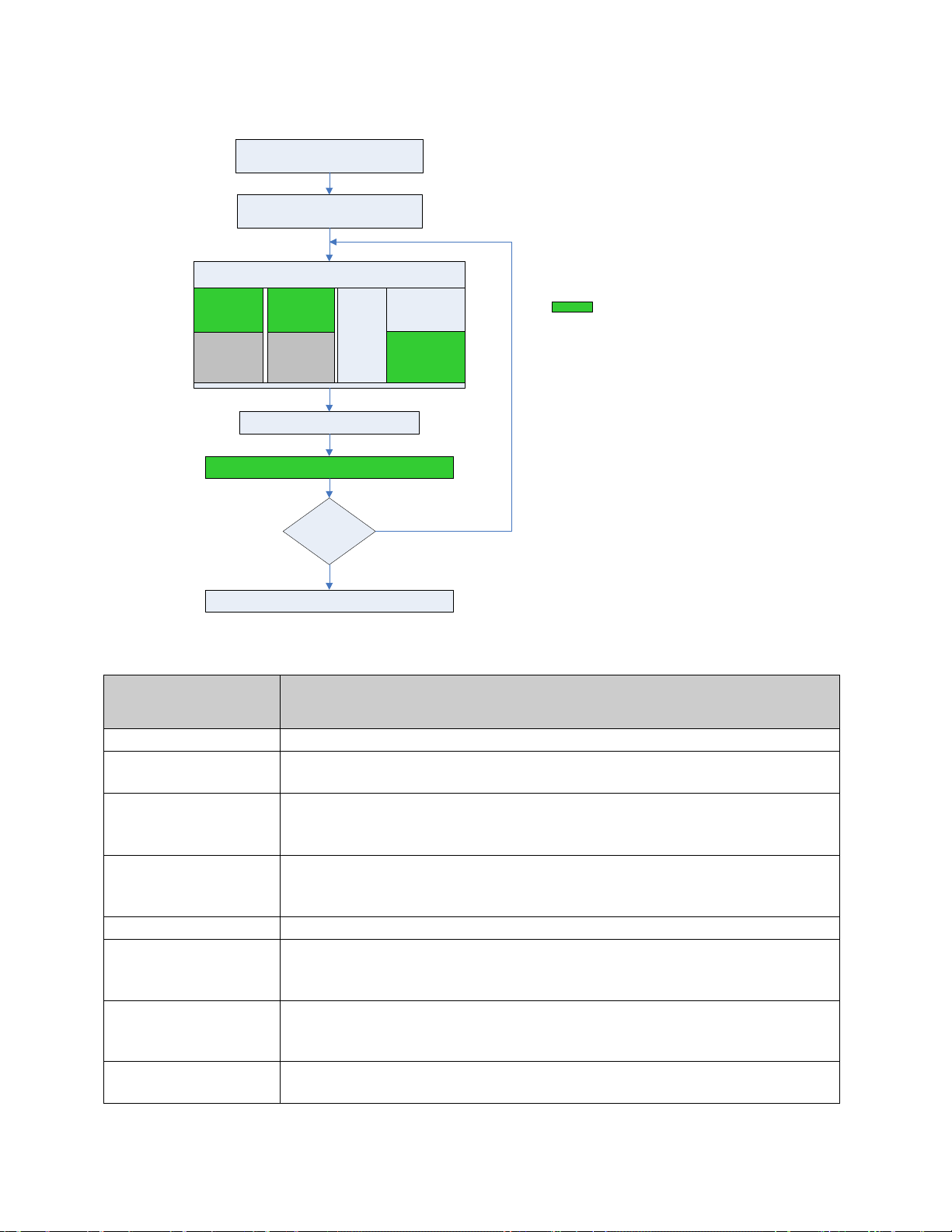
1.2 Cypress CapSense Documentation Ecosystem
Figure 1-1 and Table 1-1 summarize the Cypress CapSense documentation ecosystem. These resources allow
implementers to quickly access the information needed to successfully complete a CapSense product design.
Figure 1-1 shows the typical flow of a product design cycle with capacitive sensing; the information in this guide is
most pertinent to the topics highlighted in green. Table 1-1 includes links to the supporting documents for each of the
numbered tasks in Figure 1-1.
CY8C21x34/B CapSense® Design Guide Document No. 001-66271 Rev. *B 7
Page 8
2. CapSense device selection based
on needed functionality
3. Mechanical
Design
4. Schematic
capture and
PCB layout
1. Specify system requirements and
characteristics
5. PSoC
Designer
project
creation
Preproduction build (prototype)
6. Firmware
development
7. CapSense
configuration
and tuning
8. Test and evaluate system functionality and
CapSense performance
Design for CapSense
Performance
satisfactory
Production
Yes
No
= Topics covered in this document
Figure 1-1. Typical CapSense Product Design Flow
Numbered Design Task of
Figure 1-1
1 Getting Started with CapSense
2
3
4
5 PSoC Designer User Guides
6
7
8
Table 1-1. Cypress Documents Supporting Numbered Design Tasks of Figure 1-1
Supporting Cypress CapSense Documentation
Getting Started with CapSense
CY8C21x34/B CapSense Device Datasheets
Getting Started with CapSense
PSoC Family Specific CapSense
CapSense Application Notes
Getting Started with CapSense
PSoC Family Specific CapSense
CapSense Application Notes
CapSense Application Notes
CapSense Code Examples
PSoC Family Specific Technical Reference Manual (for CY8C21x34/B)
PSoC Family Specific CapSense Design Guide (this document)
PSoC Family Specific CapSense User Module Datasheets (CSD, CSDADC, and SmartSense)
PSoC Family Specific Technical Reference Manual (for CY8C21x34/B)
PSoC Family Specific CapSense Design Guide (this document)
CapSense Code Examples
Design Guide (this document)
Design Guide (this document)
8 Document No. 001-66271 Rev. *B CY8C21x34/B CapSense
®
Design Guide
Page 9

1.3 CY8C21x34/B CapSense Plus Family Features
Cypress’s CY8C21x34/B is a low-power, high-perfor ma nce, progr a mm able CapSense controller family that features:
1.3.1 Advanced Touch Sensing Features
Programmable capacitive sensing elements
Supports a combination of CapSense buttons, sliders, and proximity sensors with CSD and CSDADC
capacitive sensing technology
SmartSense™ Auto-tuning (CY8C21x34B)
Contains an integrated API to implement buttons and sliders
Supports up to 24 capacitive buttons and 4 sliders
Supports proximity sensing up to 5 cm (with on-board PCB trace)
Water-tolerant performance with shield electrode
1.3.2 Device Features
High-performance, low-power M8C Harvard-architec tur e pro ces sor
M8C processor speeds up to 24 MHz
Flexible on-chip memory
Up to 8 KB of flash and 512 B of SRAM
Emulated EEPROM supported
Precision, progra mma ble cloc king
Internal main oscillator (IMO): 24/48 MHz ± 2.5%
Internal low-speed oscillator (ILO) at 32 kHz for watchdog and sleep
Enhanced general-purpose input/output (GPIO) features
Up to 28 general-purpose I/Os (GPIOs) with programmable pin configuration
25-mA sink current on all GPIOs
Internal resistive pull-up, HI-Z, open-drain, and strong drive modes on all GPIOs
Peripheral features
Counter, timer, PWM, Pulse Width Discriminator (PWD), and hardware 7-segment drive
2
I
C communication with Master, Slave, and Multi-Master configurations
SPI, UART, IRDA, and one-wire communication protocols
Operating Conditions
Operating Voltage: 2.4 V to 5.25 V with operation down to 1.0 V by using on-chip switch mode pump
Temperature Range: –40
Packaging
16-pin SOIC (150-MIL) to 32-pin QFN (5 x 5 mm)
AEC qualified automotive grade parts – CY8C21334 and CY8C21534
o
C to +85 oC
CY8C21x34/B CapSense® Design Guide Document No. 001-66271 Rev. *B 9
Page 10

1.4 Document Conventions
Convention Usage
Courier New
Italics
[Bracketed, Bold]
File > Open
Bold
Times New Roman
Text in gray boxes Describes Cautions or unique functionality of the product.
Displays file locations, user entered text, and source code:
C:\ ...cd\icc\
Displays file names and reference documentation:
Read about the sourcefile.hex file in the PSoC Designer User Guide.
Displays keyboard commands in procedures:
[Enter] or [Ctrl] [C]
Represents menu paths:
File > Open > New Project
Displays commands, menu paths, and icon names in procedures:
Click the File icon and then click Open.
Displays an equation:
2 + 2 = 4
10 Document No. 001-66271 Rev. *B CY8C21x34/B CapSense
®
Design Guide
Page 11
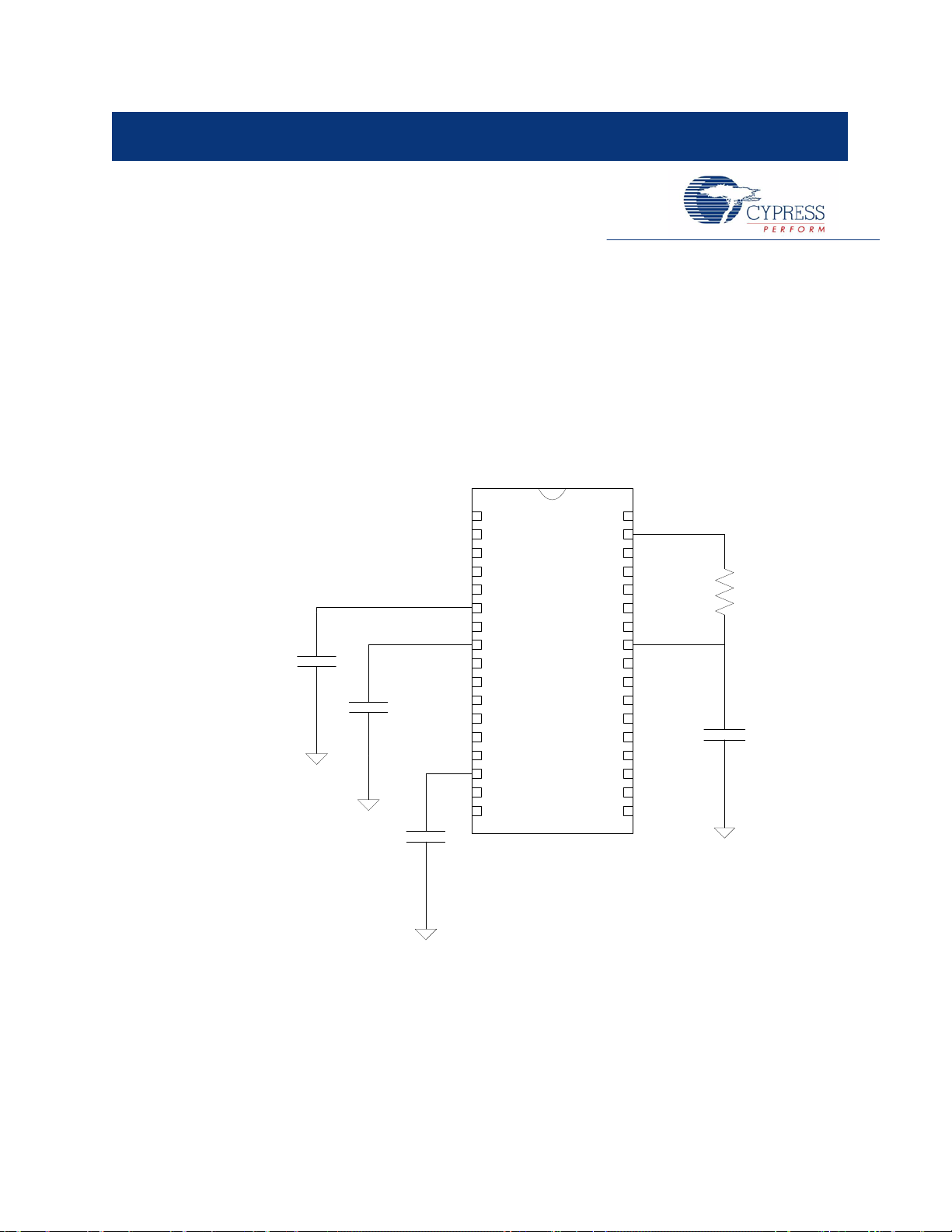
2. CapSense Technology
CY8C21x34/B Rb
Cmod
Cx,n
Cx,2
Cx,1
Sensor Equivalent
Capacitors
P1[1] or P1[5]
P0[1] or P0[3]
2.1 CapSense Fundamentals
CapSense is a touch-sensing technology that works by measuring the capacitance of each I/O pin on the CapSense
controller that has been designated as a sensor. As shown in Figure 2-1, the total capacitance on each of the sensor
pins can be modeled as equivalent lumped capacitors with values of C
Circuitry internal to the CY8C21x34/B device converts the magnitude of each C
post processing. The other components, namely Rb and C
circuitry.
Figure 2-1. CapSense Implementation in a CY8C21x34/B PSoC Device
, are used by the CapSense controller’s internal
MOD
through C
X,1
X
for a design with n sensors.
X,n
into a digital code that is stored for
As shown in Figure 2-2, each sensor I/O pin is connected to a sensor pad by traces, vias, or both as necessary. The
overlay is a nonconductive cover over the sensor pad that constitutes the product’s touch interface. When a f inger
comes into contact with the overlay, the conductivity and mass of the body effectively introduces a grounded
conductive plane parallel to the sensor pad. This is represented in Figure 2-2. This arrangement constitutes a pa r all e l
plate capacitor whose capacitance is given by Equation 1.
.
CY8C21x34/B CapSense® Design Guide Document No. 001-66271 Rev. *B 11
Page 12

D
A
C
r
F
εε
0
=
PX
CC =
FPX
CCC +=
Figure 2-2. Cross Section of Typical CapSense PCB with the Sensor Being Activated by a Finger
Equation 1
Where:
CF = The capacitance affected by a finger in contact with the overlay over a sensor
ε
= Free space permittivity
0
= Dielectric constant (relative permittivity) of overlay
ε
r
A = Area of finger and sensor pad overlap
D = Overlay thickness
In addition to the parallel plate capacitance, a finger in contact with the overlay causes electric field fringing between
itself and other conductors in the immediate vicinity. The effect of these fringing fields is typically minor compared to
that of the parallel plate capacitor and can usually be ignored.
Even without a finger touching the overlay, the sensor I/O pin has some parasitic capacitance (C
). CP results f rom
P
the combination of the CapSense controller internal parasitics and electric field coupling between the sensor pad,
traces, and vias, and other conductors in the system such as ground plane, other traces, any metal in the product’s
chassis or enclosure, and so on. The CapSense controller measures the total capacitance (C
) connected to a
X
sensor pin.
When a finger is not touching a sensor:
Equation 2
When a finger is touching the sensor:
Equation 3
In general CP is an order of magnitude greater than CF. CP usually ranges from 6 pF to 15 pF, but in extreme cases
can be as high as 50 pF. CF usually ranges from 0.1 pF to 0.4 pF. The magnitude of C
is of critical importance when
P
tuning a CapSense system and will be discussed in CapSense Performance Tuning with User Modules.
12 Document No. 001-66271 Rev. *B CY8C21x34/B CapSense
®
Design Guide
Page 13

Cx
Vdd
i
sensor
Sigma-Delta
Converter
Precharge
Clock
Cmod
Rb
High-Z
input
Sw1
Sw2
CY8C21x34/B
Gnd
i
bleed
= External Connection
AMUX Bus
Vref
Rbus
R
inline
2.2 CapSense Methods in CY8C21x34/B
CY8C21x34/B devices support several CapSense methods for converting sensor capacitance (CX) into a digi t al co de.
These are CapSense Sigma Delta (CSD), CSD with ADC (CSDADC), and SmartSense. These methods are
implemented in the form of PSoC Designer User Modules and are described in Section 3 of this design guide.
2.2.1 CapSense with Sigma Delta Modulator (CSD)
The CapSense Sigma-Delta (CSD) method in CY8C21x34/B devices incorporates CX into a switched-capacitor circuit
as shown in Figure 2-3. The sensor (C
underlapped switches Sw1 and Sw2, respectively. Sw1 and Sw2 are driven by a Precharge clock to generate a
current (I
) into the AMUX bus. The magnitude of I
SENSOR
Sigma-Delta converter samples AMUX bus voltage and generates a modulating bit stream that controls the constant
current source (I
sensor bleeds off the charge I
), which charges AMUX such that the average AMUX bus voltage is maintained at V
DAC
SENSOR
low-pass filter that attenuates Precharge switching transients at the Sigma-Delta converter input.
) is alternately connected to VDD and the Analog MUX (AMUX) bus by the
X
is directly proportional to the magnitude of CX. The
SENSOR
from the modulating capacitor (C
MOD
). C
in combination with Rbus forms a
MOD
Figure 2-3. CSD Block Diagram
REF
. The
In maintaining the average AMUX voltage at a steady state value (V
average bleed current (I
BLEED
) to I
by controlling the bit stream duty cycle. The Sigma-Delta converter stores
SENSOR
), the Sigma-Delta converter matches the
REF
the bit stream over the duration of a sensor scan and the accumulated result is a digital output value, known as raw
counts, that is directly proportional to C
state. Figure 2-4 plots the CSD raw counts from a number of consecutive scans during which the sensor is touched
and then released by a finger. As explained in CapSense Fundamentals, the fing er touch caus es C
which in turn causes raw counts to increase proportionally. By comparing the shift in steady state raw count level
C
F,
. This raw count is interpreted by high-level algorithms to resolve sensor
x
to increase by
x
to a predetermined threshold, the high-level algorithms can determine whether the sensor is in an On (Touch) or Off
(No Touch) state.
CY8C21x34/B CapSense® Design Guide Document No. 001-66271 Rev. *B 13
Page 14

Figure 2-4. CSD Raw Counts during a Finger Touch
2.2.2 CSD with ADC Functionality (CSDADC)
The CSDADC CapSense method functions in an identical manner as CSD except that it is augmented with the ADC
functionality in addition to capacitance measurement.
2.2.2.1 ADC Features
Absolute and ratiometric ADC input modes with run-time mode switching, which allows you to easily scan
different sensor types
Single-slope ADC for absolute voltage input mode
Built-in calibration mechanism for the single-slope ADC
Integrating incremental ADC for ratiometric input mode
2.2.3 SmartSense™ Auto-tuning
Tuning the touch-sensing user interface is a critical step in ensuring proper system operation and a pleasant user
experience. The typical design flow entails tuning the sensor interface in the initial design phase, during system
integration, and finally production fine-tuning before the production ramp. Tuning is an iterative process and can be
time consuming. SmartSense Auto-tuning was developed to simplify the user interface development cycle. It is easy
to use and significantly reduces the design cycle time by eliminating the tuning process throughout the entire product
development cycle, from prototype to mass production. SmartSense tunes each CapSense sensor automatically at
power up and then monitors and maintains optimum sensor performance during run time. This technology adapts for
manufacturing variation in PCBs, overlays, and noise generators such as LCD inverters, AC line noise, and switchmode power supplies, and automatically tunes them out. SmartSense Auto-tuning requires between 2.1 KB -3.7 KB
of flash depending on configuration and 29B of RAM per sensor.
2.2.3.1 Process Variation
The SmartSense User Module (UM) for the CY8C21x34B is designed to work with sensor parasitic capacitance in the
range of 5 pF to 45 pF (typical sensor CP values are in the range of 10 pF to 20 pF). The sensitivity parameter for
each sensor is set automatically, based on the characteristics of that particular sensor. This improves the yield in
mass production, as consistent response is maintained from every sensor regardless of C
within the specified range of 5 to 41 pF. Parasitic capacitance of the individual sensors can vary due to PCB layout,
PCB manufacturing process variation, or with vendor-to-vendor PCB variation within a multisourced supply chain.
The sensitivity of a sensor depends on its parasitic capacitance; higher C
result in decreased finger touch signal amplitude. In some cases, the change in C
resulting in less than optimum sensor performance (either too sensitive or not sensitive enough) or, wor st case, a
nonoperational sensor. In either situation, you must retune the system, and in some cases requalify the UI
subsystem. SmartSense Auto-tuning solves these issues.
values decrease the sensor sensitivity and
P
variation between sensors
P
value detunes the system,
P
14 Document No. 001-66271 Rev. *B CY8C21x34/B CapSense
®
Design Guide
Page 15
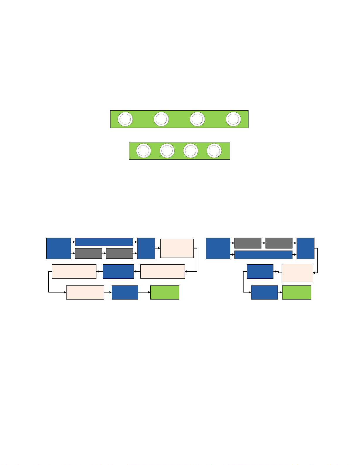
Feasibility
Study
Schematics
Design
PCB Layout
Design
Mechanical Design
Review
System
Integration
Re-tuning for any
changes
Tuning process
Production Fine
Tuning
Design
Validation
Production
Typical capacitive user interface Design Cycle
Firmware
Development
Feasibility
Study
Schematics
Design
PCB Layout
Design
Mechanical Design
Review
System
Integration
Design
Validation
Production
SmartSense based capacitive user interface Design Cycle
Firmware
Development
SmartSense Auto-tuning makes platform designs possible. Imagine the capacitive touch sensing multimedia keys in a
laptop computer; the spacing between the buttons depends on the size of the laptop and keyboard layout. In this
example, the wide-screen machine has larger spaces between the buttons than a standard-screen model. More
space between buttons means increased trace length between the sensor and the CapSense controller, which leads
to higher parasitic capacitance of the sensor. This means that the parasitic capacitance of the CapSense buttons can
be different in different models of the same platform design. Though the functionality of these buttons is the same for
all of the laptop models, the sensors must be tuned for each model. SmartSense enables you to do platform designs
using the recommended best practices shown in the PCB Layout in Getting Started with CapSense, knowing the
tuning will be done efficiently and automatically.
Figure 2-5. Design of Laptop Multimedia Keys for a 21-inchModel
Figure 2-6. Design of Laptop Multimedia Keys for a 15-inchModel with Identical Functionality and Button Size
2.2.3.2 Reduced Design Cycle Time
Usually the most time-consuming task for a capacitive sensor interface design is firmware development and sensor
tuning. With a typical touch-sensing controller, the sensor must be retuned when the same design is ported to
different models or when there are changes in the mechanical dimensions of the PCB or the sensor PCB layout. A
design with SmartSense solves these challenges because it needs less firmware development effort, no tuning, and
no retuning. This makes a typical design cycle much faster. Figure 2-7 compares the design cycles of a t ypi c al t ouc h sensing controller and a SmartSense-based design.
Figure 2-7. Typical Capacitive Inter fa ce Design Cycle Comparison
CY8C21x34/B CapSense® Design Guide Document No. 001-66271 Rev. *B 15
Page 16

3. CapSense Design Tools
3.1 Overview of CapSense Design Tools
Cypress offers a full line of hardware and software tools for developing your CapSense capacitive touch-sense
application. A basic development system for the CY8C21x34/B family includes the components discussed in this
chapter. See Resources for ordering information.
3.1.1 PSoC Designer™ and User Modules
Cypress’s exclusive integrated design environment, PSoC Designer, allows you to configure analog and digital
blocks, develop firmware, tune, and debug your design. Applications are developed in a drag-and-drop design
environment using a library of user modules. User modules are configured either through the Device Editor GUI or by
writing into specific registers with firmware. PSoC Designer comes with a built-in C compiler and an embedded
programmer. A pro compiler is available for complex designs.
CSD, CSDADC, and SmartSense User Modules implement capacitive touch sensors using switched-capacitor
circuitry, an analog multiplexer, a comparator, digital counting functions, and high-level software routines (APIs). User
modules for other analog and digital peripherals are available to implement additional functionality such as I
TX8, Timers, and PWMs.
Figure 3-1. PSoC Designer Device Editor
2
C, SPI,
3.1.1.1 Gett ing Started with CapSense User Modules
To create a new CY8C21x34/B project in PSoC Designer:
1. Create a new CY8C21x34/B PSoC Designer proje ct.
2. Select and place any user modules requiring dedicated pins (such as I
3. Select and place the CSD, CSDADC, or SmartSense User Module.
4. Right-click the user module to access the User Module wizard.
5. Set button sensor count, slider configuration, pin assignments, and associations.
6. Set pins and global user mod u le parame ter s .
16 Document No. 001-66271 Rev. *B CY8C21x34/B CapSense
2
C or LCD) and assign ports and pins.
®
Design Guide
Page 17
DC Supply
Jack
5-V Voltage
Regulator IC
SPI / I2C
Expansion Header
ISSP Header
LEDs D1 and D2
Adjustable
Voltage
Regulator IC
CapSense
Controller
CY8C21001
Jumper for
XRES Selection
CapSense Module
Connector
ICE Cube
Connector
Jumper to Select
Power Option
9-V Battery
Terminal
7. Generate the application and switch to Application Editor.
8. Adapt sample code from U ser Module Datasheet: (CY8C21x34) to implement buttons or sliders.
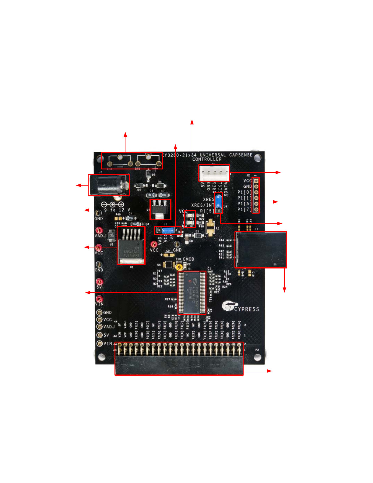
3.1.2 Universal CapSense Controller Kit
The Universal CY3280-BK1 CapSense Controller Kit features predefined control circuitry and plug-in hardware to
make prototyping and debugging easy. Programming and I2C-to-USB Bridge hardware are included for tuning and
data acquisition.
Figure 3-2. CY3280-21x34 CapSense Controller Kit
CY8C21x34/B CapSense® Design Guide Document No. 001-66271 Rev. *B 17
Page 18
3.1.3 Universal CapSense Controller Module Board
Cypress’s module boards feature a variety of sensors, LEDs, and interfaces to meet your application’s needs.
CY3280-BSM Simple Butto n Module
CY3280-BMM Matrix Button Module
CY3280-SLM Linear Slider Module
CY3280-SRM Radial Slider Module
CY3280-BBM Universal CapSense Prototyping Module
3.1.4 CapSense Data Viewing Tools
Many times during the CapSens e design process, you will want to monitor CapSense data (raw counts, baseline,
difference counts, and so on) for tuning and debugging purposes. There are two CapSense Data Viewing Tools,
MultiChart, and Bridge Control Panel. These tools are explained in more detail in the application note
AN2397 – CapSense Data Viewing Tools.
3.2 User Module Overview
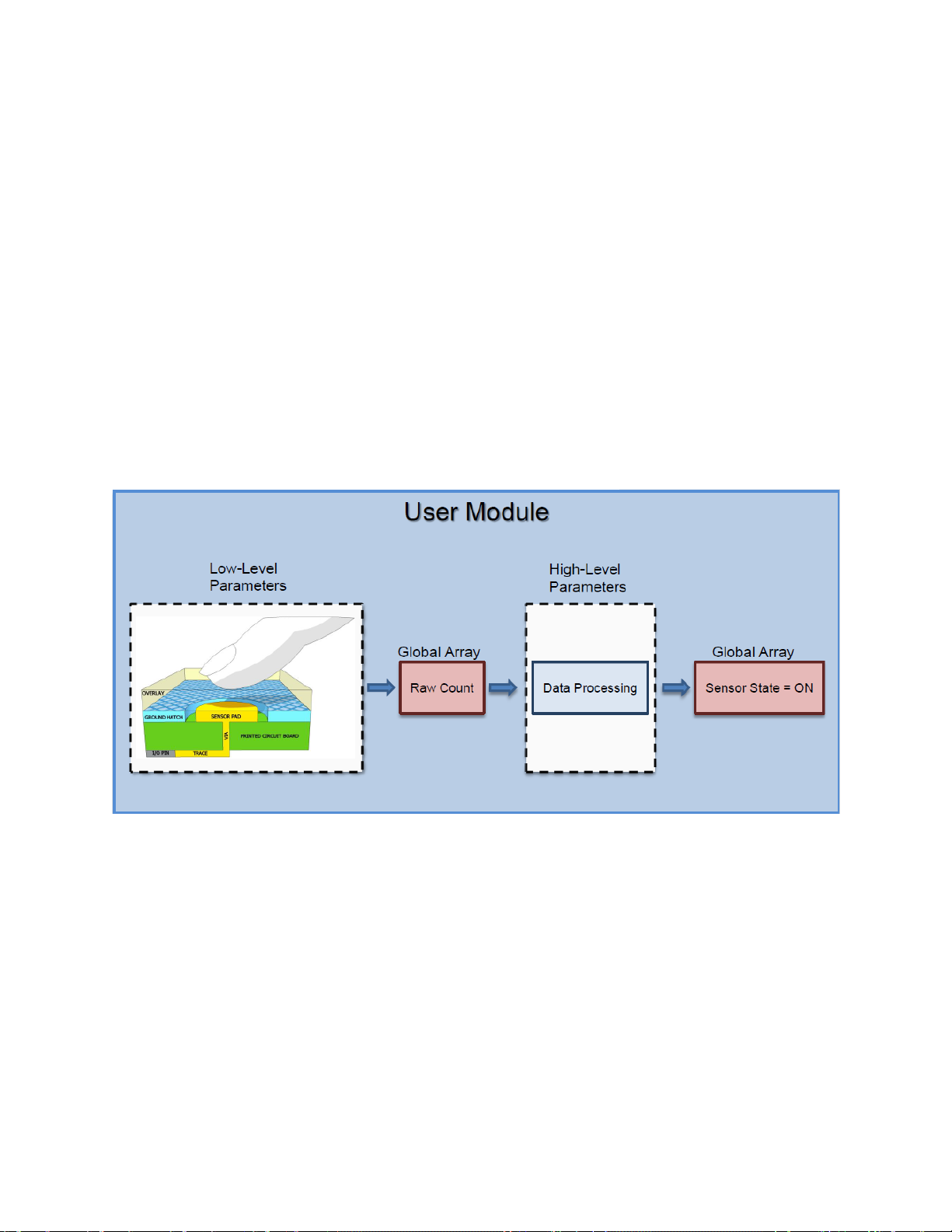
Figure 3-3. User Module Block Diagram
User modules contain an entire CapSense system from physical sensing to data processing. The behavior of the user
module is defined using several parameters. These parameters affect different parts of the sensing system and can
be separated into low-level and high-level parameters that communicate with one another using global arrays.
Low-level parameters, such as the speed and resolutions for scanning sensors, define the behavior of the sensing
method at the physical layer, and relate to the conversion from capacitance to raw count. Low-level parameters are
unique to each type of sensing method and are described in CSDADC User Module Configurations, CSDADC Use r
Module Parameters, and SmartSense User Module Parameters.
High-level parameters, such as debounce counts and noise thresholds, define how the raw counts are processed to
produce information such as the sensor ON/OFF state and the estimated finger position on a slider. These
parameters are the same for all sensing methods and are described in CSD User Module High-Level Parameters.
3.3 CapSens e Us e r Module Global Arrays
Before learning CapSense User Module parameters, you must be familiar with certain global arrays used by the
CapSense system. These arrays should not be altered manually, but may be inspected for debugging purposes.
18 Document No. 001-66271 Rev. *B CY8C21x34/B CapSense
®
Design Guide
Page 19

Difference Count
(Signal)
Raw Count
Figure 3-4. Raw Count, Baseline, Difference Count, and Sensor State
3.3.1 Raw Count
The hardware circuit in the CapSense controller measures the sensor capacitance. It stores the result in a digital form
called raw count upon calling the user module API UMname_ScanSensor(), where UMname can be CSD, CSDADC,
or SmartSense.
The raw count of a sensor is proportional to its sensor capacitance. Raw count increases as the sensor capacitance
value increases.
The raw count values of sensors are stored in the UMname_waSnsResult[] integer array. This array is defined in the
header file UMname.h.
3.3.2 Baseline
Gradual environmental changes such as temperature and humidity affect the sensor raw count, which results in
variations in the counts.
The user module uses a complex baselining algorithm is to compensate for these variations. The algorithm uses
baseline variables to accomplish this. The baseline variables keep track of any gradual variations in raw count values.
Essentially, the baseline variables hold the output of a digital low pass filter to which input raw count values are fed.
The baselining algorithm is executed by the user module API UMname_UpdateSensorBaseline, where UMname can
be CSD, CSDADC, or SmartSense.
The baseline values of sensors are stored in UMname_waSnsBaseline[] integer array. This array is defined in the
header file UMname.h.
3.3.3 Difference Count (Signal)
The Difference Count, which is also known as the signal of a sensor, is defined as the difference in counts between a
sensor’s raw count and baseline values. When the sensor is inactive, the Difference Count is zero. Activating sensors
(by touching) results in a positive Difference Count value.
The Difference Count values of sensors are stored in the UMname_waSnsDiff[] integer array, where UMname can be
CSD, SmartSense, or CSA_EMC. This array is defined in the header file UMname.h.
Difference count variables are updated by the user module API UMname_UpdateSensorBaseline()..
3.3.4 Sensor State
Sensor state represents the active/inactive status of the physical sensors. The state of the s ensor changes from 0 to
1 upon finger touch and returns to 0 upon finger release.
Sensor states are stored in a byte array named UMname_baSnsOnMask[]array, where UMname can be CSD,
CSDADC, or SmartSense. Each array element stores the sensor state of eight consecutive sensors.
CY8C21x34/B CapSense® Design Guide Document No. 001-66271 Rev. *B 19
Page 20
High-Level
Low-Level
Sensor states are updated by the user module API UMname_bIsAnySensorActive()
3.4 CSD User Module Configurations
The CSD User Module has two selectable clock configurations. These configurations use different signal sources for
the switched-capacitor circuit on the front end of the CSD, as shown in Fi gure 2-3 on page 13.
You should select the clock configuration when you first place the CSD Us er Module in your PSoC Designer project.
You can change this selection later by right-clicking the CSD User Module and selecting User Module Selection
Options.
3.4.1 CSD without Clock Prescaler
In this configuration, a 16-bit pseudo-random sequence (PRS) is used as the signal source for the switched-capacitor
circuit on the front end of the CSD. System Clock (IMO) is the clock source for the PRS. The PRS spreads the clock’s
frequency spectrum and provi des good noise immunity. This configuration requires three digital blocks.
3.4.2 CSD with Clock Prescaler
In this configuration, an 8-bit PRS is used as the signal source for the switched capacitor circuit on the front end of
the CSD. IMO is divided by an adjustable prescaler divider and is used as the clock source for the PRS. The PRS
spreads the clock’s frequency spectrum to provide noise immunity. Note that the 16-bit PRS used in the CSD without
the Clock Prescaler configuration provides better noise immunity. This configuration requires three digital blocks.
Because it needs a lower switching frequency, use this configuration when operating in an environment with high C
The relationship between CP and switching frequency is discussed in Select Prescaler.
P.
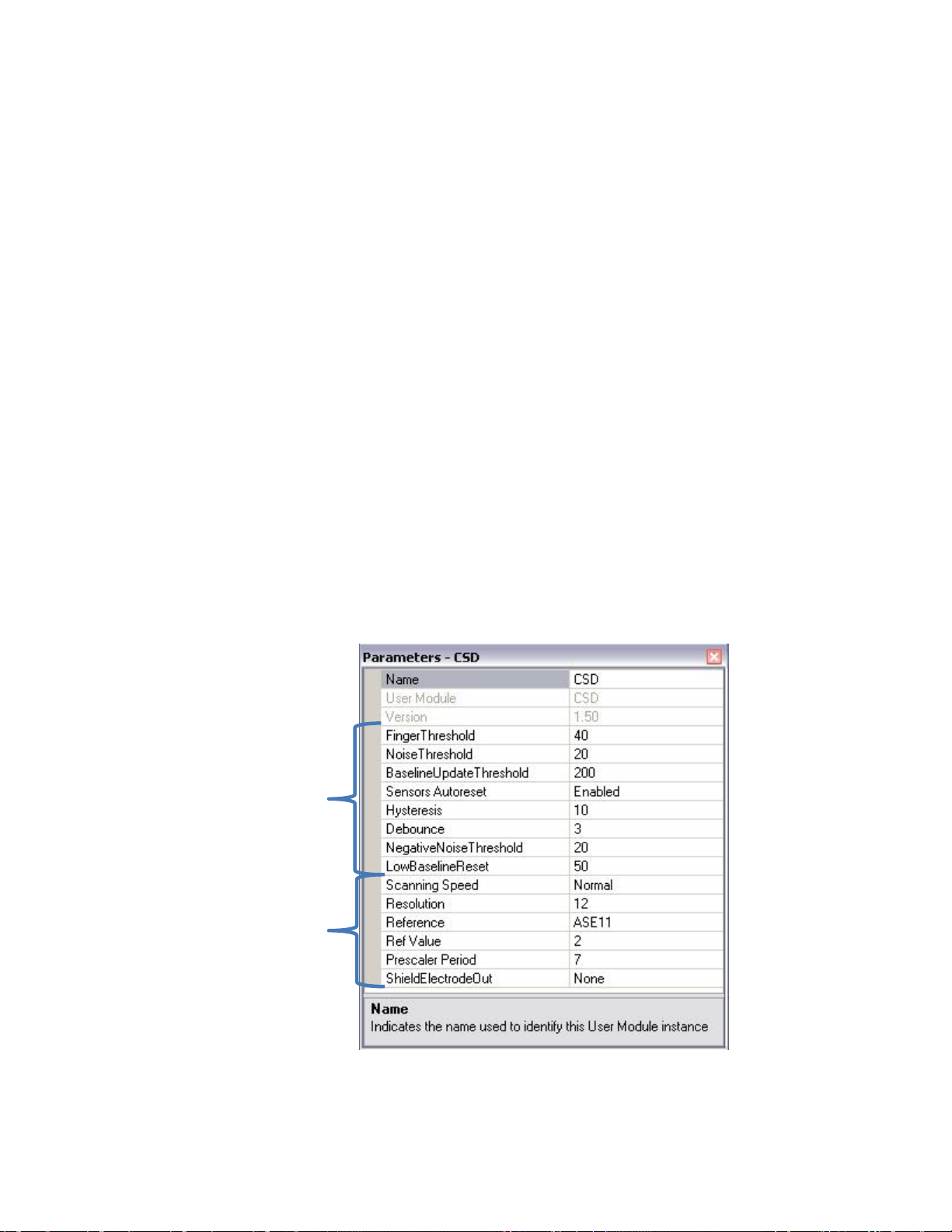
3.5 CSD User Module Parameters
The CSD User Module parameters are classified into high-level and low-level parameters. See Figure 3-5 for a list of
CSD user module parameters and how they are classified.
Figure 3-5. PSoC Designer - CSD Parameters Window
20 Document No. 001-66271 Rev. *B CY8C21x34/B CapSense
®
Design Guide
Page 21

3.6 CSD User Module High-Level Parameters
3.6.1 Finger Threshold
The Finger Threshold parameter is used by the user module to judge the active/inactive state of a sensor. If the
Difference Count value of a sensor is greater than the Finger Threshold value, the sensor is judged as active. This
definition assumes that Hysteresis is set to zero and Debounce is set to 1.
Possible values are 5 to 255.
3.6.2 Noise Threshold
The user module uses the Noise Threshold value to interpret the upper limit of noise counts in the raw count. For
individual sensors, the baselining update algorithm is paused when the raw count is greater than the baseline and the
difference between them is greater than this threshold.
For slider sensors, the centroid calculation is paused when the difference count is greater than the Noise Threshold
value.
Possible values are 3 to 255. For proper user module operation, the Noise Threshold value should never be set
higher than Finger Threshold value minus the Hysteresis setting.
3.6.3 Baseline Update T hr eshold
When the raw count value is above the current baseline and the difference count is below the noise Threshold, the
difference between the current baseline and the raw count is accumulated into a "bucket." When the bucket fills
completely, the baseline increments and the bucket is emptied. The Baseline Update Threshold parameter sets the
threshold that the bucket must reach for the baseline to increment.
Possible values are 0 to 255.
3.6.4 Sensors Autor eset
The Sensors Autoreset parameter determines whether the baseline is updated at all times, or only when the
difference counts are less than the Noise Threshold value.
When Sensors Autoreset is enabled, the baseline is updated constantly. This limits the maximum time duration of the
sensor but prevents the sensors from permanently turning on when the raw count accidentally rises without anything
touching the sensor. This sudden rise can be caused by a large voltage fluctuation in the power supply, a high-energy
RF noise source, or a very quick temperature change.
When Sensors Autoreset is disabled, the baseline is updated only when the difference counts are less than the Noise
Threshold parameter.
Possible values are Enabled and Disabled.
3.6.5 Hysteresis
The Hysteresis setting prevents the sensor ON state from chattering because to system noise. The function of
Hysteresis is given in Equation 4. The equation assumes that Debounce is set to 1.
CY8C21x34/B CapSense® Design Guide Document No. 001-66271 Rev. *B 21
Page 22

Figure 3-6. Sensor State Versus Difference Count with Hysteresis Set to Zero
Equation 4
3.6.6 Debounce
The Debounce parameter prevents spikes in raw counts from changing the sensor state from OFF to ON. For the
sensor state to transition from OFF to ON, the Difference Count value must remain greater than the Finger Threshold
value plus the hysteresis level for the number of samples specified.
Possible values are 1 to 255. A setting of 1 provides no debouncing.
3.6.7 Negative Noise Threshold
The Negative Noise Threshold parameter acts as a negative difference count threshold. If the raw count is less than
the baseline minus the negative noise threshold for the number of samples specified by the Low Baseline Reset
parameter, the baseline is set to the new raw count value.
Possible values are 0 to 255.
3.6.8 Low Baseline Reset
The Low Baseline Reset parameter works in conjunction with the Negative Noise Threshold parameter. It counts the
number of abnormally low samples required to reset the baseline. It is used to correct the finger-on-at-startup
condition.
Possible values are 0 to 255.
3.6.9 High Level Parameter Recommendations
The following recommendations are a starting place for selecting the optimal parameter settings.
Finger Threshold: Set to 75 percent of Difference Counts with sensor ON
Noise Threshold: Set to 40 percent of Difference Counts with sensor OFF
Baseline Update Threshold: Set to two times Noise Threshold
Sensors Autoreset: Based on design requirements
Hysteresis: Set to 15 percent of Difference Counts with sensor ON
Debounce: Based on design requirements
22 Document No. 001-66271 Rev. *B CY8C21x34/B CapSense
®
Design Guide
Page 23

Scanning Speed (µs)
Ultra Fast
Fast
Normal
Slow
Scanning Speed (µs)
Ultra Fast
Fast
Normal
Slow
Negative Noise Thresh old: Set equal to Noise Threshold
Low Baseline Reset: Set to 10
3.7 CSD User Module Low-Level Parameters
The CSD User Module has several low-level parameters in addition to the high-level parameters. These parameters
are specific to the CSD sensing method and determine how raw count data is acquired from the sensor.
3.7.1 Scanning Speed
This parameter sets the sensor scanning speed. Although a faster scanning speed provides a good response time,
slower scanning speeds give the following advantages:
Improved SNR
Better immunity to power supply and temperature changes
Less demand for system interrupt latency; you can handle longer interrupts
See Table 3-1 and Table 3-2 for scanning speed and resolution performance.
Possible values are Ultra Fast, Fast, Normal, and Slow.
3.7.2 Resolution
This parameter determines the scanning resolution in bits. The maximum raw count for scanning resolution of N bits
N-1
. Increasing the resolution improves sensitivity and SNR, but reduces scan time. See Table 3-1 and Table 3-2
is 2
for scanning speed and resolution performance. Possible values are 9 to 16 bits.
Table 3-1. Scanning Speed and Resolution for 24-MHz IMO Operation, without Clock Prescaler (PRS16
Configuration)
Resolution
(bits)
9 75 110 170 300
10 110 170 300 510
11 170 300 510 1010
12 300 510 1010 2030
13 510 1010 2030 4060
14 850 1690 3380 6760
15 1520 3040 6080 12200
16 2880 5720 11500 23200
Table 3-2. Scanning Speed and Resolution for 24- MHz IMO Operation, with Prescaler (PRS8 Configuration)
Resolution
(bits)
9 60 85 150 255
10 85 150 255 510
11 150 255 510 1020
12 255 510 1020 2040
13 510 1020 2010 4080
14 845 1700 3380 6760
15 1530 3060 6120 12100
16 2880 5800 11500 23000
CY8C21x34/B CapSense® Design Guide Document No. 001-66271 Rev. *B 23
Page 24

3.7.3 Reference
A voltage reference to the input of the comparator is required for the proper operation of CSD.
Possible values are:
VBG: Internal voltage reference of 1.3 V derived from a fixed bandgap reference.
ASE11: Internal variable voltage reference derived from a PWM.
AnalogColumn_InputSelect_1: External voltage reference such as a resistor divider network or externally filtered
PWM/PRSPWM signal. This reference can be connected to a CapSense controller pin and used as the
comparator reference source.
3.7.4 Ref Value
The effect of this parameter depends on the Reference parameter selection. This value has no effect when the
reference comes from the VBG or from AnalogColumn_InputSelect_1. When the reference comes from ASE11, this
parameter sets the reference value.
Possible values are: 0 (minimum ¼V
) to 8 (maximum ¾ VDD).
DD
3.7.5 Prescaler Period
The sensor capacitance is switched continuously between two potentials while scanning. This parameter sets the
prescaler period register and determines the precharge switch output frequency. This parameter is available only for
CSD with the clock prescaler configuration.
Possible values are1 to 255.
3.7.6 Shield Electrod e O ut
Shield Electrode Out should be enabled for applications requiring water-tolerant performance. The shield electrode
signal source can be selected from one of the free digital row buses (Row_0_Output_1 to Row_0_Output_3). Each
row output can be routed to one of three pins. Set the Row LUT Function to A.
Possible values are Enabled and Disabled.
3.8 CSDADC User Module Configurations
The CSDADC combines capacitance sensing with ADC functionality. It saves code space by reusing modules
common to both the CSD and ADC. You should use the CSDADC when your design requires both capacitance
sensing and ADC functionality. Applications that need one or the other should use the CSD User Module or the ADC8
or ADC10 User Modules.
There are four selectable clock configurations for the CSDADC User Module: PRS16, PWM8, PRS8, and VC2. These
configurations use different signal sources for the switched capacitor circuit on the front end of the CSD
You should select the clock configuration when you first place the CSDADC User Module into your PSoC Designer
project. You can change this selection later by right-clicking the CSD ADC User Module and selecting User Module
Selection Options.
3.8.1 CSDADC with PRS16 Clock Source
In this configuration, a 16-bit pseudo-random sequence (PRS) is used as the signal source for the switched-capacitor
circuit on the front end of the CSD. System Clock (IMO) is the clock source for the PRS. The PRS spreads the clock’s
frequency spectrum and provi des good noise immunity. This configuration requires three digital blocks.
3.8.2 CSDADC with PRS8 Clock Source
In this configuration, an 8-bit PRS is used as the signal source for the switc hed-capacitor circuit on the front end of
the CSD. System Clock (IMO) is the clock source for the PRS. The PRS spreads the clock’s frequency spectrum to
give noise immunity. Note that the 16-bit PRS used in the CSD without the Clock Prescaler configuration provides
better noise immunity. This configuration requires three digital blocks.
24 Document No. 001-66271 Rev. *B CY8C21x34/B CapSense
®
Design Guide
Page 25

Because it needs a lower switching frequency, you should use configuration when operating in an environment with
high C
User Modules.
, The relationship between CP and switching frequency is discussed in CapSense Performance Tuning with
P
3.8.3 CSDADC with PWM8 Clock Source
In this configuration, IMO is divided by an adjustable prescaler divider and used for the switched capacitor circuit on
the front end of the CSD. This configuration is more sensitive to noise at the frequency of operation and its
harmonics. This configuration requires two digital blocks.
This configuration is suitable for sensing through high-resistance materials (such as ITO) or when you want low
operation frequency because of emission problems.
3.8.4 CSDADC with VC2 Clock Source
In this configuration, the system clock is divided using an adjustable divider, VC2, and used for the switchedcapacitor circuit on the front end of the CSD. This configuration is more sensitive to noise signals at the frequency of
operation and its harmonics. This configuration requires one digital block.
This configuration is suitable for sensing through high-resistance materials (such as ITO) or when you want low
operation frequency because of emission problems.
3.9 CSDADC User Module Parameters
Figure 3-7. PSoC Designer - C SDAD C Parameters Windows
3.10 Low-Level Parameters
3.10.1 Scanning Speed
This parameter sets sensor scanning speed. Although faster scanning speed provides good response time, slower
scanning speeds provide the following advantages:
Improved SNR
Better immunity to power supply and temperature changes
Less demand for system interrupt latency; you can handle longer interrupts
See Table 3-1 and Table 3-2 for scanning speed and resolution performance. Possible values are Ultra Fast, Fast,
Normal, and Slow.
3.10.2 Resolution
This parameter determines the scanning resolution in bits. The maximum raw count for scanning resolution of N bits
N-1
is 2
. Increasing the resolution improves sensitivity and SNR, but reduces scan time. See Table 3-1 and Table 3-2
for scanning speed and resolution performance.
Possible values are 9 to 16 bits.
CY8C21x34/B CapSense® Design Guide Document No. 001-66271 Rev. *B 25
Page 26

3.10.3 Reference
A voltage reference to the input of the comparator is required for the proper operation of CSD.
Possible values are:
VBG: Internal voltage reference of 1.3 V derived from a fixed band-gap reference.
ASE11: Internal variable voltage reference derived from a PWM.
AnalogColumn_InputSelect_1: External voltage reference such as a resistor divider network or externally filtered
PWM/PRSPWM signal. This reference can be connected to a CapSense controller pin and used as the
comparator reference source.
3.10.4 Ref Value
The effect of Ref Value depends on the Reference parameter. When Reference is set to ASE11, Ref Value sets the
reference value.
Possible values are 0 (minimum ¼ VDD) to 8 (maximum ¾ VDD).
Increasing Ref Value decreases sensitivity, but increases the influence on the shield electrode. If the design has
sensors with noticeable capacitance differences (sensor pads of different sizes), you can use an API function to
balance raw counts by setting a higher Ref Value for the sensors with larger capacitance.
Ref Value has no effect when Reference is set to VBG or AnalogColumn_InputSelect_1. Ref Value is not available in
CSDADC with the VC2 clock source configuration.
3.10.5 Prescaler Period
Prescaler Period determines the precharge switch output frequency.
Possible values are 1 to 255. The recommended values are 2
15, 31, 63, 127, or 255). Other values can result in more noise, especially at low resolution and high scan speed.
Prescaler Period is available only for configurations with prescaler.
n – 1
to obtain the maximum signal-to-noise rati o (1 , 3, 7,
3.10.6 Shield E lec tr od e Out
The shield electrode signal source can be selected from one of the free digital row buses (Row_0_Output_1 to
Row_0_Output_3). Each row output can be routed to one of three pins. Set the Row LUT Function to A.
Possible values are Enabled and Disabled.
This parameter is available only in CSDADC with the PRS8/PRS16 clock source configurations. In CSDADC with the
PWM8 clock source configuration, the shield electrode signal is permanently connected to Row_0_Output_0.
3.10.7 ADC Enabled
When this parameter is set to Enabled, the ADC routines are included in the compliable code and can be called from
user code. When this parameter is set to Disabled, the ADC routines are not included. Setting this parameter to
Disabled can be useful in saving the flash memory if the ADC is no longer required by your design. When this
parameter is set to Disabled, the CSDADC User Module behaves the same as the CSD User Module.
26 Document No. 001-66271 Rev. *B CY8C21x34/B CapSense
®
Design Guide
Page 27
High-Level
Low-Level
Low-Level
Low-Level
High-Level
3.11 SmartSense User Module Parameters
Figure 3-8. PSoC Designer SmartSense Parameters
3.12 Low-Level Parameters
3.12.1 Shield E lec tr od e Out
A shield electrode is used to reduce parasitic capacitance. The shield electrode signal can be routed to one of the
free digital row buses (Row_0_Output_1 – Row_0_Output_3). Each row output can then be routed to one of the
allowed pins. Set the Row LUT Function to A.
3.12.2 Modulator Capacitor Pin
This parameter sets the pin to connect the external modulator capacitor (C
P0[3].
3.12.3 Feedback Resistor Pin
This parameter sets the pin to connect the external feedback resistor (Rb). Choose from the available pins: P1[1],
P1[5], P3[1]. Some pins are not available on some device packages. Use pins P1[5] or P3[1] to avoid programming
problems.
3.12.4 Threshold Setting Mode
Use this parameter to select between Automatic and Manual threshold settings.
3.12.5 Sensitivity Level
This parameter is used to increase and decrease the sensitivity of a sensor. Possible values are 0.1 pF (highest
sensitivity), 0.2 pF, and 0.4 pF (lowest sensitivity). Use a higher sensitivity setting for thicker overlay on capacitive
sensors.
). Choose from the available pins P0[1],
MOD
CY8C21x34/B CapSense® Design Guide Document No. 001-66271 Rev. *B 27
Page 28

3.12.6 Finger Threshold
This parameter is applicable only when threshold setting mode is set to Manual mode. It is recommended that you set
this value to 80 percent of the sensor signal stored in the SmartSense_baSnSSignal[] array. This array can be easily
monitored using I
2
C or UART communication protocols.
28 Document No. 001-66271 Rev. *B CY8C21x34/B CapSense
®
Design Guide
Page 29
4. CapSense Performance Tuning with User Modules
Optimal user module parameter settings depend on board layout, button dimensions, overlay material, and
application requirements. These factors are discussed in Design Considerat ions. Tuning is the process of identifying
the optimal parameter settings for robust and reliable sensor operation.
4.1 General Considerations
4.1.1 Signal, Noise, and SNR
A well-tuned CapSense system reliably discriminates between ON and OFF sensor states. To achieve this level of
performance, the CapSense signal must be significantly larger than the CapSense noise. The measure that
compares signal to noise is the signal-to-noise ratio (SNR). Before discussing the meaning of SNR for CapSense, it is
first necessary to define signal and noise in the context of touch sensing.
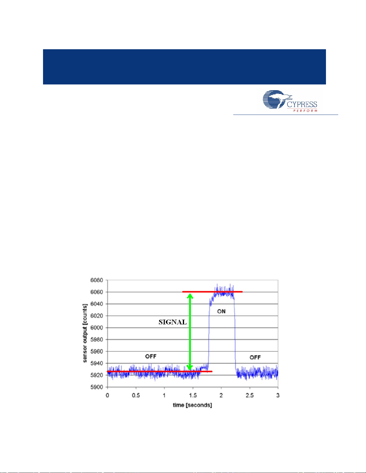
4.1.1.1 CapSense Signal
The CapSense signal is the change in the sensor response when a finger is placed on the sensor, as demonstrated
in Figure 4-1. The output of the sensor is a digital counter with a value that tracks the sensor capacitance. In this
example, the average level without a finger on the sensor is 5925 counts. When a finger is placed on the sensor, the
average output increases to 6060 counts. Because the CapSense signal tracks the change in counts due to the
finger, Signal = 6060 – 5925 = 135 counts.
Figure 4-1. Example of CapSense Signal
CY8C21x34/B CapSense® Design Guide Document No. 001-66271 Rev. *B 29
Page 30
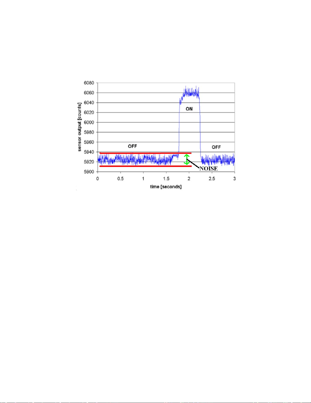
4.1.1.2 CapSense Noise
CapSense noise is the peak-to-peak variation in sensor response when a finger is not present, as shown in
Figure 4-2. In this example, the output waveform without a finger is bounded by a minimum of 5912 counts and a
maximum of 5938 counts. Because the noise is the difference between the minimum and the maximum values of this
waveform, Noise = 5938 – 5912 = 26 counts.
Figure 4-2. Example of CapSense Noise
4.1.1.3 CapSense SNR
CapSense SNR is the simple ratio of signal and noise. Continuing with the example, if the signal is 135 counts and
noise is 26 counts, and then SNR is 135:26, which reduces to an SNR of 5.2:1. The minimum recommended SNR for
CapSense is 5:1, which means the signal is five times larger than the noise. Filters are commonly implemented in
firmware to reduce noise. See Software Filtering for more informat ion.
4.1.2 Charge/Discharge Rate
To achieve maximum sensitivity in the tuning process, the sensor capacitor must be charged and discharged fully
during each cycle. The charge/discharge path switches between two states at a rate set by the Clock parameter in
the User Module.
The charge/discharge path includes series resistance that slows down the transfer of charge. The rate of change for
this charge transfer is characterized by an RC time constant involving the sensor capacitor and series resistance, as
shown in Figure 4-3.
30 Document No. 001-66271 Rev. *B CY8C21x34/B CapSense
®
Design Guide
Page 31
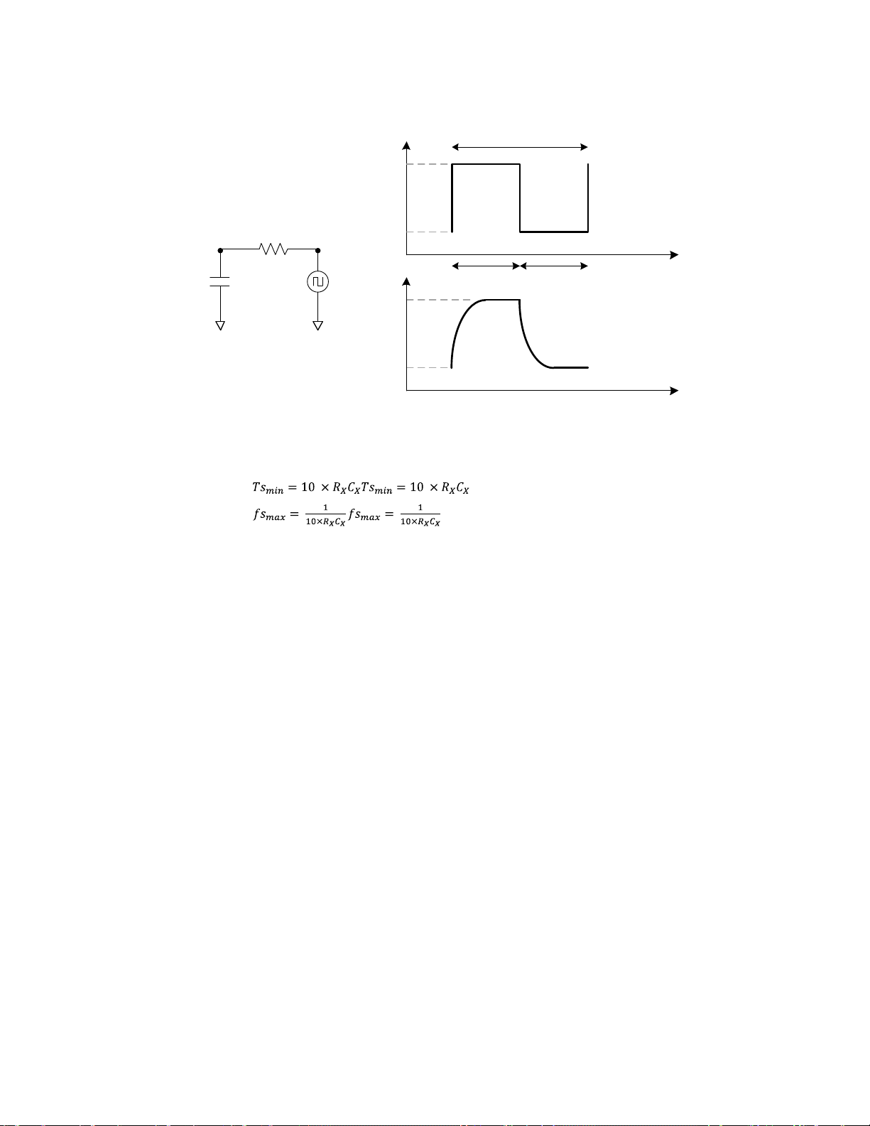
V
s
V
x
Vdd
Vref
Vdd
Vref
t
t
R
x
C
x
V
s
V
x
5*R
x
*C
x
5*R
x
*C
x
Ts
min
>= 10*R
x
*C
x
Figure 4-3. Charge/Discharge Waveforms
Make sure to set the charge/discharge rate to a level that is compatible with this RC time constant. The rule of thumb
is to allow a period of 5RC for each transition, with two transitions per period (one charge, one discharge).The
equations for minimum time period and maximum freq uen cy are:
Equation 5
Equation 6
For example, assume the series resistor includes a 560-Ω external resistor and up to 800 Ω of internal resistance and
the sensor capacitance is typical:
RX = 1.4 kΩ
C
= 24 pF
X
The value of the time constant and maximum front-end switching frequency in this example would be:
Ts
= 0.34 µs
min
fs
= 3 MHz
max
4.1.3 Importance of Baseline Update Threshold Verification
Temperature and humidity both cause the average number of counts to drift over time. The baseline is a reference
count level for CapSense measurements that is an important part of compensating for environmental effects. Highlevel decisions, such as Finger Present and Finger Absent states, are based on the reference level established by the
baseline. Because each sensor has unique parasitic capacitance associated with it, each capacitive sensor has its
own baseline.
Baseline tracks the change in counts at a rate set by the Baseline Update Threshold parameter. Make sure to match
the update rate to the intended application. If the update rate is too fast, the baseline will compensate for any
changes introduced by a finger, and the moving finger will not be detected. If the update rate is too slow, relatively
slow environmental changes may be mistaken for fingers. During development, you should verify the Baseline
Update Threshold settings.
CY8C21x34/B CapSense® Design Guide Document No. 001-66271 Rev. *B 31
Page 32
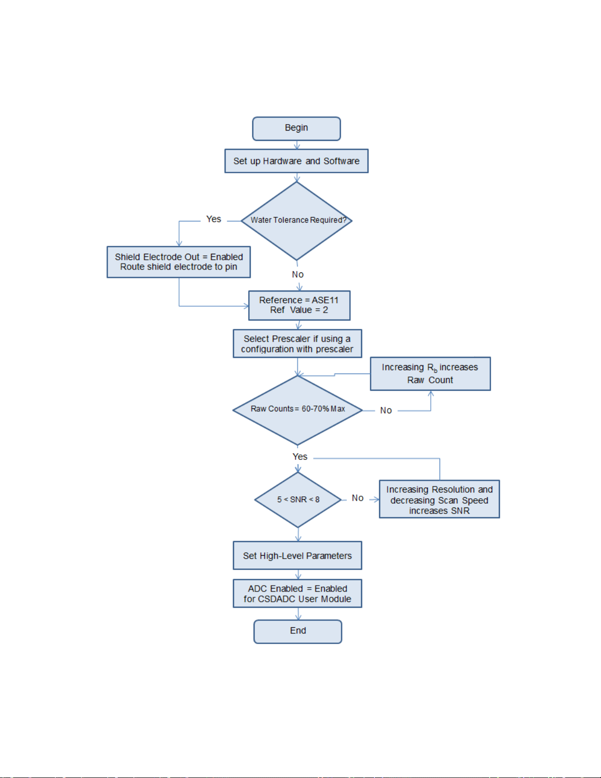
4.2 Tuning the CSD and CSDADC User Modules
Figure 4-4. Tuning CSD and CSDADC User Modules
32 Document No. 001-66271 Rev. *B CY8C21x34/B CapSense
®
Design Guide
Page 33

4.2.1 Set Up Hardware and S o ftw ar e for Tuni ng
Before starting the tuning process, certain hardware and software tools are required. They are listed in the Overview
of CapSense Design Tools. Tuning requires monitoring the raw counts, baseline, and difference counts of the
sensors through a communication interface. A code example that uses an I
communicate with the PC can be downloaded here. After do wnloading the example project:
1. Open the code example using PSoC Designer. In Workspace Explorer, right-click CSD User M odule and select
CSD Wizard. You are shown four CapSense buttons assigned to the pins. Change the number of buttons and
pin assignments according to your application requirements.
2. Change Modulator Capacitor Pin and Feedback Resistor Pin, if required.
3. Generate and build the project.
4. Program the CapSense controller with the hex file.
5. Refer to “Instructions to use USB-I2C Tool to Monitoring CapSense Data” found in the code example’s
documentation for instructions on how to monitor raw count, baseline, and difference count.
2
C communication protocol to
4.2.2 Select Prescaler
To select the Prescaler value, use the following process:
1. Measure the maximum sensor parasitic capacitance using an LCR meter or the CapSense controller. If you are
using an LCR meter, skip to Step 5.
2. Use the CSD User Module with clock prescaler and the following parameters:
a. Scan Speed = Normal
b. Resolution = 16
c. Reference = VBG
d. Prescaler period = 15 (SysClk = 24 MHz), 7 (SysClk = 12 MHz), or 3 (SysClk = 6 MHz)
e. ShieldElectrodeOut = Enable or disable depending on the application
3. Build the project and download it to the CapSense control ler .
4. Monitor only the raw counts from all the sensors (including slider segments) and note the highest raw count
value.
5. Use Equation 7 to calculate m aximum parasitic capacitance.
6. Use Equation 8 to calculate fs
Equation 8
7. Calculate the prescaler value based on the clock configuration.
8. For CSD with the clock prescaler configuration:
max
.
Equation 7
– Equation 9
9. For CSDADC with the PWM8 clock source configuration:
Equation 10
10. For better SNR performance, round the calculated prescaler to the nearest 2n– 1 value (1, 3, 7, 15, 31, and so
on.)
4.2.3 Set Raw Count Range with Rb
The value of the bleed resistor, Rb, determines the sensitivity of the CapSense sensor. Sensitivity is the difference
count measured between a touch and no touch condition. Increasing R
CY8C21x34/B CapSense® Design Guide Document No. 001-66271 Rev. *B 33
improves sensitivity and also increases the
b
Page 34
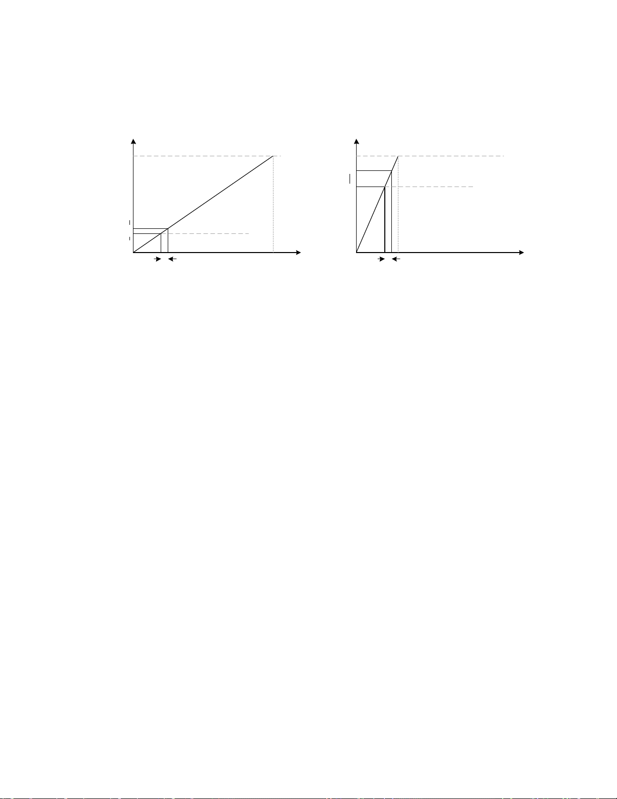
RawCount
C
x
2n-1
RawCount
C
x
2n-1
Change in Cx due
to finger touch
Change in Cx due
to finger touch
Difference
count
Difference
count
70% (2n-1)
Measurement Range with
R
b
1
Measurement Range with
R
b
2 > Rb1
20% (2n-1)
C
xmax1
C
xmax2
raw count value in a no touch condition. Increasing R
also decreases the maximum capacitance value that can be
b
measured by the CapSense sensor.
Figure 4-5. CSD Measurement Range
Consider the two raw count measurement range graphs in Figure 4-5. In the left graph, R
measure capacitance up to C
. The raw count is 20 percent of its maximum value. The difference count produced
xmax1
due to the finger touch is very small, low sensitivity. In the right graph, the bleed resistor is increased, R
= Rb1, the system can
b
2 > Rb1. The
b
raw count is now 70 percent of its maximum. The difference count in this case is much larger than in the first case,
which increases the sensitivity.
Typical values for R
are between 500 Ω and 10 kΩ. To find the optimal resistance:
b
1. Start with a 2-kΩ resistor for Rb.
2. Monitor the raw count measurements for all sensors.
3. Adjust Rb until the raw counts are 70 percent of the full-scale range at the selected scanning resolution. For
example, if 9-bit resolution is selected, the full-scale range is 511 coun ts. R
should be adjusted until the raw
b
data is 358 counts.
In designs with multiple sensors, it can be difficult to set all of the raw counts exactly to 70 percent. In this case, set
all of the raw counts bet w een 60 and 70 per cent of the maximum.
4.2.4 Set High-Level Parameters
Follow the recommendations given in High Level Parame ter R ecom me ndat ion s.
4.3 Configuring SmartSense User Modul e
Here are the basic guidelines for configuring the SmartSense user module in a typical CapSense application:
1. Prepare the target board. Assemble the target application PCB and fix the overlay on it. Use nonconductive glue
or special adhesive tape to stick the overlay. Avoid air gaps between the PCB and the overlay, as it can reduce
the sensitivity substantially and cause multiple false button triggers because of the air gap shifting under the
touch.
2. Set up a real -time data charting tool such as Multi-Chart (Section 3.1.4 ) to monitor one or more data series in
real-time. The sensor rawcount (waSnsResult), baseline (waSnsBaseline), difference counts (waSnsDiff), signal
(baSnsSignal), and button finger threshold (baBtnFThreshold) must be observed during the tuning process. You
can use the UART-USB Bridge or the I2C-USB Bridge hardware to build an interface between CapSense
controller and PC via USB port. Do not use the LCD or any other numerical displays to monitor data, because
they are slow and do not allow visualizing the data dynamics.
3. The default configurations to start with are:
Set IMO = 24 MHz, CPU_Clock = SysClk/1
Place the SmartSense User Module configuration for IMO = 24 MHz
Disable "Sensor Autoreset". Set "Debounce" to 3, and set "Shield Electrode Out" to None.
34 Document No. 001-66271 Rev. *B CY8C21x34/B CapSense
®
Design Guide
Page 35
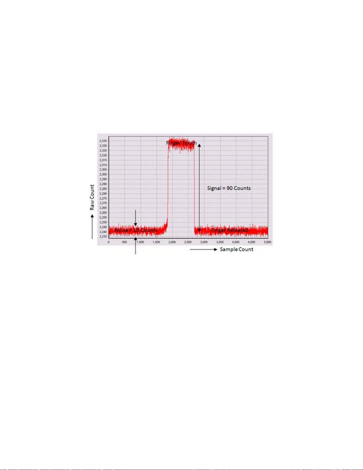
Under Global Settings in the CapSense wizard, assign one sensor under the category "Button". Select the
modulation Capacitor and Feedback resistor pin as well. Set the threshold setting mode as manual, a nd
disable the Median and IIR filters. Ensure that in the board, the Rb value is 15 K and the Cmod is 10 nF.
Under the Sensor Settings tab in CapSense wizard, set "Sensitivity Level" to Low and "Finger Threshold" to
96.
4. Generate/Build the project with the sample firmware code provided in the user module datasheet.
5. Monitor the sensor raw count and calculate the SNR. Figure 4-6 shows the monitored sensor RawCount.
According to CapSense best practices, the SNR for a robust design must be greater than 5. The monitored SNR
in this case is found to be 9, which is above 5. Read SNR improvement techniques in step 7 if the SNR is found
to be less than 5.
Figure 4-6. Monitored Sensor RawCount
6. You can skip this step if precise controlling of finger threshold is not required by the application, or if the
automatic threshold setting mode is selected. The automatic threshold mode uses an algorithm that dynamically
adjusts the finger threshold based on the noise seen in the system. You should choose the manual mode over
the automatic threshold mode under the following scenarios:
If the RAM/ROM footprint is smaller than the number of sensors it must support.
Designs that require precisely adjusted sensor finger thresholds.
Designs that need to be operated under noisy conditions.
If manual threshold setting mode is used, then to complete the tuning process you must set the finger threshold as
well. Monitor the sensor signal baSnsSignal. Determine 80 percent of its maximum value and this value is the finger
threshold. In the example shown in Figure 4-6 it is nearly 100 counts.
CY8C21x34/B CapSense® Design Guide Document No. 001-66271 Rev. *B 35
Page 36

Figure 4-7. Monitoring the Sensor Signal baSnsSignal
Now open the CapSense wizard, and under the Sensor Settings tab set the finger threshold to the calculated value (it
is 100 for the example as shown in Figure 4-7).
7. The SmartSense sensor tuning process is completed with the previous step. However, there could be scenarios
where the SNR achieved in Step 5 is below 5:1, for example, when using a thicker overlay. In such cases, follow
these recommendations:
Change the sensitivity level from "Low" to "Medium". If the SNR of 5:1 is still not achieved, change the level
to "High".
Sometimes, the requirement of 5:1 cannot be achieved due to excess noise observed in the system. Under
these circumstances, software filters should be used. Start with an IIR filter of coefficient 1/2. If this does not
reduce the noise, change the IIR coefficient to 1/4.
36 Document No. 001-66271 Rev. *B CY8C21x34/B CapSense
®
Design Guide
Page 37

5. Design Considerations
When designing capacitive touch sense technology into your application, it is crucial to keep in mind that the
CapSense device exists within a larger framework. Careful attention to every level of detail from PCB layout to user
interface to end-use operating environment will lead to robust and reliable system performance. For more in-depth
information, see Getting Started with CapSense.
5.1 Overla y Selection
In CapSense Fundamentals, Equation 1 was presented for finger capacitanc e as follows:
Where:
ε
= Free space permittivity
0
ε
= Dielectric constant of overlay
r
A = Area of finger and sensor pad overlap
D = Overlay thickness
To increase the CapSense signal strength, choose an overlay material with higher dielectric constant, decrease the
overlay thickness, and increase the button diameter.
Table 5-1. Overlay Material Dielectric Strength
Material Breakdown Voltage (V/mm) Min. Overlay Thickness at 12 kV (mm)
Air 1200–2800 10
Wood – dry 3900 3
Glass – common 7900 1.5
Glass – Borosilicate (Pyrex®)) 13,000 0.9
PMMA Plastic (Plexiglas®) 13,000 0.9
ABS 16,000 0.8
Polycarbonate (Lexan®) 16,000 0.8
Formica 18,000 0.7
FR-4 28,000 0.4
PET Film (Mylar®) 280,000 0.04
Polymide film (Kapton®) 290,000 0.04
Conductive material cannot be used as an overlay because it interferes with the electric field pattern. For this reason,
do not use paints containing metal particles in the overlay.
An adhesive is typically used to bond the overlay to the CapSense PCB. A transparent acrylic adhesive film from
3M™ called 200MP is qualified for use in CapSense applications. This special adhesive is dispensed from paperbacked tape rolls (3M™ product numbers 467MP and 468MP).
CY8C21x34/B CapSense® Design Guide Document No. 001-66271 Rev. *B 37
Page 38

5.2 ESD Protection
Robust ESD tolerance is a natural byproduct of careful system design. By considering how contact discharge will
occur in your end product, particularly in your user interface, it is possible to withstand an 18-kV discharge event
without incurring any damage to the CapSense controller.
CapSense controller pins can withstand a direct 2-kV event. In most cases, the overlay material provides sufficient
ESD protection for the controller pins. Table 5-1 lists the thickness of various overlay materials required to protect the
CapSense sensors from a 12-kV discharge, as specified in IEC 61000-4-2. If the overlay material does not provide
sufficient protection, apply ESD countermeasures in the following order: Prevent, Redirect, Clamp.
5.2.1 Prevent
Make sure that all paths on the touch surface have a breakdown voltage greater than potential high-voltage contacts.
Also, design your system to maintain an appropriate distance between the CapSense controller and possible sources
of ESD. If it is not possible to maintain adequate distance, place a protective layer of a high breakdown voltage
material between the ESD source and CapSense controller. One layer of 5 mil-thick Kapton
18 kV.
5.2.2 Redirect
If your product is densely packed, it may not be possible to prevent the discharge event. In this case, you can protect
the CapSense controller by controlling where the discharge occurs. A standard practice is to place a guard ring on
the perimeter of the circuit board that is connected to the chassis ground. As recommended in PCB Layout
Guidelines, providing a hatched ground plane around the button or slider sensor can redirect the ESD event away
from the sensor and CapSense controller.
®
tape will withstand
5.2.3 Clamp
Because CapSense sensors are purposely placed in close proximity to the touch surface, it may not be practical to
redirect the discharge path. In this case, including series resistors or special-purpose ESD protection devices may be
appropriate.
The recommended series resistance value is 560 Ω.
A more effective method is to provide special-purpose ESD protection devices on the vulnerable traces. ESD
protection devices for CapSense need to be low capacitance. Table 5-2 lists devices recommended for use with
CapSense controllers.
Table 5-2. Low-Capacitance ESD Protection Devices Recommended for CapSense
ESD Protection device
Manufacturer Part Number
Littlefuse SP723 5 pF 2 nA 8 kV 15 kV
Vishay VBUS05L1-DD1 0.3 pF 0.1 µA < ±15 kV ±16 kV
NXP NUP1301 0.75 pF 30 nA 8 kV 15 kV
Input
Capacitance
Leakage
Current
Contact
Discharge
maximum limit
Air Discharge
maximum limit
5.3 Ele c tr om a gne t ic Compatibility (EMC) Consider a ti ons
5.3.1 Radiated Interference
Radiated electrical energy can influence system measurements and potentially influence the operation of the
processor core. Interference may enter the CapSense Controller at the PCB level, through CapSense sensor traces,
and through any other digital or analog inputs. Layout guidelines for minimizing the effects of RF interference include:
Ground Plane: Provides a ground plane on the PCB.
Series Resistor: Place series resistors within 10 mm of the CapSense controller pins.
The recommended series resistance for CapSense input lines is 560 Ω.
38 Document No. 001-66271 Rev. *B CY8C21x34/B CapSense
®
Design Guide
Page 39

The recommended series resistance for communication lines, such as I
2
C, and SPI is 330 Ω.
Trace Length: Minimize trace length whenever possible.
Current Loop Area: Minimize the return path for current. Provide hatched ground instead of solid fill within 1 cm
of the sensors and traces to reduce the impact of parasitic capacitance.
RF Source Location: Partition systems with noise sources such as LCD inverters and switched-mode power
supplies (SMPS) to keep them separated from CapSense inputs. Shielding the power supply is another common
technique for preventing interf erenc e.
5.3.2 Radiated Emissions
To reduce radiated emissions from the CapSense sensor, select a low frequency for the switched capacitor clock.
This clock is controlled in firmware using the Prescaler option. Increasing the Prescaler value decreases the
frequency of the switching clock
5.3.3 Conducted Immunity and Emissions
Noise entering a system through interconnections with other systems is referred to as conducted noise. These
interconnections include power and communication lines. Because CapSense controllers are low-power devices,
conducted emissions must be avoided. The following guidelines will help reduce conducted emission and immunity:
Use decoupling capa cit ors as reco mme nde d by the datash e et.
Add a bidirectional filteron the input to the system power supply. This is effective for both conducted emissions
and immunity. A pi-filter can prevent power-supply noise from effecting sensitive parts, while also preve nting the
switching noise of the part itself from coupling back onto the power planes.
If the CapSense controller PCB is connected to the power supply by a cable, minimize the cable length and
consider using a shielded cable.
You can place a ferrite bead around the power supply or communication lines to filter out high frequency noise.
5.4 Software Filtering
Software filters are one of the techniques for dealing with high levels of system noise. Table 5-3 lists the types of
filters that have been found useful for CapSense.
Table 5-3. Table of CapSense Filters
Type Description Application
Average Finite impulse response filter (no feedback) with
equally weighted coefficients
IIR Infinite impulse response filter (feedback) with a
step response similar to an RC filter
Median Nonli near filter that computes median input value
from a buffer of size N
Jitter Nonlinear filter that limits current input based on
previous input
Event-Based Nonlinear filter that causes a predefined
response to a pattern observed in the sensor
data
Rule-Based Nonlinear filter that causes a predefined
response to a pattern observed in the sensor
data
A code example that uses all the above listed filters can be downloaded here.
Periodic noise from power supplies
High-frequency white noise (1/f noise)
Noise spikes from motors and switching power supplies
Noise from thick overlay (SNR < 5:1), especially useful for
slider centroid data
Commonly used during nontouch events to block CapSense
data transmission
Commonly used during normal operation of the touch surface
to respond to special scenarios such as accidental
multibutton selection
CY8C21x34/B CapSense® Design Guide Document No. 001-66271 Rev. *B 39
Page 40

Table 5-4 shows the RAM and flash requirements for different software filters. The amount of flash required for each
filter type depends on the performance of the compiler. The requirements listed here are for both the ImageCraft
compiler and the ImageCraft Pro compiler
Table 5-4. RAM and Flash Requirements
Filter Type Filter Order RAM
(Bytes per
sensor)
Average 2-8 6 675 665
IIR 1 2 429 412
2 6 767 622
Median 3 6 516 450
5 10 516 450
Jitter filter on Raw Counts N/A 2 277 250
Jitter filter on slider centroid N/A 2 131 109
Flash (Bytes)
ImageCraft
Compiler
Flash (Bytes)
ImageCraft Pro
Compiler
A code example that uses all of the filters listed above can be downloaded here.
5.5 Pow er Cons um pt ion
5.5.1 System Design Recommendations
For many designs, minimizing power consumption is an important goal. There are several ways to reduce the power
consumption of your CapSense capacitive touch-se ns ing sy s tem.
Set GPIO drive mode for low power
Turnoff high power blocks
Optimize CPU speed for low power
Operate at a lower V
DD
In addition to these methods, applying the sleep-scan method can be very effective.
5.5.2 Sleep-Scan Method
In typical applications, the CapSense controller does not always need to be in the active state. The device can be put
into the sleep state to stop the CPU and the major blocks of the device. Current consumed by the device in sleep
state is much lower than the active current.
The average current consumed by the device over a long time period can be calculated by using the following
equation.
Equation 11
Where:
I
= active current
ACT
T
= active time
ACT
I
= sleep current
Slp
= seep time
t
Slp
T = total time period
40 Document No. 001-66271 Rev. *B CY8C21x34/B CapSense
®
Design Guide
Page 41
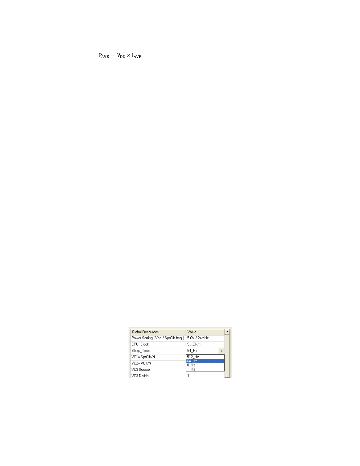
The average power consumed by the device can be calculated as follows:
Equation 12
Where:
V
= supply voltage
DD
= average current
I
AVE
An Excel-based average power consumption calculator is available. Click here to download the calculator.
5.5.3 Response Time versus Power Consumption
As illustrated in Equation 12, the average power consumption can be reduced by decreasing I
or VDD. I
AVE
may be
AVE
decreased by increasing sleep time. Increasing sleep time to a very high value will lead to poor response time of the
CapSense button. As a result, the sleep time must be based on system requirements.
In any application, if both power consumption and response time are important parameters to be considered, then
you can use an optimized method incorporates both continuous-scan and sleep-scan modes. In this method, the
device spe nds most of its time in sleep-scan mode, where it scans the sensors and goes to sleep periodically, as
explained in the previous section, thereby consuming less power. When a user touches a sensor to operate the
system, the device jumps to continuous-scan mode, where the sensors are scanned continuously without invoking
sleep, giving very good response time. The device remains in continuous-scan mode for a specified timeout period. If
the user does not operate any sensor within this timeout period, the device jumps back to the sleep-scan mode.
5.5.4 Measuring Average Power Consumption
The following instructions describe how to determine average power consumption when using the sleep-scan
method:
1. Build a project that scans all of the sensors without going to sleep (continuous-scan mode). Include a pin-toggle
feature in the code before scanning the sensors. Toggling the state of the output pin serves as a time marker that
can be tracked with a scope.
2. Download the project to the CapSense device and measure the current consumption. Assign the measured
current to I
3. Get the sleep current information from the datasheet and assign it to I
4. Monitor the toggling output pin with an oscilloscope and measure the time period between two toggles. This
gives the active time. Assign this value to t
5. Apply sleep-scan to the project. The time period of the sleep-scan cycle, T, is set by selecting the sleep timer
frequency in the global resources window, as shown in Figure 5-1.
6. Subtract active time from the sleep-scan cycle time period to get the sleep time. t
7. Calculate the average current using Equation 11.
8. Calculate average power consumption using Equation 12.
ACT
.
.
Slp
.
Act
= T - t
Slp
Act
.
Figure 5-1. Global Resources Window
CY8C21x34/B CapSense® Design Guide Document No. 001-66271 Rev. *B 41
Page 42
5.6 Pin Assignments
An effective method to reduce interaction between CapSense sensor traces and communication and non-CapSense
traces is to isolate each by port assignment. Figure 5-2 shows a basic version of this isolation for a 32-pin QFN
package. Because each function is isolated, the CapSense controller is oriented such that there is no crossing of
communication, LED, and sensing traces.
Figure 5-2. Recommended: Port Isolation for Communication, CapSense, and LEDs
CapSense controller architecture requires a current budget for even and odd port pin numbers. If the current budget
for odd port pin numbers is 100 mA, the total current drawn though all odd port pins should not exceed 100 mA. In
addition to the current budget limitation, there is also maximum current limitation for each port pin defined in the
CapSense controller datasheet.
All CapSense controllers provide high current sink and source capable port pins. When using high current sink or
source from port pins, you should use the ports that are closest to device ground pin to minimize the noise.
5.7 PCB Layout Guidelines
Detailed PCB layout guidelines are available in Getting Started with CapSense.
42 Document No. 001-66271 Rev. *B CY8C21x34/B CapSense
®
Design Guide
Page 43
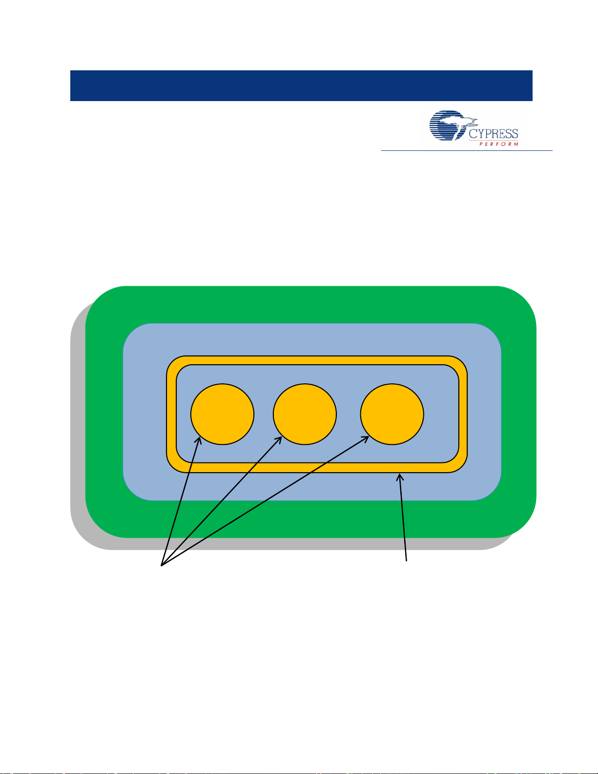
6. W ater Tolerance
PCB
Shield Electrode
Guard Sensor
Sensor Pads
Some CapSense capacitive touch-sensing applications require reliable operation in the presence of water. White
goods, automotive applications, and industrial applications are examples of systems that must perform in
environments that include water, ice, and humidity changes. For such applications, shield electrodes and guard
sensors can provide robust touch sensing.
6.1 Shie ld Electrode and Guard Sensor
Figure 6-1. PCB Layout with Shield Electrode and Guard Sensor
6.1.1 Shield
Shield electrodes protect CapSense button sensors from detecting false touches caused by water drops. When water
drops are present on the overlay surface, the coupling between the shield electrode and sensor pad is increased by
, as shown in Figure 6-2.
C
WD
CY8C21x34/B CapSense® Design Guide Document No. 001-66271 Rev. *B 43
Page 44

Figure 6-2. Capacitance Measurement with Water Drop
C
The purpose of the shield electrode is to set up an electric field around the touch sensors that helps attenuate the
effects of water. The shield electrode works by mirroring the voltage of the touch sensor on the shield.
Follow these guidelines to ensure proper shield operatio n:
– Capacitance between the water drop and shield electrode
WD
Schematic
Layout
Firmware Development
6.1.1.1 Schematic
Select the proper pin to drive the shield electrode out signal. The following pins should NOT be used to drive the
shield electrode out signal.
Modulator capacitor pin (C
Feedback resistor pin (R
): P0[1] or P0[3]
MOD
): P1[1] or P1[5]
B
Other port pins: P0[0], P0[4], P1[0], P1[4], P2[0], P2[4], and P3[0]
6.1.1.2 Layout
Follow the layout guidelines given in Getting Started with CapSense.
6.1.1.3 Firmw are Development
Step 1: Select the shield electrode signal source from one of the free digital row buses (Row_0_Output_1 to
Row_0_Output_3):
Select Row_0_Output_1 if shield pin is P0[5], P1[5], P2[1], P2[5]
Select Row_0_Output_2 if shield pin is P0[2], P0[6],P1[2], P1[6], P2[2], P2[6], P3[2]
Select Row_0_Output_3 if shield pin is P0[7],P1[3], P1[7], P2[3], P2[7]
Step 2: Route the shield electrode out to the shield pin. Follow these steps:
1. Select the shield electrode out.
2. Route the Row output signal to Global out Odd/Even.
3. Connect the Global out Odd/Even to Port pin. For example, if P0[2] is selected as the shield pin:
From the user module properties, select the shield electrode out on Select Row_0_Output_2.
4. Click on Row_0_Output_2 and open the digital interconnect view as shown in Figure 6-3.
44 Document No. 001-66271 Rev. *B CY8C21x34/B CapSense
®
Design Guide
Page 45

Figure 6-3. Schematic View of Digital Interconnect
5. Select Row_0_Output_2_Drive_0 and select GlobalOutEven_2 as shown in Figure 6-4.
Figure 6-4. Schematic View of Output Select
6. Click on GlobalOutEven_2 and select P0{2] in the Pin option as shown in the following figure.
CY8C21x34/B CapSense® Design Guide Document No. 001-66271 Rev. *B 45
Page 46

PCB
Shield Electrode
Guard Sensor
Sensor Pads
6.1.2 Guard Sensor
Figure 6-5. PCB with Shield and Guard Sensor
46 Document No. 001-66271 Rev. *B CY8C21x34/B CapSense
®
Design Guide
Page 47

A guard sensor is a copper trace, as shown in Figure 6-5, that surrounds all the sensors on the PCB, which is used to
detect the presence of a continuous water stream. When a water stream is present on the sensing surface, a largecapacitance C
CWD. Because of this, the effect of the shield electrode is completely masked and the raw counts measured by the
sensor will be the same as or even higher than a finger touch. In this situation, a guard sensor will help; when it
detects a water stream, it will block the other sensors from triggering.
is added to the system, as shown in Figure 6-6. This capacitance may be several times larger than
ST
Figure 6-6. Capacitance Measurement with Water Stream
C
C
C
- Capacitance between the water stream and shield electrode.
WD
- Capacitance between the water stream and the system ground.
ST
- Capacitance between the water stream and the guard sensor
WG
The guard sensor should be implemented in firmw are. One CapSense pin and a counter (hardware/software) are
required to implement the guard sensor.
When a water stream is applied to the board, the guard sensor detects this event and disables the touch sensor
processing logic. Additional guard sensor "dead" time prevents unlocking the sensor prematurely. When the water
stream is gone, the guard counter suppresses touch processing for a short time (Guard Sensor counter). This
eliminates false touch detection from any water that remains on the board.
Figure 6-7
is a flowchart that shows how the guard sensor should be implemented in firmware.
CY8C21x34/B CapSense® Design Guide Document No. 001-66271 Rev. *B 47
Page 48
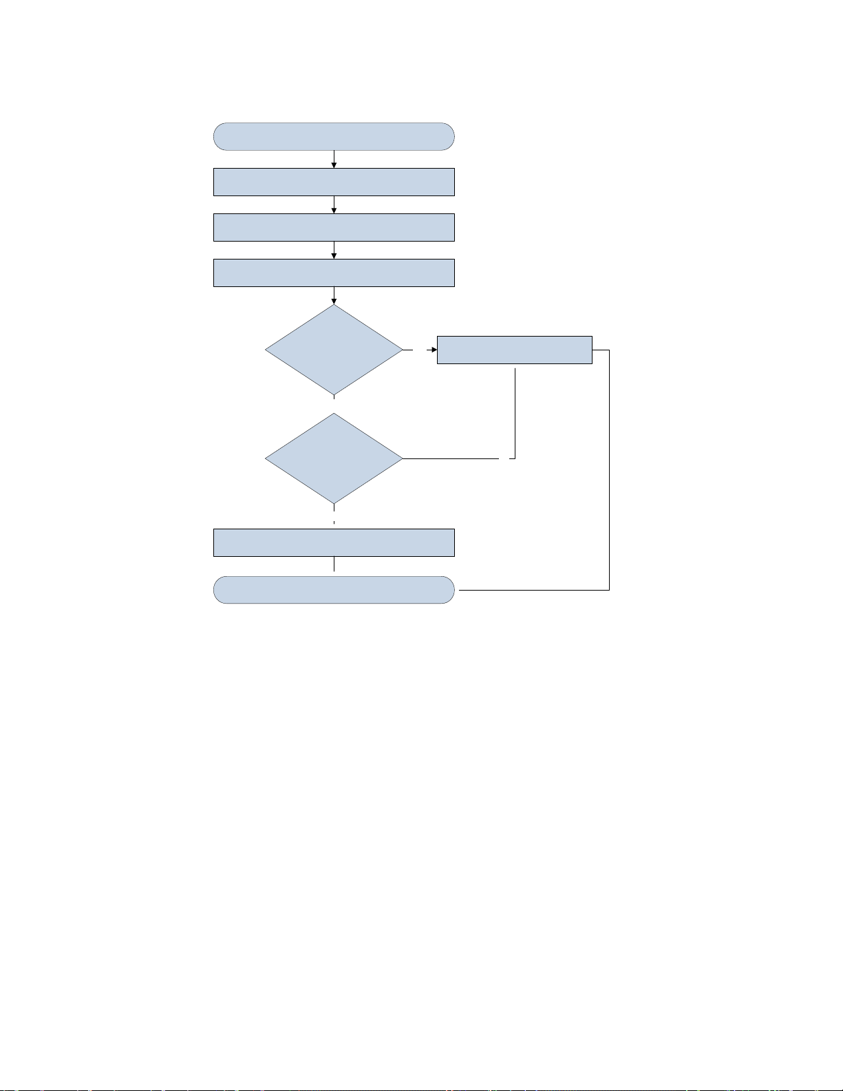
Start of main function
End of main function
Initialize CapSense block and other blocks
Scan all sensors including Guard sensor
Update baseline of all sensors
Is Guard Sensor ON? Turn off all the sensors
Guard sensor
counter elapsed?
Report sensor status normally
Yes
No
No
Yes
Figure 6-7. Flow Chart to Implement the Guard Sensor
6.2 Desi gn Re c om m endations
The following system-level and PCB layout recommendations apply to CapSense systems that will be exposed to
water:
Shield-electrode copper-hatch recommendations:
Top layer – 7-mil trace and 45-mil grid (15-percent fill)
Bottom layer – 7-mil trace and 70-mil grid (10-percent fill)
The shield electrode between buttons should be at least 10 mm wide
Only areas surrounding sensor pads and the CapSense controller should be grounded
Place sensor surface vertically or at an angle to the horizontal so that water drops naturally move off the sensors
and large water drops do not accumulate.
Use water-repellent and nonabsorbent overlay material. This minimizes water streaks and films on the device
panel. This is especially important if the water is highly conductive, such as seawater.
You must use a guard sensor in situations where the application may be subjected to continuous water streams.
A guard sensor is not required if the device will be subjected only to rain.
48 Document No. 001-66271 Rev. *B CY8C21x34/B CapSense
®
Design Guide
Page 49

7. Proximity Sensing
Proximity Sensor
Proximity sensors detect the presence of a hand or other conductive object before it makes contact with the
capacitive touch surface. Imagine a hand stretched out to operate a car audio system in the dark. Proximity detect i on
enables the system to light up with the approach of a finger. For example, the buttons of an audio system will glow
with its backlight LEDs when the user's hand is near.
7.1 Types of Proximity Sensors
7.1.1 Button
A button with large CP and small difference counts can work as a proximity sensor. The sensitivity of a proximity
sensor implemented as a button is much higher than a regular capacitive touch-sensing button.
7.1.2 Wire
A single length of wire works well as a proximity sensor. Because detecting a hand relies on the capacitance change
from electric field changes, any stray capacitance or objects affecting the electrical field around the wire will affect the
range of the proximity sensor. Using a wire sensor is not an optimal solution for mass production because of
manufacturing cost and complex ity.
7.1.3 PCB Trace
A long PCB trace can form a proximity sensor. The trace can be a straight line, or i t can surround the perimeter of a
system’s user interface, as shown in Figure 7-1. This method is appropriate for mass production, but it is not as
sensitive as a wire sensor.
Figure 7-1. Proximity Sensor Using PCB Trace
7.1.4 Sensor Ganging
Another way to implement a proximity sensor is to gang sensors together. This is accomplished by combining
multiple sensors into one large sensor, using firmware to connect the sensors from the internal analog multiplexer
bus in PSoC Designer. Be careful not to exceed the C
CY8C21x34/B CapSense® Design Guide Document No. 001-66271 Rev. *B 49
limit of your design when using this method.
P
Page 50

7.2 Desi gn Re c om m endations
Using a shield electrode effectively extends the detection distance of the proximity sensor. This is particularly helpful
when the proximity sensor must operate in the presence of metal.
A wire sensor increases the beneficial effect of the shield electrode because it can be located farther from the shield
electrode.
Avoid large, solid ground-fill areas inside the proximity sensor, because this decreases the sensitiv ity .
Slower scan speeds provide increased sensitivity at all distances. For a proximity sensor, the scanning speed should
be very slow.
50 Document No. 001-66271 Rev. *B CY8C21x34/B CapSense
®
Design Guide
Page 51

8. Low Power Design Considerations
Power consumption is an important aspect of microcontroller designs. Among the several techniques to reduce the
average current used by the CapSense controller, sleep mode is the most popular. The CapSense controller uses
sleep mode when it is not required to perform any function, similar to a cell phone backlight dimming after an idle
period. This is done to reduce the average current consumed by the device, a necessity of all battery applications.
The CapSense controller enters sleep mode by writing a ‘1’ to the SLEEP bit within the CPU_SCR0 register (Bit 3).
This is accomplished by calling the M8C_Sleep macro. While in sleep mode, the central CPU is stopped, the internal
main oscillator (IMO) is disabled, the Bandgap Voltage reference is powered down, and the Flash Memory Model is
disabled. The only circuits left in operation are supply voltage monitor and 32-kHz internal oscillator. Power saving
techniques other than sleep mode are:
Disable CapSense (PSoC) analog block references
Disable continuous time (CT) and switch capacitor (SC) blocks
Disable CapSense (PSoC) analog output buffers
Set drive modes to analog HI-Z
Sleep mode has negative effects for a design. If not used carefully, it can cause unpredictable operation. The PSoC
must be correctly awakened from sleep when necessary, and the user must be aware that the device is sleeping to
allow extra processing.
8.1 Additional Power Saving Techniques
All of the power saving techniques, with the exception of sleep mode, are application based and some of these
produce undesirable results. Each technique is discussed in detail below.
ABF_CR0 &= 0xc3; // Buffer Off
8.1.1 Set Drive Modes to Analog HI-Z
The state of the CapSense controller drive modes can affect power consumption. You can change the drive modes
only on pins that do not cause adverse affects to the system. The change must occur in a sequence that does not
produce line glitches. This sequence depends on the current drive mode of the pin and the state of port data register.
With the CapSense controller drive mode structure, the pin must temporarily be in either Resistive Pull-up or
Resistive Pull-down drive mode when switching between HI-Z or Strong drive modes. The temporary drive mode is
the opposite of the previous value on the pin. So, if the pin was driven high, then the temporary drive mode must be
Resistive Pull-down. This ensures that the drive mode of the pin is not resistive, which eliminates any possible glitch.
The drive modes are set manually in software, before going to sleep. There are three registers, PRTxDM0,
PRTxDM1, and PRTxDM2, which control the drive modes. One bit per register is assigned to a pin. So, to change the
drive mode of a single pin, three register writes are needed. However, this is convenient because an entire port is
changed by the same three register writes. The correct pit pattern for Analog HI-Z is 110b. Use the following code to
set port zero to Analog HI-Z, from Strong, by first going to Resistive Pull-down.
PRT0DM0 = 0x00; // low bits
PRT0DM1 = 0xff; // med bits
PRT0DM2 = 0xff; //high bits
CY8C21x34/B CapSense® Design Guide Document No. 001-66271 Rev. *B 51
Page 52

8.1.2 Putting it All Together
The following code is a sample of a typical sleep preparation sequence for a 28-pin part. In this sequence, interrupts
are disabled, the analog circuitry is turned off, all drive modes are set to Analog HI-Z, and interrupts are re-enabled.
void PSoC_Sleep(void){
M8C_DisableGInt;
ARF_CR &= 0xf8; // analog blocks Off
ABF_CR0 &= 0xc3; // analog buffer off
PRT0DM0 = 0x00; // port 0 drives
PRT0DM1 = 0xff;
PRT0DM2 = 0xff;
PRT1DM0 = 0x00; // port 1 drives
PRT1DM1 = 0xff;
PRT1DM2 = 0xff;
PRT2DM0 = 0x00; // port 2 drives
PRT2DM1 = 0xff;
PRT2DM2 = 0xff;
M8C_EnableGInt;
M8C_Sleep;
}
8.1.3 Sleep Mode Complications
The CapSense controller can exit sleep either from a reset or through an interrupt. There are three types of resets
within the CapSense controller: External Reset, Watchdog Reset, and Power-On Reset. Any of these resets takes the
CapSense controller out of sleep mode, and once the reset deasserts, the CapSense controller begins executing
code starting at Boot.asm. Available interrupts to wake the CapSense controller are: Sleep Timer, Low-Voltage
Monitor, GPIO, Analog Column, and Asynchronous. Sleep mode complications arise when using interrupts to wake
the CapSense controller or attempting digital communication while asleep. These considerations are discussed in
detail in the following sections.
8.1.4 Pending Interrupts
If an interrupt is pending, enabled, and scheduled to take after a write to the SLEEP bit in the CPU_SCR0 register,
the system will not go to sleep. The instruction still executes, but the CapSense controller does not set the SLEEP bit.
Instead, the interrupt is serviced, which effectively causes the CapSense controller to ignore the sleep instruction. To
avoid this, interrupts should be globally disabled while sleep preparation occurs and then re-enabled just before
writing the SLEEP bit.
8.1.5 Global Interrupt Enable
The Global Interrupt Enable register (CPU_F) need not be enabled to wake the CapSense controller from interrupts.
The only requirement to wake up from sleep by an interrupt is to use the correct interrupt mask within the INT_MSKx
registers, as in the example below. If global interrupts are disabled, the ISR that wakes the CapSense controller is not
executed but the CapSense controller still exits sleep mode.
In this case, you must manually clear the pending interrupt or enable global interrupts to allow the ISR to be serviced.
Interrupts are cleared within the INT_CLRx registers.
//Set Mask for GPIO Interrupts M8C_EnableIntMask(INT_MSK0, INT_MSK0_GPIO)
// Clear Pending GPIO Interrupt
INT_CLR0 &= 0x20;
52 Document No. 001-66271 Rev. *B CY8C21x34/B CapSense
®
Design Guide
Page 53

8.2 Post Wakeup Execution Sequence
If the CapSense controller is awakened through a reset, then execution starts at the beginning of the boot code. If the
CapSense controller is awakened by an interrupt service routine, the first instruction to execute is the one
immediately following the sleep instruction. This is because the instruction immediately following the sleep instruction
is prefetched before the CapSense controller is fully asleep. Therefore, if global interrupts are disabled, the instruction
execution will continue where it left off before sleep was initiated.
8.2.1 PLL Mode Enabled
If PLL mode is enabled, the CPU frequency must be reduced to the minimum of 3 MHz before going to sleep. This is
because the PLL always overshoots as it attempts to relock after the CapSense controller wakes up and is reenabled. Additionally, you should wait 10 ms after wakeup before normal CPU operation begins to ensure proper
execution. This implies that, to use sleep mode and the PLL, the software must be able to execute at 3 MHz. A
simple write to the OSC_CR0 register can reduce CPU speed. However, this register just sets a divider of SYSCLK,
which means that the CPU speed will vary between part families with different SYSCLKs. Typically, SYSCLK is
24 MHz
OSC_CR0 &= 0xf8; // CPU = 3 IMO = 24
8.2.2 Execution of Global Interrupt Enable
It is not desirable to get an interrupt on the instruction boundary of writing the SLEEP bit. This could cause all
firmware preparations for going to sleep to be bypassed, if a sleep command is executed on a return from interrupt
(reti) instruction. To prevent this, interrupts are temporarily disabled before sleep preparations and then re-enabled
before going to sleep. Because of the timing of the Global Interrupt instruction, an interrupt cannot occur during the
next instruction, which in this case is setting the SLEEP bit.
8.2.3 I2C Slave with Sleep Mode
There are a few complications using an I2C Slave in sleep mode. Because the IMO and CPU are shut off during
sleep, there is no processing within the CapSense controller. The problem arises with the I
START condition is sent to a particular address, the CapSense controller cannot process the address and therefore
responds with a NAK. A typical workaround is to set up falling edge interrupts on either the clock or data lines of the
2
C bus. The master can then send a dummy START condition to wake up the CapSense controller. There is some
I
lag time between waking up and being able to process an I
before the next transmission or continue to send until an ACK is received. This solution has a second problem in that
the CapSense controller will wake up on any I
sleep currents. Another solution is to use a third GPIO pin to wake up the CapSense controller and then send the
initial START condition after the appropriate delay time.
2
C falling edge traffic, which causes more total active time and higher
2
C address, so the master may need to delay up to 200 µs
2
C address. W hen an I2C
8.2.4 Sleep Timer
The CapSense controller offers a sleep timer and a Sleep Timer User Module. These are used while CapSense
controller is asleep and both perform similar functions. The actual sleep timer runs off of the internal low-speed
oscillator, which is never turned off. At selectable intervals of 1 Hz, 8 Hz, 64 Hz, and 512 Hz, the timer generates an
interrupt. It is often useful to periodically wake the CapSense controller up to do some processing or check for
activity. An example of this would be to periodically wake up to scan a sensor. The Sleep Timer User Module uses
the sleep timer to generate some additional functionality. This functionality includes a background tick counter to
generate periodic interrupts, a delay function for program loops, a settable down counter, and a loop governor to
control loop time. A simple block diagram for this functionality is shown in Figure 8-1.
CY8C21x34/B CapSense® Design Guide Document No. 001-66271 Rev. *B 53
Page 54

Figure 8-1. Sleep Timer User Module Block Diagram
54 Document No. 001-66271 Rev. *B CY8C21x34/B CapSense
®
Design Guide
Page 55

9. Resources
9.1 Website
The Cypress CapSense Controllers website gives access to all of the reference material discussed in this section.
The CY8C21x34/B web page has a variety of technical resources for the CapSense CY8C21x34/B family of devices.
9.2 Datasheet
The datasheet for the CapSense CY8C21x34/B family of devices is available at www.cypress.com.
CY8C21234, CY8C21334, CY8C21434, CY8C21534, CY8C21634
CY8C21234B, CY 8C21334B , CY8C21434B, CY8C21534B, CY8C21634B
9.3 Techn ical Reference Manual
Cypress has created the following technical reference manual to provide quick and easy access to information on
CapSense controller functionality, including top-level architectural diagrams, registers, and timing diagrams.
CY8CPLC20, CY8CLED16P01, CY8C29x66, CY8C27x43, CY8C24x94, CY8C24x23, CY8C24x23A,
CY8C22x13, CY8C21x34, CY8C21x23, CY7C64215, CY7C603xx, CY8CNP1xx, and CYWUSB6953 PSoC(R)
Programmable System-on-Chip Technical Reference Manual (TRM)
9.4 Developm e nt Kits
9.4.1 Universal CapSense Controller Kit
Universal CapSense Controller Kits feature predefined control circuitry and plug-in hardware to make prototyping and
debugging easy. Programming and I
CY3280-BK1 Universal CapSense Controller
9.4.2 Universal CapSense Module Boards
9.4.2.1 Simple Butt on Module Board
The CY3280-BSM Simple Button Module consists of ten CapSense buttons and ten LEDs. This module connects to
any CY3280 Universal CapSense Controller Board.
2
C-to-USB Bridge hardware are included for tuning and data acquisition.
9.4.2.2 Matrix Button Module Board
The CY3280-BMM Matrix Button Module consists of eight LEDs and eight CapSense sensors organized in a 4×4
matrix format to form 16 physical buttons. This module connects to any CY3280 Universal CapSense Controller
Board.
CY8C21x34/B CapSense® Design Guide Document No. 001-66271 Rev. *B 55
Page 56

9.4.2.3 Linear Slider Module Board
The CY3280-SLM Linear Slider Module consists of five CapSense buttons, one linear slider (with ten sensors), and
five LEDs. This module connects to any CY3280 Universal CapSense Controller Board.
9.4.2.4 Radial Slider Module Board
The CY3280-SRM Radial Slider Module consists of four CapSense buttons, one radial slider (with ten sensors), and
four LEDs. This module connects to any CY3280 Universal CapSense Controller Board.
9.4.2.5 Universal CapSense Prototyping Module
The CY3280-BBM Universal CapSense Prototyping Module provides access to every signal routed to the 44-pin
connector on the attached controller boards. The Prototyping Module board is used in conjunction with a Universal
CapSense Controller board to implement additional functionality that is not part of the other single-purpose Universal
CapSense Module boards.
9.4.3 In-Circuit Emulation (ICE) Kit
The ICE pod provides the interconnection between the CY3215-DK In-Circuit Emulator and the target PSoC device in
a prototype system by way of a flex cable or PCB through package-specific pod feet. The following pod is available:
CY3250-21X34QFN In-Circuit Emulation (ICE) Pod Kit for Debugging QFN CY8C21x34 PSoC Devices
9.5 PSoC Programmer
PSoC Programmer is a flexible, integrated programming application for programming PSoC devices.
PSoC Programmer can be used with PSoC Designer and PSoC Creator to program any design onto a PSoC device.
PSoC Programmer provides a hardware layer with APIs to design specific applications that use the programmers and
bridge devices. The PSoC Programmer hardware layer is fully detailed in the COM guide documentation as well as
the example code across the following languages: C#, C, Perl, and Python.
9.6 MultiChart
MultiChart is a simpl e PC tool for real-time CapSense data viewing and logging. The application allows you to view
data from up to 48 sensors, save and print charts, and save data for later analy s is in a spreads heet.
9.7 PSoC Des igner
Cypress offers an exclusive Integrated Design Environment, PSoC Designer. With PSoC Designer, you can configure
analog and digital blocks, develop firmware, and tune your design. Applications are developed in a drag-and-drop
design environment using a library of precharacterized analog and digital functions, including CapSense.
PSoC Designer comes with a built-in C compiler and an embedded programmer. A pro compiler is available for
complex designs.
9.8 Code Exa m ples
Cypress offers a large collection of code examples to get your design up and running fast.
Power Consumption With CapSense (CSD) on CY8C21x34 Device - EP65489
CSD Software Filters with EzI2Cs Slave on CY8C21x34
Interfacing PSoC to an SPI EEPROM
CSD with EzI2Cs Slave on CY8C21x34
Pseudo Random Sequence Generator
CSD with TX8 on CY8C21x34
CSD with I2CHW Slave on CY8C21x34
56 Document No. 001-66271 Rev. *B CY8C21x34/B CapSense
®
Design Guide
Page 57

CMPPRG User Module Example
Receive String using CYRF6936 and CY8C27643
CapSense Sigma Delta (CSD) with LED Backlight Fading on CY8C21x34
CSD with SPIS on CY8C21x34
9.9 Desi gn S upport
Cypress has many design sup port channels to ensure the success of your CapSense solutions.
Knowledge Base Articles –Browse technical articles by product family or perform a search on various CapSense
topics.
CapSense Application Notes –Refer to a wide variety of application notes built on information presented in this
document.
White Papers – Learn about advanced capacitive touch interface topics.
Cypress Developer Community – Connect with the Cypress technical community and exchange information.
CapSense Product Selector Guide – See the complete product offering of the Cypress CapSense product line.
Video Library – Quickly get up to speed with tutorial videos.
Quality & Reliability – Cypress is committed to complete customer satisfaction. At our Quality website, you can
find reliability and product qualification reports.
Technical Support – World-class technical support is available online.
9.10 Document Revision History
Revision Issue Date Origin of Change Description of Change
** 12/29/2010 ANBA New Design Guide
*A 3/3/2011 ARVM Multiple chapter enhancements for content and reader
*B 12/07/2011 MATT Added bull et ed abstrac t
clarity
Added Section 1.2
Moved Document Revision History to end of document
Rewrote Section 2 for clarity
Updated SmartSense tuning
Added Water Tolerance and Proximity Sensing
Added Low Power
CY8C21x34/B CapSense® Design Guide Document No. 001-66271 Rev. *B 57
 Loading...