

Page 1

AN64846
Getting Started with CapSense
®
Document No. 001-64846 Rev. *X
Cypress Semiconductor
198 Champion Court
San Jose, CA 95134-1709
http://www.cypress.com
Page 2

Copyrights
AN64846 - Getting Started with CapSense® Doc. No. 001-64846 Rev. *X 2
Copyrights
© Cypress Semiconductor Corporation, 2010-2018. This document is the property of Cypress Semiconductor Corporation
and its subsidiaries, including Spansion LLC (“Cypress”). This document, including any software or firmware included or
referenced in this document (“Software”), is owned by Cypress under the intellectual property laws and treaties of the
United States and other countries worldwide. Cypress reserves all rights under such laws and treaties and does not, except
as specifically stated in this paragraph, grant any license under its patents, copyrights, trademarks, or other intellectual
property rights. If the Software is not accompanied by a license agreement and you do not otherwise have a written
agreement with Cypress governing the use of the Software, then Cypress hereby grants you a personal, non-exclusive,
nontransferable license (without the right to sublicense) (1) under its copyright rights in the Software (a) for Software
provided in source code form, to modify and reproduce the Software solely for use with Cypress hardware products, only
internally within your organization, and (b) to distribute the Software in binary code form externally to end users (either
directly or indirectly through resellers and distributors), solely for use on Cypress hardware product units, and (2) under
those claims of Cypress’s patents that are infringed by the Software (as provided by Cypress, unmodified) to make, use,
distribute, and import the Software solely for use with Cypress hardware products. Any other use, reproduction,
modification, translation, or compilation of the Software is prohibited.
TO THE EXTENT PERMITTED BY APPLICABLE LAW, CYPRESS MAKES NO WARRANTY OF ANY KIND, EXPRESS
OR IMPLIED, WITH REGARD TO THIS DOCUMENT OR ANY SOFTWARE OR ACCOMPANYING HARDWARE,
INCLUDING, BUT NOT LIMITED TO, THE IMPLIED WARRANTIES OF MERCHANTABILITY AND FITNESS FOR A
PARTICULAR PURPOSE. No computing device can be absolutely secure. Therefore, despite security measures
implemented in Cypress hardware or software products, Cypress does not assume any liability arising out of any security
breach, such as unauthorized access to or use of a Cypress product. In addition, the products described in these materials
may contain design defects or errors known as errata which may cause the product to deviate from published
specifications. To the extent permitted by applicable law, Cypress reserves the right to make changes to this document
without further notice. Cypress does not assume any liability arising out of the application or use of any product or circuit
described in this document. Any information provided in this document, including any sample design information or
programming code, is provided only for reference purposes. It is the responsibility of the user of this document to properly
design, program, and test the functionality and safety of any application made of this information and any resulting product.
Cypress products are not designed, intended, or authorized for use as critical components in systems designed or intended
for the operation of weapons, weapons systems, nuclear installations, life-support devices or systems, other medical
devices or systems (including resuscitation equipment and surgical implants), pollution control or hazardous substances
management, or other uses where the failure of the device or system could cause personal injury, death, or property
damage (“Unintended Uses”). A critical component is any component of a device or system whose failure to perform can
be reasonably expected to cause the failure of the device or system, or to affect its safety or effectiveness. Cypress is not
liable, in whole or in part, and you shall and hereby do release Cypress from any claim, damage, or other liability arising
from or related to all Unintended Uses of Cypress products. You shall indemnify and hold Cypress harmless from and
against all claims, costs, damages, and other liabilities, including claims for personal injury or death, arising from or related
to any Unintended Uses of Cypress products.
Cypress, the Cypress logo, Spansion, the Spansion logo, and combinations thereof, WICED, PSoC, CapSense, EZ-USB,
F-RAM, and Traveo are trademarks or registered trademarks of Cypress in the United States and other countries. For a
more complete list of Cypress trademarks, visit cypress.com. Other names and brands may be claimed as property of their
respective owners.
Page 3

AN64846 - Getting Started with CapSense® Doc. No. 001-64846 Rev. *X 3
Contents
1. Introduction .......................................................................................................................................................... 7
1.1 How to Use this Guide ................................................................................................................................. 7
1.2 Code Examples ........................................................................................................................................... 7
1.3 Cypress CapSense Differentiation ............................................................................................................... 7
1.4 CapSense Design Flow ............................................................................................................................... 8
1.5 Document Conventions ............................................................................................................................... 9
2. CapSense Technology ...................................................................................................................................... 10
2.1 CapSense System Overview ..................................................................................................................... 10
2.1.1 Hardware Component ................................................................................................................... 10
2.1.2 Firmware Component ................................................................................................................... 12
2.2 Capacitive Sensing Methods ..................................................................................................................... 12
2.2.1 Self Capacitance........................................................................................................................... 12
2.2.2 Mutual Capacitance ...................................................................................................................... 14
2.3 CapSense Sensing Technology ................................................................................................................ 15
2.3.1 Capacitance Conversion ............................................................................................................... 15
2.3.2 CapSense with Sigma Delta Modulator (CSD) ............................................................................. 15
2.4 CapSense Tuning ................................................................ ...................................................................... 17
2.4.1 Definitions ..................................................................................................................................... 18
2.4.2 SmartSense Auto-Tuning ............................................................................................................. 19
2.5 Signal-to-Noise Ratio (SNR) ...................................................................................................................... 21
2.5.1 Measuring SNR ............................................................................................................................ 22
2.6 CapSense Widgets .................................................................................................................................... 22
2.6.1 Buttons (Zero-Dimensional Sensors) ............................................................................................ 23
2.6.2 Sliders (One-Dimensional Sensors).............................................................................................. 24
2.6.3 Touchscreens and Trackpads (Two-Dimensional Sensors) ......................................................... 26
2.6.4 Proximity (Three-Dimensional Sensors) ....................................................................................... 26
2.7 Sensor Construction .................................................................................................................................. 27
2.7.1 Field-Coupled Via Copper Trace (PCB) ........................................................................................ 27
2.7.2 Field Coupled Via Spring/Gasket/Foam ........................................................................................ 27
2.7.3 Field Coupled Via Printed Ink ....................................................................................................... 28
2.7.4 Field Coupled via ITO Film on Glass ............................................................................................ 28
2.8 Liquid Tolerance ........................................................................................................................................ 28
2.8.1 Effect of Liquid Droplets and Liquid Stream on CapSense ........................................................... 29
2.8.2 Driven-Shield Signal and Shield Electrode ................................................................................... 31
2.8.3 Guard Sensor ............................................................................................................................... 31
2.8.4 Effect of Liquid Properties on the Liquid-Tolerance Performance ................................................. 32
2.9 Proximity Sensing ................................ ................................ ...................................................................... 33
2.9.1 Proximity-Sensing Applications Based on CapSense ................................................................... 33
Page 4

Contents
AN64846 - Getting Started with CapSense® Doc. No. 001-64846 Rev. *X 4
2.9.2 Proximity Sensing with CapSense ................................................................................................ 35
2.10 User Interface Feedback ........................................................................................................................... 35
2.10.1 Visual Feedback ........................................................................................................................... 35
2.10.2 Haptic Feedback ........................................................................................................................... 36
2.10.3 Audible Feedback ......................................................................................................................... 37
3. Design Considerations ..................................................................................................................................... 39
3.1 Overlay Selection ...................................................................................................................................... 39
3.1.1 Overlay Material............................................................................................................................ 39
3.1.2 Overlay Thickness ........................................................................................................................ 40
3.1.3 Overlay Adhesives ........................................................................................................................ 40
3.2 ESD Protection .......................................................................................................................................... 40
3.2.1 Preventing ESD Discharge ........................................................................................................... 41
3.2.2 Redirect ........................................................................................................................................ 41
3.2.3 Clamp ................................................................................................ ................................ ........... 42
3.3 Electromagnetic Compatibility (EMC) Considerations ............................................................................... 42
3.3.1 Radiated Interference and Emissions ........................................................................................... 42
3.3.2 Conducted Immunity and Emissions ............................................................................................. 53
3.4 Software Filtering ....................................................................................................................................... 54
3.4.1 Average Filter ............................................................................................................................... 54
3.4.2 IIR Filter ........................................................................................................................................ 56
3.4.3 Median Filter ................................................................................................................................. 57
3.4.4 Jitter Filter ..................................................................................................................................... 58
3.4.5 Event-Based Filters ...................................................................................................................... 60
3.4.6 Rule-Based Filters ........................................................................................................................ 60
3.5 Power Consumption .................................................................................................................................. 60
3.5.1 Active and Sleep Current .............................................................................................................. 60
3.5.2 Average Current ........................................................................................................................... 60
3.5.3 Response Time Versus Power Consumption ............................................................................... 61
3.6 Proximity Sensing Design .......................................................................................................................... 62
3.6.1 Implementing Proximity Sensing with CapSense ......................................................................... 62
3.6.2 Proximity Sensor Design .............................................................................................................. 64
3.6.3 Factors Affecting Proximity Distance ............................................................................................ 65
3.7 Pin Assignments ................................................................................................................................ ........ 69
3.8 PCB Layout Guidelines ............................................................................................................................. 71
3.8.1 Parasitic Capacitance, CP ................................................................ ............................................. 71
3.8.2 Board Layers ................................................................................................................................ 71
3.8.3 Board Thickness ........................................................................................................................... 72
3.8.4 Button Design ............................................................................................................................... 72
3.8.5 Slider Design ................................................................................................................................ 73
3.8.6 Sensor and Device Placement ..................................................................................................... 79
3.8.7 Trace Length and Width ............................................................................................................... 80
3.8.8 Trace Routing ............................................................................................................................... 80
3.8.9 Crosstalk Solutions ....................................................................................................................... 81
3.8.10 LEDs Close to CapSense Sensors ............................................................................................... 82
3.8.11 Vias ............................................................................................................................................... 82
3.8.12 Ground Plane ............................................................................................................................... 83
3.8.13 Power Supply Layout Recommendations ..................................................................................... 83
3.8.14 Shield Electrode and Guard Sensor ............................................................................................. 85
Page 5

Contents
AN64846 - Getting Started with CapSense® Doc. No. 001-64846 Rev. *X 5
3.8.15 CapSense System Design with Single Layer PCB ....................................................................... 88
3.8.16 CapSense System Design with ITO.............................................................................................. 88
3.9 PCB Assembly and Soldering.................................................................................................................... 88
4. CapSense Selector Guide ................................................................................................................................. 89
4.1 Defining CapSense Requirements ............................................................................................................ 89
4.2 CapSense Portfolio .................................................................................................................................... 91
4.2.1 Configurable CapSense Controllers (CapSense Express Family) ................................ ................ 91
4.2.2 Programmable CapSense Controllers .......................................................................................... 93
5. CapSense Resources ...................................................................................................................................... 100
5.1 CapSense Design Guides and Application Notes.................................................................................... 103
5.2 Additional CapSense Resources ............................................................................................................. 103
5.2.1 Cypress Document Manager ...................................................................................................... 103
5.2.2 Website ....................................................................................................................................... 103
5.3 Software Tools ......................................................................................................................................... 105
5.3.1 Integrated Development Environments ....................................................................................... 105
5.3.2 Data Monitoring Tools ................................................................................................................. 106
5.3.3 CapSense Tuner......................................................................................................................... 106
5.3.4 EZ-Click™ .................................................................................................................................. 107
5.3.5 Bridge Control Panel ................................................................................................................... 107
5.4 Development Kits .................................................................................................................................... 107
5.4.1 PSoC 4 Development Kits .......................................................................................................... 107
5.4.2 PSoC 3 and PSoC 5LP Development Kits .................................................................................. 107
5.4.3 CapSense Express Development Kits ........................................................................................ 108
5.4.4 PSoC 1 Development Kits .......................................................................................................... 108
5.4.5 Kits for Programming and Debugging ......................................................................................... 108
5.5 Design Support ........................................................................................................................................ 108
A. Springs ............................................................................................................................................................. 109
A.1 Finger-Introduced Capacitance ............................................................................................................... 109
A.1.1 Mounting Springs to the PCB ..................................................................................................... 111
A.2 CapSense and Mechanical Button Combination ..................................................................................... 112
A.3 Design Examples ..................................................................................................................................... 112
B. Schematic and Layout Checklist .................................................................................................................... 114
B.1 Schematic Checklist ................................................................................................................................ 114
B.1.1 Decoupling Capacitor ................................................................................................................. 114
B.1.2 Bulk Capacitor ............................................................................................................................ 114
B.1.3 Pin Assignment ........................................................................................................................... 114
B.1.4 C
MOD
........................................................................................................................................... 114
B.1.5 RB ............................................................................................................................................... 115
B.1.6 Series Resistor on CapSense Lines ........................................................................................... 115
B.1.7 Series Resistor on Communication Lines ................................................................................... 115
B.2 Layout Checklist ...................................................................................................................................... 116
B.2.1 Buttons ....................................................................................................................................... 117
B.2.2 Slider .......................................................................................................................................... 117
B.2.3 Overlay ................................ ....................................................................................................... 118
B.2.4 Sensor Traces ............................................................................................................................ 118
Page 6

Contents
AN64846 - Getting Started with CapSense® Doc. No. 001-64846 Rev. *X 6
B.2.5 Vias on Sensors.......................................................................................................................... 118
B.2.6 Ground Plane/Mesh .................................................................................................................... 118
B.2.7 Series Resistor ........................................................................................................................... 118
B.2.8 Shield Electrode.......................................................................................................................... 119
B.2.9 Guard Sensor ............................................................................................................................. 119
C. Clearance Between Sensor and Ground ....................................................................................................... 120
D. PSoC 1 In-Circuit Emulation (ICE) Pods ........................................................................................................ 123
D.1 Evaluation Pods ....................................................................................................................................... 123
D.2 In-Circuit Emulation (ICE) Pod Kits .......................................................................................................... 123
Glossary .................................................................................................................................................................... 124
Revision History ....................................................................................................................................................... 129
Page 7

AN64846 - Getting Started with CapSense® Doc. No. 001-64846 Rev. *X 7
1. Introduction
<
1.1 How to Use this Guide
This guide is an ideal starting point for those who are new to capacitive touch sensing (CapSense®). You can use this
guide to:
Become familiar with the technology underlying CapSense solutions
Understand important design considerations, such as schematic, layout, and EMI (Electro Magnetic Interference)
Select the right device for your application
Find a CapSense resource to help with your design
When you are ready to design your application, consult the Design Guide specific to the CapSense device family you
have selected. Refer to the Glossary for the definitions of CapSense terms.
1.2 Code Examples
To access an ever-growing list of hundreds of PSoC code examples, visit our code examples webpage. You can also
explore the PSoC 4 video library here.
1.3 Cypress CapSense Differentiation
Capacitive touch sensing has changed the face of industrial design in products such as cellphones, PCs, consumer
electronics, automotive, and white goods. Cypress CapSense solutions bring elegant, reliable, and easy-to-use
capacitive touch sensing functionality to your design. Our capacitive touch sensing solutions have replaced more than
four billion mechanical buttons. A CapSense-based user interface design has the following advantages over a
mechanical-buttons based design:
Mechanical buttons are less reliable and wear out over time due to the physical movement. CapSense designs do
not involve moving parts.
Mechanical buttons pose problems when moisture seeps through the gaps in the assembly. CapSense-based front
panels can be completely sealed under the overlay.
Mechanical buttons require a small force to operate compared to the touch buttons and this force can increase
over time due to the accumulation of dirt in the gaps.
Mechanical buttons require multiple parts and increase the BOM cost whereas many CapSense designs consist
of only a PCB and an overlay with adhesive.
Mechanical buttons include the cost of tools required to make cutouts in the front panel. CapSense designs do not
require such cutouts.
Mechanical buttons yield poor aesthetics compared to the sleek and elegant touch buttons. CapSense designs
also offer more flexibility in designing the user interface in terms of button shape and graphical representation.
Cypress’ robust CapSense solutions leverage our flexible Programmable System-on-Chip (PSoC) architecture, which
accelerates time-to-market, integrates critical system functions, and reduces BOM cost. Cypress offers a wide range
of configurable and programmable CapSense controllers. Configurable CapSense controllers are hardware or I2C
configurable. Programmable devices provide complete flexibility to meet your exact design requirements, including
reducing BOM cost by integrating further system functionality. Following are some of the unique features offered by
CapSense products.
Page 8

Introduction
AN64846 - Getting Started with CapSense® Doc. No. 001-64846 Rev. *X 8
Robust sensing technology
High noise immunity
High-performance sensing across a variety of overlay materials and thicknesses
SmartSense™ Auto-Tuning technology
Proximity sensing
Liquid-tolerant operation
Complete user interface solution including audio, visual, and haptic feedback
Low power consumption
Wide operating voltage range (1.71 V - 5.5 V)
Small form-factor packaging
Reduced BOM cost with integrated features like ADC, DAC, timer, counter, and PWM
1.4 CapSense Design Flow
Figure 1-1 depicts the typical flow of a CapSense product design. This flow is similar to any other electronic system
design flow except that CapSense designs involve an additional step called Tuning. This is the process of finding the
optimum values for various hardware and software parameters required for CapSense operation. These parameters
vary depending on the board layout, sensor dimensions, overlay properties, and application requirements such as
power consumption and response time. Therefore, this step is usually performed when the pre-production builds are
available. Many of the CapSense devices support Cypress’s Auto-tuning algorithm called SmartSense that
automatically sets parameters for optimal performance after the design phase and continuously compensates for
system, manufacturing, and environmental changes.
The enclosure or casing design is an integral part of a CapSense product design as the aesthetic feel and the
performance of the end product depend on the casing material and its design. Since the casing acts as an overlay for
the sensors, the touch-sensing performance depends on the overlay properties such as thickness and material type.
Therefore, it is important to test and evaluate the performance along with the overlay material, which is similar to the
one used in the end-product right from the prototype stage.
Page 9

Introduction
AN64846 - Getting Started with CapSense® Doc. No. 001-64846 Rev. *X 9
Figure 1-1. Typical CapSense Product Design Flow
1.5 Document Conventions
Convention
Usage
Courier New
Displays file locations, user entered text, and source code:
C:\ ...cd\icc\
Italics
Displays file names and reference documentation:
Read about the sourcefile.hex file in the PSoC Designer User Guide.
File > Open
Represents menu paths:
File > Open > New Project
Bold
Displays commands, menu paths, and icon names in procedures:
Click the File icon and then click Open.
Times New Roman
Displays an equation:
2 + 2 = 4
Text in gray boxes
Describes Cautions or unique functionality of the product.
Page 10

AN64846 - Getting Started with CapSense® Doc. No. 001-64846 Rev. *X 10
2. CapSense Technology
<
Cypress’ CapSense controllers use changes in capacitance to detect the presence of a finger on or near a touch
surface, as shown in Figure 2-1. This touch button example illustrates a capacitive sensor replacing a mechanical
button. The sensing function is achieved using a combination of hardware and firmware. See the Glossary for the
definitions of CapSense terms.
Figure 2-1. Illustration of a Capacitive Sensor Application
2.1 CapSense System Overview
CapSense touch sensing solutions include the entire system environment in which they operate. This includes:
Hardware components such as PCB and guard sensor
Firmware component to process the sensor data
2.1.1 Hardware Component
The CapSense controller resides within a larger system composed of a printed circuit board (PCB), and a touch-surface
called the overlay that protects the PCB.
Figure 2-2. Exploded View of the CapSense Hardware
Page 11

CapSense Technology
AN64846 - Getting Started with CapSense® Doc. No. 001-64846 Rev. *X 11
The capacitive sensor pads of a sensor board are formed by the PCB traces. The most common PCB format is a twolayer board with sensor pads and a hatched ground plane (see Ground Plane) on the top, and the electrical components
on the bottom. The ground plane is also provided in the bottom layer surrounding the electrical components. The
electrical components include the CapSense controller and associated parts that convert the sensor capacitance into
digital raw counts. Figure 2-3 shows a cross-sectional view of a two-layer board stack-up. The four-layer design is an
option when the board area must be minimized. PCB layout plays a very important role in CapSense system
performance. Best practices are discussed in the device-specific Design Guides.
Figure 2-3. Two-Layer Stack-Up of a CapSense Board
2.1.1.1 Ground Plane
In general, a proper ground plane on the PCB reduces both RF emissions and interference. However, solid grounds
near CapSense sensors, or traces connecting these sensors to the PSoC pins, increase the parasitic capacitance of
the sensors. The increase in parasitic capacitance is unwanted as it reduces the sensitivity. It is thus recommended
that you use hatched ground planes surrounding the sensor and on the bottom layer of the PCB, below the sensors,
as Figure 2-4 shows. Typical hatching for the ground fill is 7-mil line, 45 mil spacing on the top layer, and 7-mil line, and
70-mil spacing on the bottom layer. The same hatch-fill on the top layer is driven with shield signal when liquid tolerance
is required. Refer to Liquid Tolerance to learn more.
Figure 2-4. Ground Fill on a PCB
Page 12

CapSense Technology
AN64846 - Getting Started with CapSense® Doc. No. 001-64846 Rev. *X 12
2.1.2 Firmware Component
Firmware is a vital component of the CapSense system. It processes the raw count data and makes logical decisions.
The amount of firmware development required for your application depends on which CapSense controller family you
select.
Devices from the CapSense Express family are fully configurable either through hardware or through I2C and do not
require any firmware development on the CapSense controller. The finger touch data is sent to a host for higher level
processing; see Figure 2-5. These devices are appropriate for systems where simplicity of design and short time-tomarket are the key requirements.
Figure 2-5. Example CapSense Express System Implementation
Capacitance
Measurement
(Hardware)
Decision
Logic
(Firmware)
CapSense Controller
Decision
Logic
(Firmware)
Non-CapSense
Actions
Application
Functions
Host
Sensors
The programmable devices allow complex system-level integration. These controllers can process the raw count data
as well as perform other system functions.
See CapSense Selector Guide for additional details. Cypress’ PSoC Creator™ and PSoC Designer accommodate
firmware development in C and assembly languages. See Software Tools for more information on this and other tools.
2.2 Capacitive Sensing Methods
Capacitance can be measured between two points using either self-capacitance or mutual capacitance. The left side
of Figure 2-6 shows the self-capacitance method and the right side shows the mutual-capacitance method.
Figure 2-6. Self-Capacitance and Mutual-Capacitance Methods
Z
V
x
+
_ C
x
Self Capacitance
Tx Rx
V
1
+
_
Mutual Capacitance
C
x
V
2
+
_
I
2.2.1 Self Capacitance
Self-capacitance uses a single pin and measures the capacitance between that pin and ground. A self-capacitance
sensing system operates by driving current on a pin connected to a sensor and measuring the voltage. When a finger
is placed on the sensor, it increases the measured capacitance. Self-capacitance sensing is best suited for
single-touch sensors, such as buttons and sliders.
Cypress’s CapSense solutions use self-capacitance sensing because it enables efficient use of pins for single-touch
sensors and sliders.
In a CapSense self-capacitance system, the sensor capacitance measured by the controller is called CS. When a finger
is not on the sensor, CS equals the parasitic capacitance (CP) of the system. This parasitic capacitance is a simplification
of the distributed capacitance that includes the effects of the sensor pad, the overlay, the trace between the CapSense
Page 13

CapSense Technology
AN64846 - Getting Started with CapSense® Doc. No. 001-64846 Rev. *X 13
controller pin and the sensor pad, the vias through the circuit board, and the pin capacitance of the CapSense controller.
CP is related to the electric field around the sensor pad. Although the following diagram shows field lines only around
the sensor pad, the actual electric field is more complicated.
Figure 2-7. CP and Electric Field
When a finger touches the sensor surface, it forms a simple parallel plate capacitor with the sensor pad through the
overlay. The result is called finger capacitance, CF, and is defined by Equation 1. CF is a simplification of a distributed
capacitance that includes the effects of the human body and the return path to the circuit board ground.
Equation 1
Where:
ε
0
= Free space permittivity
ε
r
= Dielectric constant of overlay
A = Area of finger and sensor pad overlap
D = Overlay thickness
Figure 2-8. CapSense System Equivalent Model
With a finger on the sensor surface, CS equals the sum of CP and CF.
Equation 2
Page 14
CapSense Technology
AN64846 - Getting Started with CapSense® Doc. No. 001-64846 Rev. *X 14
2.2.2 Mutual Capacitance
Figure 2-9 shows the button sensor layout for mutual-capacitance sensing. Mutual-capacitance sensing measures the
capacitance between two electrodes. One of the electrodes is called the transmit (TX) electrode and the other electrode
is called the receive (RX) electrode.
In a mutual-capacitance measurement system, a digital voltage (signal switching between V
DDD
and GND) is applied
to the TX pin and the amount of charge received on the RX pin is measured. The amount of charge received on the
RX electrode is directly proportional to the mutual capacitance (CM) between the two electrodes.
When a finger is placed between the TX and RX electrodes, the mutual-capacitance decreases to C
1
M
as shown in
Figure 2-10. Because of the reduction in mutual-capacitance, the charge received on the RX electrode also decreases.
The CapSense system measures the amount of charge received on the RX electrode to detect the touch/no touch
condition.
Figure 2-9. Mutual Capacitance Sensing Working
Overlay
RXTX TX
RX Electrode
PCB
RX
Electrode
TX Electrode
C
M
C
M
Figure 2-10. Mutual Capacitance with Finger Touch
Overlay
RXTX TX
RX Electrode
PCB
C
1
M
C
1
M
The mutual-capacitance effect is best suited to multi-touch systems such as touchscreens and trackpads. Cypress
offers mutual-capacitance-based trackpad solutions for consumer applications and TrueTouch® touchscreen solutions
for automotive and home appliance applications. Contact your local Cypress sales office directly for more information.
To find your local sales office, click here.
Page 15

CapSense Technology
AN64846 - Getting Started with CapSense® Doc. No. 001-64846 Rev. *X 15
2.3 CapSense Sensing Technology
This section explains the self-capacitance measurement method implemented in CapSense devices.
2.3.1 Capacitance Conversion
The CapSense hardware converts the sensor capacitance into a digital count, called raw count. The raw count is
interpreted as either a TOUCH or NO TOUCH state for the sensor, as Figure 2-11 shows. The numerical value of the
raw count is the digital representation of the sensor capacitance, and increases as the capacitance increases as
explained in Section 2.3.2 . The raw count is directly proportional to the average current drawn out by the sensor
capacitance, which increases when the sensor capacitance increases. Sensitivity is a measure of how much the output
will change for a given change on the input. The sensitivity of the CapSense sensor has units of counts-per-pF.
Figure 2-11. Sensing Algorithm Output
2.3.2 CapSense with Sigma Delta Modulator (CSD)
Cypress’s CSD method shown in Figure 2-12 uses a switched capacitor circuit on the front end of the system to convert
the sensor capacitance (CP) to an equivalent resistor (see Figure 2-13). A Sigma-Delta modulator then converts the
current measured through the equivalent resistor into a digital count. When a finger (CF) is on the sensor, the
capacitance increases and the equivalent resistance decreases. This causes an increase in current through the resistor,
which the Sigma-Delta modulator balances by controlling the Modulation IDAC, resulting in an increase in the digital
count. The Sigma Delta converter maintains the voltage of Analog Mux Bus (AMUXBUS) at a constant V
REF
(typically
1.2 V) with the help of a CMOD capacitor. An external resistor (RS) in-series with the sensor along with the AMUXBUS
resistance (R
bus
) helps to improve noise immunity. The recommended value for RS is 560 Ω.
Figure 2-12. CSD Block Diagram
C
P
isensor
Sigma-Delta
Converter
Sense Clock
CMOD
HI-Z
Input
SW1
SW2
CSD
GND
= External Connection
AMUX
Bus
Rbus
Vref
2.2nF/X7R/5V
Modulation
IDAC
R
S
C
F
Compensation
IDAC
Modulator Clock
GND
Raw Count Output
Page 16

CapSense Technology
AN64846 - Getting Started with CapSense® Doc. No. 001-64846 Rev. *X 16
Figure 2-13. Equivalent Resistor Model
C
S
R
eq
AMUXBUS
SW
1
SW
2
AMUXBUS
I
CS
I
CS
I
CS
Two non-overlapping, out-of-phase clocks of frequency FSW (see Figure 2-14) control the switches SW1 and SW2. FSW
should be selected such that the sensor completely charges and discharges.
Figure 2-14. Voltage Across Sensor Capacitance
V
t
V
REF
(1.2V)
0
T
SW
= 1/F
SW
SW
1
OPEN
SW
2
CLOSED
SW
1
CLOSED
SW
2
OPEN
The continuous switching of SW1 and SW2 forms an equivalent resistance Req, as Figure 2-13 shows. The value of the
equivalent resistance RS is:
Equation 3
Where:
CS = Total sensor capacitance = Parasitic capacitance (CP) + Finger capacitance (CF)
FSW = Frequency of the switching clock or Sense Clock Frequency
Equation 4 gives the average current taken by the sensor capacitor from the AMUXBUS.
Equation 4
Equation 5 shows the raw count equation when only Modulation IDAC (single IDAC mode) is used and Equation 6
shows the raw count when both Modulation IDAC and Compensation IDAC (Dual IDAC mode) are used. The dual IDAC
mode gives more sensitivity and produces more count for a specific finger capacitance compared to the single IDAC
mode.
R
Equation 5
Equation 6
Where:
N = Scan resolution of the Sigma-Delta modulator in bits. CSD supports up to 16-bit resolution.
The CapSense architecture and its features vary slightly depending on the device. For example, some devices do not
support dual IDAC mode. The architecture presented here is available in many of the CapSense controllers. Refer to
the device-specific Design Guide to learn about the sensing technology implemented for that device.
Page 17

CapSense Technology
AN64846 - Getting Started with CapSense® Doc. No. 001-64846 Rev. *X 17
The fourth-generation CapSense functionality in PSoC 4 S-Series, PSoC 4100S Plus, and PSoC 4100PS devices is
an improved version of the previous generation. The main differences between the two generations of CapSense
architecture are listed in Table 2-1.
Table 2-1. Comparison of CapSense Architecture
Feature
Third-Generation
CapSense
Fourth-Generation
CapSense
Advantages of Fourth-Generation
over Third-Generation CapSense
Sensing Modes
Self-Cap and Mutual Cap
Self-Cap, Mutual Cap and
ADC mode
Multiple functionality
IDAC Modes
Sourcing or Sinking Mode
Sourcing Mode
-
Self-Cap Range
5 pF – 60 pF
5 pF – 200 pF
Supports high-CP-design applications
VREF
1.2 V
0.6 V to VDDA-0.6 V
Improved SNR
IDAC LSB Size
1.2 µA, 2.4 µA
37.5 nA, 300 nA, 2.4 µA
Improved Sensitivity
Split IDAC Capability
Requires two IDACs
Requires one IDAC1
Improved Sensitivity
EMI Reduction - Digital
-
Spread Spectrum - CSD
Controlled
Spread Spectrum clock is generated by
hardware and CPU is completely free.
10-bit ADC
No
Yes
ADC using CSD hardware
HW State Machine
No
Yes
CPU no longer required for Initialization
or for Spread Spectrum SenseClk
generation
The CapSense hardware in PSoC 4 S-Series, PSoC 4100S Plus, and PSoC 4100PS support both self-capacitanceand mutual capacitance-based capacitive sensing. The hardware also supports input voltage measurement when
CapSense scanning is not in progress. Refer to the CapSense chapter in the respective device datasheet for a detailed
explanation of the CapSense hardware in PSoC 4 S-Series, PSoC 4100S Plus, and PSoC 4100PS devices. Refer to
PSoC 4100S and PSoC 4100S Plus: PSoC 4 Architecture Technical Reference Manual (TRM), PSoC 4000S Family:
PSoC® 4 Registers Technical Reference Manual (TRM), and PSoC 4100S Plus Registers Technical Reference Manual
(TRM) for the basic knowledge of fourth-generation CapSense architecture.
2.4 CapSense Tuning
Optimal CapSense system performance depends on the board layout, button dimensions, overlay material, and
application requirements. In addition to these factors, switching frequency and threshold levels must be carefully
selected for robust and reliable performance. Tuning is the process of determining the optimum values for these
parameters. Tuning is required to maintain high sensitivity to touch and to compensate for process variations in the
sensor board, overlay material, and environmental conditions.
Many of the CapSense devices support SmartSense, Cypress’ Auto-tuning algorithm, which automatically sets
parameters for optimal performance and continuously compensates for system, manufacturing and environmental
changes. See SmartSense Auto-Tuning for more information.
This section gives an introduction about the tuning process. For details on all the parameters involved in CapSense
operation and the step-by-step tuning procedure, refer to the device-specific Design Guide. Cypress provides many
tools to make tuning and data monitoring easy. Refer to Data Monitoring Tools to learn more about these tools.
The following section defines some terms that will help you understand the tuning process.
1
Requires one IDAC if compensation and modulation IDAC split is 50-50; if it is not 50-50, it requires two IDACs.
Page 18

CapSense Technology
AN64846 - Getting Started with CapSense® Doc. No. 001-64846 Rev. *X 18
2.4.1 Definitions
Raw Count: As seen in Figure 2-19, sensor capacitance is converted into a count value by the CapSense
algorithm. The unprocessed count value is referred to as raw count. Processing of the raw count results in ON/OFF
states for the sensor.
Baseline: The raw count value of a sensor may vary gradually due to changes in the environment such as
temperature and humidity. Therefore, the raw count is low-pass filtered to create a new count value known as
baseline that keeps track of and compensates for the gradual changes in raw count. The baseline is less sensitive
to sudden changes in the raw count caused by a touch. Therefore, the baseline value provides the reference level
for computing the signals (explained below). Figure 2-15 shows the concept of raw count, baseline and signal.
Figure 2-15. Raw Count and Baseline
baseline
raw count
signal = raw count - baseline
sensor OFF sensor OFFsensor ON
Difference Count or Signal: Subtracting the baseline level from the raw count produces the difference count that
is used in the ON/OFF decision process.
The thresholds are offset by a constant amount from the baseline level. The thresholds have the following
functions:
Noise Threshold: A parameter used to differentiate signal from noise. If the raw count is above noise threshold,
then the baseline is not updated and the difference count indicates the difference between raw count and baseline.
If the raw count is below the noise threshold, then the baseline is updated and the difference count is zero. See
Figure 2-16 for details.
Finger Threshold: A parameter used with Hysteresis to determine the state of the sensor, as Equation 6 and
Figure 2-16 show.
Equation 6
Hysteresis: A parameter used with Finger Threshold to determine the state of the sensor, as Equation 6 and
Figure 2-16 shows. Hysteresis provides immunity against noisy transitions of sensor state.
Page 19

CapSense Technology
AN64846 - Getting Started with CapSense® Doc. No. 001-64846 Rev. *X 19
Figure 2-16. Hysteresis
Sensor ONSensor OFF Sensor OFF
Finger Threshold + Hysteresis
Finger Threshold - Hysteresis
Finger Threshold
2.4.2 SmartSense Auto-Tuning
2.4.2.1 What Is SmartSense?
Tuning the touch sensing user interface is a critical step in ensuring proper system operation and a pleasant user
experience. The typical design flow involves tuning the sensor interface in the initial design phase, during system
integration, and finally production fine-tuning before the production ramp. Because tuning is an iterative process, it can
be time-consuming. SmartSense Auto-Tuning helps to simplify the user interface development cycle. In addition, the
method is easy to use and reduces the design cycle time by eliminating the tuning process throughout the product
development cycle, from prototype to mass production.
2.4.2.2 What Does SmartSense Do?
SmartSense tunes each CapSense sensor automatically at power-up and then monitors and maintains optimum sensor
performance during runtime. The number of parameters to be tuned is reduced from 17 in CSD to 4 with SmartSense.
Power-up tuning: SmartSense tunes the parameters of each sensor based on the individual sensor parasitic
capacitance to get the desired sensitivity for the sensor.
Runtime tuning: Noise in the system is measured dynamically. The thresholds are adjusted accordingly for each
sensor to overcome false triggering due to dynamic variations in noise in the CapSense system.
2.4.2.3 How and Where is SmartSense Helpful?
SmartSense technology adapts for manufacturing variations in PCBs, overlays, and noise generators, such as LCD
inverters, AC line noise, and switch-mode power supplies and automatically tunes them out. SmartSense handles
changes in system environment, such as temperature, humidity, and noise sources such as RF, SMPS, LCD Inverter,
and AC line noise.
The following sections describe scenarios in which SmartSense is instrumental in adapting to the external noise. By
maintaining a robust signal-to-noise ratio, the false triggering of buttons is prevented.
Page 20

CapSense Technology
AN64846 - Getting Started with CapSense® Doc. No. 001-64846 Rev. *X 20
2.4.2.3.1 Different Noise Levels in Different Designs
SmartSense technology dynamically tunes itself (adjusts noise and finger thresholds) for different noise environments.
In Figure 2-17, Design A and Design B have different noise levels. To maintain a minimum SNR of 5:1, you must adjust
the dynamic threshold. SmartSense does this automatically, allowing seamless transition from one model to another
with minimal or no tuning required.
Figure 2-17. Different Noise Levels in Design A and B Being Compensated Automatically
2.4.2.3.2 Noise Spikes During Production
SmartSense technology also automatically tunes out the noise spikes (in production) that may not be seen during the
design stage, as indicated in Figure 2-18. This is a powerful SmartSense feature that prevents false button presses in
the end system, which prevents a failure analysis for a mass production design.
Figure 2-18. Finger Threshold Dynamically Adjusted to Prevent False Button Touches
Page 21

CapSense Technology
AN64846 - Getting Started with CapSense® Doc. No. 001-64846 Rev. *X 21
2.4.2.4 When Is Manual-Tuning Advantageous?
SmartSense allows a device to calibrate itself for optimal performance and complete the entire tuning process
automatically. This technology will meet the needs of most designs, but, in the case where SmartSense will not work
or there are specific SNR or power requirements, the CapSense CSD parameters can be manually adjusted to meet
system requirements. This is called manual tuning. Some advantages of manual tuning, as opposed to SmartSense
Auto-tuning are:
Strict control over parameter settings: SmartSense sets all of the parameters automatically. However, there may
be situations where you need strict control over the parameters. For example, use manual tuning if you need to
strictly control the time CSD takes to scan a group of sensors. This can be done to reduce EMI in systems.
Supports higher parasitic capacitances: SmartSense supports parasitic capacitances as high as 45 pF for a 0.2-
pF finger capacitance, and as high as 35 pF for a 0.1-pF finger capacitance. If the parasitic capacitance is higher
than the value supported by SmartSense, use manual tuning.
Refer to the device-specific Design Guide for the step-by-step procedure on manual tuning.
2.5 Signal-to-Noise Ratio (SNR)
Signal is a generic engineering term that can have many meanings. For CapSense applications, signal is defined as
the change in the raw count between the OFF and ON states. Signal is also called Difference Count.
Noise is another term that has many meanings. The following discussion presents a definition of CapSense noise that
uses a simple mathematical model of the sensor output over time.
When the sensor is in the OFF state, the counts, X(t), can be modeled by an average count and a noise component.
Equation 7
X0 is the average of X(t)
N0(t) is the noise component for t during the OFF state
The same model applies when the sensor is in the ON state.
Equation 8
X1 is the average of X(t)
N1(t) is the noise component for t during the ON state
X0 is called the baseline level of the raw counts. The difference between X1 and X0 is called the signal, S.
Equation 9
The noise components N0(t) and N1(t) are similar but not identical. For example, N1(t) usually contains a higher level
of AC line noise in finger sensing applications compared to N0(t). This occurs because the human body acts as an
antenna to 50-Hz and 60-Hz line noise, and the finger contact with the sensor overlay couples the noise into the
CapSense system.
We define the noise level N as the worst case measured peak noise in the OFF state.
Equation 10
Thus, CapSense SNR, is defined as the ratio of signal (S) to noise (N).
Equation 11
Based on the experiments and knowledge from many CapSense applications, Cypress recommends a minimum SNR
of 5:1 to ensure sufficient margin between noise and signal for robust ON/OFF operation.
Page 22

CapSense Technology
AN64846 - Getting Started with CapSense® Doc. No. 001-64846 Rev. *X 22
Figure 2-19. Signal and Noise
2.5.1 Measuring SNR
SNR should be measured in the noise environment where CapSense is intended to be used. In other words, measure
the system SNR under worst-case noise conditions.
The first step in measuring SNR is to monitor the raw count for each sensor. This can be done using data logging to a
text file and plotting in a spreadsheet, or using the Cypress Bridge Control Panel and Miniprog3 or by using the Tuner
tool, which directly displays the SNR, available with the CapSense component in PSoC Creator (see Data Monitoring
Tools for more details). Refer to AN2397 – CapSense Data Viewing Tools that teaches how to monitor raw count using
these tools. Whatever the method, the raw count should be observed for SNR measurement. The difference count
should not be used in the measurement of SNR since it is a function of the baseline update process, which involves
filtering (filling the "bucket") and nonlinear threshold events.
Another factor to consider is how the signal is produced. The worst-case ON and OFF scenario should be used when
measuring SNR. If the system is designed to sense the presence of a finger, then measure SNR with a light touch of
the sensor area, and position the contact point slightly off-center. For automated testing, a worst-case finger touch
(0.1 pF) can often be simulated by an equivalent metal disc that is the size and shape of a small coin.
As an example of measuring SNR, consider the raw count waveform in Figure 2-19.
X0 = 5925 counts
X1 = 6055 counts
S = 130 counts
N = 5940 - 5910 = 30 counts
SNR = 130:30 = 4.3:1
2.6 CapSense Widgets
CapSense widgets consist of one or more CapSense sensors, which as a unit represent a certain type of user interface.
CapSense widgets are broadly classified into four categories – Buttons (Zero-Dimensional), Sliders (One-Dimensional),
Touchpads/Trackpads (Two-Dimensional), and Proximity sensors (Three-Dimensional). Figure 2-20 shows button,
slider, and proximity sensor widgets. This section explains the basic concepts of different CapSense widgets. For a
detailed explanation of sensor construction, see Sensor Construction.
Page 23

CapSense Technology
AN64846 - Getting Started with CapSense® Doc. No. 001-64846 Rev. *X 23
Figure 2-20. Several types of Widgets
Button Sensor Slider Sensor Proximity Sensor
2.6.1 Buttons (Zero-Dimensional Sensors)
CapSense buttons replace mechanical buttons in a wide variety of applications such as home appliances, medical
devices, white goods, lighting controls and many other products. It is the simplest type of CapSense widget, consisting
of a single sensor. A CapSense button gives one of two possible output states: active (finger is present) or inactive
(finger is not present). These two states are also called ON and OFF states, respectively. To get higher reliability, lower
cost, and appealing industrial design, use CapSense buttons instead of mechanical buttons.
2.6.1.1 Simple Buttons
The simplest capacitive sensor consists of a copper pad connected to a CapSense controller pin with a trace. A button
is defined as the combination of the copper sensor pad and the nonconductive overlay material. The button is
surrounded by a grounded copper hatch separated by an annular gap. Each button requires one I/O pin of the
CapSense controller.
Figure 2-21. Typical Simple Buttons
2.6.1.2 Matrix Buttons
In applications requiring a high number of buttons such as a calculator keypad or a QWERTY keyboard, capacitive
sensors can be arranged in a matrix, as Figure 2-22 shows. This allows a design to have more buttons than there are
I/O pins on the CapSense controller when using a self-capacitance method.
Figure 2-22. Typical Matrix Buttons
A matrix button design consists of two groups of capacitive sensors: Row sensors and Column sensors. When a button
is touched, it can be resolved by identifying the row and column sensors that are both in the TOUCH state. The number
of buttons supported by the matrix is equal to the product of the number of rows and the number of columns.
Equation 12
Using a matrix button design can significantly reduce the number of I/O pins required. For example, the matrix in Figure
2-22 implements 12 buttons, but requires only seven I/O pins for sensors. Additional dedicated pins need to be assigned
to external components, depending on the sensing method selected.
Page 24

CapSense Technology
AN64846 - Getting Started with CapSense® Doc. No. 001-64846 Rev. *X 24
Matrix buttons can only be sensed one at a time. When more than one row or column sensor is in the TOUCH state,
then the finger location cannot be resolved, and the situation is considered an invalid condition. Some applications
require multiple buttons to be sensed simultaneously, such as a keyboard with a Shift, Ctrl, and Alt key. In this case,
the Shift, Ctrl, and Alt keys should be designed as individual buttons, or should be changed to a mutual-capacitance
sensor design. See Mutual Capacitance to learn about Cypress products that support mutual-capacitance technology.
2.6.2 Sliders (One-Dimensional Sensors)
Sliders are used for controls requiring gradual adjustments. Examples include a lighting control (dimmer), volume
control, graphic equalizer, and speed control. A slider is built using an array of capacitive sensors called segments that
are placed adjacent to one another. Actuation of one segment results in partial actuation of physically adjacent
segments. By using an interpolation method called a centroid, you can achieve a higher resolution than the number of
slider segments. A centroid calculation example is given in Section 2.6.2.1. In a typical application, a slider with five
segments can resolve at least 100 physical finger positions on the slider. High resolution makes for smooth transitions
in light or sound as a finger glides across a slider.
2.6.2.1 Linear Sliders
In a linear slider, each CapSense controller I/O pin is connected to one slider segment. A zigzag pattern (double
chevron) as shown in Figure 2-23 is recommended for slider segments. This layout ensures that when a segment is
touched, the adjacent segments are also partially touched. Sensor data from multiple sensors improves the estimation
of finger position. The maximum number of slider segments is a function of the number of available CapSense controller
pins and the required response time.
Figure 2-23. Linear Slider
The centroid equation for a linear slider follows. The CapSense algorithm considers only three slider segments, the
segment with the maximum signal and its two adjacent segments, for the centroid calculation.
Equation 13
Where:
X – Index of the segment that has the maximum signal
Si – Signal of the segment at index i
Resolution – Total number of finger positions to be resolved on the slider
n – Number of segments in the slider
Assuming a linear slider with 5 segments and a resolution of 100, let us now see an example of centroid calculation for
the signal pattern shown in Figure 2-24. This signal pattern indicates that the finger is touching segment 2.
Page 25

CapSense Technology
AN64846 - Getting Started with CapSense® Doc. No. 001-64846 Rev. *X 25
Figure 2-24. Example Signal Pattern on a Linear Slider
0 0
150
100
110
0 1 2 3 4
Segment Index
Signal
Segment 2 has the maximum signal of 150 and its adjacent segments 1 and 3 have the signals of 100 and 110
respectively. Segments 0 and 4 do not have a signal since the finger is away from them. Now, the calculated centroid
position is 51 (rounded) as shown in the following equation. Note that the CapSense algorithm subtracts the Noise
Threshold (see Definitions to learn about Noise Threshold) from the signal before calculating the centroid, which is not
shown here for simplification. Refer to the CapSense component datasheet to learn more.
Equation 14
2.6.2.2 Diplexed Sliders
In a diplexed slider, each CapSense controller I/O pin is connected to two different slider segments. This allows a
design to have twice as many slider segments as there are I/O pins. For example, a diplexed 16-segment slider requires
only eight CapSense controller I/O pins.
Figure 2-25. 16-Segment Diplexed Slider
For a diplexed slider to work properly, the slider segments must be connected to the CapSense controller I/O pins in a
pre-determined order. The first half of the segments are connected to the CapSense controller I/O pins sequentially (0,
1, 2 …7) and operate similar to a linear slider. The second half of the segments are connected to the same CapSense
controller I/O pins in a non-sequential order. This order exploits the fact that activation of one segment results in partial
actuation of neighboring segments. While slider actuation of one half of the slider results in aliasing on to the other half,
the levels will be scattered in the untouched half. Sensing algorithms search for strong adjacent segment actuation and
ignore scattered actuation to determine finger position on the slider accurately.
Page 26

CapSense Technology
AN64846 - Getting Started with CapSense® Doc. No. 001-64846 Rev. *X 26
2.6.2.3 Radial Sliders
Radial sliders are similar to linear sliders in that finger position is estimated using data from adjacent sensors; however,
radial sliders are continuous (does not have a beginning or end), as Figure 2-26 shows. Refer to the CapSense
component datasheet to learn about the centroid equation for a radial slider.
Figure 2-26. Radial Slider
Area contacted by finger
2.6.3 Touchscreens and Trackpads (Two-Dimensional Sensors)
A trackpad (also known as touch pad) has two linear sliders arranged in an X and Y pattern, enabling it to locate a
finger’s position in both X and Y dimensions. Figure 2-27 shows a typical arrangement of a track pad sensor.
Figure 2-27. Trackpad Sensor Arrangement
2.6.4 Proximity (Three-Dimensional Sensors)
Proximity sensors detect the presence of a hand or other conductive object before it makes contact with the touch
surface. Imagine a hand stretched out to operate a car audio system in the dark. The proximity sensor causes the
buttons of the audio system to glow through backlight LEDs when the user's hand is near. One implementation of a
proximity sensor consists of a long trace on the perimeter of the user interface, as shown in Figure 2-28. Another way
to implement a proximity sensor is by ganging sensors together. See Proximity Sensing to learn more.
Figure 2-28. Proximity Sensor
Proximity Sensor
Page 27

CapSense Technology
AN64846 - Getting Started with CapSense® Doc. No. 001-64846 Rev. *X 27
2.7 Sensor Construction
A capacitive sensor can be constructed using different materials depending on the application requirement. In a typical
sensor construction, a conductive pad or surface that senses the user touches is connected to the pin of the capacitive
controller using a conductive trace or link. This whole arrangement is placed below a non-conductive overlay material
and the user interacts on top of the overlay. A very common method of sensor construction is to etch copper pads and
traces on a FR4 PCB. However, in touchscreen applications, Indium Tin Oxide (ITO) is used to construct transparent
sensors. This section presents various methods of constructing a sensor and the features of each method so that you
can choose one that fits your requirements.
2.7.1 Field-Coupled Via Copper Trace (PCB)
Figure 2-29. Field Coupled Using PCB
Features of a PCB-based design:
Most common implementation
Copper pads etched on the surface of the PCB act as sensor pads
Electric field emanates from the copper sensor pad to ground plane
No mechanical moving parts
A nonconductive overlay serves as the touch surface for the button
Ideal topology for simple flat panel designs
Low BOM cost
2.7.2 Field Coupled Via Spring/Gasket/Foam
Figure 2-30. Field Coupled Via Spring
Features of a design based on springs/gaskets/foam:
Electrical field coupled from PCB to overlay using a compressed spring, or conductive gasket or foam (Closed-cell
conductive foam should be used. Materials that absorb moisture should be avoided.)
Conductive material itself acts as capacitive sensor pad
No mechanical moving parts. Springs and foam do not move
Any non-conductive overlay serves as the button touch surface
Page 28
CapSense Technology
AN64846 - Getting Started with CapSense® Doc. No. 001-64846 Rev. *X 28
Ideal topology for curved, sloping, or otherwise irregular front panels
Ideal for designs where touch sensor surface is physically separated from silicon or mother board
Ideal for designs where CapSense and mechanical button combination is desired
2.7.3 Field Coupled Via Printed Ink
Features of a design based on printed ink:
Electric field coupled with printed patterns on a flexible substrate using conductive ink
High series resistance due to higher sheet resistance (ohms-per-square) of printed ink compared to copper.
However, the series resistance of the materials such as silver loaded inks, ITO, and PEDOT depend on the
thickness variation as their sheet resistance is relatively low.
High parasitic capacitance due to thin PCB substrate
No mechanical moving parts, but substrate is flexible
Coupled to the touch sensor surface with a nonconductive overlay
Ideal topology for flexible front panels
Flexible PCB can be one-layer or two-layer film
2.7.4 Field Coupled via ITO Film on Glass
Features of a design based on ITO film:
Electric field coupled with printed or deposited patterns on glass
Higher series resistance of ITO films compared to copper
No mechanical moving parts
Ideal topology for graphical front panels
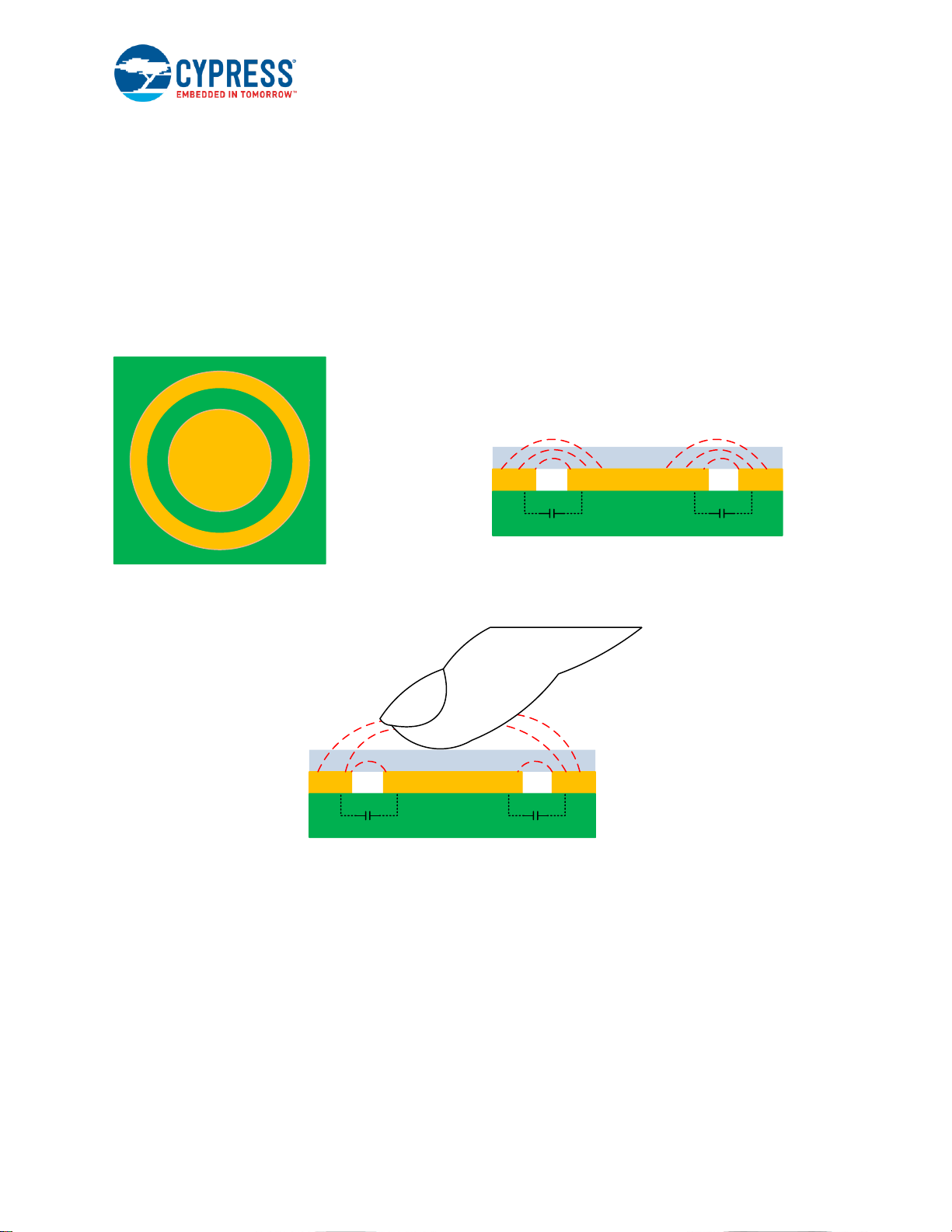
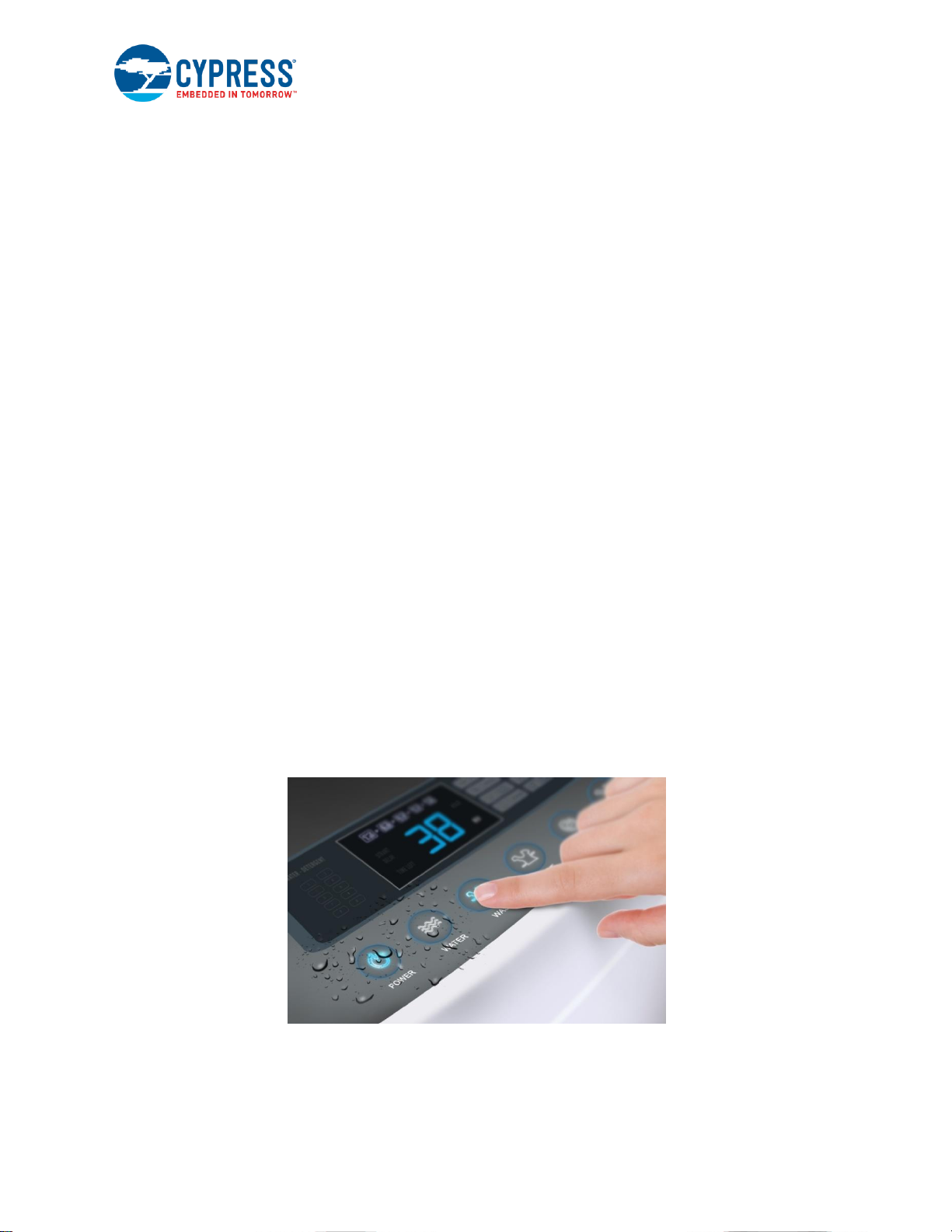
2.8 Liquid Tolerance
CapSense is used in a variety of applications such as home appliances, automotive, and industrial applications. These
applications require robust CapSense operation even in the presence of mist, moisture, water, ice, and humidity
changes. In a CapSense design, false sensing of touch may happen due to the presence of a film of liquid or liquid
droplets on the touch surface. Cypress’s CapSense sensing method can compensate for variation in raw count due to
mist, moisture, water, ice, and humidity changes and provide a robust, reliable, CapSense operation.
Figure 2-31. CapSense-based Touch User Interface in a Washing Machine with Liquid Tolerance
To compensate for changes in raw count due to mist, moisture, and humidity changes, the CapSense sensing method
continuously adjusts the baseline of the sensor to prevent sensor false triggers. To compensate for changes in raw
count due to a liquid droplet or liquid flow, you should implement a Shield Electrode and a Guard Sensor to provide
robust touch sensing, as Figure 2-32 shows. All sensor pins can optionally have a 560-Ω series resistor for improved
noise immunity.
Page 29

CapSense Technology
AN64846 - Getting Started with CapSense® Doc. No. 001-64846 Rev. *X 29
When liquid droplets are present on the touch surface and if the shield electrode is implemented, the CapSense system
can reliably work even in the presence of liquid droplets and report sensor ON/OFF status. When there is a liquid flow
or a liquid pool on the touch surface, the CapSense system detects the liquid by using a guard sensor and disables the
scanning for all other sensors in the system to prevent false triggers. Therefore, when there is a liquid flow or liquid
pool on the touch surface, the CapSense system will not detect a finger touch as long as the liquid is present on the
touch surface.
Figure 2-32. Shield Electrode (SH) and Guard Sensor (GUARD) Connected to CapSense Controller
CS1
CS3
CS2
SH
GUARD
Shield Electrode
Guard Sensor
Button Sensor
560 Ω
560 Ω
560 Ω
560 Ω
CapSense
Controller
2.8.1 Effect of Liquid Droplets and Liquid Stream on CapSense
To understand the effect of a liquid droplet or a liquid stream on a CapSense sensor, consider a CapSense system in
which the hatch fill around the sensor is connected to ground, as Figure 2-33 (a) shows. Surrounding the sensor with
a hatch fill connected to ground improves the noise immunity of the sensor. The parasitic capacitance of sensor is
denoted as CS in Figure 2-33 (b).
Figure 2-33. Typical CapSense System Layout
BTN1
Hatch Fill
Connected to
Ground
Button Sensor
560 Ω
CapSense
Controller
CapSense
Controller
560 Ω
C
S
(a)
(b)
As shown in Figure 2-34, when a liquid droplet falls on the touch surface, due to its conductive nature, it provides a
strong coupling path for the electric field lines to return to ground and therefore adds a capacitance CLD in parallel to
CP. When the sensor is charged and discharged, the capacitance CLD draws some amount of charge from the AMUX
bus because of the nonzero voltage difference across the capacitance CLD. This increases the overall capacitance seen
by the CapSense circuitry and results in an increase in the sensor raw count. In some cases, where the liquid is highly
conductive (salty water or water with high mineral content), the increase in raw count when a liquid droplet falls on the
touch surface might be equal to the increase in raw count due to a finger touch and thus causes false triggers, as Figure
2-35 shows.
Figure 2-34. Capacitance Added by Liquid Droplet when the Hatch Fill Is Connected to Ground
BTN1
Hatch Fill
Connected to
Ground
Button Sensor
560 Ω
CapSense
Controller
CapSense
Controller
560 Ω
C
S
C
LD
Liquid Droplet
CS – Sensor Parasitic Capacitance
Page 30

CapSense Technology
AN64846 - Getting Started with CapSense® Doc. No. 001-64846 Rev. *X 30
C
LD
– Capacitance added by Liquid Droplet
Figure 2-35. Effect of Liquid Droplet when the Hatch Fill Around the Sensor Is Connected to Ground
To compensate the capacitance added by the liquid droplet to the CapSense circuitry, you should drive the hatch fill
surrounding the sensor with the driven-shield signal.
As shown in Figure 2-36, when the hatch fill surrounding the sensor is connected to the driven-shield signal and when
a liquid droplet falls on the touch surface, because the voltage on both the sides of liquid droplet is kept at the same
potential, the capacitance C
LD
added by the liquid droplet is nullified. Because the voltage difference across the
capacitance C
LD
is zero, it will not draw any charge from the AMUX bus and, therefore, the increase in the raw count
when a liquid droplet falls on the sensor will be very small, as Figure 2-37 shows.
Figure 2-36. Capacitance Added by Liquid Droplet when the Hatch Fill around the Sensor Is Connected to Shield
BTN1
Hatch Fill
Connected to
Driven Shield
Button Sensor
560 Ω
CapSense
Controller
CapSense
Controller
560 Ω
C
S
C
SH
C
HG
C
LD
Liquid Droplet
Shield
Sensor Waveform
Driven Shield
Waveform
Shield
CS – Sensor Parasitic Capacitance
CSH – Capacitance between Sensor and Hatch Fill
C
HG
– Capacitance between Hatch Fill and Ground
C
LD
– Capacitance Added by Liquid Droplet
Page 31

CapSense Technology
AN64846 - Getting Started with CapSense® Doc. No. 001-64846 Rev. *X 31
Figure 2-37. Effect of Liquid Droplet when the Hatch Fill Around the Sensor Is Connected to the Driven Shield
2.8.2 Driven-Shield Signal and Shield Electrode
The driven-shield signal is a buffered version of the sensor-switching signal, as Figure 2-38 shows. The driven-shield
signal has the sample amplitude, frequency, and phase as that of the sensor-switching signal. The buffer provides
sufficient current for the driven-shield signal to drive the high parasitic capacitance of the hatch fill on the PCB. When
the hatch fill surrounding the sensor is connected to the driven-shield signal, it is referred as Shield Electrode. As
explained in the Effect of Liquid Droplets and Liquid Stream on CapSense section, because the shield electrode is
driven with a voltage which is the same as the sensor-switching signal, the capacitance added by a liquid droplet when
it falls on the touch surface will be nullified. To achieve the best liquid-tolerance performance, it is required that the
driven shield signal has the same voltage and phase as that of the sensor-switching signal.
Figure 2-38. Driven-Shield Signal
Buffer
Sensor Switching
Signal
Driven Shield
Signal
In-Phase Sensor and
Shield Signal
2.8.3 Guard Sensor
When a continuous liquid stream is applied to the touch interface, the liquid stream adds a large capacitance (CST) to
the CapSense circuitry. This capacitance might be several times larger than CLD. Because of this, the effect of the
shield electrode is completely masked, resulting in the increase in sensor raw count potentially higher than that due to
a finger touch. In such situations, the guard sensor is useful to prevent a false touch-sensing.
A guard sensor is a copper trace that surrounds all the sensors on the PCB, as Figure 2-39 shows. A guard sensor is
similar to a button sensor and is used to detect the presence of liquid stream. When a guard sensor is triggered, the
firmware can disable the scanning of all other sensors in the system to prevent a false touch-sensing. Because the
sensors are not scanned when the guard sensor is triggered, the touch cannot be detected when there is a liquid
stream.
Page 32

CapSense Technology
AN64846 - Getting Started with CapSense® Doc. No. 001-64846 Rev. *X 32
Figure 2-39. Capacitance Measurement with a Liquid Stream
CapSense Controller
CS1
CS3
CS2
SHIELD
GUARD
BTN1 BTN2
BTN3
Shield Electrode
Guard Sensor
Button Sensor
560 Ω
560 Ω
560 Ω
560 Ω
Liquid Stream
2.8.4 Effect of Liquid Properties on the Liquid-Tolerance Performance
In certain applications, the CapSense system has to work reliably in the presence of a variety of liquids such as soap
water, sea water, and water with high mineral content. In such applications, it is recommended that you tune the
CapSense parameters for the sensors by considering the worst-case shift in the raw count due to liquids on the touch
surface. To simulate the worst-case condition, you can prepare a salty water solution by dissolving 40 gm of cooking
salt (NaCl) in 1 liter of water and measure the shift in raw counts when water droplets fall on the sensor.
In applications such as an induction cook-top, there might be chances of hot water spilling on the CapSense touch
surface. To determine the impact of temperature of a liquid droplet on the liquid-tolerance performance, tests were
done with liquid droplets at different temperatures. Experiment results show that the effect of hot liquid droplets is the
same as that of the liquid droplets at room temperature. This is because a hot liquid droplet cools down immediately to
room temperature when it falls on the touch surface.
Figure 2-40. Raw Count Variation versus Water Temperature
To make your design liquid-tolerant, follow these steps:
1. Choose a CapSense controller that supports the liquid tolerance feature. Refer to the CapSense Selector Guide
to select the CapSense controller that supports the liquid tolerance feature.
2. Follow the schematic and layout guidelines explained in the device-specific Design Guide to construct the shield
electrode and guard sensor.
3000
3500
4000
4500
5000
5500
6000
6500
24.6 50 85
Raw Count
Temperature in Degree Celsius
Rawcount_BTN0
Rawcount_BTN1
Rawcount_BTN2
Page 33

CapSense Technology
AN64846 - Getting Started with CapSense® Doc. No. 001-64846 Rev. *X 33
3. Tune the guard sensor (if implemented) such that it is triggered only when there is a liquid stream. In the firmware,
ensure that the sensors are not scanned when the guard sensor is triggered.
Refer to the individual CapSense design guides for detailed procedures of how to tune the CapSense parameters to
achieve liquid tolerance. The application note, AN92239 – Proximity Sensing with CapSense, shows how to implement
a proximity-sensing system with liquid tolerance for PSoC 4 devices.
2.9 Proximity Sensing
Proximity sensing is the process of detecting a nearby object without any physical contact. Proximity sensors use an
electromagnetic field, beam of electromagnetic radiation, or changes in ambient conditions to detect the proximity of a
nearby object. There are various types of proximity sensors such as capacitive, inductive, and magnetic, Hall effect,
optical, and ultrasonic sensors; each has its own advantages and disadvantages. Capacitive proximity sensing has
gained huge popularity because of its low cost, high reliability, low power, sleek aesthetics, and seamless integration
with existing user interfaces. This section presents an introduction to CapSense-based proximity sensing. Refer to
AN92239 – Proximity Sensing with CapSense for the complete proximity design guidelines.
2.9.1 Proximity-Sensing Applications Based on CapSense
Proximity sensing based on CapSense is used in a variety of applications as explained below.
Face detection in mobile phones and tablets: Face detection is a feature in mobile phones that disables the phone’s
touchscreen and dims the brightness of the display when a user answers a phone call, as Figure 2-41 shows. Face
detection prevents false touches when the phone is placed on the ear and optimizes the device’s power consumption.
Using proximity sensing based on CapSense in this application offers advantages over IR proximity sensing because
it does not require cutouts in the overlay material, which reduces the tooling cost and improves the aesthetics of the
end product.
Figure 2-41. Face Detection in Mobile Phones
SAR regulation in tablets and mobile phones: SAR is a measure of the rate at which energy is absorbed by the
human body when exposed to an RF electromagnetic field. Regulatory bodies, such as the Federal Communications
Commission (FCC), require devices to limit the absorption of RF energy by reducing the device’s RF transmit power
when the device is in close proximity to the human body, as Figure 2-42 shows. Proximity sensors based on CapSense
can be used to detect the proximity of the human body and reduce RF power.
Figure 2-42. SAR Regulation in Tablets
Wake-on-approach: This feature activates the system from the sleep or standby mode when an object approaches
the system, as Figure 2-43 shows. Wake-on-approach is also used to control the backlight LEDs when the user
approaches the system. This feature reduces system wakeup time, improves device responsiveness, reduces device
power consumption, and improves aesthetics. It is useful in battery-operated applications such as mice and keyboards.
Figure 2-43. Wake-on-Approach Implemented in a Mouse
Page 34

CapSense Technology
AN64846 - Getting Started with CapSense® Doc. No. 001-64846 Rev. *X 34
Gesture detection: Gesture detection is the technique of interpreting human body movements and providing gesturetype information to the device. Gesture-based user interfaces provide an intuitive way for the user to interact with the
system, improving the user experience. Gesture detection is used in applications such as laptops, tablets, and mobile
phones for controlling the user interface.
Proximity sensors based on CapSense can be used in these applications to detect gestures without any physical
contact between the user and the device. Figure 2-44 shows an example of an implementation of gesture detection in
a laptop where proximity sensors placed near the trackpad are used for the pan movement of the onscreen map.
Figure 2-44. Gesture Detection Implementation in a Laptop
IR replacement: Proximity sensors based on CapSense can replace IR proximity sensors in applications such as
faucets and soap dispensers, as Figure 2-45 shows. Proximity sensing based on CapSense offers the following
advantages over IR proximity sensing:
It is a low-cost solution compared to IR proximity sensing. Proximity sensors based on CapSense can be
constructed using a copper trace on the PCB, whereas IR proximity sensing requires extra IR sensors.
Proximity sensors based on CapSense do not require any cutout in the overlay material to detect proximity sensing,
unlike IR proximity sensors. Therefore, proximity sensing based on CapSense reduces the tooling cost and
improves the aesthetics of the end product.
They consume less power than IR proximity sensors.
They are immune to ambient light, whereas IR-based proximity sensors can have performance issues with varying
ambient light.
Page 35

CapSense Technology
AN64846 - Getting Started with CapSense® Doc. No. 001-64846 Rev. *X 35
Figure 2-45. Proximity Sensing Based on CapSense in a Soap Dispenser
2.9.2 Proximity Sensing with CapSense
The proximity-sensing technique based on CapSense involves measuring the change in capacitance of a proximity
sensor when a target object approaches the sensor. The target object can be a human finger, hand, or any conductive
object. Proximity sensors can be constructed using a conductive (usually copper or indium tin oxide) pad or trace laid
on a nonconductive material like PCB or glass. In essence, a proximity sensor is like any other sensor but designed
with very minimum ground near the sensor and tuned for maximum sensitivity.
For detecting the target object, the Signal-to-Noise Ratio (SNR) should be greater than or equal to 5:1. Therefore, you
can detect the proximity of the target object without error up to a certain distance from the sensor. This distance is
called the proximity-sensing distance. Refer to Proximity Sensing Design to learn the various ways of constructing a
proximity sensor and to learn the various parameters that affect the proximity distance.
2.10 User Interface Feedback
Effective user interface designs include feedback to the user when they are using the capacitive touch sense buttons.
There are various forms of feedback, including visual, audio, and haptic (tactile). Depending on the user interface
design, multiple types of feedback can be used in combination.
2.10.1 Visual Feedback
LEDs and LCDs provide visual feedback.
2.10.1.1 LED-Based Visual Feedback
Visual feedback is widely used in user interfaces. LEDs are used to indicate the status of buttons, sliders, and proximity
sensors. LEDs can implement different effects when the sensor status changes as listed below.
LED ON/OFF – GPOs are used to drive LEDs in either a sourcing (GPO supplies current to the LED) or sinking
(GPO sinks current from the LED) configuration.
LED Brightness Control - For user interfaces that require sophisticated visual effects, a single hardware PWM or
timer can be used to drive the LEDs. By varying the duty cycle of the PWM output, you can adjust the LED
brightness. This enables adjusting your user interface brightness in response to ambient lighting conditions.
LED Fading - By gradually changing the duty cycle between LED states, you can achieve a fading effect. For
example, the LED appears to “fade in” (from OFF to ON) when the duty cycle is increased in a series of small
steps.
LED Breathing - Gradually increasing and decreasing the duty cycle between two levels on a continuous basis
makes the LED appear to “breathe”. LED breathing is useful when a system is in idle or stand-by mode. For
example, a power button can appear to breathe to alert the user that it is active and can be operated.
2.10.1.2 LCD-Based Visual Feedback
LCDs provide visual feedback for CapSense buttons and sliders. The main advantage of using an LCD is that it can
provide more information along with the feedback for each button press event. Depending on the device family,
Page 36

CapSense Technology
AN64846 - Getting Started with CapSense® Doc. No. 001-64846 Rev. *X 36
programmable devices support different types of LCD technologies with pre-built components and user modules which
provide APIs for displaying data with ease.
Character LCD with parallel interface - PSoC devices support interface with the Hitachi HD44780A LCD module.
Figure 2-46 shows the typical connection for using the Hitachi HD44780A LCD module. Refer to the character LCD
component datasheet to learn more.
Figure 2-46. Hitachi Dot Matrix LCD Pin Connections
Character LCD with I2C Interface - PSoC can also control LCDs through I2C with support for the NXP PCF2119x
command format. Figure 2-47 shows the typical circuit diagram for driving an LCD with I2C interface. Refer to the
component datasheet to learn more.
Figure 2-47. Interfacing an LCD with I2C Interface
PSoC LCD Module
VDD
SCL
SDA
Segment LCD Glass - PSoC devices integrate the LCD driver to directly drive a segment LCD glass. Refer to the
CapSense Selector Guide to know the LCD drive capability of different PSoC devices.
2.10.2 Haptic Feedback
Haptic or tactile feedback uses vibration to let you know that the system has detected a finger touch.
Page 37

CapSense Technology
AN64846 - Getting Started with CapSense® Doc. No. 001-64846 Rev. *X 37
Figure 2-48. Cypress Haptics Ecosystem
Different haptic effects are created by varying the duration, frequency, and shape of the vibration profile. Vibrations are
created by an actuator. The key requirements for an actuator are - Response time, Power consumption, Size, Form
factor, Durability, and Vibration strength. Multiple actuator options are available with varying drive requirement. The
four types of actuators are:
Eccentric Rotation Mass (ERM) actuators – These actuators are most cost-effective, have a current requirement
of 130 to 160 mA, and require an external power amplifier for drive. These are not suitable for applications requiring
fast response such as typing.
Linear Resonant Actuators (LRAs) - LRAs are used in many smartphones, require AC input, draw current at around
65 to 70 mA, are relatively faster, but cost more than ERM actuators. LRAs require an external power amplifier for
drive.
Piezo Modules – Piezo modules respond fast, making them suitable for typing applications, but they cost more
than ERM and LRA actuators. Though their instantaneous current draw is more at around 300 mA at 3-V supply,
their average current consumption is not more than the ERM and LRA actuators.
Electro-Active Polymer Actuators (EAPs) – EAPs offer a performance similar to that of the piezo modules but
integrating them into tight spaces is a challenge. They require 800 V for a drive signal.
The CY8C20XX6H CapSense controller integrates Immersion’s TS2000 Haptic effects library for Eccentric Rotating
Motor (ERM) drive control and can generate 14 predefined haptic effects. The Haptics User Module datasheet has
more information about these effects and also provides a code example. To know more about CY8C20XX6H, refer to
the device datasheet.
2.10.3 Audible Feedback
Audible feedback for CapSense buttons is implemented using a buzzer. The pulse-width modulator (PWM) is used to
output the PWM signal required for driving the buzzer as specified in the buzzer datasheet. When a button press event
occurs, the feedback is given by driving the buzzer at a particular intensity level. The circuit diagram for implementing
the buzzer feedback follows.
Page 38

CapSense Technology
AN64846 - Getting Started with CapSense® Doc. No. 001-64846 Rev. *X 38
Figure 2-49. Implementing Audible Feedback for CapSense
Page 39

AN64846 - Getting Started with CapSense® Doc. No. 001-64846 Rev. *X 39
3. Design Considerations
When designing capacitive touch sense technology into your application, it is important to remember that the CapSense
device exists within a larger framework. Careful attention to every level of detail from PCB layout to user interface to
end-use operating environment will enable robust and reliable system performance.
3.1 Overlay Selection
In a CapSense design, overlay material is placed over the sensor pad to protect it from the environment and prevent
direct finger contact.
3.1.1 Overlay Material
In the Self Capacitance section, Equation 1 shows the finger capacitance.
Where:
ε
0
= Free space permittivity
ε
r
= Dielectric constant of overlay
A = Area of finger and sensor pad overlap
D = Overlay thickness
The geometry of a CapSense system is more complex than a parallel plate capacitor. The conductors in the sensor
include the finger and PCB copper. However, like a parallel plate capacitor, CF is directly proportional to εr. High
dielectric constants lead to high sensitivity. Because air has the lowest dielectric constant, any air gaps between the
sensor pad and overlay must be eliminated.
Dielectric constants of some common overlay materials are listed in Table 3-1. Materials with dielectrics between 2.0
and 8.0 are well suited to capacitive sensing applications.
Table 3-1. Dielectric Constants of Common Materials
Material
r
Air
1.0
Formica®
4.6–4.9
Glass (Standard)
7.6–8.0
Glass (Ceramic)
6.0
PET Film (Mylar®)
3.2
Polycarbonate (Lexan®)
2.9–3.0
Acrylic (Plexiglass®)
2.8
ABS
2.4–4.1
Wood Table and Desktop
1.2–2.5
Gypsum (Drywall)
2.5–6.0
Conductive material cannot be used as an overlay because it interferes with the electric field pattern. For this reason,
do not use paints that contain metal particles in the overlay.
Page 40

Design Considerations
AN64846 - Getting Started with CapSense® Doc. No. 001-64846 Rev. *X 40
3.1.2 Overlay Thickness
Sensitivity is inversely proportional to overlay thickness, as illustrated in Figure 3-1.
Figure 3-1. Sensitivity Versus Overlay Thickness
Both signal and noise are affected by the overlay properties. Table 3-2 lists the recommended maximum overlay
thicknesses for PSoC CapSense applications with an acrylic overlay material.
Table 3-2. Maximum Overlay Thickness with an Acrylic Overlay Material
Design Element
Max. Overlay Thickness (mm)
Button
5
Slider
5
Touchpad
0.5
3.1.3 Overlay Adhesives
Overlay materials must have good mechanical contact with the sensing PCB. This is achieved using a nonconductive
adhesive film. This film increases the sensitivity of the system by eliminating any air gaps between overlay and the
sensor pads. 3M™ makes a high-performance acrylic adhesive called 200MP that is widely used in CapSense
applications in the form of adhesive transfer tape (product numbers 467MP and 468MP).
3.2 ESD Protection
Robust ESD tolerance is a natural byproduct of a thoughtful system design. By considering how contact discharge will
occur in your end-product, particularly in your user interface, it is possible to withstand an 18-kV discharge event without
any damage to the CapSense controller.
Table 3-3. Overlay Material Dielectric Strength
Material
Breakdown Voltage
(V/mm)
Min. Overlay Thickness
at 12 kV (mm)
Air
1200–2800
10
Wood – dry
3900
3
Glass – common
7900
1.5
Glass – Borosilicate (Pyrex®)
13,000
0.9
PMMA Plastic (Plexiglass)
13,000
0.9
ABS
16,000
0.8
Polycarbonate (Lexan)
16,000
0.8
Formica
18,000
0.7
FR-4
28,000
0.4
PET Film (Mylar)
280,000
0.04
Polymide film (Kapton®)
290,000
0.04
Page 41

Design Considerations
AN64846 - Getting Started with CapSense® Doc. No. 001-64846 Rev. *X 41
CapSense controller pins can withstand a direct 2-kV event. In most cases, the overlay material provides sufficient ESD
protection for the controller pins. Table 3-3 lists the thickness of various overlay materials required to protect the
CapSense sensors from a 12-kV discharge as specified in IEC 61000-4-2. If the overlay material does not provide
sufficient protection, ESD countermeasures should be applied in the following order: Prevent, Redirect, Clamp.
3.2.1 Preventing ESD Discharge
Preventing the ESD discharge from reaching the CapSense controller is the best countermeasure you can take. Make
certain that all paths on the touch surface have a breakdown voltage greater than any voltage to which the surface may
be exposed. Also, design your system to maintain an appropriate distance between the CapSense controller and
possible sources of ESD. In the example illustrated in Figure 3-2, if L1 and L2 are greater than 10 mm, the system will
withstand 12 kV.
Figure 3-2. ESD Path
Air-Filled Space
PCB
CapSense
Non-Conductive
Material
ESD Event
Mechanical Structure
Exposed
Mounting
Hardware
ESD Event
L2
L1
If it is not possible to maintain adequate distance, place a protective layer of a high-breakdown voltage material between
the ESD source and CapSense controller. One layer of 5 mil-thick Kapton tape will withstand 18 kV. See Table 3-3 for
other material dielectric strengths.
3.2.2 Redirect
If your product is densely packed, it may not be possible to prevent the discharge event. In this case, you can protect
the CapSense controller by controlling where the discharge occurs. This can be achieved through a combination of
PCB layout, mechanical layout of the system, and conductive tape or other shielding material. A standard practice is to
place a guard ring on the perimeter of the circuit board. The guard ring should connect to chassis ground.
Figure 3-3. Guard Ring
CapSense
Controller
Ground With Conductive
Material on the Perimeter to
Direct Discharge Away From
CapSense Controller
As recommended in PCB Layout Guidelines, providing a hatched ground plane around the button or slider sensor can
also redirect the ESD event away from the sensor and CapSense controller.
Page 42

Design Considerations
AN64846 - Getting Started with CapSense® Doc. No. 001-64846 Rev. *X 42
3.2.3 Clamp
Because CapSense sensors are placed in close proximity to the touch surface, it may not be practical to redirect the
discharge path. Including series resistors or special purpose ESD protection devices may be appropriate. Adding a
series resistor on the vulnerable traces is a cost-effective protection method. This technique works by splitting the
dissipation between the resistor and the controller. The recommended series resistance added to the CapSense inputs
is 560 ohms. More details are available in the Series Resistor section.
Figure 3-4. ESD Protection Using a Series Resistor
A more effective method is to provide special-purpose ESD protection devices on the vulnerable traces. ESD protection
devices for CapSense need to be low capacitance. Table 3-4 lists devices recommended for use with CapSense
controllers.
Table 3-4. ESD Protection Devices
ESD Protection Device
Input
Capacitance
Leakage
Current
Contact Discharge
Maximum Limit
Air Discharge
Maximum
Limit
Manufacturer
Part Number
Littelfuse
SP723
5 pF
2 nA
8 kV
15 kV
Vishay
VBUS05L1-DD1
0.3 pF
0.1 µA <
+/-15 kV
+/-16 kV
NXP
NUP1301
0.75 pF
30 nA
8 kV
15 kV
3.3 Electromagnetic Compatibility (EMC) Considerations
EMC is related to the generation, transmission, and reception of electromagnetic energy that can upset the working of
an electronic system. The source (emitter) produces the emission and a transfer or coupling path transfers the emission
energy to a receptor, where it is processed, resulting in either desired or undesired behavior. Electronic devices are
required to comply with specific limits for emitted energy and susceptibility to external events. Several regulatory bodies
worldwide set regional regulations to help ensure that electronic devices do not interfere with each other.
CMOS analog and digital circuits have very high-input impedance. As a result, they are sensitive to external electric
fields. Therefore, you should take adequate precautions to ensure their proper operation in the presence of radiated
and conducted noise.
3.3.1 Radiated Interference and Emissions
Radiated electrical energy can influence system measurements and potentially influence the operation of the CapSense
processor core. The interference enters the CapSense chip at the PCB level through the sensor traces and other digital
and analog inputs. While CapSense offers an intuitive and robust interface that increases product reliability by
eliminating mechanical parts, it can also contribute to electromagnetic compatibility (EMC) issues in the form of radiated
emissions (RE).
Use the following techniques to minimize radiated interference and emissions.
Page 43

Design Considerations
AN64846 - Getting Started with CapSense® Doc. No. 001-64846 Rev. *X 43
3.3.1.1 General EMI/EMC Guidelines
3.3.1.1.1 Ground Plane
In general, a proper ground plane on the PCB reduces both RF emissions and interference. However, solid grounds
near CapSense sensors or traces connecting these sensors to the PSoC pins increase the parasitic capacitance of the
sensors. It is thus recommended that you use hatched ground planes surrounding the sensor and on the bottom layer
of the PCB, below the sensors, as explained in the Ground Plane section. A solid ground may be used below the device
and other circuitry on the PCB, which is far from CapSense sensors and traces. A solid ground flood is not
recommended within 10 mm of CapSense sensors or traces. Multiple-layer boards should be the preferred choice. If
you are using a board with four layers or more, you can provide a complete layer for ground that will further help to
reduce emissions as it reduces the ground bounce significantly.
3.3.1.1.2 Series Resistor
Every CapSense controller pin has some parasitic capacitance (CP) associated with it. Adding an external resistor
forms a low-pass RC filter that can dampen the RF noise amplitude coupled with the pin. This resistance also forms a
low-pass filter with the parasitic capacitance of the trace connected to the pin (for example, sensor trace and sensor
pad as shown in Figure 3-5) that can significantly reduce RF emissions. Thus, series resistors help in eliminating higher-
order harmonics and attenuating the RF interference and emission.
Figure 3-5. RC Filter
CapSense
Controller
CapSense
Sensor
External Series
Resistor
Pins
Capacitance
Series resistors should be placed close to the PSoC pins so that the radiated noise picked by the traces gets filtered at
the input of the PSoC device. Thus, it is recommended that you place series resistors within 10 mm of the PSoC pins.
3.3.1.1.2.1 CapSense Input Lines The sensor must be fully charged and discharged during each switching cycle for proper operation of CapSense. The
charge and discharge paths of the sensor capacitor include series resistances that slow down the charging / discharging
process. Figure 3-6 shows an equivalent circuit and resulting waveforms. Adding a resistance changes the time
constant of the switched-capacitor circuit that converts CP into an equivalent resistor. If the series resistance value is
set high, the slower time constant of the switching circuit suppresses the emission but limits the amount of charge that
it can transfer. Thus the sensors may not get charged and discharged completely. This lowers the signal level, which
in turn lowers the SNR. Smaller values are better, but are less effective at blocking RF emissions and interference.
The recommended series resistance for CapSense input lines on general copper PCBs is 560 Ω. An ITO panel already
provides a high resistance; one may not have too much flexibility in the value selection (range 100 Ω –1 kΩ). Series
resistors are generally used in the range of 560 Ω–4.7 kΩ for EMC purpose. The actual maximum value of the series
resistor that can be used varies from device to device. This depends on multiple factors such as the resistance of the
GPIO used as sensor, the switching frequency used to scan sensors, and the SNR required.
Page 44

Design Considerations
AN64846 - Getting Started with CapSense® Doc. No. 001-64846 Rev. *X 44
Figure 3-6: Equivalent Circuit and Waveforms
V
SW
V
S
V
DDD
V
REF
t
t
R
S
C
S
V
SW
switching
clock
V
S
5 R
S
C
S
T
SW
>= 10 R
S
C
S
5 R
S
C
S
V
DDD
V
REF
RS is the sum of the GPIO resistance and the external series resistance. CS is the maximum capacitance of the sensor.
For a given switching frequency, you must select the series-resistor value such that the sensor capacitor is charged
and discharged fully. On the other hand, for a given series resistor, you must choose the switching frequency value
such that the sensor capacitor is charged and discharged fully. Lowering the switching frequency lowers the SNR if you
are unable to modify other CapSense parameters. Therefore, it is a tradeoff between the series resistor value and the
switching frequency to achieve the desired performance.
The rule of thumb is to allow a period of 5RSCS for charging and discharging cycles. Equations for the minimum time
period and maximum frequency are:
3.3.1.1.2.2 Digital Communication Lines Communication lines, such as I2C and SPI, also benefit from series resistance and 330 Ω is recommended for
communication lines. Communication lines have long traces that act as antennae, similar to CapSense traces. The
recommended pull-up resistor value for communication lines is 4.7 kΩ. So, if more than 330 Ω is placed in series on
these lines, the voltage levels (VIL and VIH) fall out of the specifications with the worst-case combination of supply
voltages between systems and the input impedance of the receiver. 330 Ω will not affect the I2C operation because the
VIL level still remains within the I2C specification limit of 0.3 VDD when the PSoC device outputs a LOW.
Figure 3-7: Series Resistors on Communication Lines
CapSense
Controller
Vdd
Vdd
SCL
SDA
4.7K Ohm
4.7K Ohm
330 Ohm
330 Ohm
Page 45

Design Considerations
AN64846 - Getting Started with CapSense® Doc. No. 001-64846 Rev. *X 45
3.3.1.1.3 Trace Length
Long traces can pick up more noise than short traces. Long traces also add to CP. Minimize trace length whenever
possible.
3.3.1.1.4 Current Loop Area
Another important layout consideration is to minimize the return path for current. A ground plane can lower the overall
ground impedance, thus reducing the high-frequency ground bounce. Ensure good GND return paths for each sensor
line. This is important as the current flows in loops. Unless there is a proper return path for high-frequency signals, the
return current will flow through a longer return path forming a larger loop; this can cause signal issues due to mutual
inductance. Thus, it leads to increased emissions and interference.
When a device package contains high-frequency current loops, energy can also be coupled out of the device through
a magnetic field. It is possible for the magnetic flux to form a current loop in the device to link to the circuit loops outside
the device. This mutual inductance can produce an unwanted voltage in the external loop. Likewise, an external
magnetic flux can induce an unwanted voltage across an interior circuit loop. Magnetic field coupling can be minimized
by keeping the power and signal loop areas as small as possible. Stitch all the grounds with as many vias as possible.
This will reduce the overall ground impedance. High-frequency traces, such as those used for clock and oscillator
circuits, should be contained by two ground lines. This will ensure that there is no coupling, which results in crosstalk.
Use separate ground plane and power planes wherever possible.
Figure 3-8 shows an example of an improper grounding scheme. The layout greatly improves by reducing the loop
area.
Figure 3-8. Improper Ground Scheme and Ground Loop
CapSense
Controller
On-Board Driver
Circuits
External Circiuts
1) Decoupling Loop Inductance and
Switching Currents Combine to Create an
AC Voltage on the Local Ground
2) Each Output (and Input) Drives the AC Voltage
Out Onto the PCB. Each Signal Will Have a Loop
Area Associated With It
3) Cables Magnify the Problem as Loop Areas
Are Proportional to Cable Length
In Figure 3-9, two sensors are surrounded by a ground plane that is connected to a CapSense controller ground, while
a third sensor is surrounded by ground. The third sensor is connected to the other ground plane through the long traces
of other circuitry, which creates a large current loop. With this layout, the third sensor may be more susceptible to
radiated noise and have increased emissions. These two sections of ground are in the same location on the schematic,
so they can potentially be one connected area with a better layout.
Page 46

Design Considerations
AN64846 - Getting Started with CapSense® Doc. No. 001-64846 Rev. *X 46
Figure 3-9. Improper Current Loop Layout
CapSense
Sensor
CapSense
mC
Ground Fill
#1
Ground Fill
#2
Isolated
Other
Circuitry
Path to Sensor
Pad
Return
Path
PCB
Figure 3-10 illustrates the proper layout for the previous example. The loop area is reduced by connecting the two
grounded areas.
Figure 3-10. Proper Current Loop Layout
CapSense
Sensor
CapSense
mC
Ground Fill
Connected
Path to Sensor
Pad
Return Path
PCB
Other
Circuitry
3.3.1.1.5 Frequency Hopping
Frequency hopping is a method of spreading the input or operating frequency over a narrow band of frequencies. This
method helps to reduce the peaks and spread out the emissions as well as the interference over a range of frequencies
as shown in Figure 3-11. The following are the methods of frequency hopping in PSoC:
Page 47

Design Considerations
AN64846 - Getting Started with CapSense® Doc. No. 001-64846 Rev. *X 47
Figure 3-11. Frequency Hopping
IMO dithering across sensor scans: IMO dithering or trimming can be done across different sensors. For
example, the IMO frequency is swept over a range from 24 MHz to 22 MHz when the base IMO frequency is
24 MHz. A sensor is scanned at one frequency always. Different sensors are scanned at different frequencies.
This reduces the peaks by spreading the emissions.
IMO dithering within each scan: IMO dithering can be done within each scan as well. When a sensor is being
scanned, the IMO frequency is swept over a range from 24 MHz to 22 MHz. Thus, this method avoids a sensor
being scanned at one frequency. This reduces the peaks by spreading the emissions. This also improves the
immunity to RF interference.
Spread Spectrum Clock (SSC): PSoC can also work using an external clock. Using a spread spectrum clock will
help in spreading out the emissions over a wider range of frequencies, similar to IMO dithering. PSoC1 allows only
port P1[4] to be used to supply the external clock. In this case, pin P1[4] drive mode must be set to HI-Z digital.
This increases the immunity to RF interference and spreads the emissions.
Pseudo random sequencer (PRS): A PRS is used instead of a fixed clock-source to attenuate the emitted noise
on CapSense pins by reducing the amount of EMI created by a fixed frequency-source and to increase the EMI
immunity from other sources and their harmonics. This increases the immunity to RF interference and spreads the
emissions.
3.3.1.2 Radiated Immunity
3.3.1.2.1 RF Source Location
When systems, such as computer monitors or digital photo frames, are designed with CapSense devices, make sure
you prevent noise from LCD inverters and switched-mode power supplies (SMPS) from upsetting the CapSense
system. A simple technique to minimize this kind of interaction is to partition the system with noise sources from
CapSense inputs, as demonstrated in Figure 3-12. Due to the practical limitations of product size, the noise source and
the CapSense circuitry may only be separated by a few inches. This small separation can provide the extra margin
required for good sensor performance, compared to the case with close proximity between noise source and CapSense.
Page 48

Design Considerations
AN64846 - Getting Started with CapSense® Doc. No. 001-64846 Rev. *X 48
Figure 3-12. Separating Noise Sources
Computer monitor
SMPS/LCD Inverter
CapSense interface
Computer monitor
SMPS/LCD Inverter
CapSense interface
Not Recommended Recommended
3.3.1.2.2 EMC Feature
CapSense User Modules and components with the EMC feature implement IMO dithering to scan each sensor. Each
sensor is scanned at two or three different frequencies depending on the immunity level chosen for each sample for
raw count. Use this option to improve the immunity against RF interference.
Figure 3-13. Immunity Level Selection
3.3.1.3 Radiated Emissions
3.3.1.3.1 Operating Voltage
For devices in which sensors switch between an operating voltage and a reference voltage, such as CY8C21x34,
reducing the operating voltage helps to reduce emissions to a great extent. This is because the amplitude of the
switching signal at any pin is dependent on the device’s operating voltage and the emissions are directly proportional
to voltage levels at which the switching happens. Figure 3-14 shows the impact of operating voltage on radiated
emissions.
Figure 3-14. Impact of Operating Voltage on Emissions
50
0
10
20
30
40
-10
150k 1M600k
300k 7M4M10M2M 20M
30M
Frequency in Hz
Level in dBµV/m
5V
3.3V
Page 49

Design Considerations
AN64846 - Getting Started with CapSense® Doc. No. 001-64846 Rev. *X 49
3.3.1.3.2 System Oscillator Frequency (IMO)
Lowering the system clock will significantly lower radiated emissions. However, lowering the system clock impacts the
performance of your system because a low IMO can take more time to scan the sensors and perform the processing.
Therefore, lower the system frequency depending on your application.
3.3.1.3.3 Sensor Switching Frequency
The CapSense sensing methods use a switched-capacitor front end to interact with sensors. Selecting a low frequency
for the switched-capacitor clock helps you to reduce the radiated emissions from the CapSense sensors. Figure 3-15
shows the impact of the sensor-switching frequency.
Figure 3-15. Impact of Switching Frequency
Page 50

Design Considerations
AN64846 - Getting Started with CapSense® Doc. No. 001-64846 Rev. *X 50
3.3.1.3.4 Slew Rate Control
Figure 3-16 shows the impact of rise/fall time of a square wave on radiated emissions. Note that slowing the transitions
introduces the cutoff point and damps the radiated-energy level. Internal clock signals of the CapSense controller are
slew-controlled to reduce the radiated emission.
Figure 3-16. Impact of Slew Rate on Emissions
T
t
ON
A
Amplitude
Frequency
At
ON
/T
0 dB/decade
-20 dB/decade
1/(πt
ON
)
t
ON
t
r
t
f
A
A/2
T
Amplitude
Frequency
At
ON
/T
0 dB/decade
-20 dB/decade
1/(πt
ON
) 1/(πt
r
)
-40 dB/decade
0
3.3.1.3.5 Sensor Scan time
The scan time of sensors impacts radiated emissions. Figure 3-17 shows the impact of the sensor-scan time on radiated
emissions. An increase in the sensor-scan time results in increased emissions. Table 3-5 shows the parameter settings
and associated sensor scan times.
Table 3-5. Sensor Scan time
Parameter
Value
Scan resolution
8 bits
10 bits
Individual sensor scan time
0.021 ms
0.085 ms
Total scan time for five buttons
0.105 ms
0.425 ms
Page 51

Design Considerations
AN64846 - Getting Started with CapSense® Doc. No. 001-64846 Rev. *X 51
Figure 3-17. Effect of Scan Time
3.3.1.3.6 Shield Signal
The shield signal is driven on the hatch fill to reduce the parasitic capacitance of sensors for liquid tolerance and for
proximity sensing. See the Shield Electrode and Guard Sensor section for more details. The shield signal is a replica
of the sensor signal. The shield signal further increases radiated emissions as it is a high-frequency switching signal
and is driven on a spread-out hatch fill. Figure 3-18 shows the emissions with and without the driven-shield signal:
Figure 3-18. Impact of Shield on Emissions
Page 52

Design Considerations
AN64846 - Getting Started with CapSense® Doc. No. 001-64846 Rev. *X 52
You can reduce emissions by the following techniques:
1. Reduce the size of the shield hatch fill to have a maximum of 10 mm from the sensors. Refer to the Shield Electrode
and Guard Sensor section for more details.
2. Drive the shield signal only when required. The shield must be driven only when sensors are scanned, and only
when the sensors that need shield protection are scanned.
3. Limit the placement of the shield to selected sensors only. Do not spread the shield around sensors that do not
need shield protection.
4. Slow the edges of the shield waveform by one of the following means:
a. Add a capacitor filter between the shield electrode port pin and ground
b. In most of the PSoC 1 CapSense devices, the slew rate of the shield signal can also be controlled by
changing the drive mode of the shield pin from Strong to Strong Slow as shown in Figure 3-19:
Figure 3-19. Drive Mode Selection for Shield
Add a passive low-pass filter (LPF) to the shield signal by putting a series resistor to the shield pin. An inherent LPF is
formed by the resistance of the electrode material and the parasitic capacitance of the electrode. Therefore, adding a
series resistor increases the RC of the filter and helps to improve emissions to a great extent because the RC filter
formed will eliminate higher-order harmonics of these frequencies.
Note: Filtering the shield too much can cause a phase difference between the driven-shield signal and the sensorswitching signal. Ensure that the shield electrode gets charged and discharged completely when you add filters. Refer
to the CapSense Input Lines section for charge and discharge waveforms, and to see how to choose the right value for
series resistors.
3.3.1.3.7 Inactive Sensor Termination
Connect inactive sensors to ground to reduce emissions instead of the shield unless it is a stringent requirement to
connect them to the shield. Figure 3-20 shows the impact of different inactive-sensor terminations on radiated
emissions.
Figure 3-20. Effect of Inactive Sensor Termination
Page 53

Design Considerations
AN64846 - Getting Started with CapSense® Doc. No. 001-64846 Rev. *X 53
For CapSense applications, it is very important to have a clean power supply for CapSense devices to reduce problems
related to radiated interference and emissions. Guidelines to filter the noise at the power supply of CapSense devices
are given in the following section. It is recommended that you incorporate these guidelines to handle any EMC/EMI
issues.
3.3.2 Conducted Immunity and Emissions
The noise current generated by high-frequency switching circuits entering the system through the power and
communication lines is called conducted noise.
3.3.2.1 Board-Level Solutions
Proper use of decoupling capacitors as recommended by the datasheet can limit the problem with conducted emissions.
For detailed information on general decoupling capacitors, refer to the section 3.8.13 . For unregulated power supplies,
use a large electrolytic capacitor (typically 10 µF –100 µF), no more than one inch away from the chip. This capacitor
acts as a reservoir of charge to supply the instantaneous charge requirements of the circuits locally so that the charge
need not come through the inductance of the power trace.
For further protection, a passive filter can be used. Passive filter effectively limits not just the conducted noise emitted
but also the noise entering the system. Thus, it improves the conducted noise immunity of the system.
A pi-filter is a simple bidirectional low-pass filter. The two main types of pi-filters are the series inductor and the series
resistor. The series inductor pi-filter has two shunt capacitors and one series inductor configured similar to the Greek
letter π, as shown in Figure 3-21. The noise is filtered by all three elements (L1, C1, and C2) in both directions. The
bidirectional nature of the filter is important. Not only does it prevent the supply noise from affecting sensitive parts, it
can also prevent the switching noise of the part from coupling back to the power planes.
Figure 3-21. Series Inductor Pi-Filter
The values of the components are selected based on the frequency that needs to be attenuated.
3.3.2.2 Power Supply Solutions
The following guidelines help you to prevent conducted noise from entering your CapSense design:
Provide GND and VDD planes that reduce current loops.
If the CapSense controller PCB is connected to the power supply by a cable, minimize the cable length and
consider using a shielded cable.
To reduce high-frequency noise, place a ferrite bead around the power supply or communication lines.
- Localizes the noise in the system.
- Keeps external high frequency noise away from the IC.
- Keeps internally generated noise from propagating to the rest of the system
For more information on design considerations for EMC, refer to the following documents:
Top 10 EMC Design Considerations
AN2155 - PSoC EMI Design Considerations
AN80994 - Design Considerations for EFT Immunity
Page 54

Design Considerations
AN64846 - Getting Started with CapSense® Doc. No. 001-64846 Rev. *X 54
3.4 Software Filtering
Software filters are one of the techniques of dealing with high levels of system noise. Table 3-6 lists the types of filters
that are useful for CapSense.
Table 3-6. CapSense Filter Types
Type
Description
Application
Average
Finite impulse response filter (no feedback) with
equally weighted coefficients
Periodic noise from power supplies
IIR
Infinite impulse response filter (feedback) with a
step response similar to an RC filter
High frequency white noise (1/f noise)
Median
Nonlinear filter that computes median input value
from a buffer of size N
Noise spikes from motors and switching power supplies
Jitter
Nonlinear filter that limits current input based on
previous input
Noise from thick overlay (SNR < 5:1), especially useful for
slider centroid data
Event-Based
Nonlinear filter that causes a predefined response
to a pattern observed in the sensor data
Commonly used to block generation or posting of
nonexistent events
Rule-Based
Nonlinear filter that causes a predefined response
to a pattern observed in the sensor data
Commonly used during normal operation of the touch
surface to respond to special scenarios such as
accidental multi-button selection
3.4.1 Average Filter
An average filter is a finite impulse response (FIR) filter with equal-weighted coefficients. The average filters work well
with periodic noise that is attenuated by spacing the samples out over one noise cycle. Sample spacing is not critical.
For example, power line noise can be anywhere from 50 Hz to 60 Hz. Without adjusting the sampling rate, the average
filter works well for 50-Hz and 60-Hz noise. Figure 3-22 shows a sample rate that is synchronized with a simple periodic
waveform. There is no feedback path in this filter.
Figure 3-22. Synchronized Sample Rate
The general equation for an average filter is:
Equation 15
Figure 3-23 and Figure 3-24 illustrate the results of using an average filter on real CapSense data using the
16-sample filter equation:
Equation 16
Page 55

Design Considerations
AN64846 - Getting Started with CapSense® Doc. No. 001-64846 Rev. *X 55
Figure 3-23. Average Filter Noise (16 Samples)
Unfiltered
Filtered
Unfiltered
Filtered
Figure 3-24. Average Filter Finger Touch (16 Samples)
The previous examples are representative of power supply noise. The filter works well in this example because the
period of the noise is close to the length of the filter (N = 16). For more information about how to implement an average
filter, see the code example CSA Software Filters with EzI2Cs Slave on CY8C20XX6.
Page 56

Design Considerations
AN64846 - Getting Started with CapSense® Doc. No. 001-64846 Rev. *X 56
3.4.2 IIR Filter
Infinite impulse response filters (IIR) produce a step response similar to RC filters. IIR filters attenuate high-frequency
noise components and pass lower frequency signals, such as finger touch-response waveforms.
Figure 3-25. IIR Filter Step Response
The general equation for a first-order IIR filter is:
Equation 17
Figure 3-26 and Figure 3-27 illustrate the results of a first-order IIR filter on real CapSense data using the filter equation
with k = 16:
Equation 18
Figure 3-26. IIR Filter Noise
Page 57

Design Considerations
AN64846 - Getting Started with CapSense® Doc. No. 001-64846 Rev. *X 57
Figure 3-27. IIR Filter Finger Touch
Unfiltered
Filtered
Unfiltered
Filtered
For more information about how to implement an IIR filter, see the code example CSA Software Filters with EzI2Cs
Slave on CY8C20XX6.
3.4.3 Median Filter
Median filters eliminate noise spikes most commonly associated with motors and switching power supplies. In a median
filter, a buffer of size N stores the N most recent samples of the input. The median is then computed using a two-step
process. First, the buffer values are sorted from smallest to largest; then, the middle value is selected from the ordered
list. The buffer is scanned for the median with each update of the buffer. This is a nonlinear filter. The general equation
for a median filter is:
Equation 19
Figure 3-28 and Figure 3-29 show the results of a median filter on real CapSense data using the general filter equation
with N = 16.
Equation 20
Figure 3-28. Median Filter Noise Spike
Page 58

Design Considerations
AN64846 - Getting Started with CapSense® Doc. No. 001-64846 Rev. *X 58
Figure 3-29. Median Filter (16-Sample) Finger Touch
For more information about how to implement a median filter, see the code example CSA Software Filters with EzI2Cs
Slave on CY8C20XX6.
3.4.4 Jitter Filter
3.4.4.1 Jitter Filter for Noisy Slider Data
The centroid function is used to estimate finger position on a slider. When the signal level is low, usually because of
thick overlay on the slider, the estimate of finger position will appear to shake and jitter even when the finger is held at
a fixed position. This jitter noise can be removed using a jitter filter. To do this, the previous input is stored in a buffer.
The current input is compared to the previous output. If the difference is greater than ±1, the output is changed by ±1
(matching sign), as shown in Equation 21. This is a nonlinear filter.
Equation 21
Figure 3-30 shows the results of applying a jitter filter applied to noisy centroid data.
Figure 3-30. Jitter Filter Applied to Noisy Centroid Data
Unfiltered
Filtered
Page 59

Design Considerations
AN64846 - Getting Started with CapSense® Doc. No. 001-64846 Rev. *X 59
3.4.4.2 Jitter Filter for Raw Counts
Although the jitter filter is intended for use with noisy slider data, it is also used with noisy buttons. If the change in the
current input exceeds a set threshold level, the output is reverted to the previous input plus or minus the threshold
amount. The output does not change if the current input changes by less than the threshold amount. The general
equation for a jitter filter applied to buttons is:
Equation 22
Figure 3-31 and Figure 3-32 show the result of using a jitter filter on real button data with a large component of periodic
noise.
Figure 3-31. Jitter Filter for Button Noise
Figure 3-32. Jitter Filter for Button Finger Touch
Unfiltered
Filtered
Unfiltered
Filtered
For more information about how to implement a jitter filter, see the code example CSA Software Filters with EzI2Cs
Slave on CY8C20XX6.
Page 60

Design Considerations
AN64846 - Getting Started with CapSense® Doc. No. 001-64846 Rev. *X 60
3.4.5 Event-Based Filters
Event-based filters involve a special filtering method, where a pattern observed in the sensor data causes a predefined
response in the CapSense system. The pattern in the data is triggered by an event, such as a handheld product placed
into a pocket, or the power supply voltage (VDD) dropping suddenly in a camera phone when the camera flash circuit is
being charged. Following are the common responses used with an event-based filter:
To block the CapSense data transmission until the pattern returns to normal
To reset the level of the baseline reference defined in SNR
To drop or ignore the sample of data when the event occurred
An example for an event-based filter is dropping the sample or resampling of the data when the interrupt occurred. I2C
is one of the common communication protocols used in CapSense applications. Because I2C interrupts are
asynchronous in nature, they may occur when the sensors are being scanned. Interrupts that occur during the scan
may increase the noise and, therefore, decrease the SNR. In such cases, you may implement an event-based filter,
such as ignoring the raw count sample corresponding to that scan when interrupts occurred and rescanning.
3.4.6 Rule-Based Filters
Rule-based filters are another special filtering method, where a pattern observed in the sensor data causes a rulebased response in the CapSense system. Unlike the event-based filter, the rule-based filter acts on patterns in the
sensor data that are encountered during normal operation of the touch surface. The rule-based filter takes into account
special scenarios on how sensors are used.
For example, with a set of radio channel selection buttons, two buttons can be touched accidentally, but only one should
be selected. The rule-based filter sorts out these kind of situations in a predefined way. Another example is having a
virtual sensor in CapSense applications. The virtual sensor is not expected to be triggered during normal operation of
the sensors, but it may occur in unexpected scenarios such as presence of water (for example, the guard sensor) or
when the system is subjected to RF noise. Therefore, when the virtual sensor is triggered, all the actual sensors are
turned off so that there is no unintended triggering of the actual sensors.
3.5 Power Consumption
Minimizing power consumption is an important design goal. For many CapSense systems, extending battery life is
critical to the success of the product. In systems that do not use batteries, power consumption still plays a role in
optimizing power supply designs to reduce costs and PCB area.
3.5.1 Active and Sleep Current
Active current is the current consumed by the device when all the selected analog and digital blocks are enabled and
the CPU is running. In typical applications, the CapSense controller does not need to be in the Active state all the time.
The device can be put into the Sleep state to stop the CPU and the major blocks of the device. Current consumed by
the device in Sleep state is called sleep current. Sleep current is much lower than the active current.
3.5.2 Average Current
In typical applications, sleep state can be invoked periodically to reduce power consumption. This means that during a
preset time period, the CapSense controller wakes up from sleep state, performs all necessary operations in the active
state (scan all sensors, update all baselines, check if any sensor is in the TOUCH state, and so on), and then returns
to sleep state. The resulting instantaneous current graph is shown in Figure 3-33.
Page 61

Design Considerations
AN64846 - Getting Started with CapSense® Doc. No. 001-64846 Rev. *X 61
Figure 3-33. Instantaneous Current
I(t)
t
I
Act
I
Slp
t
Act
t
Slp
T
Where:
I(t) = Instantaneous current
I
Act
= Active current
I
Slp
= Sleep current
t
Act
= Active time
t
Slp
= Sleep time
T = Time period of a cycle
The average current consumed by the device over a long period can be calculated by using the following equation.
Equation 23
The average power consumed by the device can be calculated as follows:
Equation 24
3.5.3 Response Time Versus Power Consumption
As illustrated in Equation 24, the average power consumption can be reduced by decreasing I
AVE
or VDD. I
AVE
may be
decreased by increasing sleep time. Increasing sleep time to a very high value leads to poor response time of the
CapSense button. Because of this tradeoff between response time and power consumption, the application developer
must carefully select the sleep time based on system requirements.
In any application, if both power consumption and response time are important parameters to be considered, then, an
optimized method can be used that incorporates both continuous-scan and sleep-scan modes. In this method, the
device spends most of its time in sleep-scan mode where it scans the sensors and goes to sleep periodically as
explained in the previous section and thereby consuming less power. When you touch a sensor to operate the system,
the device jumps to continuous-scan mode where the sensors are scanned continuously without invoking sleep and
thereby giving very good response time. The device remains in continuous-scan mode for a specified
time-out period. If you do not operate any sensor within this time-out period, the device returns to the sleep-scan mode.
Page 62

Design Considerations
AN64846 - Getting Started with CapSense® Doc. No. 001-64846 Rev. *X 62
3.6 Proximity Sensing Design
This section presents the steps involved in implementing a proximity sensor and the various factors that affect the
proximity distance. For the detailed design guidelines, refer to AN92239 – Proximity Sensing with CapSense.
3.6.1 Implementing Proximity Sensing with CapSense
Figure 3-34 shows the steps for designing a proximity-sensing system based on CapSense.
1. Understand proximity sensing: The Proximity Sensing section in this design guide explains how proximity
sensing, based on CapSense, works and describes the parameters that affect proximity-sensing distance.
2. Evaluate how proximity sensing works: Use Cypress’s CY8CKIT-024 – CapSense Proximity Shield.
3. Specify the proximity-sensing requirements: After evaluating the proximity sensor performance, specify the
proximity-sensing requirements such as the required proximity-sensing distance, area available on the PCB for
sensor construction, system power consumption requirements, and EMI/ESD performance. These requirements
help you to select the right CapSense device and design the sensor layout.
4. Select the right CapSense device: After the requirements are finalized, refer to the CapSense Selector Guide
chapter to select the right CapSense device based on the required proximity-sensing distance.
5. Design the schematic and layout: After selecting the CapSense device, design the schematic and layout. Follow
the guidelines mentioned in the Pin Assignments section to design the schematic. You should also refer to the
device datasheet and device-specific CapSense Design Guides for details on the schematic design. For proximity-
sensor layout guidelines such as proximity-sensor type and size, refer to the section Proximity Sensor Design and
Factors Affecting Proximity Distance.
6. Build the prototype: After the schematic and layout design is completed, build the prototype of the design to
check if the design meets the performance requirements.
7. Tune: Tune the prototype board to achieve the required performance. See the AN92239 – Proximity Sensing with
CapSense and device-specific CapSense Design Guides.
After tuning the sensor, check if the proximity sensor performance meets the requirements. If the requirements are
met, proceed to step 11; otherwise continue with Step 8.
8. Redesign if necessary: If the proximity sensor does not provide the required performance after you have set the
optimum parameters, increase the sensor size or reduce the noise in the system by shielding the sensor from
noise sources and continue with Step 9.
9. Retune: After redesigning the proximity sensor, retune the sensor and check if the sensor performance meets the
requirements. If the requirements are met, proceed to Step 11; otherwise continue with Step 10.
10. Revisit the design or requirements: If the proximity sensor does not meet the required performance even after
you have changed the sensor dimensions to the maximum possible value and tuned it with the optimum
parameters, revisit the requirements.
If you are not able to achieve the required proximity-sensing distance, select a device that has a better proximity
performance than the current device.
If you are not able to achieve the required proximity-sensing distance even with the best device, you need to
change the proximity sensor requirements, such as the area available for the sensor or the required proximitysensing distance, and repeat the procedure from Step 1.
11. Proceed to mass production: If the proximity sensor meets the required performance, you can proceed to mass
production.
Page 63

Design Considerations
AN64846 - Getting Started with CapSense® Doc. No. 001-64846 Rev. *X 63
Figure 3-34. CapSense-based Proximity Sensing Design
Start
Evaluate the Proximity
Sensing Using a Kit
Understand Basics of
Proximity Sensing
Specify Proximity
Sensing Requirements
Study Feasibility and
Select Part
Design CapSense
Schematic, Layout and
Mechanical Structure
Proximity
Performance is
Satisfactory?
Build Prototype
Tune the Prototype
Mass Production
End
Tune the Prototype
Proximity
Performance is
Satisfactory?
Increase Sensor Size or
Reduce Noise in the
System
Revisit Proximity
Requirements
Yes
No
Yes
No
1
2
3
4
5
6
7
8
9
10
11
Page 64

Design Considerations
AN64846 - Getting Started with CapSense® Doc. No. 001-64846 Rev. *X 64
3.6.2 Proximity Sensor Design
A capacitive proximity sensor can be constructed using one of the following methods:
Button: A button sensor, when tuned for high sensitivity, can be used as a proximity sensor, as shown in Figure 3-35
The proximity-sensing distance is directly proportional to the sensor area. Because the diameter of a button sensor
typically ranges from 5 mm to 15 mm, the proximity-sensing distance achieved with a button sensor is very less when
compared to other sensor implementation methods.
Figure 3-35. CapSense-based Proximity Sensing with Button Sensor
Sensor Ganging: Sensor ganging refers to connecting multiple sensors (Buttons, Proximity trace, Proximity loop) to
the CapSense circuitry and scanning them as a single sensor as shown in Figure 3-36 (b). Ganging multiple sensors
increases the effective sensor area and results in higher proximity-sensing distance, but ensure that the CP of the
ganged sensor does not cross the maximum CP limit of 45 pF. Refer to AN92239 for details on how to implement
proximity sensing using sensor ganging.
Figure 3-36. CapSense-based Proximity Sensing with Sensor Ganging
Button
Sensor
CapSense
Circuitry
Button
Sensor
Button
Sensor
AMUXBUS
Multiple
sensors
connected to
CapSense
circuitry
Button
Sensor
CapSense
Circuitry
Button
Sensor
Button
Sensor
AMUXBUS
Sensor
connected to
CapSense
circuitry during
scanning
Sensors
disconnected
(a) Only one sensor is connected to
AMUXBUS during scanning
(b) Multiple sensors connected to
AMUXBUS at the same time for scanning
PCB Trace: A long PCB trace on a FR4 or a Flexible Printed Circuit (FPC) board can form a proximity sensor. The
trace can be a straight line (Figure 3-37 (a)), or it can surround the perimeter of a system’s user interface, as shown in
Figure 3-37 (b). Implementing a proximity sensor with a PCB trace has the following advantages when compared to
other sensor implementation methods:
Proximity-sensor CP is less
Proximity-sensing distance is higher because more electric field lines couples to the hand
More appropriate for mass production
Overlay
PCB
Button Sensor
Page 65

Design Considerations
AN64846 - Getting Started with CapSense® Doc. No. 001-64846 Rev. *X 65
Figure 3-37. CapSense-Based Proximity Sensing with PCB Trace
1.
CapSense
Controller
Proximity Sensor
PCB
CapSense
Controller
Proximity Sensor
PCB
Wire: A single length of wire works well as a proximity sensor. The proximity distance achieved with a wire loop sensor
is higher compared to a PCB trace. But using a wire sensor is not an optimal solution for mass production because of
manufacturing cost and complexity.
3.6.3 Factors Affecting Proximity Distance
Proximity-sensing distance depends on the following hardware, software, and system parameters:
Hardware parameters
Type of the sensor
Size of the sensor
Parasitic Capacitance (CP) of the sensor
Overlay material and thickness
Nearby floating or grounded conductive objects
Software parameters
Resolution of the sensor
Firmware filters
System parameters
Power consumption
Response time
EMI/EMC/ESD performance
3.6.3.1 Hardware Parameters
Type of the sensor – Proximity-sensing distance is directly proportional to the area of the sensor. A proximity
sensor implemented with the button sensor (typical diameter of 5-15 mm) has a small proximity sensing distance
compared to a proximity sensor implemented using a PCB trace or wire with a diameter of 1-30 cm. Therefore, the
required proximity-sensing distance decides the selection of the proximity-sensor type. Table 3-7 shows when to
use a specific proximity-sensor implementation method.
Table 3-7. Selecting Proximity Sensor Implementation Method
Proximity Sensor Type
When to Use
Button sensor
Use this method when the required proximity-sensing distance or the area available for the sensor
is very small.
Ganged sensor
Use this method when there is no sensor pin or area available on the PCB for implementing a
proximity sensor. Ganging sensors can achieve a larger proximity-sensing distance compared to
using button sensors.
PCB trace
Use this method when the required proximity-sensing distance is very large. This method is
preferred in most cases.
Wire loop
Use this method when the required proximity-sensing distance is very large. This method has the
disadvantage of higher manufacturing cost compared to the implementation with PCB trace.
(a) Bar Proximity Sensor
(b) Loop Proximity Sensor
Page 66

Design Considerations
AN64846 - Getting Started with CapSense® Doc. No. 001-64846 Rev. *X 66
Size of the sensor: The proximity sensor size depends on various factors, such as the required proximity-sensing
distance, presence of noise sources, and floating or grounded conductive objects. Noise sources and floating or
grounded conductive objects reduce the SNR and the proximity-sensing distance. Therefore, large proximity
sensors are needed to achieve the proximity-sensing distance required in your design.
Figure 3-38 shows the relationship between the proximity-sensor loop size and the proximity-sensing distance for
a given system. A larger sensor area results in more electric field lines coupling with the target object, resulting in
increase in the sensor signal. However, a large sensor area results in a high sensor CP and high noise, and thus
reduces the proximity-sensing distance. Using a loop sensor (Figure 3-37 (b)) instead of a solid-fill sensor results
in a low sensor CP, low noise, and thus a large proximity-sensing distance. Also, loop sensors require less sensor
area, leaving more space to place components on the PCB.
Figure 3-38. Proximity Loop Size versus Proximity Distance
Note In the above graph, proximity-sensing distance for different loop sizes was measured under lab conditions.
The actual proximity-sensing distance varies depending on the end-system environment.
It is very difficult to derive a relationship between the sensor size and the proximity-sensing distance. Depending
on the end-system environment, the proximity-sensing distance may vary for a specific sensor size. You can find
the sensor size needed to achieve a required proximity-sensing distance by making sensor prototypes. You can
use a copper foil, as Figure 3-39 shows, to make a quick sensor prototype to determine the sensor size needed to
achieve the required proximity-sensing distance.
Figure 3-39. Proximity Sensor Prototype Using Copper Tape
As a rule of thumb, it is recommended that you start with a minimum loop diameter (in the case of a circular loop) or
diagonal (in the case of a square loop) equal to the required proximity-sensing distance. If you cannot achieve the
required proximity-sensing distance with a loop diameter or diagonal equal to the required proximity-sensing distance,
you can increase the sensor loop diameter or diagonal until the required proximity-sensing distance is achieved.
Table 3-8 summarizes the proximity-sensor layout guidelines. If the area available for the proximity sensor is less than
the area required to achieve the required proximity-sensing distance, you can implement firmware filters such as the
Advanced Low Pass (ALP) Filter. The ALP filter attenuates the noise in the sensor raw count and increases the SNR.
An increase in SNR results in a large proximity-sensing distance. Refer to AN92239 – Proximity Sensing with CapSense
for details on ALP filter.
0
5
10
15
20
25
30
1 3 5 8 10
Proximity
-Sensing Distance (cm)
Proximity Loop Size (cm)
Proximity Distance
With ALP Filter
Proximity Distance
Without ALP Filter
Page 67

Design Considerations
AN64846 - Getting Started with CapSense® Doc. No. 001-64846 Rev. *X 67
Table 3-8. Proximity Sensor Layout Recommendations
Details
Minimum
Recommendation
Proximity sensor
loop diameter or
diagonal
The sensor loop diameter or diagonal should be equal to or
greater than the required proximity-sensing distance if the ALP
filter is disabled.
If the ALP filter is enabled, the sensor loop diameter or diagonal
should be equal to or greater than half of the required proximitysensing distance.
Start with a sensor loop diameter or
diagonal equal to the required
proximity-sensing distance and
increase the diameter or diagonal
until the required proximity-sensing
distance is achieved.
Proximity sensor
trace width
1.5 mm
1.5 mm
Parasitic capacitance of the sensor: The proximity-sensing distance depends on the ratio of the CF to the CP.
The proximity-sensing distance increases with an increase in the CF/CP ratio. For a given sensor size, the value of
CF depends on the distance between the sensor and the target object. To maximize this ratio, you need to increase
CF and decrease CP. The CP of the sensor can be minimized by selecting an optimum sensor area, reducing the
sensor trace length, and minimizing the coupling of sensor electric field lines to the ground.
To reduce the coupling of sensor electric field lines to the ground, drive the hatch fill in the top and bottom layer of
the PCB (if there is any) with the driven-shield signal. A hatch fill that is connected to the driven-shield signal is
called a “shield electrode.” The driven shield signal is a replica of the sensor signal.
For shield electrode layout guidelines, see Shield Electrode and Guard Sensor.
To minimize the sensor trace length and, thereby, the sensor CP, place the CapSense device as close as possible
to the sensor.
Nearby floating or grounded conductive objects: The proximity-sensing distance reduces drastically if there is
any floating or grounded conductive object nearby. The following factors cause the proximity-sensing distance to
reduce drastically when conductive objects are placed close to the proximity sensor:
The CP of the sensor increases. Larger sensor CP often requires reducing the sensor switching frequency,
causing the proximity-sensing distance to decrease.
A grounded conductive object catches a part of the sensor electric field and reduces the capacitance added
by the target as shown in Figure 3-41.
You should either remove the nearby conductive object or use a shield electrode to isolate the proximity sensor
from the conductive object. The influence of a nearby metal surface on the proximity sensor is reduced by placing
a shield electrode between the proximity sensor and the metal object, as shown in Figure 3-42. For layout
recommendations on shield electrode, refer to the Shield Electrode and Guard Sensor section.
Figure 3-40. Electrical Field Propagation for a Single Sensor Configuration without a Metal Object
Finger
Detection
distance
PCB
Sensor
Page 68

Design Considerations
AN64846 - Getting Started with CapSense® Doc. No. 001-64846 Rev. *X 68
Figure 3-41. Electrical Field Propagation for a Single Sensor Configuration with a Solid Metal Object
Earth Ground
Finger
Detection distance
PCB
Sensor
Metal Surface
Figure 3-42. Using a Shield Electrode to Decrease the Metal Object’s Influence
Earth Ground
Finger
Detection
distance
Isolation
Sensor
PCB
Shield
Electrode
Metal Surface
3.6.3.2 Software Parameters
Resolution of CSD: The proximity-sensing distance is directly proportional to the resolution parameter of the
CapSense sensing method. With a high-resolution value, you can detect small changes in CF with an SNR > 5:1.
Detecting small changes in CF essentially means a large proximity distance.
Firmware Filters: Proximity sensors are more susceptible to noise because of their large sensor area and high-
sensitivity settings. High noise decreases SNR and hence reduces the proximity-sensing distance. Firmware filters
help in reducing the noise, thereby increasing the SNR and the proximity-sensing distance. You can use IIR,
median, average or ALP filters to reduce the noise. Refer to the Software Filtering section for details on IIR, median,
and average filters. Refer to the application note AN92239 for details on the ALP filter.
3.6.3.3 System Parameters
Power consumption: Proximity sensors require scanning the sensor at a high resolution (15 or 16 bits) to achieve
a large proximity-sensing distance. A higher resolution results in a longer scan time and increases the device active
time, which leads to a higher power consumption. Therefore, larger proximity distance requires higher power
consumption.
EMI/EMC/ESD performance: To achieve a large proximity-sensing distance, the proximity sensor must be tuned
for high sensitivity. A high-sensitivity setting results in reduced EMI/EMC performance. Therefore, there is a
tradeoff between the proximity-sensing distance and the EMI/EMC performance.
To improve the ESD performance of the proximity sensor, you can surround the sensor with a ground loop as
shown in Figure 3-43.
Page 69

Design Considerations
AN64846 - Getting Started with CapSense® Doc. No. 001-64846 Rev. *X 69
Figure 3-43. Ground Loop Surrounding the Sensor for Improved ESD Performance
Having a ground loop around the sensor reduces noise in the proximity-sensor and provides a discharge path to the
ground during ESD events but reduces the proximity-sensing distance. Therefore, there is a tradeoff between noise
immunity and the proximity-sensing distance. The minimum recommended width for ground loop is 1.5 mm and the
minimum air gap between the proximity loop and ground loop is 1 mm.
Note Having a ground loop with a small trace width (1.5 mm) around the sensor will not reduce the proximity distance
by a drastic amount unlike a large grounded/floating conductive object.
3.7 Pin Assignments
An effective method to reduce interaction between CapSense sensor traces and communication and non-CapSense
traces is to isolate each by port assignment. Figure 3-44 shows a basic version of this isolation for a 32-pin QFN
package. Because each function is isolated, the CapSense controller is oriented such that there is no crossing of
communication, LED, and sensing traces.
Figure 3-44. Recommended: Port Isolation for Communication, CapSense, and LEDs
The CapSense controller architecture imposes a restriction on current budget for even and odd port pin numbers. For
a CapSense controller, if the current budget of an odd port pin is 100 mA, the total current drawn though all odd port
Proximity Loop Sensor
Grounded Loop
CapSense
Controller
Page 70

Design Considerations
AN64846 - Getting Started with CapSense® Doc. No. 001-64846 Rev. *X 70
pins should not exceed 100 mA. In addition to the total current budget limitation, there is also a maximum current
limitation for each port pin. See the datasheet of the CapSense controller used in the application to know the
specification of that particular CapSense controller.
All CapSense controllers provide high current sink and source capable port pins. When using high current sink or
source from port pins, select the ports that are closest to the device ground pin to minimize the noise.
The following three examples demonstrate common pin assignment mistakes. In Figure 3-45, CapSense and nonCapSense traces are not isolated, and CapSense pins are far from ground. This is an example of a bad pin assignment.
Figure 3-45. Not Recommended - CapSense and Non-CapSense Pins in Proximity
CapSense Controller
VDDVDD
PWM or other
Non-CapSense traces
Communication
traces
X X
The example in Figure 3-46 achieves good isolation, but it has a bad pin assignment because the LEDs are placed
next to the ground pin. The CapSense sensors are assigned to the side of the chip that does not include ground. If the
CapSense pins are away from the ground pin, the impedance of the ground path increases, which in turn causes the
drive circuit’s reference voltage to shift. This shift may lead to false triggering of sensors. For this reason, it is
recommended to have CapSense pins near the ground pin.
Figure 3-46. Not Recommended - LEDs and Ground Pins in Proximity
CapSense Controller
VDD
PWM or other
Non-CapSense traces
Communication
traces
X X
Further, LEDs should not be placed close to C
MOD/RB
pin to avoid crosstalk as illustrated in Figure 3-47.
Page 71

Design Considerations
AN64846 - Getting Started with CapSense® Doc. No. 001-64846 Rev. *X 71
Figure 3-47. Not Recommended: C
MOD/RB
and LED Pins in Proximity
CapSense Controller
VDD
PWM or other
Non- CapSense traces
Communication
traces
X X
Edra
w
Trial
Versi
on
Edra
w
Trial
Versi
on
Edra
w
Trial
Versi
on
Edra
w
Trial
Versi
on
Edra
w
Trial
Versi
on
Edra
w
Trial
Versi
on
Edra
w
Trial
Versi
on
Edra
w
Trial
Versi
on
Edra
w
Trial
Versi
on
Edra
w
Trial
Versi
on
Edra
w
Trial
Versi
on
Edra
w
Trial
Versi
on
CMOD / Rb
Note that in PSoC1, using the P1.0 and P1.1 pins for LEDs or for communication purposes is not recommended. This
is because, P1.0 and P1.1 pins are programming lines and upon power up, there will be a low pulse on the P1.0 and
P1.1 pins. For further clarity, you can also refer to the individual device design guides webpage having the sample
schematics of all the CapSense devices:
CY8C21X34 Design Guide
CY8C20X34 Design Guide
CY8C20XX6A Design Guide
CY8C20XX7/S Design Guide
For similar guidelines on PSoC3, PSoC4 and PSoC5LP, refer to the respective datasheets and design guides.
3.8 PCB Layout Guidelines
In the typical CapSense application, the capacitive sensors are formed by the traces of a printed circuit board (PCB) or
flex circuit. Following CapSense layout best practices will help your design achieve higher noise immunity, lower CP,
and higher signal-to-noise ratio (SNR). The CapSense signal drops off at high CP levels due to drive limits of the internal
current sources that are part of the CapSense circuitry. The long time constants associated with high CP are another
reason to avoid high CP.
3.8.1 Parasitic Capacitance, CP
The main components of CP are trace capacitance and sensor capacitance. CP is a nonlinear function of sensor
diameter, trace length, trace width, and the annular gap. There is no simple relation between CP and PCB layout
features, but here are the general trends. An increase in sensor size, an increase in trace length and width, and a
decrease in the annular gap all cause an increase in CP. One way to reduce CP is to increase the air gap between the
sensor and ground. Unfortunately, widening the gap between sensor and ground will decrease noise immunity.
3.8.2 Board Layers
Most applications use a two-layer board with sensor pads and a hatched ground plane on the top side and all other
components on the bottom side. The two-layer stack-up is shown in Figure 3-48. In applications where board space is
limited or the CapSense circuit is part of a PCB design containing complex circuitry, four-layer PCBs are used.
Page 72

Design Considerations
AN64846 - Getting Started with CapSense® Doc. No. 001-64846 Rev. *X 72
Figure 3-48. Two-Layer Stack-Up for CapSense Boards
3.8.3 Board Thickness
FR4-based PCB designs perform well with board thicknesses ranging from 0.020 inches (0.5 mm) to 0.063 inches (1.6
mm).
Flex circuits work well with CapSense, and are recommended for curved surfaces. All guidelines presented for PCBs
also apply to flex. Ideally, flex circuits should be no thinner than 0.01 inches (0.25 mm). The high breakdown voltage
of the Kapton® material (290 kV/mm) used for flex circuits provides built in ESD protection for the CapSense sensors.
3.8.4 Button Design
The best shape for buttons is round. Rectangular shapes with rounded corners are also acceptable. Because sharp
points concentrate fields, avoid sharp corners (less than 90º) when designing your sensor pad.
Figure 3-49. Recommended Button Shapes
Button diameter can range from 5 mm to 15 mm, with 10 mm being suitable for the majority of applications. A larger
diameter helps with thicker overlays.
Annular gap size should be equal to the overlay thickness, but no smaller than 0.5 mm, and no larger than 2 mm. For
example, a PCB layout for a system with a 1-mm overlay should have a 1-mm annular gap, while a 3-mm overlay
design should have a 2-mm annular gap. The spacing between the two adjacent buttons should be large enough that
if one button is pressed, a finger should not reach the annular gap of the other button.
Page 73

Design Considerations
AN64846 - Getting Started with CapSense® Doc. No. 001-64846 Rev. *X 73
3.8.5 Slider Design
Figure 3-50 shows the recommended slider pattern for a linear slider and Table 3-9 shows the recommended values
for each of the linear slider dimensions. Detailed explanation on the recommended layout guidelines are provided in
the following sections.
Figure 3-50. Typical Linear Slider Pattern
Effective Slider Length
SLD0
SLD1
SLD2
SLD3
GND/
SHIELD
SLDn-1
GND/
SHIELD
H
A
W
45
0
H/4
H/4
A
HS
Effective Slider Length
Table 3-9. Linear Slider Dimensions
Parameter
Acrylic Overlay Thickness
Minimum
Maximum
Recommended
Width of the Segment (W)
1 mm
2 mm
-
8 mm2
3 mm
4 mm
-
4 mm
6 mm
-
Height of the Segment (H)
-
7 mmb
15 mm
12 mm
Air-gap between Segments (A)
-
0.5 mm
2 mm
0.5 mm
Air-gap between hatch and slider (AHS)
-
0.5 mm
2 mm
Equal to overlay thickness
3.8.5.1 Slider-Segment Shape, Width, and Air Gap
A linear response of reported finger position (i.e. Centroid) vs. actual finger position on a slider requires that a slider
design be such that whenever a finger is placed anywhere between middle of segment SLD0 and middle of segment
SLDn-1, other than the exact middle of slider segments, exactly two sensors report a valid signal3. If finger is placed at
the exact middle of any slider segment, the adjacent sensors should report difference count = noise threshold.
Therefore, it is recommended to use a double chevron shape, as Figure 3-50 shows. This shape helps in achieving a
centroid response close to the ideal response, as Figure 3-51 and Figure 3-52 show. For the same reason, the slider-
2
The recommended slider-segment-width is based on an average human finger diameter of 9 mm. See Section 3.8.5.1, “Slider-
Segment Shape, Width, and Air Gap” for more details.
b
The minimum slider segment height of 7 mm is recommended based on a minimum human finger diameter of 7 mm. Slider height
may be kept lower than 7 mm, provided the overlay thickness and CapSense tuning is such that an SNR ≥ 5:1 is achieved when the
finger is placed in the middle of any segment.
3
Here, a valid signal means that the difference count of the given slider-segment is greater than or equal to the noise threshold
value
Page 74

Design Considerations
AN64846 - Getting Started with CapSense® Doc. No. 001-64846 Rev. *X 74
segment width and air-gap (i.e. dimensions “W” and “A” respectively, as marked in Figure 3-50) should follow the
relation mentioned in Equation 3-25.
Figure 3-51. Ideal Slider Segment Signals and Centroid Response
Figure 3-52. Ideal Slider Signals
SLD1
GND/
SHIELD
SLD0
SLD2
SLD3
SLD4
GND/
SHIELD
Noise Threshold
Finger Threshold
Difference Count
SLD0 SLD1 SLD2
8 mm
9 mm
Equation 3-25. Segment width and air-gap relation with finger diameter
Typically, an average human finger diameter is approximately 9 mm. Based on this average finger diameter and
Equation 3-25, the recommended slider-segment-width and air-gap is 8 mm and 0.5 mm respectively.
If the
slider-segment-width + 2 * air-gap
is lesser than
finger diameter
, as required per Equation 3-25, the centroid
response will be non-linear. This is because, in this case, a finger placed on the slider will add capacitance, and hence
valid signal to more than two slider-segments at some given position, as Figure 3-53 shows. Thus, calculated centroid
position per Equation 3-25 will be non-linear, as Figure 3-53 shows.
0
20
40
60
80
100
120
0
20
40
60
80
100
120
SLD0 SLD1 SLD2 SLD3 SLD4
Here, Signalx = Difference Count - Noise Threshold value for segment x.
Centroid
Signal
Finger Position
Signal0
Signal1
Signal2
Signal3
Signal4
Centroid
Page 75

Design Considerations
AN64846 - Getting Started with CapSense® Doc. No. 001-64846 Rev. *X 75
Figure 3-53. Finger Causes Valid Signal on More Than Two Segments when Slider Segment Width Is Lower Than
Recommended
Noise Threshold
Finger Threshold
Difference Count
SLD0 SLD1 SLD2
4 mm
GND/
SHIELD
SLD0
SLD1
SLD3
SLD4
SLD2
GND/
SHIELD
SLD1
9 mm
Equation 3-26. Centroid algorithm used by CapSense
Resolution – API Resolution set in the Customizer,
n – Number of sensor elements in the Customizer.
maximum: Index of element which gives maximum signal.
Si – different counts (with subtracted Noise Threshold value) near by the maximum position
Figure 3-54. Nonlinear Centroid Response when Slider Segment Width Is Lower Than Recommended
Note that even though a
slider-segment-width
value of less than
finger diameter 2 * air-gap
provides a non-linear
centroid response, as Figure 3-53 shows; it may still be used in an end application where the linearity of reported
centroid versus actual finger position does not play a significant role. However, a minimum value of slider-segmentwidth must be maintained, based on overlay thickness, such that, at any position on the effective slider length, at-least
one slider-segment provides an SNR of >=5:1 (i.e. signal >= Finger Threshold parameter) at that position. If the slider-
0
20
40
60
80
100
120
0
10
20
30
40
50
60
70
80
90
100
Centroid
Signal
Finger Position
Signal0
Signal1
Signal2
Signal3
Signal4
Centroid
SLD0
SLD1
SLD2
SLD3
SLD4
Page 76

Design Considerations
AN64846 - Getting Started with CapSense® Doc. No. 001-64846 Rev. *X 76
segment-width is too low, a finger may not be able to couple enough capacitance, and hence, none of the slidersegments will have a 5:1 SNR, resulting in a reported centroid value of 0xFF4, as Figure 3-55 shows.
Figure 3-55. Incorrect Centroid Reported when Slider Segment Width Is Too Low
The minimum value of slider-segment-width for certain specific overlay thickness values, for an acrylic overlay, are
provided in Table 3-9. For acrylic overlays of thickness values, which are not specified in Table 3-9 and Figure 3-56
may be used to estimate the minimum slider-segment-width.
Figure 3-56. Minimum Slider-Segment-Width w.r.t. Overlay Thickness for an Acrylic Overlay
If the
slider-segment-width + 2 * air-gap
is higher than
finger diameter
, as required per Equation 3-25, the centroid
response will have flat spots i.e., if the finger is moved a little near the middle of any segment, the reported centroid
position will remain constant as Figure 3-57 shows. This is because, as Figure 3-58 shows, when the finger is placed
in the middle of a slider-segment, it will add valid signal only to that segment even if the finger is moved a little towards
the adjacent segments.
4
The CapSense component in PSoC Creator reports a centroid of 0xFF when there is no finger detected on the slider, or when
none of the slider-segments reports a difference count value greater than Finger Threshold parameter.
0
50
100
150
200
250
300
0
5
10
15
20
25
30
35
40
SLD0 SLD1 SLD2 SLD3 SLD4
Centroid
Signal
Finger Position
Signal0
Signal1
Signal2
Signal3
Signal4
Finger Threshold
Centroid
0
1
2
3
4
5
6
7
0 2 4 6
Mimimum Slider
-Segment Width
Acrylic Overlay Thickness (mm)
Page 77

Design Considerations
AN64846 - Getting Started with CapSense® Doc. No. 001-64846 Rev. *X 77
Figure 3-57. Flat Spots (Nonresponsive Centroid) when Slider Segment Width Is Higher Than Recommended
Figure 3-58. Signal on Slider Segments when Slider Segment Width Is Higher Than Recommended
Note that if the
slider-segment-width + 2 * air-gap
is higher than
finger diameter,
it may be possible to increase
and adjust the sensitivity of all the slider segments such that even if the finger is placed in middle of a slider-segment,
the adjacent sensors report a difference count value equal to noise threshold value (as required per Figure 3-51);
however, this will result in hover effect i.e. the slider may report a centroid position even if the finger is hovering above
the slider and not touching the slider.
3.8.5.2 Dummy Segments at the Ends of Slider
In a CapSense design, when one segment is scanned; the adjacent segments are connected to either ground or to the
driven shield signal based on the option that will be specified in the “Inactive sensor connection” parameter in the
CapSense CSD component. For linear centroid response, the slider requires all the segments to have same sensitivity
i.e. the increase in the raw count (signal) when a finger is placed on the slider segment should be same for all the
segments. To maintain a uniform signal level from all the slider segments, it is recommended to physically connect the
two segments at the both ends of a slider to either ground or driven shield signal. The connection to ground or to the
driven shield signal depends on the value that will be specified in the “Inactive sensor connection” parameter. Therefore,
0
20
40
60
80
100
120
0
20
40
60
80
100
120
Centroid
Signal
Finger Position
Signal0
Signal1
Signal2
Signal3
Signal4
Centroid
SLD0
SLD1
SLD2
SLD3
SLD4
12 mm
Noise Threshold
Finger Threshold
Difference Count
SLD0 SLD1 SLD2
GND/
SHIELD
SLD0
SLD1
SLD2
SLD3
SLD4
GND/
SHIELD
9 mm
Page 78

Design Considerations
AN64846 - Getting Started with CapSense® Doc. No. 001-64846 Rev. *X 78
if your application requires an ‘n’ segment slider, it is recommended to create n + 2 physical segments, as Figure 3-50
shows.
If it is not possible to have two segments at the both ends of a slider due to space constraints, you can implement these
segments in the top hatch fill, as Figure 3-59 shows. Also, if the total available space is still constrained, the width of
these segments may be kept lesser than the width of segments SLD0 through SLDn-1, or these dummy segments may
even be removed.
If the two segments at the both ends of a slider are connected to the top hatch fill, you should connect the top hatch fill
to the signal that will be specified in the “Inactive sensor connection” parameter. If liquid tolerance is required for the
slider, the hatch fill around the slider, the last two segments and the inactive slider segments should be connected to
driven shield signal.
Figure 3-59. Linear Slider Pattern when First and Last Segments Are Connected to Top Hatch Fill
SLD0
SLD1
SLD2
SLD3
GND/
SHIELD
SLDn-1
GND/
SHIELD
3.8.5.3 Deciding Slider Dimensions
The slider dimensions for a given design can be chosen based on following considerations:
a) Decide the required length of slider (L), based on application requirements. This is same as the “effective slider
length” as Figure 3-50 shows.
b) Decide the height of segment based on available space on the board. Use maximum allowed segment height (15
mm) if board space permits, else, use a lesser height but ensure that the height is greater than the minimum
specified in Table 3-9.
c) The slider-segment-width and the air-gap between slider segments should be as recommended in Table 3-9.
The recommended slider-segment-width and air-gap for an average finger diameter of 9 mm is 8 mm and 0.5mm
respectively.
d) For a given slider length, L, calculate the number of segments required using the following formula:
Note that a minimum of two slider segments are required to implement a slider.
If the available number of CapSense pins is slightly lesser than the calculated number of segments for a certain
application, you may increase the segment width to achieve the required slider length with given number of pins.
For example, a 10.2 cm slider requires 13 segments. However, if only 10 pins are available, segment width may
be increased to 10.6. This will either result in a non-linear response as Figure 3-57 shows, or a hover effect;
however, this layout may be used if the end application does not need a high linearity.
Note that the PCB length is higher than the required slider length as Figure 3-50 shows. PCB length can be related
to slider length as follows:
Page 79

Design Considerations
AN64846 - Getting Started with CapSense® Doc. No. 001-64846 Rev. *X 79
Equation 3-27. Relationship between minimum PCB length and slider length
If the available PCB area is lesser than that required per above equation, you can remove the dummy
segments.
In this case, the minimum PCB length required will be as follows:
Keep in mind the following layout guidelines while designing a slider:
Design the shape of all segments to be as uniform as possible.
Ensure that the length and the width of the traces connecting the segments to the PSoC device are same for all
the segments.
Maintain the same air gap between the sensors or traces to ground plane or hatch fill.
3.8.5.4 Slider Design with LEDs
In some applications it might be required to display finger position by driving LEDs. You can either place the LEDs just
above the slider segments or drill a hole in the middle of a slider segment for LED backlighting, as Figure 3-60 shows.
When a hole is drilled for placing an LED, the effective area of the slider segment reduces. To achieve an SNR > 5:1,
you need to have a slider segment with a width larger than the LED hole size. Refer to Table 3-9 for minimum slider
width required to achieve an SNR > 5:1 for a given overlay thickness. Follow the guidelines provided in Crosstalk
Solutions section for routing the LED traces.
Figure 3-60. Slider Design with LED Backlighting
SLD0
SLD1
SLD2
SLD3
GND/
SHIELD
SLD4
GND/
SHIELD
3.8.6 Sensor and Device Placement
For a CapSense design on 2-Layer and 4-Layer PCBs, follow the below guidelines for sensor and component
placement. If your design requires liquid tolerance, follow the guidelines explained in the Hardware Component section.
3.8.6.1 2-Layer PCB:
Place the sensors on the top layer of the PCB, as Figure 3-61 shows.
Place the components and route the sensor traces on the bottom layer of the PCB.
Figure 3-61. CapSense Design on 2-Layer PCB
Page 80

Design Considerations
AN64846 - Getting Started with CapSense® Doc. No. 001-64846 Rev. *X 80
3.8.6.2 4-Layer PCB:
Place the sensors on the top layer of the PCB.
Route the sensor traces in the layer-2.
Place a hatch fill of 7-mil trace and 70-mil spacing and connect it to ground in layer-3.
Place components in the bottom layer, as Figure 3-62 shows. The unoccupied areas can be filled with a hatch
copper fill of 7-mil trace and 70-mil spacing and should be connected to ground.
Figure 3-62. CapSense Design on 4-Layer PCB
In addition to these guidelines, follow the best practices to ensure a robust and reliable CapSense design.
Minimize the trace length from the CapSense controller pins to the sensor pad to optimize signal strength.
Mount series resistors within 10 mm of the controller pins to reduce RF interference and provide ESD protection.
Mount the controller and all other components on the bottom layer of the PCB.
Isolate switching signals, such as PWM, I2C communication lines, and LEDs, from the sensor and the sensor PCB
traces. Do this by placing them at least 4 mm apart and fill a hatched ground between CapSense traces and nonCapSense traces to avoid crosstalk.
Avoid connectors between the sensor and the controller pins because connectors increase CP and decrease noise
immunity.
3.8.7 Trace Length and Width
Minimize the parasitic capacitance of the traces and sensor pad. Trace capacitance is minimized when they are short
and narrow.
The maximum recommended trace length is 12 inches (300 mm) for a standard PCB and 2 inches (50 mm) for
flex circuits.
Trace width should not be greater than 7 mil (0.18 mm). CapSense traces should be surrounded by hatched
ground with trace-to-ground air gap of 10 mil to 20 mil (0.25 mm to 0.51 mm).
3.8.8 Trace Routing
Route sensor traces on the bottom layer of the PCB, so that the only user interaction with the CapSense sensors is
with the active sensing area. Do not route traces directly under any sensor pad unless the trace is connected to that
sensor.
Do not run capacitive sensing traces in close proximity to communication lines, such as I2C or SPI masters. If it is
necessary to cross communication lines with sensor pins, make sure the intersection is at right angles, as illustrated in
Figure 3-63.
Page 81

Design Considerations
AN64846 - Getting Started with CapSense® Doc. No. 001-64846 Rev. *X 81
Figure 3-63. Routing of Sensing and Communication Lines
3.8.9 Crosstalk Solutions
A common backlighting technique for panels is to mount an LED under the sensor pad so that it shines through a hole
in the middle of the sensor. When the LED is switched on or off, the voltage transitions on the trace that drives the LED
can couple into the capacitive sensor input, creating noisy sensor data. This coupling is referred to as crosstalk. To
prevent crosstalk, isolate CapSense and non-CapSense traces from one another. In the case of CY8C21X34/B, the
crosstalk can also occur due to the coupling of the LED voltage transitions with the RB resistor. To avoid this, isolate
the RB trace from the non-CapSense traces. A minimum separation of 4 mm is recommended. A hatched ground plane
also can be placed between those traces to isolate them. LED drive traces and CapSense traces (including RB trace)
should not be routed together.
Figure 3-64. Not Recommended - LED and CapSense in Close Proximity
Figure 3-65. Recommended - LED and CapSense with Wide Separation
Another approach to reducing crosstalk is to slow down the rising and falling edges of the LED drive voltage using a
filter capacitor. Figure 3-66 shows an example circuit of this solution. The value of the added capacitor depends on the
drive current requirements of the LED; however, a value of 0.1 µF is typical.
Page 82

Design Considerations
AN64846 - Getting Started with CapSense® Doc. No. 001-64846 Rev. *X 82
Figure 3-66. Filter Capacitor Solution for Crosstalk
VDD
LED
CapSense
Sensor
Capacitor
Series
Resistor
CapSense
Controller
LED
Port Pin
Sensor
Port Pin
3.8.10 LEDs Close to CapSense Sensors
If LEDs are placed close to the CapSense sensors (within 4-mm distance), and if either end of the LED changes to a
non-low impedance state at any point in time, the capacitance of the sensors changes between the On and Off states
of the LEDs. The change in output impedance of the LED driver circuit can cause the sensors to false-trigger or sensors
to go off unintentionally when the LEDs change state.
To avoid the effect of LEDs that are placed close to the sensors, the LEDs must be bypassed with a capacitor with a
typical value of 1 nF. This is important in scenarios where LEDs are pulled down or pulled up to switch on and are left
floating when switched off.
The value of the bypass capacitor must be such that it provides a constant low-impedance path as less as 1 kΩ at
100 KHz, as seen by the sensor on both the ends of the LEDs.
Figure 3-67. LED Circuits
VDD
High or Hi-Z
Low or Hi-Z
3.8.11 Vias
Use the minimum number of vias to route CapSense inputs to minimize parasitic capacitance. The vias should be
placed to minimize the trace length, which is usually on the edge of the sensor pad, as shown in Figure 3-68.
Figure 3-68. Vias Placement on Sensor Pad
Page 83

Design Considerations
AN64846 - Getting Started with CapSense® Doc. No. 001-64846 Rev. *X 83
3.8.12 Ground Plane
Ground fill is added to both the top and bottom of the sensing board. When ground fill is added near a CapSense sensor
pad, there is a tradeoff between maintaining a high level of CapSense signal and increasing the noise immunity of the
system. Typical hatching for the ground fill is 25 percent on the top layer (7 mil line, 45 mil spacing) and 17 percent on
the bottom layer (7-mil line, 70-mil spacing).
Figure 3-69. Recommended Button and Slider Layout Top Layer
Figure 3-70. Recommended Button and Slider Layout Bottom Layer
3.8.13 Power Supply Layout Recommendations
A poor PCB layout would introduce noise in high-sensitivity sensors (e.g., proximity sensors and button sensors that
use overlays thicker than 1 mm). To achieve low noise on high-sensitivity CapSense sensors in designs, it is important
that the PCB layout follows the best practices on power supply trace and placement.
1. Two decoupling capacitors must be connected between the VDD and VSS pins. (Capacitor specification: 0.1 µF
and 1 µF, 16 V, Ceramic, X7R).
2. One decoupling capacitor must be connected between the VCC and VSS pins for CY8CMBR3XXX devices.
(Capacitor specification: 0.1 µF, 16 V, Ceramic, X7R).
3. When using packages E-pad (paddle), it must be connected to the board GND.
4. The decoupling capacitors and CMOD capacitor must be connected as close as possible to the chip to keep
impedance of the ground and supply traces as low as possible.
Page 84

Design Considerations
AN64846 - Getting Started with CapSense® Doc. No. 001-64846 Rev. *X 84
Figure 3-71 illustrates the schematic diagram with these recommendations. C1, C2, and C4 are decoupling capacitors
and C3 is the CMOD capacitor.
Figure 3-71. Example Schematics for Improved SNR
CY8CMBR3xxx
VCC
VDD
VSS
SCL
SDA
I2C
Connector
R1
R2
R3 R4
C2
C1
C4
CMOD
C3
Figure 3-72 shows an example board layout diagram with placements of decoupling and CMOD capacitors and routing
of ground and supply. (Note that the I2C pull-ups present in Figure 3-71 are not shown in the layout in this figure).
Figure 3-72. Example Board Layout for Improved SNR
A good CapSense schematics diagram must have all passive components shown in the schematics diagram.
The PCB layout shown above is for guidelines only. For a good layout, the inductance between multiple ground nodes
must be below 0.2 nH. The ground nodes are indicated in the schematics diagram in Figure 3-73.
Page 85

Design Considerations
AN64846 - Getting Started with CapSense® Doc. No. 001-64846 Rev. *X 85
Figure 3-73. Important GND Nodes in CapSense Design
CY8CMBR3xxx
VCC
VDD
VSS
SCL
SDA
I2C
Connector
R1
R2
R3 R4
C1
C4
CMOD
C3
C2
CSx
C
p
(Sensor)
2
4
1
3
Sensor
GND
3.8.14 Shield Electrode and Guard Sensor
A shield electrode is a hatched fill that is driven with a signal which is the replica of the sensor signal. A shield electrode
is used for the following purposes:
Reduce sensor parasitic capacitance (CP): In most of the CapSense applications it is recommended to have a
hatch fill in the top and bottom layer of the PCB surrounding the sensor and its traces. This hatch fill is connected
to ground for improved noise immunity. When a sensor has a large trace length it results in high sensor CP. High
sensor CP results is low sensor sensitivity and increases power consumption. To reduce the sensor CP you should
drive the hatch fill in the top and bottom layer with a driven shield signal.
Reduce the effect of nearby floating/grounded conductive objects: As explained in the Factors Affecting
Proximity Distance section, shield electrode can be used to reduce the effect of floating/grounded conductive
objects on proximity distance. In this case, the shield electrode should be placed in between the conductive object
and the proximity sensor, as shown in Figure 3-42.
Provide directionality to proximity sensing: The electric field of a proximity sensor is omnidirectional and can
detect proximity in all directions. In most of the applications, it is required to detect proximity from only one direction.
In such cases, you can use a shield electrode to make the proximity sensor sense the target object in a single
direction.
Provide liquid tolerance: As explained in the Liquid Tolerance section, shield electrodes prevent false triggers
due to the presence of liquid droplets on the CapSense sensor.
3.8.14.1 Shield Electrode for Proximity Sensing
If you want to use shield electrode for reducing sensor CP or reduce the effect of nearby floating/grounded conductive
objects or provide directionality to proximity sensing, follow the below guidelines:
To reduce the sensor CP, use a hatch fill of 0.17 mm (7 mil) trace and 1.143 mm (45 mil grid) in the top layer and
a hatch fill of 0.17 mm (7 mil) trace and 1.778 mm (70 mil grid) in the bottom layer and drive it with driven shield
signal.
To reduce the effect of floating/grounded conductive object on the proximity-sensing distance, place a hatch fill of
0.17 mm (7 mil) trace and 1.143 mm (45 mil grid) in between the sensor and the conductive object and drive the
hatch fill with the driven shield signal.
To make the proximity sensing unidirectional, place a hatch fill of 0.17 mm (7 mil) trace and 1.143 mm (45 mil grid)
in between the sensor and the direction in which proximity detection should be avoided and drive the hatch fill with
the driven shield signal.
Page 86

Design Considerations
AN64846 - Getting Started with CapSense® Doc. No. 001-64846 Rev. *X 86
3.8.14.2 Shield Electrode Construction for Liquid Tolerance
As explained in the Liquid Tolerance section, by implementing a shield electrode and a guard sensor, a liquid tolerant
CapSense system can be implemented. This section shows how to implement a shield electrode and a guard sensor.
The shield electrode area depends on the size of the liquid droplet and the area available on the board for implementing
the shield electrode. The shield electrode should surround the sensor pads and traces, and spread no further than 1
cm from these features. Spreading the shield electrode beyond 1 cm has negligible effect on system performance.
Also, having a large shield electrode might increase the radiated emissions. If the board area is very large, the area
outside the 1-cm shield electrode should be left empty, as Figure 3-74 shows. For improved liquid tolerance
performance there should not be any hatch fill or a trace connected to ground in the top and bottom layer of PCB. When
there is a grounded hatch fill or a trace then, when a liquid droplet falls on the touch interface, it might cause sensor
false triggers. Even if there is a shield electrode in between the sensor and ground, the effect of shield electrode will
be totally masked out and sensors might false trigger.
In some applications, there might not be sufficient area available on the PCB for shield electrode implementation. In
such cases, the shield electrode can spread less than 1 cm and the minimum area for shield electrode can be the area
remaining on the board after implementing the sensor.
Figure 3-74. Shield Electrode Placement when Sensor Trace is Routed in Top and Bottom Layer
PCB – Top Layer
BTN1 BTN2
1 cm Shield
Electrode
1 cm Shield
Electrode
Follow the below guidelines implementing the shield electrode in a 2-Layer and 4-layer PCB:
2-Layer PCB:
Top layer: Hatch fill with 7-mil trace and 45-mil grid (25 percent fill). Hatch fill should be connected to driven shield
signal.
Bottom layer: Hatch fill with 7-mil trace and 70-mil grid (17 percent fill). Hatch fill should be connected to driven
shield signal.
4-Layer PCB:
Top layer: Hatch fill with 7-mil trace and 45-mil grid (25 percent fill). Hatch fill should be connected to driven shield
signal.
Layer-2: Hatch fill with 7-mil trace and 70-mil grid (17 percent fill). Hatch fill should be connected to driven shield
signal.
Layer-3: VDD Plane
Bottom layer: Hatch fill with 7-mil trace and 70-mil grid (17 percent fill). Hatch fill should be connected to ground.
The recommended air-gap between the sensor and the shield electrode is 1 mm.
Page 87

Design Considerations
AN64846 - Getting Started with CapSense® Doc. No. 001-64846 Rev. *X 87
3.8.14.3 Guard Sensor
As explained in the Liquid Tolerance section, the guard sensor is a copper trace that surrounds all of the sensors, as
Figure 3-75 shows.
Figure 3-75. PCB Layout with Shield Electrode and Guard Sensor
BTN1 BTN2 BTN3
Shield Electrode
Guard Sensor
Button Sensor
SLD0
SLD1
SLD2
SLD3
SLD4
SHIELD
SHIELD
The guard sensor layout should be placed such that:
It should be the first sensor to turn ON when there is a liquid stream on the touch surface. To accomplish this, the
guard sensor surrounds all the sensors in a CapSense system as Figure 3-75 shows.
It should not be triggered while pressing a button or slider sensor. Otherwise, the button sensors and slider sensor
scanning will be disabled and the CapSense system become non-operational until the guard sensor is turned OFF.
To ensure the guard sensor is not accidentally triggered, place the guard sensor at a distance greater than 1 cm
from the sensors.
Follow the below guidelines for implementing the guard sensor:
The guard sensor should be in the shape of a rectangle with curved edges and should surround all the sensors.
The recommended thickness for a guard sensor is 2 mm.
The recommended air gap between the guard sensor and the shield electrode is 1 mm.
If there is no space on the PCB for implementing a guard sensor, the guard sensor functionality can be implemented
in the firmware. For example, you can use the ON/OFF status of different sensors to detect a liquid stream.
The following conditions can be used to detect a liquid stream on the touch surface:
When there is a liquid stream, more than one button sensor will be active at a time. If your design does not require
multi-touch sensing, you can detect this and reject the sensor status of all the button sensors to prevent false
triggering.
In a slider, if the slider segments which are turned ON are not adjacent segments, you can reset the slider segments
status or reject the calculated slider centroid value.
You can also refer to the individual device design guides webpage for sample layouts of all the CapSense devices:
CY8C21X34 Design guide
CY8C20X34 Design guide
CY8C20XX6A Design guide
CY8C20XX7/S Design Guide
CY8CMBR3XXX CapSense Design Guide
Page 88

Design Considerations
AN64846 - Getting Started with CapSense® Doc. No. 001-64846 Rev. *X 88
3.8.15 CapSense System Design with Single Layer PCB
Electronic product manufacturers face constant pressure to lower system costs. Several markets, including consumer
and home appliances, are switching to single layer PCBs to support their required product margins. Cypress’s
CapSense controllers provide robust touch sensing on single layer PCBs, and their driven shield capability enables
longer trace length, proximity sensing, and liquid tolerance. CapSense delivers IEC (IEC 61000-6-1, IEC 61000-6-2)
noise compliant performance for accurate touch responses even in noisy environments using sophisticated firmware
algorithms. For more details on implementing CapSense touch sensing on single layer boards, contact
capsense@cypress.com.
Refer to Schematic and Layout Checklist before you start your design to ensure that the best practices for a CapSense
design are followed.
3.8.16 CapSense System Design with ITO
For applications where the CapSense sensors need to be transparent (sensors are positioned over the display),
CapSense sensors can be implemented with ITO. However, if transparent sensors are not required, it is recommended
to use copper pads as it provides a higher yield, lower cost, and better performance when compared to ITO sensors.
The ITO sensors can be implemented on a glass substrate or a plastic film (polyethylene terephthalate) substrate. The
sensor shape recommended in section Button Design for button sensors and section Slider Design for slider sensors
applies to the sensor design on ITO. Make sure that the sensor length or width (where length is the always the longest
dimension) aspect ratio does not exceed 5/3.
Trace length for the sensors should be kept at minimum to reduce the overall sensor resistance. The formula for trace
resistance is provided in the following equation:
Resistance = Trace sheet resistance × Trace length ÷ Trace width
Trace resistance is evaluated relative to the sensor resistance. High trace resistance, compared to the sensor
resistance, degrades the touch performance. Therefore, it is recommended to keep the sensor trace length as short as
possible. The layout guidelines for ITO sensors are summarized in Table 3-10.
Table 3-10. Layout Guidelines for ITO Sensors
Category
Parameter
Min
Typ
Max
Units
Remarks
ITO
Sheet Resistance (Glass
Substrate)
- - 120
Ω/sq
-
Sheet Resistance (Film
Substrate)
- - 270
Ω/sq
-
Sensor Max Resistance
- 1 30
kΩ
End-to-end
Spacing Between Traces
30
50
100
µm - Routing Channel Trace Width
10
30
50
µm
-
3.9 PCB Assembly and Soldering
It is important to follow PCB assembly and soldering standards and guidelines for any CapSense design. Although
CapSense PCB assembly and soldering do not have any specific guidelines, the following specifications and the
application notes give the standard and guidelines respectively.
IPC-A-610, Acceptability of Electronic Assemblies
AN72845 - Design Guidelines for Cypress Quad Flat No Extended Lead (QFN) Packaged Devices
AN69061- Design, Manufacturing, and Handling Guidelines for Cypress Wafer Level Chip Scale Packages
Page 89

AN64846 - Getting Started with CapSense® Doc. No. 001-64846 Rev. *X 89
4. CapSense Selector Guide
<
Cypress is the world leader in capacitive sensing technologies. Our broad range of solutions provide robust noise
immunity, enable quick time to market and system scalability, and have replaced more than 5 billion mechanical buttons
over the past several years. The CapSense portfolio ranges from simple buttons and sliders to more sophisticated
solutions integrating other system components to reduce total BOM cost and form factor. Cypress CapSense controllers
feature best-in-class liquid tolerance and capacitive proximity sensing, which is easy to implement with SmartSense
Auto-Tuning, an algorithm that constantly monitors and compensates for environmental conditions.
Salient features include:
Advanced sensing techniques for easy finger detection through 15 mm of glass or 5 mm of plastic
Revolutionary and unique SmartSense Auto-Tuning algorithm
Industry's best solutions for advanced features such as proximity and water tolerance
Ultra-low power with industry's widest voltage range
Industry's leading small form factor packaging such as WLCSP (2 mm x 2 mm)
4.1 Defining CapSense Requirements
You must consider several key system requirements when selecting the best CapSense device for your application.
Configurable/Programmable
Choose configurable controllers if you are looking for an easy and quick-to-market solution without firmware
development. These devices can work with or without a host controller. Choose programmable controllers if you
need more integration in one chip and more flexibility in designing your application. Cypress offers both hardware-
configurable and register-configurable controllers.
Configuration Interface
Configurable controllers have two configuration interfaces – hardware-based and register-based. Hardware-
configurable controllers require external resistors for configuring different features and eliminate the configuration
step required during production or during system operation from a host controller. However, register-configurable
devices support register-based configuration and comprehensive status reporting through I2C. The same I2C
interface can serve as both configuration and host communication interfaces. These controllers support retaining
the configuration in EEPROM, enabling standalone operation without a host chip.
Programming Interface
The flexible design of PSoC allows the programming pins to be reused as GPIOs thus reducing the I/O count.
However, you should ensure in the design that the external components or long trace-length, required for the GPIO
function, do not interfere with programming and vice versa.
Updating the device firmware in-system from a host controller is an important requirement, particularly for mobile
applications. PSoC controllers offer two solutions.
Host-Sourced Serial Programming (HSSP)
This method uses the dedicated PSoC programming interface and does not require a change in the PSoC
firmware. However, it requires the reset pin of the PSoC to be controlled by the host. In this method, the host
requires a special firmware that programs the PSoC through bit-banging and may require the host-side I/Os to be
dedicated for programming.
Page 90

CapSense Selector Guide
AN64846 - Getting Started with CapSense® Doc. No. 001-64846 Rev. *X 90
Programming through Bootloader
This method uses the standard communication interfaces such as I2C, UART, and USB for programming and
requires bootloader to be implemented as part of the PSoC firmware.
Cypress provides many HSSP and bootloader application notes. Refer to Table 5-1 to pick one and learn more.
Number and type of capacitive sensors
PSoC’s unique design allows any I/O pin5 to be used as a CapSense sensor of any type, which includes a button,
a slider segment, or a proximity sensor. This offers full flexibility to implement a wide variety of capacitive touch
sensing applications. In addition to the I/O requirement for the sensors, most of the latest CapSense devices
require only one external capacitor (CMOD). The following table takes a typical CapSense application and
calculates the number of IOs required.
Table 4-1. I/O Requirement Calculation Example
Requirement
I/O Count
10 Button Sensors
10
1 Five segment Slider
5 (1 pin for each segment)
1 Proximity Sensor
1
10 LEDs
10
Liquid Tolerance
1 pin for shield electrode6
I2C/Programming through Bootloader
2
CMOD7 Capacitor
1
Total I/Os
30
Number of CapSense Blocks
Some CapSense controllers provide two CapSense blocks, which can be used to scan two sensors simultaneously.
You should choose these controllers if your application includes many sensors and has a very strict response time
requirement.
Communication Interface
Communication interface is an important requirement if your CapSense design involves a host controller. This
interface will allow the host controller to configure the device and get the user interface data in the system. I2C is
a popular interface in capacitive touch sensing applications. Cypress controllers support I2C, SPI, and UART
depending on the device.
CPU, Flash, and RAM requirements
ARM is the popular CPU choice for embedded applications as it allows portability across different vendors and
scalability for complex application requirements. Cypress offers the ARM Cortex-M0 based PSoC 4 family and the
ARM Cortex-M3 based PSoC 5LP family with different Flash and RAM combinations to suit your needs.
Liquid tolerance
Liquid tolerance is a critical requirement for home appliance and other high-reliability applications for preventing
false touches in the presence of liquid. CapSense controllers support liquid tolerance through the driven-shield6
technique.
Operating voltage range – CapSense controllers support a wide operating voltage range of 1.71 V to 5.5 V
Feedback – CapSense solutions support standard I/O as well as PWM outputs for buzzers, LEDs, and Haptics
Package size and pin count – CapSense controllers support a wide variety of packages suitable for mobile, home
appliances, and industrial markets. The packages available, depending on the device, include QFN, SSOP, SOIC,
5
Some devices do not support sensing on all the I/O pins. See the pinouts section in the corresponding device datasheet to
understand the capability of I/O pins.
6
See Liquid Tolerance section to learn how CapSense controllers enable liquid tolerance using shield electrode.
7
CSD requires one external capacitor called CMOD for operation. See CapSense with Sigma Delta Modulator (CSD) for details.
Page 91

CapSense Selector Guide
AN64846 - Getting Started with CapSense® Doc. No. 001-64846 Rev. *X 91
TQFP, and LQFP. CapSense controllers also include chip-scale packages (CSP) than can be as small as 2 mm x
2 mm. After you select a device, refer to the datasheet for more information on the packages.
Additional features such as ADC, PWM, Timers, LCD driver, and analog peripherals such as opamps, and
comparators.
4.2 CapSense Portfolio
Cypress offers a wide range of configurable and programmable CapSense controllers. Figure 4-1 presents the overview
of the CapSense portfolio. The following sections explain the different CapSense families.
Figure 4-1. CapSense Portfolio Overview
Configurable
(CapSense Express Family)
CY8CMBR3XXX*
3rd Gen
CY8CMBR2XXX*
2nd Gen
CY8CMBR201XX
1st Gen
Programmable
PSoC 4
ARM® Cortex™-M0/M0+
PSoC 5LP
ARM® Cortex™-M3
PSoC 3
8051
PSoC 1
Cypress Proprietary M8C
CapSense Controllers
* - Supported by EZ-Click
4.2.1 Configurable CapSense Controllers (CapSense Express Family)
Configurable CapSense controllers, also called CapSense Express controllers, eliminate the need for firmware
development and make capacitive touch designs very easy and quick. These controllers are configurable either through
I2C or through hardware straps (resistors) and feature SmartSense Auto-Tuning (except CY8C201xx family), which
eliminates the tuning process and compensates for environmental changes during runtime. The parasitic capacitance
(CP) supported by these devices is limited to 45 pF.
CY8CMBR3XXX controllers are the third and latest generation of configurable controllers that can be configured
over I2C and are supported by the GUI-based configuration tool EZ-Click. These devices support up to 16 buttons,
up to eight LEDs, up to two proximity sensors, up to two 5-segment sliders, and an operating voltage range of
1.71 V to 5.5 V. Refer to the product overview to understand the difference between the devices available in this
family. These controllers provide improved noise immunity over the previous generation devices and Cypress
recommends these controllers for new designs.
CY8CMBR2XXX controllers are second generation configurable devices, which include both hardware-
configurable (CY8CMBR20XX) and I2C-configurable (CY8CMBR21XX) devices and the I2C-configurable devices
are supported by the EZ-Click tool. Choose these devices if you need a hardware-based configuration or advanced
LED effects such as dimming and fading in your application. These devices support up to 16 buttons and operating
voltage range of 1.71 V to 5.5 V. Refer to the product overview to understand the difference between the parts
available in this family.
CY8C201XX controllers are first generation configurable devices supporting I2C interface for configuration. These
devices support up to 10 I/Os for buttons, LEDs, sliders, and operating voltage range of 2.4 V to 5.5 V. Cypress
does not recommend these controllers for new designs.
Page 92

CapSense Selector Guide
AN64846 - Getting Started with CapSense® Doc. No. 001-64846 Rev. *X 92
Table 4-2 shows the comparison between the different parts in the configurable category.
Table 4-2. CapSense Express Family Features Comparison
Features/
Device Family
CY8CMBR3XXX
CY8CMBR2XXX
CY8C201XX
CY8CMBR3116
CY8CMBR
3106S
CY8CMBR
3110
CY8CMBR
3108
CY8CMBR
3102
CY8CMBR
3002
CY8CMBR
2016
CY8CMBR
2110
CY8CMBR
2010
CY8CMBR
2044
Datasheet
CY8CMBR3XXX
CY8CMBR2016
CY8CMBR2110
CY8CMBR2010
CY8CMBR2044
CY8C201XX
Maximum
Number of
Sensors
16
11
10 8 2 2 16
10
10 4 10
Buttons
Up to 16
Up to 11
Up to 10
Up to 8
Up to 2
2
Up to 16
Up to 10
Up to 10
Up to 4
Up to 10
Sliders
No
Up to 2
No
No
No
No
No
No
No
No
1
Proximity
Up to 2
Up to 2
Up to 2
Up to 2
Up to 2
No
No
No
No
No
No
Liquid Tolerance
Yes
No
LED/GPO
Up to 8 0 Up to 5
Up to 4
Up to 1
2
Up to 8
Up to 10
Up to 10
Up to 4
Up to 10
Buzzer
Yes
Yes
Yes
Yes
No
No
Yes
Yes
No
No
No
Configuration
Interface
I2C
I2C
I2C
I2C
I2C
No (Fixed
Function)
Hardware
I2C
Hardware
Hardware
I2C
Communication
Interface
I2C/GPO
I2C
I2C/GPO
I2C/GPO
I2C/GPO
GPO
GPO
I2C/GPO
GPO
GPO
I2C/GPO
Power-On Selft-
Test
Yes
No
Operating
Voltage
1.71-5.5V
2.4 V-5.25 V
Automotive
Qualified (AEC-
Q100)8
No
Package
24-pin QFN
24-pin QFN
16-pin SOIC
16-pin QFN
8-pin SOIC
8-pin SOIC
48-pin QFN
32-pin QFN
32-pin QFN
16-pin QFN
8/16-pin SOIC,
16-pin QFN
8
Contact Cypress to know the latest status of the products.
Page 93

CapSense Selector Guide
AN64846 - Getting Started with CapSense® Doc. No. 001-64846 Rev. *X 93
4.2.2 Programmable CapSense Controllers
Programmable CapSense controllers are based on the PSoC platform and offer a rich set of analog and digital peripherals along
with CapSense. Cypress provides a great deal of pre-built, production-ready, and GUI-configurable firmware components to
speed-up your PSoC system design.
PSoC 4 family features 32-bit Arm® Cortex™-M0 CPU clocked up to 48 MHz and integrates many advanced peripherals –
12-bit SAR ADC, opamps, comparators, PWM, Bluetooth Low Energy (BLE), CAN, and a segment LCD driver. PSoC 4
supports up to 54 sensors. PSoC 4 is the best low-power mixed-signal architecture and the most cost-effective device
family. Table 4-3 shows the comparison between the different sub-families of PSoC 4.
PSoC 5LP family features 32-bit Arm Cortex-M3 CPU clocked up to 80 MHz and integrates many advanced peripherals,
such as two CapSense blocks, 20-bit delta-sigma ADC, 12-bit SAR ADC, 8-bit DAC, opamps, comparators, PWM, USB 2.0
Full-Speed peripheral, CAN, and a segment LCD driver. PSoC 5LP supports up to 62 sensors and is suitable for large and
complex systems that need higher levels of integration in a single chip. Table 4-4 shows the comparison between the
different PSoC 5LP sub-families.
PSoC 3 family features a 8-bit, single-cycle 8051 CPU clocked up to 67 MHz and integrates many advanced peripherals,
such as a 20-bit delta-sigma ADC, 8-bit DAC, opamps, comparators, PWM, USB 2.0 Full-Speed peripheral, CAN, and a
segment LCD driver. PSoC 3 supports up to 62 sensors. Choose PSoC 3 if you require the same large-scale integration
offered by PSoC 5LP but do not require a high-performance CM3 CPU. Table 4-5 shows the comparison between the
different PSoC 3 sub-families.
PSoC 1 family is the Cypress’ first programmable system-on-chip solution featuring the proprietary 8-bit M8C CPU clocked
up to 24 MHz. This family supports many CapSense features such as buttons, sliders, proximity sensing, and liquid tolerance
at an economical price. PSoC 1 supports up to 44 sensors and includes many automotive qualified (AEC-Q1009) parts
compared to other device families. Table 4-6 shows the comparison between the different PSoC 1 sub-families.
9
A quality standard defined by the Automotive Electronics Council (AEC) used to verify the reliability of ICs and qualify them for automotive
applications.
Page 94

CapSense Selector Guide
AN64846 - Getting Started with CapSense® Doc. No. 001-64846 Rev. *X 94
Table 4-3. PSoC 4 Family Features Comparison
Features/Device
Family
PSoC 4000-
Series
PSoC 4100-
Series
PSoC 4200-
Series
PSoC 4100
M-Series
PSoC 4200
M-Series
PSoC 4100
BLE-Series
PSoC 4200
BLE-Series
PSoC 4200
L-Series
PSoC 4000
S- Series
PSoC 4100
S-Series/PSoC
4100PS
PSoC 4100S Plus
Datasheet
CY8C401X
CY8C412X
CY8C424X
CY8C412X-
M
CY8C424X-M
PSoC 4xx7_BLE - 128 KB Flash, BLE 4.1
PSoC 4xx8_BLE - 256 KB Flash, BLE 4.1
PSoC 4xx8_BLE 4.2 - 256 KB Flash,
BLE 4.2
CY8C424X-L
CY8C40XX-S
CY8C41XX-S
CY8C41XX-PS
CY8C41XX-S
CPU
16-MHz ARM
Cortex-M0
24 MHz
ARM Cortex-
M0
48 MHz ARM
Cortex-M0
24 MHz ARM
Cortex-M0
48 MHz ARM
Cortex-M0
24 MHz ARM
Cortex-M0
48 MHz ARM
Cortex-M0
48 MHz ARM
Cortex-M0
48-MHz ARM
Cortex-M0+
48-MHz ARM
Cortex-M0+
48-MHz ARM
Cortex-M0+
Flash/SRAM
Up to 16 KB/
Up to 2 KB
Up to 32 KB/
Up to 4 KB
Up to 32 KB/
Up to 4 KB
Up to 128
KB/
Up to 16 KB
Up to 128
KB/Up to
16 KB
Up to 256 KB/Up to 32 KB
Up to 256
KB/
Up to 32 KB
Up to 32 KB/
Up to 4 KB
Up to 64 KB/
Up to 8 KB (For
PSoC 4100PS)
Up to 32 KB/Up
to 4 KB
Up to
128 KB/
Up to 16 KB
Total I/Os
Up to 20
Up to 36
Up to 36
Up to 55
Up to 55
Up to 36
Up to 36
Up to 98
Up to 36
Up to 36
Up to 38 (For
PSoC 4100PS)
Up to 54
CapSense I/Os
(Supports Button,
Slider, Proximity,
Shield)
Up to 16
Up to 35
Up to 35
Up to 54
Up to 54
Up to 35
Up to 35
Up to 97
Up to 35
Up to 35
Up to 33 (For
PSoC 4100PS)
Up to 53
CapSense
Architecture
Third
Generation
Third
Generation
Third
Generation
Third
Generation
Third
Generation
Third
Generation
Third
Generation
Third
Generation
Fourth
Generation
Fourth
Generation
Fourth
Generation
Sensor Parasitic
Capacitance (CP)
Range
5pF – 60pF
5pF – 60pF
5pF – 60pF
5pF – 60pF
5pF – 60pF
5pF – 60pF
5pF – 60pF
5pF – 60pF
5pF – 200pF
5pF – 200pF
5pF – 200pF
Number of
CapSense Blocks
1 1 1 2 2 1 1 2 1 1 1
Self-Capacitance
and Mutual-
Capacitance
support
Both
Self
Both
Both
Both
Both
Both
Both
Both
Both
Both
CapSense average
current
consumption per
sensor
6 μA
6 μA
6 μA
6 μA
6 μA
6 μA
6 μA
6 μA
3 μA
3 μA
3 μA
SSC / PRS feature
PRS
PRS
PRS
PRS
PRS
PRS
PRS
PRS
SSC and
PRS
SSC and PRS
SSC and PRS
Liquid Tolerance
Yes
SmartSense Auto-
Tuning
Yes
No
Page 95

CapSense Selector Guide
AN64846 - Getting Started with CapSense® Doc. No. 001-64846 Rev. *X 95
Features/Device
Family
PSoC 4000-
Series
PSoC 4100-
Series
PSoC 4200-
Series
PSoC 4100
M-Series
PSoC 4200
M-Series
PSoC 4100
BLE-Series
PSoC 4200
BLE-Series
PSoC 4200
L-Series
PSoC 4000
S- Series
PSoC 4100
S-Series/PSoC
4100PS
PSoC 4100S Plus
ADC
CSD ADC10
12-bit SAR
at 806 ksps
12-bit SAR at
1 Msps
12-bit SAR at
806 ksps
12-bit SAR at
1 Msps
12-bit SAR at
806 ksps
12-bit SAR at
1 Msps
12-bit SAR at
1 Msps
10-bit Slope
ADC at 46
ksps
10-bit Slope ADC
at 46 ksps and
12-bit SAR ADC
at
1 Msps
10-bit Slope ADC
at 46 ksps and
12-bit SAR ADC at
1 Msps
DAC11
1x 8-bit
1x 7-bit
1x 8-bit
1x 7-bit
1x 8-bit
1x 7-bit
2x 8-bit
2x 7-bit
2x 8-bit
2x 7-bit
1x 8-bit
1x 7-bit
1x 8-bit
1x 7-bit
2x 8-bit
2x 7-bit
2x 7-bit
2x 7-bit
2x 7-bit
Comparators
1 with fixed
1.2-V threshold
Up to 4
Up to 4
Up to 6
Up to 6
Up to 2
Up to 4
Up to 6 3 Up to 5
Up to 7 (For
PSoC 4100PS)
2
Op-Amps
0
Up to 2
Up to 2
Up to 4
Up to 4 2 4
Up to 4 0 Up to 2
Up to 4 Op-
Amps/PGAs (For
PSoC 4100PS)
Up to 2
Programmable
Voltage Reference
(PVref)
No
No
No
No
No
No
No
No
No
No
Up to 4 Channels
(For PSoC
4100PS only)
No
Voltage DAC
(VDAC)
No
No
No
No
No
No
No
No
No
No
13-bit VDAC (For
PSoC 4100PS
only)
No
Serial
Communication
Block (SCB12)
1 (I2C only13)
2 2 4 4 2 2 4 2 3
5
Universal Digital
Block (UDB14)
0 0 Up to 4 0 4 0 4 8 0 0 0
10
CapSense block is repurposed as an ADC to measure the input voltage of 0-5 V with the result in mV. When this ADC is used, CapSense is not available for capacitive sensing.
11
DAC with current output, except PSoC 4000S PSoC 4100S, and PSoC 4100PS. Each CSD block uses 1x 8-bit DAC in single IDAC mode and 1x 8-bit and 1x 7-bit IDACs in dualIDAC mode. Refer to PSoC 4 CapSense Design Guide to learn more about these modes. In PSoC 4000S, PSoC 4100S, and PSoC 4100PS, the CSD block uses 1x 7-bit DAC in
single IDAC mode and two 1x 7-bit IDACs in dual-IDAC mode.
12
Each Serial Communication Block (SCB) can function as an I2C, an SPI, or a UART communication block. In addition, PSoC Creator provides a Software Transmit UART (TX8)
Component for all devices.
13
The 16-pin QFN device in this family supports the I2C bus voltage to be different from the device operating voltage.
14
Universal Digital Block (UDB) allows implementing custom digital logic. PSoC Creator provides a wide array of UDB-based Components such as I2C, I2S, UART, SPI, PWM, and
Counter/Timer.
Page 96

CapSense Selector Guide
AN64846 - Getting Started with CapSense® Doc. No. 001-64846 Rev. *X 96
Features/Device
Family
PSoC 4000-
Series
PSoC 4100-
Series
PSoC 4200-
Series
PSoC 4100
M-Series
PSoC 4200
M-Series
PSoC 4100
BLE-Series
PSoC 4200
BLE-Series
PSoC 4200
L-Series
PSoC 4000
S- Series
PSoC 4100
S-Series/PSoC
4100PS
PSoC 4100S Plus
TCPWM15
1 4 4 8 8 4 4 8 5
5
8 (For PSoC
4100PS)
8
Segment LCD Drive
No
Up to 4 commons, 32
segments
Up to 4 commons, 51
segments
Up to 4 commons, 32 segments
Up to 8
commons,
64 segments
Up to 8 commons,
36 segments
Up to 4 commons,
49 segments
Bluetooth Low
Energy (BLE)
No
Yes
No
No
No
No
CAN 2.016
No
No
No
No
Yes
No
No
Yes
No
No
Yes
USB
No
No
No
No
No
No
No
Yes
No
No
No
Operating Voltage
1.71-5.5 V
Automotive
Qualified (AEC-
Q100)17
Yes
No
Package
8/16-pin SOIC
16/24-pin QFN
28-pin SSOP
16-pin WLCSP18
28-pin SSOP
40-pin QFN
44-pin TQFP
48-pin LQFP
35-pin WLCSP18
48-pin TQFP
64-pin TQFP
68-pin QFN
56-pin QFN
68-pin WLCSP18
76-pin WLCSP18
124-BGA
68-QFN
64-pin TQFP
48-pin TQFP
48-pin TQFP-
USB
48-pin TQFP
24-pin QFN
32-pin QFN
25-pin
WLCSP
For PSoC
4100S,
48-pin TQFP
40-pin QFN
32-pin QFN
35-pin WLCSP
For PSoC
4100PS,
28-pin SSOP
45-pin WLCSP
48-pin TQFP
48-pin QFN
44-pin TQFP
64-pin TQFP
15
Timer, Counter, PWM block
16
Controller Area Network
17
Contact Cypress to know the latest status of these products
18
Wafer-Level Chip-Scale Package
Page 97

CapSense Selector Guide
AN64846 - Getting Started with CapSense® Doc. No. 001-64846 Rev. *X 97
Table 4-4. PSoC 5LP Family Features Comparison
Features/Device Family
PSoC 5200
PSoC 5400
PSoC 5600
PSoC 5800
Datasheet
CY8C52XX
CY8C54XX
CY8C56XX
CY8C58XX
CPU and Speed
ARM Cortex-M3 clocked up to 80 MHz
Flash, SRAM, EEPROM
Up to 256 KB, Up to 64 KB, 2 KB
Total I/Os
Up to 72
CapSense I/Os (Supports
Button, Slider, Proximity,
Shield)
Up to 62
Number of CapSense
Blocks
2
Liquid Tolerance
Yes
SmartSense Auto-Tuning
Yes
ADC
1x 12-bit SAR
1x 12-bit SAR or
1x 12-bit Del-Sig
2x 12-bit SAR or
1x 12-bit Del-Sig and 1x
12-bit SAR
2x 12-bit SAR and 1x
20-bit Del-Sig
DAC
1x 8-bit
2x 8-bit
4x 8-bit
4x 8-bit
Comparators 2 4
4 4 Op-Amps 0 2
4
4
SC/ST Analog Block19
0 2 4
4
Universal Digital Block
(UDB20)
Up to 24
16-bit Timer/PWM
4
Digital Filter Block
(DFB21)
No
No
Yes
Yes
Segment LCD Drive
Up to 46x16 segments
USB 2.0 Full-Speed
Peripheral
Yes
CAN 2.022
No
No
Yes
Yes
Package
68-pin QFN
100-pin TQFP
99-pin WLCSP23
Automotive Qualified
(AEC-Q100)
No
Operating Voltage
1.71-5.5V
19
Switched Capacitor/Continuous Time blocks, which are programmable to work as Opamp, Unity Gain Buffer, Programmable Gain
Amplifier, Transimpedance Amplifier (TIA), etc.
20
Universal Digital Block (UDB) allows implementing custom digital logic. PSoC Creator provides wide variety of UDB based
components such as I2C, I2S, UART, SPI, LIN Slave, PWM, Counter/Timer etc.
21
Digital Filter Block (DFB) is programmable to perform IIR and FIR digital filters and several custom functions. It is capable of
implementing filters with up to 64 taps and of 48-bit single-cycle multiply-accumulate (MAC) operation.
22
Controller Area Network
23
Wafer-Level Chip-scale Package
Page 98

CapSense Selector Guide
AN64846 - Getting Started with CapSense® Doc. No. 001-64846 Rev. *X 98
Table 4-5. PSoC 3 Family Features Comparison
Features/Device Family
PSoC 3200
PSoC 3400
PSoC 3600
PSoC 3800
Datasheet
CY8C324X
CY8C346X
CY8C366X
CY8C386X
CPU and Speed
Single-Cycle 8051 clocked up to 50 MHz
Single-Cycle 8051 clocked up to 67 MHz
Flash, SRAM, EEPROM
Up to 64 KB, Up to 8 KB, Up to 2 KB
Total I/Os
Up to 72
CapSense I/Os
(Supports Button, Slider, Proximity, Shield)
Up to 62
Number of CapSense Blocks
2
Liquid Tolerance
Yes
SmartSense Auto-Tuning
Yes
ADC
1x 12-bit Del-Sig
1x 12-bit Del-Sig
1x 12-bit Del-Sig
1x 20-bit Del-Sig
DAC
1x 8-bit
2x 8-bit
Up to 4x 8-bit
Up to 4x 8-bit
Comparators
2 4 Up to 4
Up to 4
Op-Amps
0 2 Up to 4
Up to 4
SC/ST Analog Block24
0 2 Up to 4
Up to 4
Universal Digital Block (UDB25)
Up to 24
16-bit Timer/PWM
4 4 Up to 4
4
Digital Filter Block (DFB26)
No
No
Yes
Yes
Segment LCD Drive
Up to 46x16 segments
USB 2.0 Full-Speed Peripheral
Yes
CAN 2.027
No
Yes
Yes
Yes
Operating Voltage
1.71-5.5V
Automotive Qualified (AEC-Q100)
No
Package
48-pin SSOP
48-pin QFN
68-pin QFN
100-pin TQFP
72-pin WLCSP28
48-pin SSOP
48-pin QFN
68-pin QFN
100-pin TQFP
48-pin SSOP
48-pin QFN
68-pin QFN
100-pin TQFP
72-pin WLCSP28
48-pin SSOP
48-pin QFN
68-pin QFN
100-pin TQFP
72-pin WLCSP28
24
Switched Capacitor/Continuous Time blocks, which are programmable to work as Op-Amp, Unity Gain Buffer, Programmable
Gain Amplifier, and Transimpedance Amplifier (TIA), etc.
25
Universal Digital Block (UDB) allows implementing custom digital logic. PSoC Creator provides a wide array of UDB based
components such as I2C, I2S, UART, SPI, LIN Slave, PWM, Counter/Timer etc.
26
Digital Filter Block (DFB) is programmable to perform IIR and FIR digital filters and several custom functions. It is capable of
implementing filters with up to 64 taps and of 48-bit single-cycle multiply-accumulate (MAC) operation.
27
Controller Area Network
28
Wafer-Level Chip-scale Package
Page 99

CapSense Selector Guide
AN64846 - Getting Started with CapSense® Doc. No. 001-64846 Rev. *X 99
Table 4-6. PSoC 1 Family Features Comparison
Features/Device
Family
CY8C20XX7/S
CY8C21X34/B
CY8C20XX6A/S
CY8C20XX6H
CY8C24X94
CY8C22X45
CY8C28XXX
CY8C20X3429
Datasheet
CY8C20XX7/S
CY8C21X34/B
CY8C20XX6A/S
CY8C20XX6H
CY8C24X94
CY8C22X45
CY8C28XXX
CY8C20X34
CPU and Speed
24 MHz M8C
12 MHz M8C
Flash/SRAM
Up to 32 KB/
Up to 2 KB
8 KB/512
Bytes
Up to 32 KB/
Up to 2 KB
Up to 16 KB/
Up to 2 KB
16 KB/1 KB
16 KB/1 KB
16 KB/1 KB
8 KB/
512 Bytes
CapSense I/Os
(Supports
Buttons, Sliders,
Proximity)
31
24
33
33
44
37
41
25
Number of
CapSense
Blocks
1 1 1 1 1 2 Up to 2
1
Liquid
Tolerance
Yes
Yes
No
No
Yes
Yes
Yes
No
SmartSense
Auto-Tuning
Yes (only on -S
parts)
Yes (only on –
B parts)
Yes
Yes
No
Yes
Yes
No
Comparators
Yes
Yes
Yes
Yes - Yes
Yes
Yes
ADC
-
8- and 10-bit
8- and 10-bit
8- and 10-bit
7- to 13-bit
10-bit SAR
Up to 14-bit
-
DAC - - - -
6,8 and 9-bit
8-bit
Up to 9-bit
-
Amplifiers
- - - - Yes - Yes - I2C
Master and Slave Interface
SPI
UART
Transmitter -
Software
UART
Transmitter -
Software
Transmitter -
Software
UART
UART
UART
Transmitter -
Software
USB - --
-
Full Speed
USB
Full Speed
USB
- - -
Timer
16-bit timer
8- to 32-bit
timer/counter
16-bit timer
16-bit timer
8- to 32-bit
timer/counter
8- to 32-bit
timer/counter
8- to 32-bit
timer/counter
13-bit timer
PWM
-
8- to 32-bit
deadband
option
-
-
8- to 32-bit
8- to 32-bit
8- and 16-bit
-
LCD
16x2 character LCD interface and Up to 4 commons segment LCD drive
EEPROM
Emulation
Haptics - - - Yes - - - -
Operating
Voltage
1.71 V–5.5 V
2.4 V–5.25 V
1.71 V–5.5 V
1.71 V–5.5 V
3.0 V-5.25 V
3.0 V-5.25 V
3.0 V-5.25 V
2.4 V-5.25 V
Automotive
Qualified (AEC-
Q100)
No
Yes
Yes
No
Yes
Yes
No
Yes
Package
16/24/32/48-
pin QFN
16-pin SOIC
30-pin
WLCSP30
16-pin SOIC
20/28/56-pin
SSOP
32-pin QFN
16/24/32/48-pin
QFN
48-pin SSOP
30-pin WLCSP30
24-pin QFN
32-pin QFN
56-pin QFN
68-pin QFN
28-pin SOIC
44-pin TQFP
20/28-pin
SSOP
44-pin TQFP
48-pin QFN
8/16-pin SOIC
28-pin SSOP
16/24/32-pin
QFN
30-pin
WLCSP30
29
Not recommended for new designs
30
Wafer-Level Chip-scale Package
Page 100

AN64846 - Getting Started with CapSense® Doc. No. 001-64846 Rev. *X 100
5. CapSense Resources
,
Cypress provides many resources to simplify the CapSense design process. To make it easier for you to find what you need
from this rich selection, this section organizes the available documentation based on a typical workflow for a CapSense
design. Table 5-1 is a quick reference for finding the correct documentation.
Table 5-1. CapSense Resources Navigator
I Want To
Where To Go?
Evaluate CapSense
1. In this document, you can learn about
- CapSense Sensing Technology
- CapSense Tuning
- CapSense Widgets
- Liquid Tolerance
- Proximity Sensing
2. Buy a Development Kit. Use the CY3280-MBR3 kit if you want to quickly develop a CapSense
solution without firmware development. Use CY8CKIT-040 to evaluate the complete programmability
of the CapSense family of devices.
3. Go through the code examples provided with any of our Development Kits. The user guide has stepby-step procedures for running the code examples.
Select a CapSense Part
1. Refer to the CapSense Selector Guide section in this guide.
2. Once you have selected a part, refer to the device-specific Design Guide to help with your design.
Design CapSense
Hardware
1. Watch the CapSense layout best practices videos – Part 1 and Part 2.
2. Refer to the device-specific Design Guide for schematic, layout, and overlay design guidelines, sample
schematics and layouts, and other design considerations.
3. Find all the schematic symbols and footprints for Cypress controllers at this page.
4. You can use Altium Designer sensor patterns such as a button, or slider, to make your layout design
easier. Refer to this page to learn more.
5. Submit your design for review through Cypress Tech Support. You need to register at Cypress website
to be able to contact tech support. Cypress recommends PDF prints for the schematic and Gerber files
with layer information for the layout.
Configure a CapSense
MBR1 Device
1. Download the EZ-Click software tool.
2. Refer to the device-specific Design Guide for configuration instructions. Design guides also present
other methods of configuration.
 Loading...