

Page 1

Please note that Cypress is an Infineon Technologies Company.
The document following this cover page is marked as “Cypress” document as this is the
company that originally developed the product. Please note that Infineon will continue
to oer the product to new and existing customers as part of the Infineon product
portfolio.
Continuity of document content
The fact that Infineon oers the following product as part of the Infineon product
portfolio does not lead to any changes to this document. Future revisions will occur
when appropriate, and any changes will be set out on the document history page.
Continuity of ordering part numbers
Infineon continues to support existing part numbers. Please continue to use the
ordering part numbers listed in the datasheet for ordering.
www.infineon.com
Page 2
www.cypress.com Document Number: 002-20224 Rev. *B 1
AN220224
How to Use Timer, Counter, and PWM (TCPWM) in Traveo II Family
Author: Masahiro Niimi
Associated Part Family: Traveo™ II Family CYT2/CYT3/CYT4 Series
Related Application Notes: see Related Documents
This application note describes how to use Timer, Counter, and Pulse Width Modulator (TCPWM) in Cypress
Traveo II Family MCUs. The TCPWM is a multifunctional timer component that supports several functional modes. The
application note explains how to configure TCPWM.
Contents
1 Introduction .................................................................. 1
1.1 Features .............................................................. 1
1.2 Block Diagram ..................................................... 2
2 Operation Overview ..................................................... 3
2.1 Configuring Counter in TCPWM .......................... 3
2.2 Selecting Clock for Counter ................................ 3
3 TCPWM Operation Examples...................................... 5
3.1 Timer Mode ......................................................... 5
3.2 Capture Mode ..................................................... 7
3.3 PWM Mode ......................................................... 9
3.4 PWM Dead Time (PWM_DT) Mode .................. 11
3.5 Relation of Trigger Multiplexer .......................... 13
4 Glossary .................................................................... 14
5 Related Documents ................................................... 15
Document History............................................................ 16
Worldwide Sales and Design Support ............................. 17
1 Introduction
This application note describes how to use TCPWM in Cypress Traveo II family MCUs.
The CYT2 series has one Arm® Cortex®-M4F-based CPU (CM4) and one Cortex-M0+-based CPU (CM0+). The CYT4
series has two Arm Cortex-M7-based CPUs (CM7) and one CM0+, and The CYT3 series has one Arm CM7 and one
CM0+.
TCPWM is a multifunctional counter component, which supports several functional modes.
TCPWM counter width is 16-bit or 32-bit. In addition, 16-bit counters support special functions optimized for Motor
Control.
See the device datasheet for the number of TCPWM channels available for each device.
This application note explains the functioning of TCPWM in the series, initial configuration, and several functional modes
with use cases.
To understand the functionality described and terminology used in this application note, see the “Timer, Counter, and
PWM” chapter of the Architecture Technical Reference Manual (TRM).
1.1 Features
Table 1 shows the TCPWM function modes.
Table 1. TCPWM Function Modes
Mode
Description
Timer
Counter increments or decrements by every counter clock cycle in which a count event is detected.
Capture
Counter increments or decrements by every counter clock cycle in which a count event is detected. A
capture event copies the counter value into the capture register.
Page 3
How to Use Timer, Counter, and PWM (TCPWM) in Traveo II Family
www.cypress.com Document Number: 002-20224 Rev. *B 2
Mode
Description
QUAD
Quadrature decoding. Counter is decremented or incremented based on two phases according to X1, X2,
X4 or up/down rotary encoding scheme. Quadrature mode will have four sub-modes to move the counter
between 0 and PERIOD or between 0x8000 and 0x0000/0xffff in combination with compare or capture
functionality.
PWM
Pulse width modulation with clock pre-scaling.
PWM_DT
Pulse width modulation with dead time.
PWM_PR
Pseudo-random PWM using 16- or 32-bit Linear Feedback Shift Register (LFSR) with programmable length
to generate pseudo-random noise.
SR
Shift Register functionality shifts the counter value in the right direction. The capture0 input is used to
generate the MSB of the next counter value. The line output signal is driven from a programmable tab of the
shift register (counter).
Each counter supports multiple function modes. At any time, a single counter is operating in one mode. Different
counters can operate in different modes.
See the Timer, Counter, and PWM chapter of the Architecture TRM for more details.
1.2 Block Diagram
Figure 1 shows a simplified TCPWM block diagram.
Figure 1. TCPWM Block Diagram
Trigger
Synchronization
Counter Group
Event
Generation
16-bit or 32-bit counter
Configuration
Register
Counter
1
2 ...
1
2
...
Trigger inputs
Trigger outputs:
tr_out0
tr_out1
interrupt
line_out
line_compl_out
For each
Counter
TCPWM consists of Trigger Synchronization and Counter Group. Each Counter Group consists of counters, and each
counter consists of Event Generation, 16-bit or 32-bit counter, and a Configuration Register.
Each counter has two trigger outputs (tr_out0, tr_out1), two line outputs (line_out, line_compl_out), and one interrupt.
16-bit counter has an additional option for Motor Control. This counter has functions which are optimized for motor
control operations.
Event Generation generates counter events for 16-bit or 32-bit counter as Reload, Start, Stop, Count, and Capture
event. Those events can relate to Trigger inputs.
The trigger input is synchronized by the Trigger Synchronization block and input to the Counter block.
Several trigger inputs are connected to TCPWM. Those trigger inputs are GPIO ports, SAR ADC Range violation
detected, constant 0 and 1, and general triggers output from Trigger Multiplexer.
Page 4
How to Use Timer, Counter, and PWM (TCPWM) in Traveo II Family
www.cypress.com Document Number: 002-20224 Rev. *B 3
See the "Trigger Multiplexer” chapter of the Architecture TRM for more details.
Figure 2 shows a TCPWM and Clock supplied block diagram.
Figure 2. TCPWM and Clock
TCPWM
Divider
(1-256)
Peripheral
Clock Dividers
clk_counter
CLK_GR3
CLK_PERI
System clock for TCPWM is in group 3, which is supplied from CLK_PERI through the Divider to CLK_GR3. This
clock is used in Trigger Synchronization.
Counter clock for each counter in TCPWM is supplied from CLK_PERI through the Peripheral Clock Dividers to
clk_counter.
See the Clocking System chapter of the Architecture TRM for more details.
2 Operation Overview
2.1 Configuring Counter in TCPWM
1. Select the clock for the counter.
Configure a clock divider and select a clock for each counter.
2. Configure counter.
Configure relating registers.
Select a mode, set up a counter configuration such a counter period and counter direction.
3. Enable counter.
4. Start counter with this configuration.
2.2 Selecting Clock for Counter
Before enabling the counter, a clock should be selected for a counter. This clock is generated by Peripheral Clock
Dividers.
Figure 3 shows Peripheral Clock Dividers block diagram.
Page 5
How to Use Timer, Counter, and PWM (TCPWM) in Traveo II Family
www.cypress.com Document Number: 002-20224 Rev. *B 4
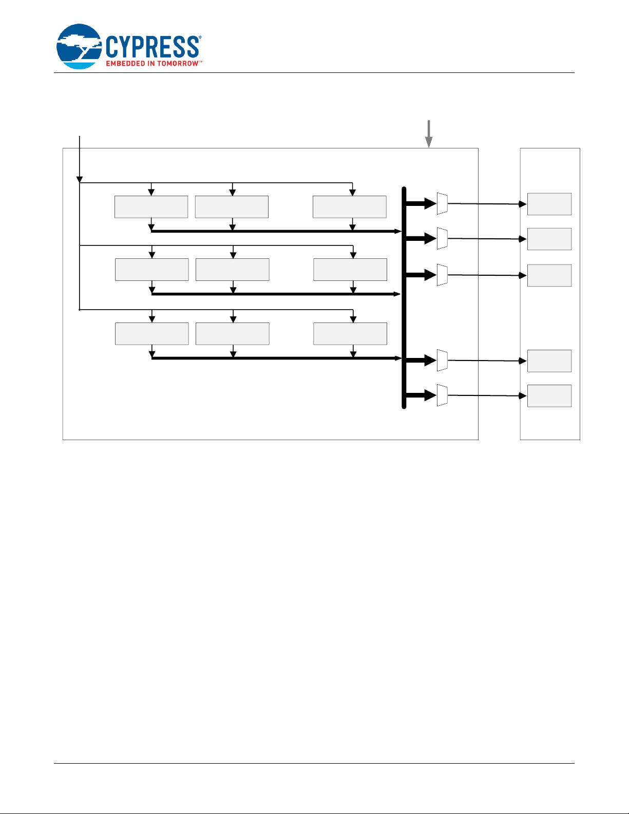
Figure 3. Peripheral Clock Dividers
8.0 divider 8.0 divider 8.0 divider
CLOCK_CTL[32]
CLK_PERI
DIV_CMD
Enable Selected Divider
Peripheral Clock Dividers
Group0
Counter1
CLOCK_CTL[31]
Group0
Counter0
Group0
Counter2
CLOCK_CTL[33]
CLOCK_CTL[107]
Group2
Counter1
CLOCK_CTL[106]
Group2
Counter0
.. .. ..
16.0 divider 16.0 divider 16.0 divider
.. .. ..
24.5 divider 24.5 divider 24.5 divider
.. .. ..
clk_counter
clk_counter
clk_counter
clk_counter
clk_counter
TCPWM
.. .. ..
...
...
#0 #1 #l
#0 #1 #m
#0 #1 #n
PERI_DIV_24_5_CTL
PERI_DIV_16_CTL
PERI_DIV_8_CTL
Peripheral clock dividers include three types of dividers: 8-bit divider (8.0 divider), 16-bit divider (16.0 divider), and
24.5-bit divider (24.5 divider). See the device datasheet for the number of each divider channels available for each
device.
Each divider makes a clock to divide clock CLK_PERI. 8-bit divider can divide CLK_PERI by 1 to 28 and 16-bit divider
can divide CLK_PERI by 1 to 216. And 24.5-bit divider is a divider which has 24 integer bits and 5 fractional bits.24-5bit
divider can divide CLK_PERI by 1 to 224 for integer and 1 to 25 for fractional.
That is, some counters run at the same clock frequency while another counter runs at a different clock frequency.
The following is an example for configuring peripheral clock dividers. This example shows the generation of three types
of clock frequencies: 40 MHz, 20 MHz, and 16 MHz. The source of those clocks is CLK_PERI 80 MHz.
1. Select the divider and set the divide number.
PERI_DIV_8_CTL_0.INT8_DIV = 1 /* set DVI_8[0] divider to 2. 80 MHz/2 = 40 MHz */
PERI_DIV_8_CTL_0.EN = 1
PERI_DIV_8_CTL_1.INT8_DIV = 3 /* set DVI_8[1] divider to 4. 80 MHz/4 = 20 MHz */
PERI_DIV_8_CTL_1.EN = 1
PERI_DIV_8_CTL_2.INT8_DIV = 4 /* set DVI_8[2] divider to 5. 80 MHz/5 = 16 MHz */
PERI_DIV_8_CTL_2.EN = 1
2. Enable the dividers.
PERI_DIV_CMD.DIV_SEL = 0 /* select divider number 0 */
PERI_DIV_CMD.TYPE_SEL = 0 /* select divider type DIV_8 */
PERI_DIV_CMD.ENABLE = 1 /* enable DIV_8[0] */
PERI_DIV_CMD.DIV_SEL = 1 /* select divider number 1 */
PERI_DIV_CMD.TYPE_SEL = 0 /* select divider type DIV_8 */
PERI_DIV_CMD.ENABLE = 1 /* enable DIV_8[1] */
Page 6
How to Use Timer, Counter, and PWM (TCPWM) in Traveo II Family
www.cypress.com Document Number: 002-20224 Rev. *B 5
PERI_DIV_CMD.DIV_SEL = 2 /* select divider number 2 */
PERI_DIV_CMD.TYPE_SEL = 0 /* select divider type DIV_8 */
PERI_DIV_CMD.ENABLE = 1 /* enable DIV_8[2] */
Following shows an example where the counter in TCPWM selects a clock configured in the peripheral clock
dividers example.
16-bit counter group0 counter0 selects a 16 MHz clk_counter clock, 16-bit counter group0 counter1 and counter2
select 20 MHz clk_counter clock, and 32-bit counter gropup2 counter0 to counter1 select 40 MHz clk_counter clock.
3. Select a clk_counter clock for each counter in TCPWM.
PERI _CLOCK_CTL_31.DIV_SEL = 0 /* select divider number 0 */
PERI _CLOCK_CTL_31.TYPE_SEL = 0 /* select divider type DIV_8 */
PERI _CLOCK_CTL_32.DIV_SEL = 1 /* select divider number 1 */
PERI _CLOCK_CTL_32.TYPE_SEL = 0 /* select divider type DIV_8 */
PERI _CLOCK_CTL_33.DIV_SEL = 1 /* select divider number 1 */
PERI _CLOCK_CTL_33.TYPE_SEL = 0 /* select divider type DIV_8 */
PERI _CLOCK_CTL_106.DIV_SEL = 2 /* select divider number 2 */
PERI _CLOCK_CTL_106.TYPE_SEL = 0 /* select divider type DIV_8 */
PERI _CLOCK_CTL_107.DIV_SEL = 2 /* select divider number 2 */
PERI _CLOCK_CTL_107.TYPE_SEL = 0 /* select divider type DIV_8 */
The output of the peripheral clock divider, clk_counter clock, has a unique number for each peripheral module. The
counter in TCPWM has a unique counter number. Table 2 shows the counter number in TCPWM of CYT2B7 series.
Regarding other series, see the device datasheet for Peripheral Clocks.
Table 2. CYT2B7 Series: Counter Number in TCPWM
Clock Number
Description
31:93
TCPWM group #0, 16-bit counter #0 to #62 (63 ch)
94:105
TCPWM group #1, 16-bit counter for motor #0 to #11 (12 ch)
106:109
TCPWM group #2, 32-bit counter #0 to #3 (4 ch)
3 TCPWM Operation Examples
3.1 Timer Mode
This section describes how to set up Timer Mode.
Timer Mode is for a basic counter application. This is ordinary counter usage to count the clock for timer.
The following are the different modes of counters based on the direction:
▪
COUNT_UP: Counting mode in the upward direction
▪
COUNT_DOWN: Counting mode in the downward direction
▪
UPDOWN-COUNTER1 and UPDOWN-COUNTER2: Counting mode in the upward and downward directions
Figure 4 shows Timer Mode in upward counting mode.
Page 7

How to Use Timer, Counter, and PWM (TCPWM) in Traveo II Family
www.cypress.com Document Number: 002-20224 Rev. *B 6
Figure 4. Timer Mode in Upward Counting Mode
10
0
5
15
Overflow (OV)
PERIOD = 15
CC0 = 4
COUNTER starts with 10"
CC0 = 8
Terminal Count (TC)
cc0_match
CC0 = 8 CC0 = 8
CC0 = 4
period is PERIOD + 1
Counter starts from initial value. Configured counter register as COUNTER = 10, then counter starts with 10.
Counter generates events depending on the counter value. There are five events: Underflow (UV), Overflow (OV),
Terminal Count (TC), cc0_match, and cc1_match. The event generation depends on the combination of Operation
Mode and UP_DOWN_MODE. Underflow event is not generated in COUNT_UP.
Overflow event is generated in the counter in which the counter value equals the PERIOD register value.
cc0_match event is generated in the counter in which the counter value equals the CC0 register value. CC0 value
can be switched with CC0_BUF value at the cc0_match event point. CC0 and CC0_BUF values are configured by the
related register bits. Figure 4 shows that the CC0 register value is 8 and the CC0_BUF register value is 4 at the start
point, and then the CC0 register value is changed to 4 and the CC0_BUF register value is changed to 8 at the
cc0_match point.
Figure 5 shows the timer functionality which includes the events and interrupt, tr_out0 and tr_out1 relationship.
Figure 5. Timer Functionality
CC0/1
PERIOD
COUNTER
==
CC0/1
==
==
CC0/1
CC0/1_BUF
Interrupt
generation
Trigger
generation
Terminal Count
Underflow
Overflow
cc0_match
cc1_match
tr_out0
tr_out1
interrupt
equal
equal
Every event can be output as trigger tr_out0, tr_out1, or an interrupt from the counter in TCPWM to other modules.
For example, in the use case of specific interval data translation by P-DMA, a periodic trigger is generated by
cc0_match and this cc0_match is used as trigger to activate P-DMA. This trigger and P-DMA connection are handled
by the Triggers Multiplexer module.
Page 8

How to Use Timer, Counter, and PWM (TCPWM) in Traveo II Family
www.cypress.com Document Number: 002-20224 Rev. *B 7
The following is an example for configuring the Timer Mode using a 16-bit counter: The Terminal Count (TC) event
causes an interrupt for a counter period 1 second at 15625 Hz counter clock.
1. Set the CTRL register; CNT_CTRL = 0x00000001.
TCPWM_GRP_CNT_CTRL.AUTO_RELOAD_CC0 = 0 /* Never Switch */
TCPWM_GRP_CNT_CTRL.UP_DOWN_MODE = 0 /* COUNT_UP */
TCPWM_GRP_CNT_CTRL.ONE_SHOT = 0 /* Counter runs continuous */
TCPWM_GRP_CNT_CTRL.MODE = 0 /* Timer Mode */
TCPWM_GRP_CNT_CTRL.DBG_FREEZE_EN = 0 /* Counter operation continues in debug mode */
TCPWM_GRP_CNT_CTRL.ENABLED = 0 /* Counter disabled */
2. Set the PERIOD register; PERIOD = 0xF
TCPWM_GRP_CNT_PERIOD.PERIOD = 15624 /* Counter period “PERIOD + 1” */
3. Set the COUNTER register; COUNTER = 0x0
TCPWM_GRP_CNT_COUNTER.COUNTER = 0 /* Counter starts with 0 */
4. Set the INTR_MASK register; INTR_MASK = 0x1
TCPWM_GRP_CNT_INTR_MASK.TC = 1 /* TC Interrupt enabled */
5. Set the CTRL register to enable the counter;
TCPWM_GRP_CNT_CTRL.ENABLED = 1 /* Counter enabled */
6. Set the TR_CMD register to start the counter;
TCPWM_GRP_CNT_TR_CMD.STRT = 1 /* Counter start by software trigger */
3.2 Capture Mode
This section describes how to set up Capture Mode.
This Capture Mode is for an application to catch the counter value depending on the input trigger.
Figure 6 shows the Capture Mode in upward counting mode.
Figure 6. Capture Mode in Upward Counting Mode
10
0
5
15
Overflow (OV)
PERIOD = 15
Capture
Event
Terminal Count (TC)
cc0_match
period is PERIOD + 1
Capture
Event
Capture
Event
8 15
4
8
15
CC0
CC0_BUFF
When the trigger input is detected, the Capture Event occurs, and the counter value is captured in the CC0 register.
Also, cc0_match event is generated.
Page 9

How to Use Timer, Counter, and PWM (TCPWM) in Traveo II Family
www.cypress.com Document Number: 002-20224 Rev. *B 8
When the next cc0_match event occurs, the CC0 register value is copied to the CC0_BUFF register and the counter
value is captured in the CC0 register.
The counter in TCPWM can select the input trigger from the input trigger sources. See the device datasheet for the
number of each counter channels available for each device.
Table 3 shows the input trigger sources of the 16-bit counter number 0 in the CYT2B7 series.
Table 3. CYT2B7 Series: Trigger Inputs List of 16-bit Counter Number 0
Trigger No.
Input Trigger
Input Trigger Sources
0
Constant 0
Always 0 input (Not counting)
1
Constant 1
Always 1 input (Counting with a clock)
2
tr_one_cnt_in[0]
TC_0_TR0 (P3.1 or P6.1)
3
tr_one_cnt_in[1]
TC_0_TR1 (P3.2 or P6.2)
4
tr_one_cnt_in[2]
PASS (SAR ADC) Range violation ADC0 ch.4
20:5
tr_all_cnt_in[15:0]
Select one source from connected triggers in MUX_4 group
31:21
tr_all_cnt_in[26:16]
Select one source from connected triggers in MUX_5 group
TCPWM can configure the input trigger as several events. Capture Mode can use six events; reload, start, stop, count,
capture0, and capture1.
The following is an example for configuring the Capture Mode using a 16-bit counter and input trigger from I/O port as
the capture0 event. Relevant I/O port should be configured as TCPWM input resource of TC_x_TR0/1:
1. Set the CTRL register; CNT_CTRL = 0x02000000.
TCPWM_GRP_CNT_CTRL.AUTO_RELOAD_CC0 = 0 /* This field does not have a function
in Capture mode */
TCPWM_GRP_CNT_CTRL.UP_DOWN_MODE = 0 /* COUNT_UP */
TCPWM_GRP_CNT_CTRL.ONE_SHOT = 0 /* Counter runs continuous */
TCPWM_GRP_CNT_CTRL.MODE = 2 /* Capture Mode */
TCPWM_GRP_CNT_CTRL.DBG_FREEZE_EN = 0 /* Counter operation continues in debug mode */
TCPWM_GRP_CNT_CTRL.ENABLED = 0 /* Counter disabled */
2. Set the PERIOD register; PERIOD = 0xF.
TCPWM_GRP_CNT_PERIOD.PERIOD = 15 /* Counter period “PERIOD + 1” */
3. Set the COUNTER register; COUNTER = 0x0
TCPWM_GRP_CNT_COUNTER.COUNTER = 0 /* Counter starts with 0 */
4. Set the TR_IN_SEL0 register for select input trigger; TR_IN_SEL0 = 0x0102
TCPWM_GRP_CNT_TR_IN_SEL0.CAPTURE0_SEL = 2 /* tr_one_cnt_in[0] trigger */
TCPWM_GRP_CNT_TR_IN_SEL0.COUNT_SEL = 1 /* Constant 1: Counting with a clock */
5. Set the TR_IN_EDGE_SEL register to capture the edge of the input trigger; TR_IN_EDGE_SEL = 0xFFE
TCPWM_GRP_CNT_TR_IN_EDGE_SEL.CAPTURE0_EDGE = 2 /* Any Edge: Rising and Falling edge */
6. Set the CC0 register; CC0 = 0x0
TCPWM_GRP_CNT_CC0.CC = 0 /* cc0 0 */
7. Set the CC0_BUF register; CC0_BUFF = 0x0
TCPWM_GRP_CNT_CC0_BUFF.CC = 0 /* cc0_buff 0 */
8. Set the TR_OUT_SEL register; TR_OUT_SEL = 0x77
TCPWM_GRP_CNT_TR_OUT_SEL.OUT0 = 7 /* tr_out0 disabled */
Page 10

How to Use Timer, Counter, and PWM (TCPWM) in Traveo II Family
www.cypress.com Document Number: 002-20224 Rev. *B 9
TCPWM_GRP_CNT_TR_OUT_SEL.OUT1 = 7 /* tr_out1 disabled */
9. Set the CTRL register to enable the counter;
TCPWM_GRP_CNT_CTRL.ENABLED = 1 /* Counter enabled */
10. Set the TR_CMD register to start the counter;
TCPWM_GRP_CNT_TR_CMD.STRT = 1 /* Counter start by software trigger */
3.3 PWM Mode
This section describes how to set up the PWM Mode.
PWM Mode is for an application to output the Pulse Width Modulated signal on the line_out and line_compl_out.
Figure 7 shows PWM Mode in upward counting mode.
Figure 7. PWM Mode in Up Counting Mode
10
0
5
15
Overflow (OV)
PERIOD = 15
CC1 = 4
COUNTER starts with 10"
CC0 = 8
Terminal Count (TC)
cc0_match
CC0 = 8
CC0 = 8
CC1 = 4
period is PERIOD + 1
line_out
cc1_match
CC1 = 4
line_compl_out
PWM signal frequency is configured by the PERIOD register. This PWM signal period is the value of PERIOD register
plus 1. PWM Duty is configured by CC0 or CC1 register. cc0_match and cc1_match events in PWM Mode occur at the
configured COUNTER value.
PWM signal is generated to use Overflow, Underflow, cc0_match, and cc1_match events.
Figure 8 shows line generation logic. TR_PWM_CTL controls the line state change as per four events: Underflow,
Overflow, cc0_match, and cc1_match.
Figure 8. Line Generation Logic
PWM
Generation
Underflow
Overflow
cc0_match
cc1_match
Line
Select
line
Kill
Period
line_out polarity
line_compl_out polarity
line_out
line_compl_out
TR_PWM_CTL
Page 11

How to Use Timer, Counter, and PWM (TCPWM) in Traveo II Family
www.cypress.com Document Number: 002-20224 Rev. *B 10
There are two output lines: a PWM signal is output from line_out, and a complementary PMW signal is output from
line_compl_out. Relevant I/O port is configured as PWM output resource, line_out, and line_compl_out are output by
PWM and PWM_N port.
The polarity of both line_out signals can be configured in the CTRL register. The QUAD_ENCODING_MODE[0] bit sets
the polarity of line_out; QUAD_ENCODING_MODE[1] bit can be used to set the polarity of line_compl_out. The value
‘1’ inverts the corresponding line_out signals.
Kill period input will disable both line_out and line_compl_out. The Kill mode is specified by the PWM_IMM_KILL,
PWM_STOP_ON_KILL, and PWM_SYNC_KILL registers.
Counter point is configured by the COUNTER register. In Figure 7, beginning from “10” counter point, configured by
the COUNTER register, to “15” first Overflow event period is set as waiting time.
Four internal events, Underflow, Overflow, cc0_match, and cc1_mach, can be used to output the trigger. In Figure 7,
cc1_match event can be configured with CC1 register in the flexible point within a period. This cc1_match event is used
to activate trigger for other modules such as SAR ADC.
The following is an example for configuring the PWM Mode using a 16-bit counter. PWM signal is generated with
Overflow and cc0_match event, and cc1_match event is output as the trigger output.
1. Set the CTRL register; CNT_CTRL = 0x04000000
TCPWM_GRP_CNT_CTRL.AUTO_RELOAD_CC0 = 0
/* Never switch */
TCPWM_GRP_CNT_CTRL.AUTO_RELOAD_CC1 = 0
/* Never switch */
TCPWM_GRP_CNT_CTRL.AUTO_RELOAD_PERIOD = 0
/* Never switch */
TCPWM_GRP_CNT_CTRL.AUTO_RELOAD_LINE_SEL = 0
/* Never switch */
TCPWM_GRP_CNT_CTRL.CC0_MATCH_UP_EN = 0
/* This bit is only for 16-bit
counter for Motor control */
TCPWM_GRP_CNT_CTRL.CC0_MATCH_DOWN_EN = 0
/* This bit is only for 16-bit
counter for Motor control */
TCPWM_GRP_CNT_CTRL.CC1_MATCH_UP_EN = 0
/* This bit is only for 16-bit counter
for Motor control */
TCPWM_GRP_CNT_CTRL.CC1_MATCH_DOWN_EN = 0
/* This bit is only for 16-bit
counter for Motor control */
TCPWM_GRP_CNT_CTRL.PWM_IMM_KILL = 0
/* Synchronous kill activation */
TCPWM_GRP_CNT_CTRL.PWM_STOP_ON_KILL = 0
/* Kill event does NOT stop counter
*/
TCPWM_GRP_CNT_CTRL.PWM_SYNC_KILL = 0
/* Synchronous kill mode */
TCPWM_GRP_CNT_CTRL.PWM_DISABLE_MODE = 0
/* When the counter is disabled the
PWM outputs "line_out" and
"line_compl_out" are NOT
driven by the TCPWM. Instead the
port default level configuration
applies. */
TCPWM_GRP_CNT_CTRL.UP_DOWN_MODE = 0
/* COUNT_UP */
TCPWM_GRP_CNT_CTRL.ONE_SHOT = 0
/* Counter runs continuous */
TCPWM_GRP_CNT_CTRL.QUAD_ENCODING_MODE = 0
/* In PWM, PWM_DT and PWM_PR Modes,
these two bits can be used to invert
“line_out” and “line_compl_out”. */
TCPWM_GRP_CNT_CTRL.MODE = 4
/* PWM Mode */
TCPWM_GRP_CNT_CTRL.DBG_FREEZE_EN = 0
/* Counter operation continues in
debug mode */
TCPWM_GRP_CNT_CTRL.ENABLED = 0
/* Counter disabled */
2. Set the PERIOD register; PERIOD = 0xF.
TCPWM_GRP_CNT_PERIOD.PERIOD = 15 /* Counter period “PERIOD + 1” */
3. Set the COUNTER register; COUNTER = 0xA.
TCPWM_GRP_CNT_COUNTER.COUNTER = 10 /* Counter starts with 10 */
Page 12

How to Use Timer, Counter, and PWM (TCPWM) in Traveo II Family
www.cypress.com Document Number: 002-20224 Rev. *B 11
4. Set the CC0 register; CC0 = 0x8.
TCPWM_GRP_CNT_CC0.CC = 8 /* cc0 8 */
5. Set the CC1 register; CC1 = 0x4.
TCPWM_GRP_CNT_CC1.CC = 4 /* cc1 4 */
6. Set the TR_PWM_CTRL register; TR_PWM_CTRL = 0xF1.
TCPWM_GRP_CNT_TR_PWM_CTRL.CC0_MATCH_MODE = 1 /* cc0_match event Set to 0 */
TCPWM_GRP_CNT_TR_PWM_CTRL.OVERFLOW_MODE = 0 /* Overflow event Set to 1 */
TCPWM_GRP_CNT_TR_PWM_CTRL.UNDERFLOW_MODE = 3 /* Underflow event No change */
TCPWM_GRP_CNT_TR_PWM_CTRL.CC1_MATCH_MODE = 3 /* cc1_match event No change */
7. Set the TR_OUT_SEL register; TR_OUT_SEL = 0x47.
TCPWM_GRP_CNT_TR_OUT_SEL.OUT0 = 7 /* tr_out0 disabled */
TCPWM_GRP_CNT_TR_OUT_SEL.OUT1 = 4 /* tr_out1 cc1_match */
8. Set the CTRL register to enable the counter;
TCPWM_GRP_CNT_CTRL.ENABLED = 1 /* Counter enabled */
9. Set the TR_CMD register to start the counter;
TCPWM_GRP_CNT_TR_CMD.STRT = 1 /* Counter start by software trigger */
3.4 PWM Dead Time (PWM_DT) Mode
This section describes how to set up PWM_DT Mode.
PWM_DT Mode is for an application to output the PWM signal with Dead Time on the line_out and line_compl_out.
Figure 9 shows PWM_DT Mode in up counting mode.
Figure 9. Counting Behavior for PWM_DT Mode
10
0
5
15
Overflow (OV)
PERIOD = 15
CC1 = 4
COUNTER starts with 10"
CC0 = 8
Terminal Count (TC)
cc0_match
CC0 = 8
CC0 = 8
CC1 = 4
period is PERIOD + 1
line_out
cc1_match
CC1 = 4
line_compl_out
Dead Time
Dead Time Dead Time
Dead Time Dead Time
Dead Time
PWM signal with Dead Time is configured like the PWM Mode. PWM_DT Mode is similar to the PWM Mode. PWM
signal in PWM_DT Mode has a Dead Time.
Page 13

How to Use Timer, Counter, and PWM (TCPWM) in Traveo II Family
www.cypress.com Document Number: 002-20224 Rev. *B 12
The definition of Dead Time is configured by the DT_LINE_OUT_L bits in the DT register. Dead Time is added to each
PWM rising edge of line_out and line_compl_out. Dead Time width of both line_out signals is the same.
The 16-bit counter for motors has advanced motor control features. The Dead Time for line_out can be configured by
DT_LINE_OUT_L and DT_LINE_OUT_H bits in the DT register, and the Dead Time for line_compl_out can be
configured by DT_LINE_COMPL_OUT bits in the DT register. Dead Time width of Line_out and line_compl_out can be
set different values.
The following is an example for configuring the PWM_DT Mode using a 16-bit counter. PWM signal is generated with
Overflow and cc0_match event, and cc1_match event is output as the trigger output.
1. Set the CTRL register; CNT_CTRL = 0x05000000
TCPWM_GRP_CNT_CTRL.AUTO_RELOAD_CC0 = 0 /* Never switch */
TCPWM_GRP_CNT_CTRL.AUTO_RELOAD_CC1 = 0 /* Never switch */
TCPWM_GRP_CNT_CTRL.AUTO_RELOAD_PERIOD = 0 /* Never switch */
TCPWM_GRP_CNT_CTRL.AUTO_RELOAD_LINE_SEL = 0 /* Never switch */
TCPWM_GRP_CNT_CTRL.CC0_MATCH_UP_EN = 0 /* This bit is only for 16-bit counter
for Motor Control */
TCPWM_GRP_CNT_CTRL.CC0_MATCH_DOWN_EN = 0 /* This bit is only for 16-bit counter
for Motor Control */
TCPWM_GRP_CNT_CTRL.CC1_MATCH_UP_EN = 0 /* This bit is only for 16-bit counter
for Motor Control */
TCPWM_GRP_CNT_CTRL.CC1_MATCH_DOWN_EN = 0 /* This bit is only for 16-bit counter
for Motor Control */
TCPWM_GRP_CNT_CTRL.PWM_IMM_KILL = 0 /* Synchronous kill activation */
TCPWM_GRP_CNT_CTRL.PWM_STOP_ON_KILL = 0 /* Kill event does NOT stop counter */
TCPWM_GRP_CNT_CTRL.PWM_SYNC_KILL = 0 /* Synchronous kill mode */
TCPWM_GRP_CNT_CTRL.PWM_DISABLE_MODE = 0 /* When the counter is disabled the
PWM outputs "line_out" and
"line_compl_out" are NOT
driven by the TCPWM. Instead the
port default
level configuration applies. */
TCPWM_GRP_CNT_CTRL.UP_DOWN_MODE = 0 /* COUNT_UP */
TCPWM_GRP_CNT_CTRL.ONE_SHOT = 0 /* Counter runs continuous */
TCPWM_GRP_CNT_CTRL.QUAD_ENCODING_MODE = 0 /* In PWM, PWM_DT and PWM_PR Modes,
these two bits can be used to
invert “line_out” and
“line_compl_out”. */
TCPWM_GRP_CNT_CTRL.MODE = 5 /* PWM_DT Mode */
TCPWM_GRP_CNT_CTRL.DBG_FREEZE_EN = 0 /* Counter operation continues in
debug mode */
TCPWM_GRP_CNT_CTRL.ENABLED = 0 /* Counter disabled */
2. Set the PERIOD register; PERIOD = 0xF.
TCPWM_GRP_CNT_PERIOD.PERIOD = 15 /* Counter period “PERIOD + 1” */
3. Set the COUNTER register; COUNTER = 0xA.
TCPWM_GRP_CNT_COUNTER.COUNTER = 10 /* Counter starts with 10 */
4. Set the CC0 register; CC0 = 0x8.
TCPWM_GRP_CNT_CC0.CC = 8 /* cc0 8 */
5. Set the CC1 register; CC1 = 0x4
TCPWM_GRP_CNT_CC1.CC = 4 /* cc1 4 */
6. Set the DT register for Dead Time; DT = 0x0002.
TCPWM_GRP_CNT_DT.DT_LINE_OUT_L = 2 /* Dead Time 2 */
Page 14

How to Use Timer, Counter, and PWM (TCPWM) in Traveo II Family
www.cypress.com Document Number: 002-20224 Rev. *B 13
TCPWM_GRP_CNT_DT.DT_LINE_OUT_H = 0 /* This field is used in 16bit counter
for motor */
TCPWM_GRP_CNT_DT.DT_LINE_COMPL_OUT = 0 /* This field is used in 16bit counter
for motor */
7. Set the TR_PWM_CTRL register; TR_PWM_CTRL = 0xF1.
TCPWM_GRP_CNT_TR_PWM_CTRL.CC0_MATCH_MODE = 1 /* cc0_match event Set to 0 */
TCPWM_GRP_CNT_TR_PWM_CTRL.OVERFLOW_MODE = 0 /* Overflow event Set to 1 */
TCPWM_GRP_CNT_TR_PWM_CTRL.UNDERFLOW_MODE = 3 /* Underflow event No change */
TCPWM_GRP_CNT_TR_PWM_CTRL.CC1_MATCH_MODE = 3 /* cc1_match event No change */
8. Set the LINE_SEL register; LINE_SEL = 0x32.
TCPWM_GRP_CNT_LINE_SEL.OUT_SEL = 2 /* PWM signal “line” */
TCPWM_GRP_CNT_LINE_SEL.COMPL_OUT_SEL = 3 /* inverted PWM signal “line” */
9. Set the TR_OUT_SEL register; TR_OUT_SEL = 0x47.
TCPWM_GRP_CNT_TR_OUT_SEL.OUT0 = 7 /* tr_out0 disabled */
TCPWM_GRP_CNT_TR_OUT_SEL.OUT1 = 4 /* tr_out1 cc1_match */
10. Set the CTRL register to enable the counter.
TCPWM_GRP_CNT_CTRL.ENABLED = 1 /* Counter enabled */
11. Set the TR_CMD register to start the counter.
TCPWM_GRP_CNT_TR_CMD.STRT = 1 /* Counter start by software trigger */
3.5 Relation of Trigger Multiplexer
Traveo II family has the Trigger Multiplexer module. TCPWM uses the Trigger Multiplexer to connect modules, such as
SAR ADC, P-DMA, and TCPWM itself. See the device datasheet for the Trigger Multiplexer connection for each device.
Figure 10 shows an example to use Triger Multiplexer for starting three counters of TCPWM simultaneously to output
PMW signals. These counters use the same input trigger for starting the event. This input trigger is configured by the
Trigger Multiplexer.
Figure 10. Three Counters of TCPWM Start with a Trigger
Group0
Counter0
Group0
Counter1
Group0
Counter2
Trigger Multiplexer
tr_all_cnt_in[0]
Group4, #0
TCPWM
PWM
PWM
PWM
Trigger Multiplexer has two types of connection. Group connection and one-to-one connection.
The following shows an example for configuring CYT2B7 series using group connection. The trigger is number0 of
tr_all_cnt_in of Group4. This trigger starts counters.
1. Set the TR_IN_SEL1 register to select the input trigger for the start event.
TCPWM_GRP_CNT_TR_IN_SEL1.START_SEL = 5 /* select tr_one_cnt_in[0] in table.3 */
2. Set the TR_IN_EDGE_SEL register to select the input trigger edge.
TCPWM_GRP_CNT_TR_IN_EDGE_SEL.START_EDGE = 0 /* select rising edge */
Page 15

How to Use Timer, Counter, and PWM (TCPWM) in Traveo II Family
www.cypress.com Document Number: 002-20224 Rev. *B 14
3. Set the TR_CMD register to output the trigger from Trigger Multiplexer.
PERI_TR_CMD.TR_SEL = 0 /* select trigger number 0 */
PERI_TR_CMD.GROUP_SEL = 4 /* select group 4 */
PERI_TR_CMD.TR_EDGE = 0 /* 0: level sensitive */
PERI_TR_CMD.OUT_SEL = 1 /* 1: Output trigger */
PERI_TR_CMD.ACTIVATE = 1 /* 1: Activate */
Figure 11 shows an example to use Trigger Multiplexer to activate SAR ADC using the output trigger of TCPWM.
Tr_out1 output from TCPWM and the trigger for SAR ADC are connected through one-to-one connection of Trigger
Multiplexer.
In this example, the timing of cc1 match event is configurable. Also, tr_out1 can select the cc1 match event as a
trigger. See PWM Mode and PWM Dead Time (PWM_DT) Mode for details on cc1 match event.
Figure 11. Relation of Trigger Multiplexer, TCPWM, and SAR ADC
Group0
Counter0
Group0
Counter1
Group0
Counter2
TCPWM
Tr_out1[1]
Tr_out1[2]
Tr_out1[0]
Trigger Multiplexer
One to One trigger
Connect Direct to
SAR ADC
Group 1
ADC 0
channel 4
ADC 0
channel 5
ADC 0
channel 6
SAR ADC
trigger
trigger
trigger
Analog Input
ADC[0]_0
ADC[0]_2
ADC[0]_4
The logical channel of SAR ADC can select the Analog input port channel from the same unit number of SAR ADC.
The logical channel in SAR ADC unit 0 can select the Analog input port from ADC 0 port.
The following is an example for trigger configuration of CYT2B7 series. Figure 11 is combination of 16-bit counter of
TCPWM and SAR ADC through the one-to-one connection of Trigger Multiplexer.
1. Set the PERI_TR_1TO1_GR_TR_CTL register to enable the corresponding Trigger Multiplexer. Input trigger
setting is 1.
2. Set the SAR_CH_TR_CTL register to select activate trigger number of SAR ADC. A trigger number of TCPWM
is 1.
4 Glossary
Terms
Description
SAR ADC
Analog-to-digital converter. See the SAR ADC chapter of Architecture TRM for details.
P-DMA
Peripheral DMA
Peripheral Clock
Divider
Peripheral Clock Divider derive a clock to use of each peripheral function such as counters in TCPWM.
Trigger multiplexer
A trigger multiplexer routes triggers from a source peripheral to a destination. See the Trigger Multiplexer chapter
of Architecture TRM for details.
Page 16

How to Use Timer, Counter, and PWM (TCPWM) in Traveo II Family
www.cypress.com Document Number: 002-20224 Rev. *B 15
5 Related Documents
The following are the Traveo II family series datasheets and Technical Reference Manuals. Contact Technical Support
to obtain these documents.
▪
Device datasheet
CYT2B7 Datasheet 32-Bit Arm® Cortex®-M4F Microcontroller Traveo™ II Family
CYT2B9 Datasheet 32-Bit Arm® Cortex®-M4F Microcontroller Traveo™ II Family
CYT4BF Datasheet 32-Bit Arm® Cortex®-M7 Microcontroller Traveo™ II Family
CYT4DN Datasheet 32-Bit Arm® Cortex®-M7 Microcontroller Traveo™ II Family
CYT3BB/4BB Datasheet 32-Bit Arm® Cortex®-M7 Microcontroller Traveo™ II Family
▪
Body Controller Entry Family
Traveo™ II Automotive Body Controller Entry Family Architecture Technical Reference Manual (TRM)
Traveo™ II Automotive Body Controller Entry Registers Technical Reference Manual (TRM) for CYT2B7
Traveo™ II Automotive Body Controller Entry Registers Technical Reference Manual (TRM) for CYT2B9
▪
Body Controller High Family
Traveo™ II Automotive Body Controller High Family Architecture Technical Reference Manual (TRM)
Traveo™ II Automotive Body Controller High Registers Technical Reference Manual (TRM) for CYT4BF
Traveo™ II Automotive Body Controller High Registers Technical Reference Manual (TRM) for CYT3BB/4BB
▪
Cluster 2D Family
Traveo™ II Automotive Cluster 2D Family Architecture Technical Reference Manual (TRM)
Traveo™ II Automotive Cluster 2D Registers Technical Reference Manual (TRM)
Page 17

How to Use Timer, Counter, and PWM (TCPWM) in Traveo II Family
www.cypress.com Document Number: 002-20224 Rev. *B 16
Document History
Document Title: AN220224 - How to Use Timer, Counter, and PWM (TCPWM) in Traveo II Family
Document Number: 002-20224
Revision
ECN
Submission
Date
Description of Change
**
6103855
06/26/2019
New Application Note.
*A
6719536
10/31/2019
Added CYT4D Series
*B
6810474
03/11/2020
Changed target parts number (CYT2/CYT4 series).
Added target parts number (CYT3 series).
Page 18

How to Use Timer, Counter, and PWM (TCPWM) in Traveo II Family
www.cypress.com Document Number: 002-20224 Rev. *B 17
Worldwide Sales and Design Support
Cypress maintains a worldwide network of offices, solution centers, manufacturer’s representatives, and distributors. To find the
office closest to you, visit us at Cypress Locations.
Products
Arm® Cortex® Microcontrollers
cypress.com/arm
Automotive
cypress.com/automotive
Clocks & Buffers
cypress.com/clocks
Interface
cypress.com/interface
Internet of Things
cypress.com/iot
Memory
cypress.com/memory
Microcontrollers
cypress.com/mcu
PSoC
cypress.com/psoc
Power Management ICs
cypress.com/pmic
Touch Sensing
cypress.com/touch
USB Controllers
cypress.com/usb
Wireless Connectivity
cypress.com/wireless
PSoC® Solutions
PSoC 1 | PSoC 3 | PSoC 4 | PSoC 5LP | PSoC 6 MCU
Cypress Developer Community
Community | Code Examples | Projects | Videos | Blogs |
Training | Components
Technical Support
cypress.com/support
All other trademarks or registered trademarks referenced herein are the property of their respective owners.
© Cypress Semiconductor Corporation, 2019-2020. This document is the property of Cypress Semiconductor Corporation and its subsidiaries (“Cypress”). This
document, including any software or firmware included or referenced in this document (“Software”), is owned by Cypress under the intellectual property laws and
treaties of the United States and other countries worldwide. Cypress reserves all rights under such laws and treaties and does not, except as specifically stated in
this paragraph, grant any license under its patents, copyrights, trademarks, or other intellectual property rights. If the Software is not accompanied by a license
agreement and you do not otherwise have a written agreement with Cypress governing the use of the Software, then Cypress hereby grants you a personal, nonexclusive, nontransferable license (without the right to sublicense) (1) under its copyright rights in the Software (a) for Software provided in source code form, to
modify and reproduce the Software solely for use with Cypress hardware products, only internally within your organization, and (b) to distribute the Software in binary
code form externally to end users (either directly or indirectly through resellers and distributors), solely for use on Cypress hardware product units, and (2) under
those claims of Cypress’s patents that are infringed by the Software (as provided by Cypress, unmodified) to make, use, distr ibute, and import the Software solely
for use with Cypress hardware products. Any other use, reproduction, modification, translation, or compilation of the Software is prohibited.
TO THE EXTENT PERMITTED BY APPLICABLE LAW, CYPRESS MAKES NO WARRANTY OF ANY KIND, EXPRESS OR IMPLIED, WITH REGARD TO THIS
DOCUMENT OR ANY SOFTWARE OR ACCOMPANYING HARDWARE, INCLUDING, BUT NOT LIMITED TO, THE IMPLIED WARRANTIES OF
MERCHANTABILITY AND FITNESS FOR A PARTICULAR PURPOSE. No computing device can be absolutely secure. Therefore, despite security measures
implemented in Cypress hardware or software products, Cypress shall have no liability arising out of any security breach, such as unauthorized access to or use of
a Cypress product. CYPRESS DOES NOT REPRESENT, WARRANT, OR GUARANTEE THAT CYPRESS PRODUCTS, OR SYSTEMS CREATED USING
CYPRESS PRODUCTS, WILL BE FREE FROM CORRUPTION, ATTACK, VIRUSES, INTERFERENCE, HACKING, DATA LOSS OR THEFT, OR OTHER
SECURITY INTRUSION (collectively, “Security Breach”). Cypress disclaims any liability relating to any Security Breach, and y ou shall and hereby do release
Cypress from any claim, damage, or other liability arising from any Security Breach. In addition, the products described in these materials may contain design
defects or errors known as errata which may cause the product to deviate from published specifications. To the extent permitted by applicable law, Cypress reserves
the right to make changes to this document without further notice. Cypress does not assume any liability arising out of the application or use of any product or circuit
described in this document. Any information provided in this document, including any sample design information or programming code, is provided only for reference
purposes. It is the responsibility of the user of this document to properly design, program, and test the functionality and safety of any application made of this
information and any resulting product. “High-Risk Device” means any device or system whose failure could cause personal injury, death, or property damage.
Examples of High-Risk Devices are weapons, nuclear installations, surgical implants, and other medical devices. “Critical Component” means any component of a
High-Risk Device whose failure to perform can be reasonably expected to cause, directly or indirectly, the failure of the High-Risk Device, or to affect its safety or
effectiveness. Cypress is not liable, in whole or in part, and you shall and hereby do release Cypress from any claim, damage, or other liability arising from any use
of a Cypress product as a Critical Component in a High-Risk Device. You shall indemnify and hold Cypress, its directors, officers, employees, agents, affiliates,
distributors, and assigns harmless from and against all claims, costs, damages, and expenses, arising out of any claim, including claims for product liability, personal
injury or death, or property damage arising from any use of a Cypress product as a Critical Component in a High-Risk Device. Cypress products are not intended
or authorized for use as a Critical Component in any High-Risk Device except to the limited extent that (i) Cypress’s published data sheet for the product explicitly
states Cypress has qualified the product for use in a specific High-Risk Device, or (ii) Cypress has given you advance written authorization to use the product as a
Critical Component in the specific High-Risk Device and you have signed a separate indemnification agreement.
Cypress, the Cypress logo, Spansion, the Spansion logo, and combinations thereof, WICED, PSoC, CapSense, EZ-USB, F-RAM, and Traveo are trademarks or
registered trademarks of Cypress in the United States and other countries. For a more complete list of Cypress trademarks, visit cypress.com. Other names and
brands may be claimed as property of their respective owners.
 Loading...