

Page 1

Please note that Cypress is an Infineon Technologies Company.
The document following this cover page is marked as “Cypress” document as this is the
company that originally developed the product. Please note that Infineon will continue
to oer the product to new and existing customers as part of the Infineon product
portfolio.
Continuity of document content
The fact that Infineon oers the following product as part of the Infineon product
portfolio does not lead to any changes to this document. Future revisions will occur
when appropriate, and any changes will be set out on the document history page.
Continuity of ordering part numbers
Infineon continues to support existing part numbers. Please continue to use the
ordering part numbers listed in the datasheet for ordering.
www.infineon.com
Page 2
www.cypress.com Document Number. 002-20191 Rev. *D 1
AN220191
How to Use Direct Memory Access (DMA) Controller in Traveo II Family
Author: Hitoshi Ogawa
Associated Part Family: Traveo™ II Family CYT2/CYT3/CYT4 Series
Related Application Notes: See Related Documents
This application note describes how to use DMA controllers (P-DMA and M-DMA) in Cypress Traveo II Family MCUs.
DMA controllers can transfer data from a source to a destination without CPU intervention. The application note
illustrates how to configure DMA for peripheral-to-memory, memory-to-peripheral, and memory-to-memory data
transfers.
Contents
1 Introduction .................................................................. 1
1.1 Features .............................................................. 2
1.2 Block Diagram ..................................................... 3
2 Operation Overview ..................................................... 5
2.1 Disable/Enable P-DMA/M-DMA .......................... 5
2.2 Configure Channel .............................................. 5
2.3 Configure Descriptor ........................................... 6
2.4 Disable/Enable P-DMA/M-DMA Channel .......... 12
3 P-DMA Use Cases .................................................... 12
3.1 1D Transfer (Memory-to-Peripheral) ................. 12
3.2 1D Transfer (Peripheral-to-Memory) ................. 14
3.3 Descriptor Chaining .......................................... 15
3.4 2D Transfer (Peripheral-to-Memory) ................. 18
3.5 CRC Transfer .................................................... 19
4 M-DMA Use Case ..................................................... 21
4.1 Memory-to-Memory (Memory Copy) ................. 21
5 Glossary .................................................................... 23
6 Related Documents ................................................... 24
Document History ............................................................ 25
Worldwide Sales and Design Support ............................. 26
1 Introduction
This application note describes how to use the Direct Memory Access (DMA) Controller in Cypress Traveo II family
MCUs.
DMA controllers can seamlessly transfer data between memory and on-chip peripherals, or between memories without
CPU intervention. This allows the CPU to handle other tasks while the DMA controller transfers data.
Both P-DMA and M-DMA have multiple independent DMA channels. Each DMA channel has a separate DMA request
input that initiates the transaction and can independently transfer data. See the device datasheet for the number of
DMA channels available for each device.
This series supports two types of DMA controllers: Peripheral DMA (P-DMA) and Memory DMA (M-DMA). P-DMA is
used for peripheral-to-memory and memory-to-peripheral low-latency data transfers for many channels. M-DMA is used
for memory-to-memory high-memory-bandwidth data transfer for a small number of channels.
These DMA controllers have a descriptor that specifies the transfer operation, and it corresponds flexibly to various
applications. Descriptors can be chained; it is possible to have circular lists.
This application note explains the functioning of DMA controllers in the series, initial configuration, and data transfer
operations with use cases.
To understand the functionality described and terminology used in this application note, see the “Direct Memory Access”
chapter of the Architecture Technical Reference Manual (TRM).
Page 3
How to Use Direct Memory Access (DMA) Controller in Traveo II Family
www.cypress.com Document Number. 002-20191 Rev. *D 2
1.1 Features
Table 1 compares P-DMA with M-DMA, which have similar registers and descriptor structures.
Table 1. P-DMA/M-DMA Features
Feature
P-DMA
M-DMA
Focuses on
Low latency
High memory bandwidth
Useful for
Transfer between peripheral and memory
Transfer between memories
Transfer engine
Shared all channels
Dedicated for each channel
Transfer size
8-bit, 16-bit, 32-bit
8-bit, 16-bit, 32-bit
Channel priority
▪ Four levels
▪ Preemptable
Four levels
Descriptor
Type
▪ Single transfer
▪ 1D / 2D transfer
▪ CRC transfer
▪ Single transfer
▪ 1D/2D transfer
▪ Memory copy
▪ Scatter
Descriptor
▪ Source and destination address
▪ Transfer size
▪ Descriptor type
▪ Trigger-in type (four types)
▪ Trigger-out type (four types)
▪ Interrupt type (four types)
▪ Descriptor chaining
▪ Source and destination address
▪ Transfer size
▪ Descriptor type
▪ Trigger-in type (four types)
▪ Trigger-out type (four types)
▪ Interrupt type (four types)
▪ Descriptor chaining
Trigger input
▪ Hardware trigger
▪ Software trigger
▪ Trigger output (tr_out)
▪ Software trigger
▪ Trigger output (tr_out)
P-DMA can be also used for transfers between memories, but the transfer bandwidth may not be enough when
compared with M-DMA. M-DMA can also be used for transfers between memory and peripherals, but the transfer
latency may not be low when compared with P-DMA.
In P-DMA, when preemptable, a higher-priority pending channel can preempt the current channel between single
transfers. M-DMA does not have the preemptable functionality because it would degrade the overall memory bandwidth.
The descriptor determines the DMA transfer specification. The descriptor type determines the type of DMA transfer
operation. Both DMAs support single transfer, 1D transfer, and 2D transfer as descriptor types. In addition, P-DMA
supports CRC transfer, while M-DMA supports memory copy and scatter. See Section 2.3.1 for details of each
descriptor type. Descriptors can be chained by storing the pointer of the next descriptor in the current descriptor. A
descriptor chain is also referred to as a descriptor list.
Trigger inputs such as hardware trigger, software trigger, and trigger output (tr_out) are input via the trigger multiplexer,
which is a peripheral function outside DMA. The trigger multiplexer routes triggers from potential sources to destinations.
See the “Trigger Multiplexer” chapter of the Architecture TRM for more details.
P-DMA supports hardware trigger, software trigger, and trigger output (tr_out) as trigger inputs, while M-DMA supports
only software trigger and trigger output (tr_out). See the device datasheet for hardware triggers available. The software
trigger is implemented by the trigger multiplexer function. Both DMAs can use the trigger output as their own input
trigger. See Section 2.3.2 for each trigger functionality.
Page 4
How to Use Direct Memory Access (DMA) Controller in Traveo II Family
www.cypress.com Document Number. 002-20191 Rev. *D 3
1.2 Block Diagram
Figure 1 shows the P-DMA block diagram.
Figure 1. P-DMA Block Diagram
P-DMATrigger
Multiplexer
tr_in[]
Pending
Triggers
Priority
Decoder
Data Transfer Engine
Bus Master I/FBus
Slave I/F
MMIO
Registers
Interrupt
Logic
Status Control
tr_out[]
Interrupts[]
Memory
Hardware Triggers
CH 1
CH 0
CH n
tr_in[0]
tr_in[1]
tr_in[n]
・
・
・
・
・
・
Software Triggers
P-DMA consists of channels (CH0 – CHn), a pending trigger block, priority decoder, data transfer engine, and the
interrupt logic. The P-DMA transfer engine is shared by all channels. See the Architecture TRM for details of each block.
As mentioned earlier, P-DMA trigger inputs can be a hardware trigger, software trigger, or trigger output (tr_out). These
triggers are input via the trigger multiplexer.
The trigger output (tr_out) can be used as its own trigger input, or it can be used as the trigger input to trigger different
transfers of other channels.
The memory that is used to store descriptors is outside the DMA block. When the transfer engine activates the next
pending channel, the transfer engine reads the descriptor corresponding to the channel from the memory and starts
the transfer.
Figure 2 shows M-DMA block diagram.
Page 5
How to Use Direct Memory Access (DMA) Controller in Traveo II Family
www.cypress.com Document Number. 002-20191 Rev. *D 4
Figure 2. M-DMA Block Diagram
M-DMA
Pending Trigger
Channel Logic
Priority
Decoder
Bus Master
I/F
Data Transfer
Engine
Bus Slave I/F MMIO Registers
Channel Logic
Channel Logic
……...
Memory
Trigger
Multiplexer
tr_in[]
Software Triggers
tr_in[0]
tr_in[1]
tr_in[CH_NR-1]
Channel State
Interrupt
Logic
Interrupts[]
tr_out[]
The M-DMA block consists of the channel logic, priority decoder, and registers. The channel logic itself stores the
pending trigger and hosts the current channel state and data transfer engine. M-DMA has transfer engines dedicated
for each channel. See the Architecture TRM for details of each block.
As trigger inputs, M-DMA supports software trigger and its own trigger output (tr_out). These trigger inputs are input
via the trigger multiplexer. Note that unlike P-DMA, M-DMA does not support hardware triggers.
Page 6
How to Use Direct Memory Access (DMA) Controller in Traveo II Family
www.cypress.com Document Number. 002-20191 Rev. *D 5
2 Operation Overview
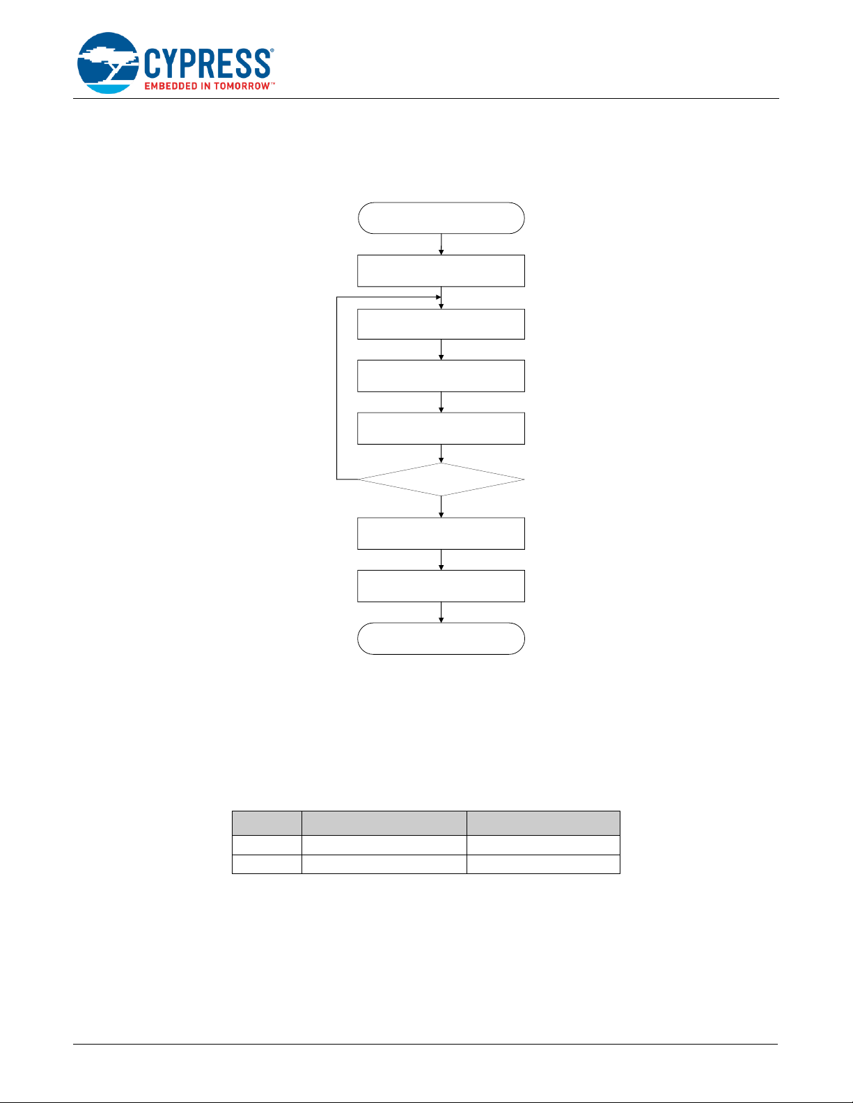
Figure 3 shows how to configure P-DMA and M-DMA.
Figure 3. General Configuration of P-DMA/M-DMA
Start
Disable P-DMA/M-DMA
Configure Channel
Configure Descriptor
Enable P-DMA/M-DMA
End
Enable P-DMA/M-DMA Channel
Enable peripherals for triggering
DMAs
Is setting of all channel
to be used completed ?
Yes
No
In this example, channel, descriptor, and channel enable are configured for each channel. It is also possible to configure
all channels to be used within each step.
A peripheral trigger is required after setting the corresponding DMA channel.
2.1 Disable/Enable P-DMA/M-DMA
P-DMA and M-DMA can be enabled/disabled using the respective bits as shown in Table 2. The default setting after
reset is ‘0’ (Disabled).
Table 2. P-DMA/M-DMA Disable/Enable
DMA Type
Register (Bit)
Description
P-DMA
DW_CTL.ENABLED (bit31)
0: Disable, 1: Enable
M-DMA
DMAC_CTL.ENABLED (bit31)
0: Disable, 1: Enable
2.2 Configure Channel
In this step, P-DMA/M-DMA channel settings such as the channel priority and pointer address of the descriptor
corresponding to the channel are configured.
In addition, in P-DMA, the preemptable function and CRC calculation mode for CRC transfer are configured, if
necessary.
See Section 2.1 for more details
See Section 2.2 for more details
See Section 2.1 for more details
See Section 2.3 for more details
See Section 2.4 for more details
Page 7
How to Use Direct Memory Access (DMA) Controller in Traveo II Family
www.cypress.com Document Number. 002-20191 Rev. *D 6
Table 3 and Table 4 show the registers that are used for configuring a channel in P-DMA and M-DMA, respectively.
The registers corresponding to the channel number are configured. See the Architecture TRM and Registers Technical
Reference Manual (Registers TRM) for more details.
Table 3. Channel Configuration for P-DMA
Register (Bit)
Description
DW_CH_STRUCT_CH_CURR_PTR
Sets the channel current descriptor pointer. Software needs to initialize this
register.
DW_CH_STRUCT_CH_CTL.PREEMPTABLE
(bit11)
Specifies whether the channel is preemptable.
DW_CH_STRUCT_CH_CTL.PRIO (bit9:8)
Sets the channel priority.
DW_CH_STRUCT_CH_IDX.X_IDX (bit7:0)
Sets the X indices of the channel into the current descriptor. Software needs
to initialize this register.
DW_CH_STRUCT_CH_IDX_Y_IDX (bit15:0)
Sets the Y indices of the channel into the current descriptor. Software needs
to initialize this register.
Required only for CRC transfer:
DW_CRC_CTL.DATA_REVERSE (bit0)
Specifies the bit order (MSb or LSb first) in which a data byte is processed.
DW_CRC_CTL.REM_REVERSE (bit8)
Specifies whether the remainder is bit reversed.
DW_CRC_DATA_CTL.DATA_XOR (bit7:0)
Sets the byte mask with which each data byte is XORed. You can choose this
8-bit value randomly.
DW_CRC_POL_CTL.POLYNOMIAL
Sets the CRC polynomial.
DW_CRC_LFSR_CTL.LFSR32
Sets the seed value for CRC calculation.
DW_CRC_REM_CTL.REM_XOR
Sets a mask with which the CRC_LFSR_CTL.LFSR32 register is XORed.
Table 4. Channel Configuration for M-DMA
Register (Bit)
Description
DMAC_CH_CH_CURR_PTR
Sets the channel current descriptor pointer. Software needs to initialize this
register.
DMAC_CH_CH_CTL.PRIO (bit9:8)
Sets the channel priority.
2.3 Configure Descriptor
In this step, the descriptor is configured. The descriptor specifies the DMA channel’s transfer details. A descriptor is
stored in the memory outside DMA and read by the transfer engine. The transfer engine transfers the data according
to the descriptor. The descriptor pointer position for each channel is stored in the descriptor pointer register (see
Section 2.2).
Figure 4 shows the descriptor structure for P-DMA and M-DMA. The P-DMA descriptor consists of six 32-bit words,
while the M-DMA descriptor consists of eight 32-bit words. However, descriptors of both DMAs have similar functions.
Page 8
How to Use Direct Memory Access (DMA) Controller in Traveo II Family
www.cypress.com Document Number. 002-20191 Rev. *D 7
Figure 4. P-DMA/M-DMA Descriptor Structure
Descriptor Control
Descriptor Pointer +00
Source Address
+04
Destination Address
+08
X Loop Control
+0c
Y Loop Control
+10
Descriptor Next Pointer
+14
Descriptor 0
Descriptor Control
Descriptor Pointer +00
Source Address
+04
Destination Address
+08
X Loop Count
+0c
Y Loop Count
+10
+14
Descriptor next pointer
X Loop Control
Y Loop Control
+18
+1c
M-DMA Descriptor
Structure
P-DMA Descriptor
Structure
Configure Descriptor Parameters
▪
Descriptor control: This word describes DMA parameters such as descriptor type, transfer size, trigger-in/out,
and interrupt setting.
▪
Source address and destination address: These words specify the base addresses of the source and
destination locations.
▪
X loop control and X loop count: These words control the loop in 1D transfer or the inner loop in 2D transfer.
The X loop control specifies the increment of the source and destination addresses for each X loop iteration. The
X loop count specifies the number of iterations of the X loop.
▪
Y loop control and Y loop count: These words control the outer loop in 2D transfer. The Y loop control specifies
the increment of the source and destination addresses for each Y loop iteration. The Y loop count specifies the
number of iterations of the Y loop.
▪
Descriptor next pointer: This word specifies the address of the next descriptor. Descriptors can be chained by
storing the descriptor of the next pointer in the current descriptor. The last descriptor in the descriptor list has ‘0’
(NULL) in this word.
See the Architecture TRM and Registers TRM for descriptor details.
The number of descriptor words used varies depending on the descriptor type. A word address is shifted forward if
there is any unused descriptor word.
Page 9
How to Use Direct Memory Access (DMA) Controller in Traveo II Family
www.cypress.com Document Number. 002-20191 Rev. *D 8
2.3.1 Descriptor Type
This section explains the descriptor type, which determines the type of DMA transfer.
P-DMA has four descriptor types, and M-DMA has five descriptor types. The number of descriptor words used varies
depending on the descriptor type. Table 5 shows each descriptor type. In Table 5, the Transfer Example column shows
the outline and pseudocode of each descriptor type. The Using Descriptor column shows the descriptor word used by
the descriptor types in each DMA. Note that a word address is shifted forward if there is any unused descriptor word.
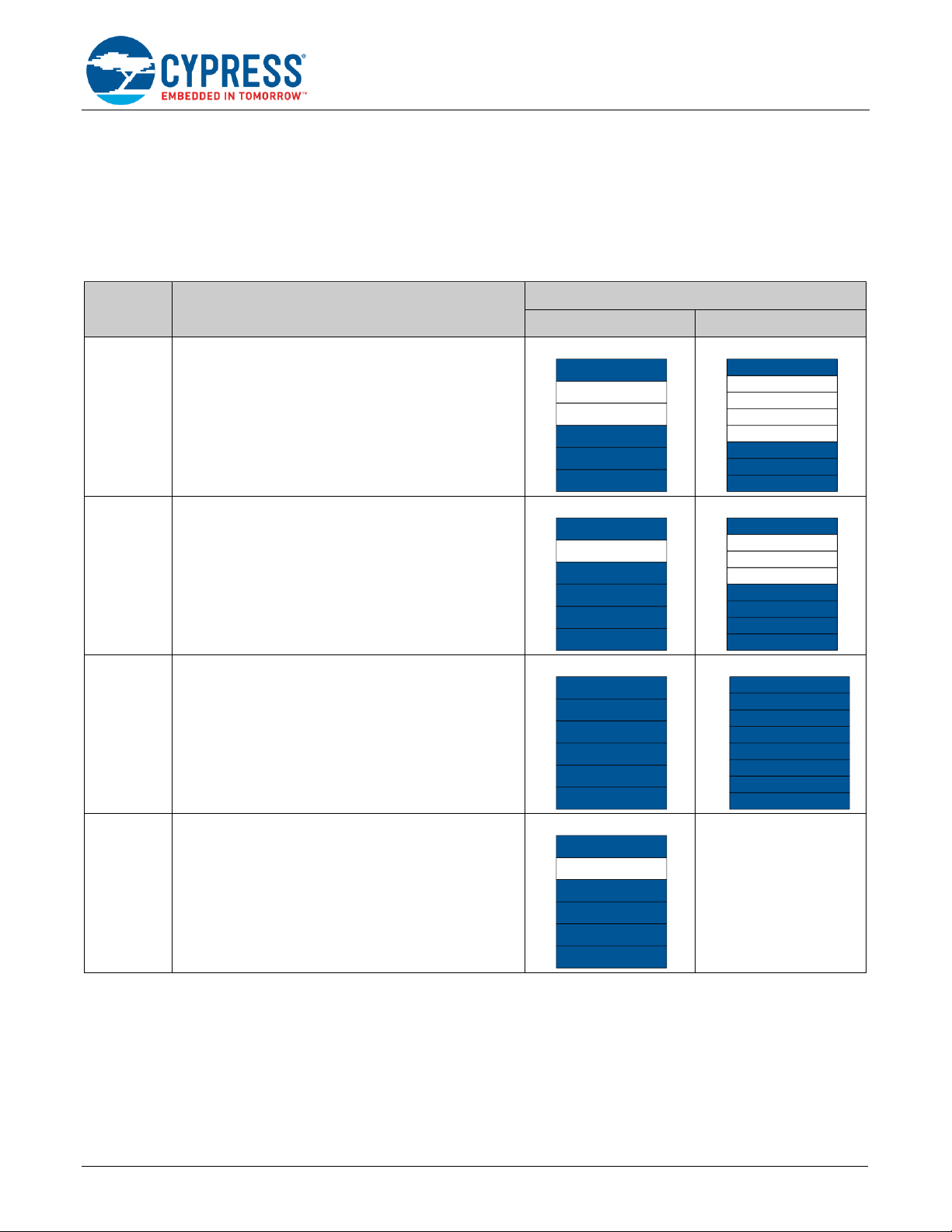
Table 5. P-DMA/M-DMA Transfer Example and Using Descriptor for Each Descriptor Type
Descriptor
Type
Transfer Example
Using Descriptor
P-DMA
M-DMA
Single
transfer
This transfers a single data element:
DST_ADDR = (DATA_SIZE) SRC_ADDR
Descriptor control
+00
Source Address
+04
Destination address
+08
X(Inner) Loop control
Y(Outer) Loop control
Next descriptor pointer
+0c
Descriptor control
+00
Source Address
+04
Destination address
+08
X(Inner) Loop Count
Y(Outer) Loop Count
+0c
Next descriptor pointer
X(Inner) Loop control
Y(Outer) Loop control
1D transfer
One-dimensional “for loop” transfer:
for (X_IDX =0; X_IDX <= COUNT; X_IDX++) {
DST_ADDR[DST_INCR] = (DATA_SIZE)
SRC_ADDR[SRC_INCR]
}
*DST_INCR/SRC_INCR depend on X_INCR DST_ADDR
= (DATA_SIZE) SRC_ADDR
Descriptor control
+00
Source Address
+04
Destination address
+08
X(Inner) Loop control
+0c
Y(Outer) Loop control
+10
Next descriptor pointer
Descriptor control
+00
Source Address
+04
Destination address
+08
X(Inner) Loop Count
+0c
Y(Outer) Loop Count
+10
Next descriptor pointer
X(Inner) Loop control
Y(Outer) Loop control
2D transfer
Two-dimensional “for loop” transfer:
for (Y_IDX =0; Y_IDX <= Y_COUNT; Y_IDX++) {
for (X_IDX =0; X_IDX <= X_COUNT; X_IDX++) {
DST_ADDR[DST_INCR] = (DATA_SIZE)
SRC_ADDR[SRC_INCR]
}
}
*DST_INCR/SRC_INCR depend on X/Y_INCR
Descriptor control
+00
Source Address
+04
Destination address
+08
X(Inner) Loop control
+0c
Y(Outer) Loop control
+14
Next descriptor pointer
+10
Descriptor control
+00
Source Address
+04
Destination address
+08
X(Inner) Loop Count
+0c
Y(Outer) Loop Count
Next descriptor pointer
X(Inner) Loop control
Y(Outer) Loop control
+10
+14
+18
+1c
CRC
transfer
Calculate CRC of the specified area.
Note that for CRC transfer, CRC must be configured with
memory mapped I/O (MMIO) registers.
Descriptor control
+00
Source Address
+04
Destination address
+08
X(Inner) Loop control
+0c
Y(Outer) Loop control
+10
Next descriptor pointer
Not supported
Page 10
How to Use Direct Memory Access (DMA) Controller in Traveo II Family
www.cypress.com Document Number. 002-20191 Rev. *D 9
Descriptor
Type
Transfer Example
Using Descriptor
P-DMA
M-DMA
Memory
copy
One-dimensional “for loop” transfer:
for (X_IDX =0; X_IDX <= X_COUNT; X_IDX+) {
DST_ADDR[IDX] = SRC_ADDR[IDX]
}
Not supported
Descriptor control
+00
Source Address
+04
Destination address
+08
X(Inner) Loop Count
+0c
Y(Outer) Loop Count
+10
Next descriptor pointer
X(Inner) Loop control
Y(Outer) Loop control
Scatter
Write a set of 32-bit data elements, whose addresses are
“scattered” around one-dimensional “for loop” transfer.
for (X_IDX =0; X_IDX <= X_COUNT; X_IDX +=2) {
address = SRC_ADDR[IDX]
data = SRC_ADDR[IDX+1]
*address = data
}
Not supported
Descriptor control
+00
Source Address
+04
Destination address
+08
X(Inner) Loop Count
Y(Outer) Loop Count
+0c
Next descriptor pointer
X(Inner) Loop control
Y(Outer) Loop control
2.3.2 Trigger Functionality
This section explains the trigger function. Trigger input, trigger output (tr_out), and interrupt are controlled by the
descriptor.
A trigger input activates DMA channel transfer. The trigger output (tr_out) and interrupt are output when the transfer is
complete. The trigger operation is specified by TR_IN_TYPE, TR_OUT_TYPE, and INTR_TYPE in the descriptor.
Trigger input, trigger output (tr_out), and interrupt can be configured independently for each channel. See the Registers
TRM for descriptor details.
▪
There are four types of trigger input operations:
Type 0: Trigger results in the execution of a single transfer.
Type 1: Trigger results in the execution of a single 1D transfer.
Type 2: Trigger results in the execution of the current descriptor.
Type 3: Trigger results in the execution of a descriptor list.
▪
There are four types of trigger outputs and interrupt timing:
Type 0: Output trigger or interrupt is generated after a single transfer.
Type 1: Output trigger or interrupt is generated after a single 1D transfer.
Type 2: Output trigger or interrupt is generated after the execution of the current descriptor.
Type 3: Output trigger or interrupt is generated after the execution of a descriptor list.
Page 11

How to Use Direct Memory Access (DMA) Controller in Traveo II Family
www.cypress.com Document Number. 002-20191 Rev. *D 10
2.3.2.1 Examples for Trigger Functionality
This section provides examples for different trigger functions. The descriptor list for the following examples is composed
of chaining two descriptors (Descriptor 0 and Descriptor 1) in a 2D transfer.
Example 1:
This example describes the operation of a Type 0 trigger. Figure 5 shows the operation of the trigger input and trigger
output or interrupt in Type 0 trigger.
Figure 5. Trigger Operation Example 1
||
||
||
Trigger Input
||
||
||
Trigger Output /
Interrupt
Single
Data Transfer
||
||
||
Execute
Single Transfer
Single Single SingleSingle
1D
( =Descriptor 0)
1D
Transfer Status
(1) (2) (7) (8) (16)
(1) (2) (7) (16)(8)
||
||
||
||
||
||
||
||
||
Single
(15)
(15)
2D
When the trigger input is set in Type 0 trigger, P-DMA/M-DMA performs a single transfer with every trigger input.
Therefore, 16 trigger inputs are required to complete Descriptor 0.
When trigger outputs and interrupts are set in Type 0 trigger, the trigger output, interrupt, or both are output each time
a single transfer is completed. Therefore, trigger output, interrupt, or both are output 16 times with the completion of
Descriptor 0.
Example 2:
This example describes the Type 1 trigger operation. Figure 6 shows the operation of trigger input and trigger output
or interrupt in Type 1 trigger.
Figure 6. Trigger Operation Example 2
Execute
1D Transfer
Transfer Status
||
||
||
Trigger Input
||
||
||
Trigger Output /
Interrupt
Single
Data Transfer
||
||
||
Single
(1)
(2)(1)
||
||
||
||
||
||
||
||
||
SingleSingle
(2)
End of 1D End of 1D
1D
( =Descriptor 0)
1D
2D
When trigger input is set in Type 1 trigger, P-DMA/M-DMA performs a 1D transfer with the trigger input. If the next
trigger occurs again, P-DMA/M-DMA performs a 1D transfer. Therefore, two trigger inputs are required to complete
Descriptor 0.
When trigger outputs and interrupts are set in Type 1 trigger, trigger output, interrupt, or both are output each time a
1D transfer is completed. Therefore, trigger output, interrupt, or both are output twice with the completion of Descriptor
0.
Page 12

How to Use Direct Memory Access (DMA) Controller in Traveo II Family
www.cypress.com Document Number. 002-20191 Rev. *D 11
Example 3:
This example describes the operation of Type 2 trigger. Figure 7 shows the operation of the trigger input and trigger
output or interrupt in Type 2 trigger.
Figure 7. Trigger Operation Example 3
||
||
||
Trigger Input
||
||
||
Trigger Output /
Interrupt
Single
Data Transfer
||
||
||
Execute
Descriptor Transfer
Single End of 1D transfer End of Descriptor 1
1D
2D
( =Descriptor 1)
1D
2D
( =Descriptor 0)
Transfer Status
1D
1D
Descriptor chaining
||
||
||
||
||
||
||
||
||
||
||
||
||
||
||
||
||
||
SingleEnd of Descriptor 0 Single
(2)(1)
(1) (2)
When the trigger input is set in Type 2 trigger, P-DMA/M-DMA executes the current descriptor (here: Descriptor 0) with
the trigger input. If the next trigger input occurs, P-DMA/M-DMA executes the next descriptor (here: Descriptor 1).
Therefore, two trigger inputs are required to complete the descriptor list.
When trigger outputs and interrupts are set in Type 2 trigger, trigger output, interrupt, or both are output each time a
current descriptor transfer is completed. Therefore, trigger output, interrupt, or both are output twice with the completion
of the descriptor list.
Example 4:
This example describes the operation of Type 3 trigger. Figure 8 shows the operation of the trigger input and trigger
output or interrupt in Type 3 trigger.
Figure 8. Trigger Operation Example 4
||
||
||
Trigger Input
||
||
||
Trigger Output /
Interrupt
Single
Data Transfer
||
||
||
Execute
Descriptor Transfer
Single End of 1D transfer End of Descriptor 1
1D
2D
( =Descriptor 1)
1D
2D
( =Descriptor 0)
Transfer Status
1D
1D
Descriptor chaining
||
||
||
||
||
||
||
||
||
||
||
||
||
||
||
||
||
||
SingleEnd of Descriptor 0 Single
(1)
(1)
When the trigger input is set in Type 3 trigger, P-DMA/M-DMA executes the complete descriptor list with each trigger
input. Therefore, one trigger input is required to complete the descriptor list.
Page 13

How to Use Direct Memory Access (DMA) Controller in Traveo II Family
www.cypress.com Document Number. 002-20191 Rev. *D 12
When trigger outputs and interrupts are set in Type 3 trigger, the trigger output, interrupt, or both are output when
descriptor list transfer is completed. Therefore, the trigger output and/or interrupt are output once with the completion
of the descriptor list.
2.4 Disable/Enable P-DMA/M-DMA Channel
P-DMA and M-DMA can be configured/programmed to execute multiple independent data transfers. Each data transfer
is managed by a channel.
In DMA channel configuration, the DMA channel must be disabled during the configuration, and enabled after
configuring the channel. Table 6 shows the registers used for enabling or disabling a DMA channel.
The number of channels varies for different part numbers. See the device datasheet for the number of available
channels.
Table 6. Disable/Enable P-DMA/M-DMA Channel
DMA Type
Register (Bit)
Description
P-DMA
DW_CH_STRUCT_CH_CTL.ENABLED (bit31)
0: Disable, 1: Enable
M-DMA
DMAC_CH_CH_CTL.ENABLED (bit31)
0: Disable, 1: Enable
3 P-DMA Use Cases
3.1 1D Transfer (Memory-to-Peripheral)
3.1.1 Overview
This is an example of transferring the transmit data from the memory to TX-FIFO by DMA when using the SCB UART
mode. In this case, the UART uses an 8-bit data frame, and starts the transmission when the data is written to the FIFO.
The number of bytes to be transmitted is 16 and the TX FIFO setting is 128 elements-deep with 8-bit data elements.
See the “Serial Communications Block (SCB)” chapter of the Architecture TRM for more details.
P-DMA starts the transfer with a software trigger from the CPU, and generates an interrupt to the CPU after transferring
all data into the transmit FIFO.
Figure 9 shows the data transfer.
Figure 9. Use Case of a Memory-to-Peripheral (1D Transfer) Using UART in SCB
d0 d1 d2 d3
d4 d5 d6 d7
d12 d13 d14 d15
. . .
P-DMA
(2)
(3)
RAM base address
(4)
(1)
Ch.7
CPU
(5)
Trigger
Multiplexer
(1)
(0)
Descriptor
Descriptor
Pointer
SCB (UART)
Destination
d0d1d2d14
d15
SCB_TX_FIFO_WR
FIFO (128 elements deep x 8 bit)
・・・
16 byte
data transfer
8 bit
16 byte
Transmission
DATA_SIZE: 8-bit DST_SIZE: 8-bitSRC_SIZE: 8-bit
RAM
Source
(0) Configure P-DMA according to Section 3.1.2, and configure the SCB and trigger multiplexer.
(1) CPU notifies a software trigger to P-DMA via the trigger multiplexer.
Page 14

How to Use Direct Memory Access (DMA) Controller in Traveo II Family
www.cypress.com Document Number. 002-20191 Rev. *D 13
(2) P-DMA reads the descriptor from the specified area (Descriptor Pointer) when activating the next pending channel.
(3) P-DMA reads data (d0) from the source address (RAM base address).
(4) P-DMA writes the read data (d0) to the destination address (SCB_TX_FIFO_WR). After that, P-DMA increments
the source address by 0x01, but there is no increment of the destination address. Then, P-DMA reads the data
(d1) from the source address (RAM base address +0x01) and writes it to the destination address
(SCB_TX_FIFO_WR) again. P-DMA repeats from (3) to (4) until d15 data is transferred.
(5) P-DMA notifies the CPU with an interrupt when the transfer of all data is completed.
Initialize the channel registers and set the descriptor as follows:
3.1.2 Initial Configuration of Channel Registers
Perform the initial configuration for P-DMA according to Figure 3.
1. Disable P-DMA
DW_CTL.ENABLED = 0 /* disable */
2. Configure Channel
DW_CH_STRUCT_CH_CURR_PTR = descriptor pointer /* Channel current descriptor pointer */
DW_CH_STRUCT_CH_CTL.PREEMPTABLE = 0 /* Channel is not preemptable */
DW_CH_STRUCT_CH_CTL.PRIO = 0 /* Channel priority is 0 */
DW_CH_STRUCT_CH_IDX.X_IDX = 0 /* Initialize Channel X indices to 0 */
DW_CH_STRUCT_CH_IDX.Y_IDX = 0 /* Initialize Channel Y indices to 0 */
3. Configure Descriptor
DESCR_CTL.WAIT_FOR_DEACT = 0 /* Do not wait for trigger deactivation */
DESCR_CTL.INTR_TYPE = 0 /* Interrupts on every element transfer completion */
DESCR_CTL.TR_OUT_TYPE = 0 /* Triggers on every element transfer completion */
DESCR_CTL.TR_IN_TYPE = 2 /* Transfer the entire descriptor with each trigger */
DESCR_CTL.CH_DISABLE = 1 /* Channel is disabled after the completion of the current
descriptor */
DESCR_CTL.SRC_TRANSFER_SIZE = 0 /* as specified in DATA_SIZE */
DESCR_CTL.DST_TRANSFER_SIZE = 1 /* Word (32-bit) */
DESCR_CTL.DATA_SIZE = 0 /* byte (8-bit) */
DESCR_CTL.DESCR_TYPE = 1 /* 1D transfer */
DESCR_SRC = RAM base address /* Address of stored transfer data in RAM */
DESCR_DST = SCB_TX_FIFO_WR /* Address of writing to FIFO */
DESCR_X_CTL.SRC_X_INCR = 1 /* address +0x01 */
DESCR_X_CTL.DST_X_INCR = 0 /* Not increase */
DESCR_X_CTL.X_COUNT = 15 /* Buffer size is 16 data elements */,
DESCR_NEXT_PTR = 0 /* No descriptor chain */
4. Enable P-DMA Channel
DW_CH_STRUCT_CH_CTL.ENABLED = 1 /* Enable */
5. Enable P-DMA
DW_CTL.ENABLED = 1 /* Enable */
Page 15

How to Use Direct Memory Access (DMA) Controller in Traveo II Family
www.cypress.com Document Number. 002-20191 Rev. *D 14
3.2 1D Transfer (Peripheral-to-Memory)
3.2.1 Overview
This is an example of transferring input states of multiple ports to the memory (RAM) with a periodic trigger. A TCPWM
is used for generating the periodic trigger. See the “Timer, Counter, and PWM” chapter of the Architecture TRM for
more details.
The port input state is stored in the memory with the periodic timing set in TCPWM. As a result, the CPU can know the
port state at a specified time by reading the memory without the CPU having to access the port register. This is useful
when storing the port state before transitioning to a low-power mode.
In this case, P-DMA transfers the GPIO_PRT_IN register data to RAM. The number of registers to be transferred is 23.
(from Port 0 to Port 22). GPIO_PRT_IN registers exist at intervals of 0x80. P-DMA generates an interrupt after data is
transferred from all registers. Figure 10 shows the data transfer.
Figure 10. Operation of 1D Transfer (Peripheral-to-Memory)
PRT0 Status Data
PRT1 Status Data
P-DMA
RAM base address
DATA_SIZE: 32-bit
DST_SIZE: 32-bit
SRC_SIZE: 32-bit
Ch.8
GPIO_PRT0_IN
GPIO_PRT1_IN
GPIO_PRT22_IN
Register
RAM
Trigger
Multiplexer
(2)
TCPWM
CPU
Descriptor
(0)
(0) (1)
(2)
(3)
(4)(4)
(5)
0x80
Descriptor pointer
(6)
RAM base address
+0x04
・
・
PRT22 Status Data
・
・
(0) Configure P-DMA according to Section 3.2.2. In addition, configure the TCPWM and trigger multiplexer.
(1) The CPU starts the TCPWM timer.
(2) TCPWM outputs the trigger to P-DMA via the trigger multiplexer when it reaches the specified count value
(overflow).
(3) P-DMA reads the descriptor from the specified area (Descriptor Pointer) when accepting the transfer.
(4) P-DMA reads the data from the source address (GPIO_PRT0_IN), and writes the read data to the destination
address (RAM base address). After that, P-DMA increments the source address by 0x80 and the destination
address by 0x04. Then, P-DMA reads the data from the source address (GPIO_PRT1_IN) and writes it to the
destination address (RAM base address +0x04) again.
(5) P-DMA notifies the CPU with an interrupt when all transfers are completed.
(6) The CPU accepts the interrupt and reads the port states in the RAM.
When the TCPWM outputs the trigger again, steps (3) to (6) are repeated.
Page 16

How to Use Direct Memory Access (DMA) Controller in Traveo II Family
www.cypress.com Document Number. 002-20191 Rev. *D 15
3.2.2 Initial Configuration for P-DMA
This section describes the initialization of the DMA channel and descriptor. Perform the initial configuration for P-DMA
according to Figure 3.
1. Disable P-DMA
DW_CTL.ENABLED(bit31) = 0 /* Disable */
2. Configure Channel
DW_CH_STRUCT_CH_CURR_PTR = descriptor pointer /* Channel current descriptor pointer */
DW_CH_STRUCT_CH_CTL.PREEMPTABLE = 0 /* Channel is not preemptable */
DW_CH_STRUCT_CH_CTL.PRIO = 0 /* Channel priority is 0 */
DW_CH_STRUCT_CH_IDX.X_IDX = 0 /* Initialize Channel X indices to 0 */
DW_CH_STRUCT_CH_IDX.Y_IDX = 0 /* Initialize Channel Y indices to 0 */
3. Configure Descriptor
DESCR_CTL.WAIT_FOR_DEACT = 0 /* Do not wait for trigger deactivation */
DESCR_CTL.INTR_TYPE = 1 /* Interrupts on the execution of 1D transfer */
DESCR_CTL.TR_OUT_TYPE = 0 /* Not use It must be disabled by the trigger multiplexer*/
DESCR_CTL.TR_IN_TYPE = 2 /* Transfer the entire descriptor per trigger */
DESCR_CTL.CH_DISABLE = 0 /* Not disable after completion of the current descriptor*/
DESCR_CTL.SRC_TRANSFER_SIZE = 0 /* as specified in DATA_SIZE */
DESCR_CTL.DST_TRANSFER_SIZE = 0 /* as specified in DATA_SIZE */
DESCR_CTL.DATA_SIZE = 2 /* Word (32-bit) */
DESCR_CTL.DESCR_TYPE = 1 /* 1D transfer */
DESCR_SRC = GPIO_PRT_IN /* address of the GPIO_PRT_IN */
DESCR_DST = RAM base address /* address of the buffer in memory */
DESCR_X_CTL.SRC_X_INCR = 32 /* address +80h */
DESCR_X_CTL.DST_X_INCR = 1 /* address +04h */
DESCR_X_CTL.X_COUNT = 22 /* 23 data elements */,
DESCR_NEXT_PTR = 0 /* No descriptor chain */
4. Enable P-DMA Channel
DW_CH_STRUCT_CH_CTL.ENABLED = 1 /* Enable */
5. Enable P-DMA
DW_CTL.ENABLED = 1 /* Enable */
3.3 Descriptor Chaining
3.3.1 Overview
This is an example of descriptor chaining by storing the pointer of the next descriptor (DESCR_NEXT_PTR) in the
current descriptor.
This example uses two descriptors: Descriptor 0 and Descriptor 1. Both descriptors are for a 1D transfer that transfers
multiple port input states to the memory (RAM) with a periodic trigger from the TCPWM. However, Descriptor 0 has
RAM base address 0 as the destination address, and Descriptor 1 has RAM base address 1 as the destination address.
P-DMA transfers multiple port input states to the memory (RAM) with a periodic trigger from the TCPWM. P-DMA
notifies the interrupt to the CPU when the transfer is completed. The pointer to the next descriptor
(DESCR_NEXT_PTR) in the descriptor (Descriptor 0) of this transfer is set to a pointer to another descriptor (Descriptor
1). As a result, P-DMA can start the Descriptor 1 transfer when Descriptor 0 transfer completes. Descriptor 0 and
Descriptor 1 have different destination addresses.
P-DMA allows data of the same port address to be transferred to different RAM addresses. In other words, it can have
a double buffer. In this case, Descriptor 0 and Descriptor 1 are chained with each other, and Descriptor 0 and Descriptor
1 have a circular list.
Figure 11 shows 1D transfer with descriptor chaining.
Page 17

How to Use Direct Memory Access (DMA) Controller in Traveo II Family
www.cypress.com Document Number. 002-20191 Rev. *D 16
Figure 11. 1D Transfer with Descriptor Chaining
PRT0 Status Data
PRT1 Status Data
P-DMA
RAM base address 0
Ch.8
PRT22 Status Data
RAM
Trigger
Multiplexer
(2)
TCPWM
CPU
Descriptor 1
(0)
(0) (1)
(2)
(4)
(4)
(5)
Descriptor pointer 0
RAM base address 0
+0x04
Descriptor 0
(3)
Buffer 0
P-DMA
Ch.8
RAM
Trigger
Multiplexer
(6)
TCPWM
CPU
(6)
(8)
(8)
(9)
(7)
Descriptor chaining
GPIO_PRT0_IN
GPIO_PRT1_IN
GPIO_PRT22_IN
Register
0x80
・
・
GPIO_PRT0_IN
GPIO_PRT1_IN
GPIO_PRT22_IN
Register
0x80
・
・
・
・
PRT0 Status Data
PRT1 Status Data
PRT22 Status Data
Buffer 1
・
・
PRT0 Status Data
PRT1 Status Data
PRT22 Status Data
Descriptor 1
Descriptor pointer 1
Descriptor 0
Buffer 0
・
・
PRT0 Status Data
PRT1 Status Data
RAM base address 1
PRT22 Status Data
RAM base address 1
+0x04
Buffer 1
・
・
(0) Configure P-DMA according to the usage example. In addition, configure the TCPWM and trigger multiplexer.
(1) The CPU starts the TCPWM timer.
(2) The TCPWM outputs the trigger to P-DMA via the trigger multiplexer when it reaches the specified count value
(overflow).
(3) P-DMA reads the descriptor from the specified area (Descriptor Pointer 0) when activating the next pending transfer.
Page 18

How to Use Direct Memory Access (DMA) Controller in Traveo II Family
www.cypress.com Document Number. 002-20191 Rev. *D 17
(4) P-DMA reads the data from the source address (GPIO_PRT0_IN), and writes the read data to the destination
address (RAM base address 0). After that, P-DMA increments the source address by 0x80 and the destination
address by 0x04. Then, P-DMA reads the data from the source address (GPIO_PRT1_IN) and writes it to the
destination address (RAM base address 0 +0x04) again.
(5) P-DMA notifies the CPU with an interrupt when all transfers are completed.
(6) The TCPWM outputs the trigger to P-DMA when it reaches the specified count value (overflow) again.
(7) P-DMA reads the descriptor from the pointer defined by the next descriptor pointer in its own descriptor (Descriptor
Pointer 1) when accepting the transfer.
(8) P-DMA reads the data from the source address (GPIO_PRT0_IN), and writes the read data to the destination
address (RAM base address 1). After that, P-DMA increments the source address by 0x80 and the destination
address by 0x04. Then, P-DMA reads the data from the source address (GPIO_PRT1_IN) and writes it to the
destination address (RAM base address 1 +0x04) again.
P-DMA notifies the CPU through an interrupt when all transfers are completed. Descriptor 1 chains to Descriptor 0.
Therefore, when the TCPWM outputs the trigger again, steps from (3) are repeated.
Note: The TCPWM count period must always be longer than the time required by DMA to transfer all data.
3.3.2 Initial Configuration
This section describes the initialization of the DMA channel and descriptor of this use case. Perform the initial
configuration for P-DMA according to Figure 3.
1. Disable P-DMA
DW_CTL.ENABLED = 0 /* Disable */
2. Configure Channel
DW_CH_STRUCT_CH_CURR_PTR = descriptor pointer 0 /* Channel current descriptor pointer */
DW_CH_STRUCT_CH_CTL.PREEMPTABLE = 0 /* Channel is not preemptable */
DW_CH_STRUCT_CH_CTL.PRIO = 0 /* Channel priority is 0 */
DW_CH_STRUCT_CH_IDX.X_IDX = 0 /* Initialize Channel X indices to 0 */
DW_CH_STRUCT_CH_IDX.Y_IDX = 0 /* Initialize Channel Y indices to 0 */
3. Configure Descriptor 0
DESCR_CTL.WAIT_FOR_DEACT = 0 /* Do not wait for trigger deactivation */
DESCR_CTL.INTR_TYPE = 1 /* Interrupts on the execution of 1D transfer */
DESCR_CTL.TR_OUT_TYPE = 0 /* Not use It must be disabled by the trigger
multiplexer*/
DESCR_CTL.TR_IN_TYPE = 2 /* Transfer the entire descriptor per trigger */
DESCR_CTL.CH_DISABLE = 0 /* Not disable */
DESCR_CTL.SRC_TRANSFER_SIZE = 0 /* as specified in DATA_SIZE */
DESCR_CTL.DST_TRANSFER_SIZE = 0 /* as specified in DATA_SIZE */
DESCR_CTL.DATA_SIZE = 2 /* Word (32-bit) */
DESCR_CTL.DESCR_TYPE = 1 /* 1D transfer */
DESCR_SRC = GPIO_PRT_IN /* address of the GPIO_PRT_IN */
DESCR_DST = RAM base address 0 /* address of the buffer 0 in memory */
DESCR_X_CTL.SRC_X_INCR = 32 /* address +80h */
DESCR_X_CTL.DST_X_INCR = 1 /* address +04h */
DESCR_X_CTL.X_COUNT = 22 /* 23 data elements */
DESCR_NEXT_PTR = descriptor pointer 1 /* Descriptor chain to descriptor 1 */
4. Configure Descriptor 1
Configuration of Descriptor 1 is the same as that of Descriptor 0, except for the following:
DESCR_DST = RAM base address 1 /* address of the buffer 1 in memory */
DESCR_NEXT_PTR = descriptor pointer 0 /* Descriptor chain to descriptor 0 */
5. Enable P-DMA Channel
DW_CH_STRUCT_CH_CTL.ENABLED = 1 /* Enable */
6. Enable P-DMA
DW_CTL.ENABLED = 1 /* Enable */
Page 19

How to Use Direct Memory Access (DMA) Controller in Traveo II Family
www.cypress.com Document Number. 002-20191 Rev. *D 18
3.4 2D Transfer (Peripheral-to-Memory)
3.4.1 Overview
This example shows how the result of an ADC group conversion is stored to the memory. See the “SAR ADC” chapter
of the Architecture TRM for more details.
The conversion result is grouped for each channel and stored in the memory. In this example, the ADC converts three
channels CH_0, CH_1, and CH_2 by group conversion at a specified period. P-DMA stores the three group conversion
results in the memory for each channel with the ADC conversion completion trigger.
Figure 12 shows how 2D transfer works.
Figure 12. 2D Transfer (Peripheral-to-Memory)
(0) Configure P-DMA according to the usage example. In addition, configure the ADC and trigger multiplexer.
(1) The CPU starts ADC group conversion.
(2) The ADC outputs the trigger to P-DMA via the trigger multiplexer when group conversion is completed.
(3) P-DMA reads the descriptor from the specified area (Descriptor Pointer) when accepting the transfer.
(4) P-DMA reads the data from the source address (CH_0_RESULT), and writes the read data to the destination
address (RAM base address).
(5) P-DMA increments the source address by 0x40 and the destination address by 0x20. Then, P-DMA reads the data
from the source address (CH_1_RESULT) and writes it to the destination address (RAM base address 0 +0x20).
(6) P-DMA increments the source address by 0x40 and the destination address by 0x20. Then, P-DMA reads the data
from the source address (CH_2_RESULT) and writes it to the destination address (RAM base address 0 +0x40).
When the next trigger occurs, P-DMA increments the RAM base address by 0x04 and repeats from (4).
P-DMA
Ch.8
CH_0_RESULT
CH_1_RESULT
CH_2_RESULT
ADC Register
Trigger
Multiplexer
(2)
CPU
(0)
(0) (1)
(2)
(4)
(4)
(7)
0x40
Descriptor pointer
(3)
CH_0 conversion result 0
CH_0 conversion result 1
CH_0 conversion result 2
RAM
CH_1 conversion result 0
CH_1 conversion result 1
CH_1 conversion result 2
CH_2 conversion result 0
CH_2 conversion result 1
CH_2 conversion result 2
RAM base address
RAM base address
+0x20
RAM base address
+0x40
0x04
Descriptor 0
ADC
(5)
(6)
0x20
Page 20

How to Use Direct Memory Access (DMA) Controller in Traveo II Family
www.cypress.com Document Number. 002-20191 Rev. *D 19
(7) P-DMA notifies the CPU with an interrupt after transferring CH_ 2 conversion result 2.
In this case, three triggers are required for completing the descriptor.
3.4.2 Initial Configuration
This section describes the initialization of the DMA channel and descriptor of this use case. Perform the initial
configuration for P-DMA according to Figure 3.
1. Disable P-DMA
DW_CTL.ENABLED = 0 /* Disable */
2. Configure Channel
DW_CH_STRUCT_CH_CURR_PTR = descriptor pointer /* Channel current descriptor pointer */
DW_CH_STRUCT_CH_CTL.PREEMPTABLE = 0 /* Channel is not preemptable */
DW_CH_STRUCT_CH_CTL.PRIO = 0 /* Channel priority is 0 */
DW_CH_STRUCT_CH_IDX.X_IDX = 0 /* Initialize Channel X indices to 0 */
DW_CH_STRUCT_CH_IDX.Y_IDX = 0 /* Initialize Channel Y indices to 0 */
3. Configure Descriptor 0
DESCR_CTL.WAIT_FOR_DEACT = 0 /* Do not wait for trigger deactivation */
DESCR_CTL.INTR_TYPE = 2 /* Interrupts on the execution of descriptor */
DESCR_CTL.TR_OUT_TYPE = 0 /* Not use It must be disabled by the trigger
multiplexer*/
DESCR_CTL.TR_IN_TYPE = 1 /* Transfer the entire 1D Transfer per trigger */
DESCR_CTL.CH_DISABLE = 0 /* Not disable */
DESCR_CTL.SRC_TRANSFER_SIZE = 0 /* as specified in DATA_SIZE */
DESCR_CTL.DST_TRANSFER_SIZE = 0 /* as specified in DATA_SIZE */
DESCR_CTL.DATA_SIZE = 2 /* Word (32-bit) */
DESCR_CTL.DESCR_TYPE = 2 /* 2D transfer */
DESCR_SRC = CH_0_RESULT /* address of the CH_0_RESULT */
DESCR_DST = RAM base address /* address of the buffer in memory */
DESCR_X_CTL.SRC_X_INCR = 16 /* address +40h */
DESCR_X_CTL.DST_X_INCR = 8 /* address +20h */
DESCR_X_CTL.X_COUNT = 3 /* 3 data elements */
DESCR_Y_CTL.SRC_Y_INCR = 0 /* Not increments */
DESCR_Y_CTL.DST_Y_INCR = 1 /* Destination address + 0x04 */
DESCR_Y_CTL.Y_COUNT = 2 /* Store results for three times */
DESCR_NEXT_PTR = 0 /* No descriptor chain */
4. Enable P-DMA Channel
DW_CH_STRUCT_CH_CTL.ENABLED = 1 /* Enable */
5. Enable P-DMA
DW_CTL.ENABLED = 1 /* Enable */
3.5 CRC Transfer
3.5.1 Overview
This section describes an example of CRC transfer. CRC transfer is a P-DMA-specific descriptor type. CRC transfer
calculates the CRC in the area that is specified by the source address and size, and transfers the result to the
destination address.
This is an example of program code validation in the flash with CRC transfer. The CPU calculates the CRC of the
program code area with P-DMA before program execution. CRC calculation is performed by using CRC32. When the
result of CRC calculation matches the expected value, the CPU starts the execution of the program. In this example,
note that it is necessary to prepare for the expected value of the program code.
See the Architecture TRM for details of CRC parameters that can be set by P-DMA.
Figure 13 shows a use case of a CRC transfer.
Page 21

How to Use Direct Memory Access (DMA) Controller in Traveo II Family
www.cypress.com Document Number. 002-20191 Rev. *D 20
Figure 13. Use Case of CRC Transfer
(0) Configure P-DMA according to the usage example.
(1) CPU notifies a software trigger to P-DMA via the trigger multiplexer.
(2) P-DMA reads the descriptor from the specified area (Descriptor Pointer) when accepting the transfer.
(3) P-DMA reads the data from the source address (code base address).
(4) P-DMA inputs the read data to the CRC calculator, and reads the data again after incrementing the address. P-
DMA repeats (4) until it reaches the area specified by the transfer size (code size).
(5) When CRC calculation of the specified area is completed, the result is transferred to the destination address (RAM
base address).
(6) P-DMA notifies an interrupt to the CPU.
(7) When the CPU accepts an interrupt, it compares the result with the expected value. When it matches, CPU starts
program execution. If it does not match, CPU transfers to safe operation mode.
3.5.2 Initial Configuration
This section describes the initialization of the DMA channel and descriptor of this use case. Perform the initial
configuration for P-DMA according to Figure 3.
1. Disable P-DMA
DW_CTL.ENABLED = 0 /* Disable */
2. Configure Channel
DW_CH_STRUCT_CH_CURR_PTR = Descriptor pointer /* Channel current descriptor pointer */
DW_CH_STRUCT_CH_CTL.PREEMPTABLE = 0 /* Channel is not preemptable */
DW_CH_STRUCT_CH_CTL.PRIO = 0 /* Channel priority is 0 */
DW_CH_STRUCT_CH_IDX.X_IDX = 0 /* Initialize Channel X indices to 0 */
DW_CH_STRUCT_CH_IDX.Y_IDX = 0 /* Initialize Channel Y indices to 0 */
When using CRC transfer, also set the following registers:
DW_CRC_CTL.DATA_REVERSE = 1 /* Least significant bit (bit 0) first */
DW_CRC_CTL.REM_REVERSE = 1 /* remainder is bit reversed */
DW_CRC_DATA_CTL.DATA_XOR = 0 /* each data byte is XORed with 00h */
DW_CRC_POL_CTL.POLYNOMINAL = 0x04c11db7 /* CRC32: POLYNOMIAL */
DW_CRC_LFSR_CTL.LFSR32 = 0xFFFFFFFF /* seed value */
DW_CRC_REM_CTL.REM_XOR = 0xFFFFFFFF /* CRC_LFSR_CTL.LFSR32 register is XORed
with FFFFh */
RAM
Destination
P-DMA
(2)
Result
CRC
calculation
(3)
(4)
FLASH
Source
Code Area
Code base address
Code size
RAM base addressDATA_SIZE: 32-bit
DST_SIZE: 32-bit
(5)
(1)
Ch.0
SRC_SIZE: 32-bit
CPU
(6)
Trigger
Multiplexer
(1)
(0)
Descriptor
Descriptor
Pointer
(7)
Page 22

How to Use Direct Memory Access (DMA) Controller in Traveo II Family
www.cypress.com Document Number. 002-20191 Rev. *D 21
3. Configure Descriptor
DESCR_CTL.WAIT_FOR_DEACT = 0 /* Do not wait for trigger deactivation */
DESCR_CTL.INTR_TYPE = 0 /* Interrupts on every element transfer
completion */
DESCR_CTL.TR_OUT_TYPE = 0 /* Not use It must be disabled by the trigger
multiplexer*/
DESCR_CTL.TR_IN_TYPE = 2 /* Descriptor is 1D transferred per trigger */
DESCR_CTL.CH_DISABLE = 1 /* Channel is disabled after the completion of
the current descriptor */
DESCR_CTL.SRC_TRANSFER_SIZE = 0 /* as specified in DATA_SIZE */
DESCR_CTL.DST_TRANSFER_SIZE = 0 /* as specified in DATA_SIZE */
DESCR_CTL.DATA_SIZE = 2 /* Word (32-bit) */
DESCR_CTL.DESCR_TYPE = 3 /* CRC_TRANSFER */
DESCR_SRC = Code base address /* Program base address in FLASH */
DESCR_DST = RAM base address /* Address of Stored result of calculation */
DESCR_X_CTL.SRC_X_INCR = 1 /* address +1 */
DESCR_X_CTL.DST_X_INCR = 0 /* Not used for CRC transfer */
DESCR_X_CTL.X_COUNT = (Code size/4)-1 /* Depends on CODE_SIZE */
DESCR_NEXT_PTR = 0 /* No descriptor chain */
4. Enable P-DMA Channel
DW_CH_STRUCT_CH_CTL.ENABLED = 1 /* Enable */
5. Enable P-DMA
DW_CTL.ENABLED = 1 /* Enable */
4 M-DMA Use Case
4.1 Memory-to-Memory (Memory Copy)
This section describes an example of memory copy. Memory copy is an M-DMA-specific descriptor type. This is a
special 1D transfer. Memory copy transfer data from the area specified by the source address and size to the destination
address.
This is an example of data transfer from flash to RAM. This descriptor type is useful for copying the program code for
RAM execution and copying the vector table. In the memory copy example, consecutive flash memory areas are
transferred to RAM.
Figure 14 shows a use case of memory-to-memory transfer using memory copy.
Figure 14. Use Case of Memory-to-Memory Using Memory Copy
RAM
Destination
M-DMA
(2)
Copy
Code Area
(3)
FLASH
Source
Source
Code Area
Code base address
Code size
RAM base address
(4)
(1)
Ch.0
CPU
(5)
Trigger
Multiplexer
(1)
(0)
Descriptor
Descriptor
Pointer
Page 23

How to Use Direct Memory Access (DMA) Controller in Traveo II Family
www.cypress.com Document Number. 002-20191 Rev. *D 22
(0) Set M-DMA according to the usage example setting.
(1) CPU notifies a software trigger to M-DMA via the trigger multiplexer.
(2) M-DMA reads the descriptor from the specified area (Descriptor Pointer) when accepting the transfer.
(3) M-DMA reads the data from the source address (code base address).
(4) M-DMA writes the read data to the destination address (RAM base address). After that, increment the source
address and destination address. M-DMA repeats (3) (4) until it reaches the area specified by the transfer size
(code size).
(5) When memory copy of the specified area is completed, M-DMA notifies an interrupt to CPU.
4.1.1 Initial Configuration
This section describes the initialization of the DMA channel and descriptor of this use case. Perform the initial
configuration for M-DMA according to Figure 3.
1. Disable M-DMA
DMAC_CTL.ENABLED = 0 /* Disable */
2. Configure Channel
DMAC_CH_CH_CURR_PTR = Descriptor pointer /* Channel current descriptor pointer */
DMAC_CH_CH_CTL.PRIO = 0 /* Channel priority is 0 */
3. Configure Descriptor
DESCR_CTL.WAIT_FOR_DEACT = 0 /* Do not wait for trigger deactivation */
DESCR_CTL.INTR_TYPE = 1 /* Interrupts on the execution of 1D transfer */
DESCR_CTL.TR_OUT_TYPE = 1 /* Not use It must be disabled by the trigger
multiplexer*/
DESCR_CTL.TR_IN_TYPE = 1 /* Descriptor is 1D transferred per trigger */
DESCR_CTL.CH_DISABLE = 1 /* Channel is disabled after the completion of the
current descriptor */
DESCR_CTL.SRC_TRANSFER_SIZE = 0 /* not used */
DESCR_CTL.DST_TRANSFER_SIZE = 0 /* not used */
DESCR_CTL.DATA_SIZE = 0 /* not used */
DESCR_CTL.DESCR_TYPE = 3 /* memory copy */
DESCR_SRC = Code base address /* Copy source address */
DESCR_DST = RAM base address /* Copy destination address */
DESCR_X_CTL.X_COUNT = Code size -1 /* Depends on COPY_SIZE */
DESCR_NEXT_PTR = 0 /* No descriptor chain */
4. Enable M-DMA Channel
DMAC_CH_CH_CTL.ENABLED = 1 /* Enable */
5. Enable M-DMA
DMAC_CTL.ENABLED = 1 /* Enable */
Page 24

How to Use Direct Memory Access (DMA) Controller in Traveo II Family
www.cypress.com Document Number. 002-20191 Rev. *D 23
5 Glossary
Table 7. Glossary
Terms
Description
DMA controller
Direct memory access controller
P-DMA
Peripheral DMA
M-DMA
Memory DMA
Single transfer
This transfers a single data element (8-bit, 16-bit, or 32-bit). See the “Descriptors” section in the Direct Memory
Access chapter of the Architecture TRM for details.
1D transfer
This performs a one-dimensional "for loop" (described in C). See the “Descriptors” section in the Direct Memory
Access chapter of the Architecture TRM for details.
2D transfer
This performs a two-dimensional "for loop" (described in C). See the “Descriptors” section in the Direct Memory
Access chapter of the Architecture TRM for details.
CRC transfer
This performs a one-dimensional “for loop” similar to the 1D transfer. However, the source data is not transferred to
a destination. A CRC is calculated over the source data. Only P-DMA is supported. See the “Descriptors” section in
the Direct Memory Access chapter of the Architecture TRM for details.
Memory copy
This is a special case of 1D transfer. Only M-DMA is supported. See the “Descriptors” section in the Direct Memory
Access chapter of the Architecture TRM for details.
Scatter
This descriptor type is intended to write a set of 32-bit data elements, whose addresses are “scattered” around the
address space. Only M-DMA is supported. See the “Descriptors” section in the Direct Memory Access chapter of
the Architecture TRM for details.
Descriptor
A descriptor specifies the details of data transfer of DMA channels. See the “Descriptors” section in the Direct
Memory Access chapter of the Architecture TRM for details.
Descriptor chain
A DMA channel executes the next descriptor specified in the current descriptor when it completes executing the
descriptor. See the “Descriptors” section in the Direct Memory Access chapter of the Architecture TRM for details.
Descriptor list
Same as descriptor chain.
Descriptor pointer
The start address of the memory where the descriptor is stored. See the “Descriptors” section in the Direct Memory
Access chapter of the Architecture TRM for details.
Descriptor type
The transfer operation type performed by DMA. See the “Descriptors” section in the Direct Memory Access chapter
of the Architecture TRM for details.
Descriptor word
The composition element of the descriptor. There are descriptor control, source/destination address, X/Y loop
control, and descriptor next pointer. See the “P-DMA Descriptor Structure” and “M-DMA Descriptor Structure”
section in the Direct Memory Access chapter of the Architecture TRM for details.
Preemptable
P-DMA specific functions. See the “Channels” section in the Direct Memory Access chapter of the Architecture
TRM for details.
MMIO
Memory Mapped I/O
ADC
Analog-to-digital converter. See the “SAR ADC” chapter of the Architecture TRM for details.
SCB
Serial Communications Block. See the “Serial Communications Block (SCB)” chapter of the Architecture TRM for
details.
TCPWM
Timer, Counter, and Pulse Width Modulator. See the “Timer, Counter, and PWM” chapter of the Architecture TRM
for details.
Trigger multiplexer
A trigger multiplexer routes triggers from a source peripheral to a destination. See the “Trigger Multiplexer” chapter
of the Architecture TRM for details.
Page 25

How to Use Direct Memory Access (DMA) Controller in Traveo II Family
www.cypress.com Document Number. 002-20191 Rev. *D 24
6 Related Documents
The following are the Traveo II family series datasheets and Technical Reference Manuals. Contact Technical Support
to obtain these documents.
▪
Device datasheet
CYT2B7 Datasheet 32-Bit Arm® Cortex®-M4F Microcontroller Traveo™ II Family
CYT2B9 Datasheet 32-Bit Arm® Cortex®-M4F Microcontroller Traveo™ II Family
CYT4BF Datasheet 32-Bit Arm® Cortex®-M7 Microcontroller Traveo™ II Family
CYT4DN Datasheet 32-Bit Arm® Cortex®-M7 Microcontroller Traveo™ II Family
CYT3BB/4BB Datasheet 32-Bit Arm® Cortex®-M7 Microcontroller Traveo™ II Family
▪
Body Controller Entry Family
Traveo™ II Automotive Body Controller Entry Family Architecture Technical Reference Manual (TRM)
Traveo™ II Automotive Body Controller Entry Registers Technical Reference Manual (TRM) for CYT2B7
Traveo™ II Automotive Body Controller Entry Registers Technical Reference Manual (TRM) for CYT2B9
▪
Body Controller High Family
Traveo™ II Automotive Body Controller High Family Architecture Technical Reference Manual (TRM)
Traveo™ II Automotive Body Controller High Registers Technical Reference Manual (TRM) for CYT4BF
Traveo™ II Automotive Body Controller High Registers Technical Reference Manual (TRM) for CYT3BB/4BB
▪
Cluster 2D Family
Traveo™ II Automotive Cluster 2D Family Architecture Technical Reference Manual (TRM)
Traveo™ II Automotive Cluster 2D Registers Technical Reference Manual (TRM)
Page 26

How to Use Direct Memory Access (DMA) Controller in Traveo II Family
Revision
ECN
Submission
Date
Description of Change
**
6096844
09/06/2018
New application note.
*A
6403271
12/06/2018
Changed target part number from CYT2B5/B7 to CYT2B.
*B
6521580
03/26/2019
Added target parts number (CYT4B series).
Correction of errors in CRC register name.
*C
6688929
10/02/2019
Added target parts number (CYT4D series)
Added the setting flow of DW_CH_STRUCT_CH_IDX into Channel Configuration for P-DMA
*D
6827913
Changed target parts number (CYT2/ CYT4 series).
Added target parts number (CYT3 series).
Document History
Document Title: AN220191 – How to Use Direct Memory Access (DMA) Controller in Traveo II Family
Document Number: 002-20191
03/19/2020
www.cypress.com Document Number. 002-20191 Rev. *D 25
Page 27

How to Use Direct Memory Access (DMA) Controller in Traveo II Family
www.cypress.com Document Number. 002-20191 Rev. *D 26
Worldwide Sales and Design Support
Cypress maintains a worldwide network of offices, solution centers, manufacturer’s representatives, and distributors. To find the
office closest to you, visit us at Cypress Locations.
Products
Arm® Cortex® Microcontrollers
cypress.com/arm
Automotive
cypress.com/automotive
Clocks & Buffers
cypress.com/clocks
Interface
cypress.com/interface
Internet of Things
cypress.com/iot
Memory
cypress.com/memory
Microcontrollers
cypress.com/mcu
PSoC
cypress.com/psoc
Power Management ICs
cypress.com/pmic
Touch Sensing
cypress.com/touch
USB Controllers
cypress.com/usb
Wireless Connectivity
cypress.com/wireless
PSoC® Solutions
PSoC 1 | PSoC 3 | PSoC 4 | PSoC 5LP | PSoC 6 MCU
Cypress Developer Community
Community | Code Examples | Projects | Videos | Blogs |
Training | Components
Technical Support
cypress.com/support
All other trademarks or registered trademarks referenced herein are the property of their respective owners.
© Cypress Semiconductor Corporation, 2018-2020. This document is the property of Cypress Semiconductor Corporation and its subsidiaries (“Cypress”). This
document, including any software or firmware included or referenced in this document (“Software”), is owned by Cypress under the intellectual property laws and
treaties of the United States and other countries worldwide. Cypress reserves all rights under such laws and treaties and does not, except as specifically stated in
this paragraph, grant any license under its patents, copyrights, trademarks, or other intellectual property rights. If the Software is not accompanied by a license
agreement and you do not otherwise have a written agreement with Cypress governing the use of the Software, then Cypress hereby grants you a personal, nonexclusive, nontransferable license (without the right to sublicense) (1) under its copyright rights in the Software (a) for Software provided in source code form, to
modify and reproduce the Software solely for use with Cypress hardware products, only internally within your organization, and (b) to distribute the Software in binary
code form externally to end users (either directly or indirectly through resellers and distributors), solely for use on Cypress hardware product units, and (2) under
those claims of Cypress’s patents that are infringed by the Software (as provided by Cypress, unmodified) to make, use, distribute, and import the Software solely
for use with Cypress hardware products. Any other use, reproduction, modification, translation, or compilation of the Software is prohibited.
TO THE EXTENT PERMITTED BY APPLICABLE LAW, CYPRESS MAKES NO WARRANTY OF ANY KIND, EXPRESS OR IMPLIED, WITH REGARD TO THIS
DOCUMENT OR ANY SOFTWARE OR ACCOMPANYING HARDWARE, INCLUDING, BUT NOT LIMITED TO, THE IMPLIED WARRANTIES OF
MERCHANTABILITY AND FITNESS FOR A PARTICULAR PURPOSE. No computing device can be absolutely secure. Therefore, despite security measures
implemented in Cypress hardware or software products, Cypress shall have no liability arising out of any security breach, such as unauthorized access to or use of
a Cypress product. CYPRESS DOES NOT REPRESENT, WARRANT, OR GUARANTEE THAT CYPRESS PRODUCTS, OR SYSTEMS CREATED USING
CYPRESS PRODUCTS, WILL BE FREE FROM CORRUPTION, ATTACK, VIRUSES, INTERFERENCE, HACKING, DATA LOSS OR THEFT, OR OTHER
SECURITY INTRUSION (collectively, “Security Breach”). Cypress disclaims any liability relating to any Security Breach, and you shall and hereby do release
Cypress from any claim, damage, or other liability arising from any Security Breach. In addition, the products described in these materials may contain design
defects or errors known as errata which may cause the product to deviate from published specifications. To the extent permitted by applicable law, Cypress reserves
the right to make changes to this document without further notice. Cypress does not assume any liability arising out of the application or use of any product or circuit
described in this document. Any information provided in this document, including any sample design information or programming code, is provided only for reference
purposes. It is the responsibility of the user of this document to properly design, program, and test the functionality and safety of any application made of this
information and any resulting product. “High-Risk Device” means any device or system whose failure could cause personal injury, death, or property damage.
Examples of High-Risk Devices are weapons, nuclear installations, surgical implants, and other medical devices. “Critical Component” means any component of a
High-Risk Device whose failure to perform can be reasonably expected to cause, directly or indirectly, the failure of the High-Risk Device, or to affect its safety or
effectiveness. Cypress is not liable, in whole or in part, and you shall and hereby do release Cypress from any claim, damage, or other liability arising from any use
of a Cypress product as a Critical Component in a High-Risk Device. You shall indemnify and hold Cypress, its directors, officers, employees, agents, affiliates,
distributors, and assigns harmless from and against all claims, costs, damages, and expenses, arising out of any claim, including claims for product liability, personal
injury or death, or property damage arising from any use of a Cypress product as a Critical Component in a High-Risk Device. Cypress products are not intended
or authorized for use as a Critical Component in any High-Risk Device except to the limited extent that (i) Cypress’s published data sheet for the product explicitly
states Cypress has qualified the product for use in a specific High-Risk Device, or (ii) Cypress has given you advance written authorization to use the product as a
Critical Component in the specific High-Risk Device and you have signed a separate indemnification agreement.
Cypress, the Cypress logo, Spansion, the Spansion logo, and combinations thereof, WICED, PSoC, CapSense, EZ-USB, F-RAM, and Traveo are trademarks or
registered trademarks of Cypress in the United States and other countries. For a more complete list of Cypress trademarks, visit cypress.com. Other names and
brands may be claimed as property of their respective owners.
 Loading...