

Page 1

Please note that Cypress is an Infineon Technologies Company.
The document following this cover page is marked as “Cypress” document as this is the
company that originally developed the product. Please note that Infineon will continue
to oer the product to new and existing customers as part of the Infineon product
portfolio.
Continuity of document content
The fact that Infineon oers the following product as part of the Infineon product
portfolio does not lead to any changes to this document. Future revisions will occur
when appropriate, and any changes will be set out on the document history page.
Continuity of ordering part numbers
Infineon continues to support existing part numbers. Please continue to use the
ordering part numbers listed in the datasheet for ordering.
www.infineon.com
Page 2
www.cypress.com Document Number: 002-20152 Rev. *C 1
AN220152
How to Retain RAM Data in Reset Procedure and Low-Power Mode Transition in
Traveo II Family
Author: Masahide Karino
Associated Part Family: Traveo™ II Family CYT2/CYT3/CYT4 Series
Related Documents: see Related Documents
AN220152 explains the procedure to ensure RAM retention in Traveo™ II Family MCU when a software reset or lowpower mode transition occurs.
1 Introduction
This application note describes the procedure for reset and low-power mode transitions in Cypress Traveo II family
CYT2/CYT3/CYT4 series devices to ensure RAM retention.
In these devices, a reset is performed asynchronously regardless of the RAM access status. Thus, if a reset occurs
during operation, the RAM data might be lost. In addition, if the device power mode transitions from active to low-power,
you should follow the appropriate procedure for RAM retention. This document describes the procedures to ensure
RAM data retention after a software reset or low-power mode transition. However, in Hibernate mode, the RAM data
cannot be retained. Therefore, the RAM data should be transferred to the application flash once. After returning to
Active mode, it is necessary to return the RAM data from the application flash to RAM. In this case, the transition data
is defined as backup memory data.
To understand the functionality described and terminology used in this application note, refer to the “SRAM
Interface” and “Work Flash” chapter of the Architecture Technical Reference Manual (TRM).
2 RAM Retention Procedure Overview
2.1 Reset Procedure
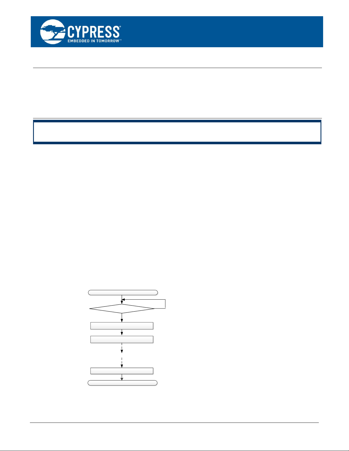
Figure 1 shows the flow of RAM retention when a reset occurs. This example shows the case of retaining RAM0 data.
Figure 1. Example of RAM0 Retention Procedure
Start
End
CPUSS_RAM0_PWR_MACRO_CTLx
- PWR_MODE: RETAINED
CPUSS_RAM0_STATUS
- WB_EMPTY: Wait until the WB_EMPTY bit becomes ’1'
'0': Write buffer NOT empty.
'1': Write buffer empty.
Set RETAINED Mode
Write Buffer Empty?
No
Yes
Check BOD
Check BOD reset cause
- SRSS_RES_CAUSE: RESET_BODVDDD
Set Software Reset
Reset release
Set software reset
- CM0P_SCS_AIRCR.SYSRESETREQ=‘1’
First, in the case of RAM0, check the write buffer status of the WB_EMPTY bit of the CPUSS_RAM0_STATUS register.
The WB_EMPTY bit indicates whether there is any data in the write buffer or it is empty.
Page 3
How to Retain RAM Data with Software Reset and Low-Power Mode Transition in Traveo II Family
www.cypress.com Document Number: 002-20152 Rev. *C 2
In CYT2 series MCU, ECC is added to the 32-bit data. Thus, if a partial AHB-Lite writing (8-bit/16-bit) occurs to the
RAM, the missing data is read from the RAM. Then, the missing data and partial write data are merged to generate the
32-bit complete data. ECC is calculated over the 32-bit complete data, and written to the RAM with the 32-bit data. The
CYT3/CYT4 series MCUs have the AXI bus interface. ECC of AXI bus interface is added to the 64-bit data. Therefore,
when a partial writing (8-bit/16-bit/32-bit) occurs to the RAM, the missing data is read from the RAM. Then, the missing
data and partial write data are merged to generate the 64-bit complete data. ECC is calculated over the 64-bit complete
data.
The write buffer is used in this operation. Therefore, there is a possibility that write buffer has data that is not yet written
to the RAM. To prevent missing of unwritten data in the write buffer, it is necessary to check the status of the write
buffer.
If there is valid data, wait until it is written to RAM0. When there is no valid data in the write buffer, set the PWR_MODE
bit of the CPUSS_RAM0_PWR_MACRO_CTLx register to RETAINED mode. Finally, generate a software reset. By
performing such a procedure, it is possible to retain the RAM0 data and execute a reset. However, note that the RAM0
data cannot be retained if the voltage is lower than the Brown-Out Detection (BOD: 2.7 V) level. Therefore, it is the
necessary to confirm that BOD has not occurred after returning from a reset.
Table 1 shows the RAM0 status register. It is necessary to confirm that the WB_EMPTY bit is set to '1' before initiating
a software reset.
Table 1. RAM0 Status Register
Register
Bit Field
Bit
Value
Description
CPUSS_RAM0_STATUS
WB_EMPTY [0]
0
Write buffer not empty.
1
Write buffer empty.
Table 2 shows the Power Control register, which controls system RAM0 power states with a single macro.
Table 2. Power Control Register
Register
Bit Field
Bit
Value
Description
CPUSS_RAM0_PWR_MACRO_CTLx
*PWR_MODE [1:0]
0
OFF mode: Turn OFF the SRAM. This will turn OFF both
array and periphery power of the SRAM; SRAM memory
contents are lost.
1
Reserved
2
RETAINED mode: Keep the SRAM in Retained mode. This
will turn OFF the SRAM periphery power, but array power is
ON to retain memory contents. SRAM contents will be
retained in DeepSleep system power mode.
3
ENABLE mode: Enable the SRAM for regular operation.
SRAM contents will be retained in DeepSleep system power
mode. (Default)
* To set the PWR_MODE bit field, use word access in the CPUSS_RAM0_PWR_MACRO_CTLx register. See the
Registers TRM for details.
This register is for the CPUSS system’s RAM0 controller. This information is used when the RAM0 RETAINED mode
is set.
Page 4
How to Retain RAM Data with Software Reset and Low-Power Mode Transition in Traveo II Family
www.cypress.com Document Number: 002-20152 Rev. *C 3
2.2 Low-Power Mode (DeepSleep Mode) Transition Procedure
Figure 1 shows the flow of RAM retention for low-power mode transition. In this method, when transitioning to a low-
power mode, settings for RAM retention are performed. The procedure to check the status of the Write Buffer and the
RETAINED mode setting of RAM is the same. When the MCU enters a low-power mode, the main program execution
stops. If a wakeup interrupt is generated, the MCU returns to Active mode.
Figure 2. Example of RAM0 Retention Procedure for Low-Power Mode
Start
End
CPUSS_RAM0_PWR_MACRO_CTLx
- PWR_MODE: RETAINED
CPUSS_RAM0_STATUS
- WB_EMPTY: Wait until the WB_EMPTY bit becomes ’1'
'0': Write buffer NOT empty.
'1': Write buffer empty.
Set RETAINED Mode
Write Buffer Empty?
No
Yes
Active mode
Low Power mode
Interrupt
Low power mode
transition
Active mode
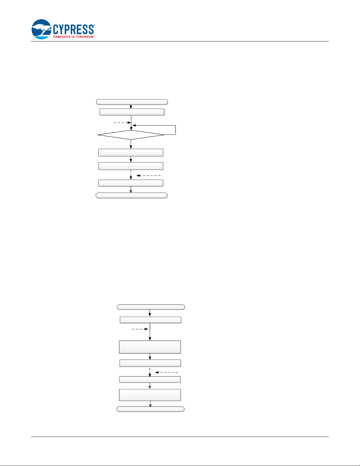
2.3 Low-Power Mode (Hibernate Mode) Transition Procedure
Figure 1 shows how the backup memory data for is backed up for Hibernate mode transition. In this method, when
transitioning to Hibernate mode, the backup memory data of the RAM is transferred to the application flash. When the
MCU enters Hibernate mode, the main program execution stops. If a Hdibernate wakeup reset is generated, the MCU
returns to active mode, and the backup memory data is transferred to the RAM from the application flash. The transfer
of data from the RAM to application flash and back are handled by the user software.
To prevent unintentional overwriting of the backup data, you should consider not allowing other programs to access the
backup data area of the application flash and RAM during data backup. In addition, you should ensure that the data
transition time between the RAM and application flash meets your system requirements.
Figure 3. Example of Backup Procedure for Hibernate Mode
Start
End
Transfer data from RAM
to application flash
Active mode
Hibernate mode
Hibernate Wakeup
Hibernate mode
transition (*)
Active mode
Transfer data from application
flash to RAM
Read RAM data and
write to application
flash
Read application
flash and write to
RAM
Note: (*) Hibernate mode transition
is handled by the user software
Page 5
How to Retain RAM Data with Software Reset and Low-Power Mode Transition in Traveo II Family
www.cypress.com Document Number: 002-20152 Rev. *C 4
3 RAM Retention Procedure in Reset
This section shows two examples for reset procedure with a block diagram, timing chart, and flowchart. One method
uses the Low-Voltage Detection (LVD) interrupt. The other method uses the external reset input signal of the external
LVD IC.
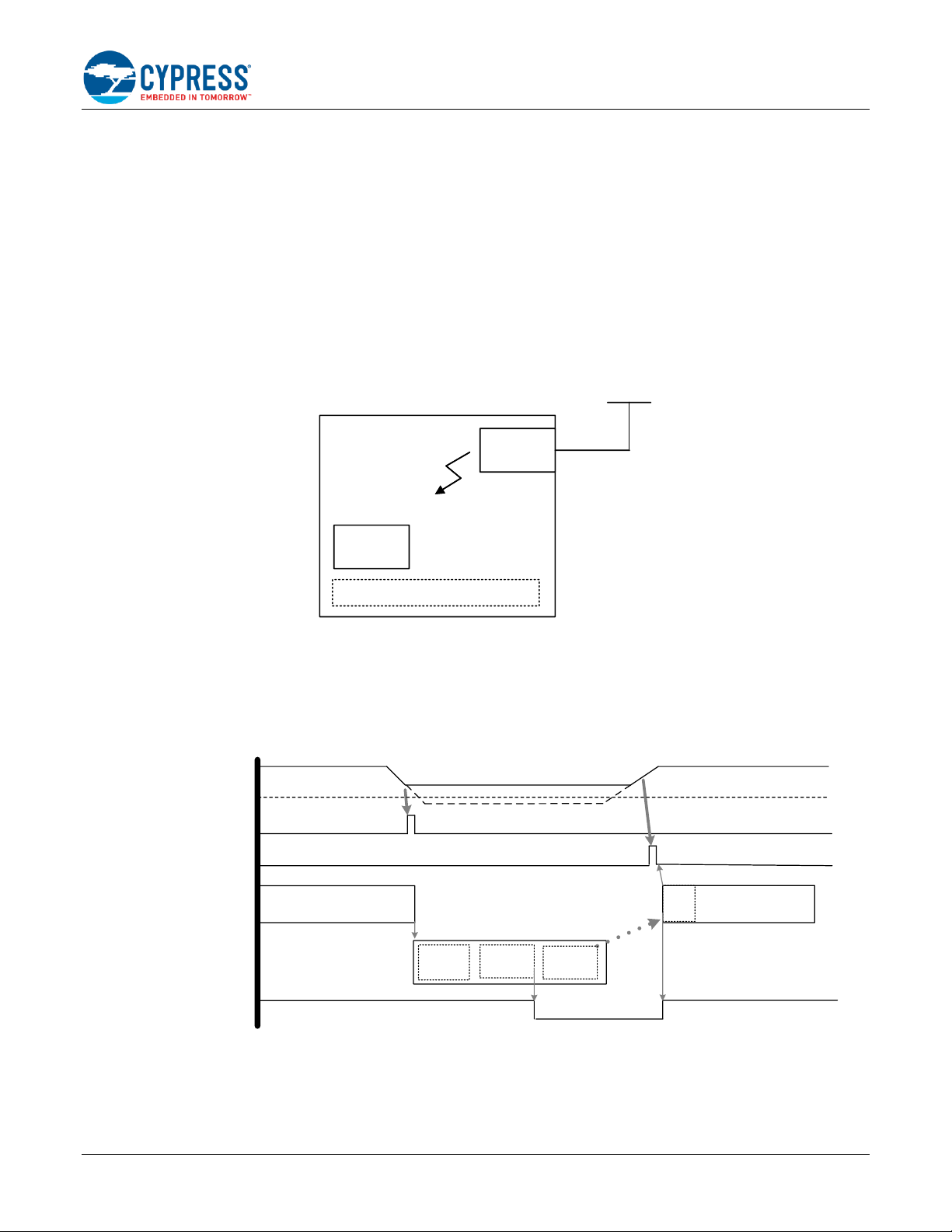
3.1 Reset Using LVD Interrupt
In this case, LVD1 and LVD2 are used. LVD1 is a system low-level voltage detector that ensures that a reset occurs
with guaranteed RAM0 retention. Also, LVD1 is used to detect a VDDD supply voltage drop. In addition, the user
application starts by checking LVD2. LVD2 is used to check whether the VDDD supply voltage has recovered by setting
the rising trip point.
Figure 3. Block Diagram for Reset Procedure for RAM0 Retention with the LVD Interrupt Method
MCU
Software Reset Generation
LVD1,
LVD2
Low Voltage
Detection
RAM0
Retain Mode Setting
Interrupt
5 V
In Figure 3, first, an interrupt is generated when a falling edge is detected from LVD1. After the interrupt has occurred,
RAM0 status needs to be checked and set to RETAINED mode. After these steps, perform a software reset. Then,
after the MCU starts up from reset, check for VDDD exceeding the LVD2 rising edge with the SRSS_INTR register.
Finally, confirm that a BOD reset has not occurred. If a BOD reset occurred, RAM0 data retention is not guaranteed.
Therefore, RAM0 data must be discarded.
Figure 4. Example of Reset Procedure Timing Chart in RAM0 by LVD Interrupt
Interrupt Routine
Interrupt Signal (LVD1)
Main Routine
Interrupt
Normal Operation
Retain
Mode
Setting
Reset
Normal Operation
RAM0 state
Retain Mode
Enable Mode
Restart
RAM
Status
Check
Software
Reset
Setting
Enable Mode
Power Supply (VDDD)
LVD1 Falling
Edge Detection
VDDD
rising
check
LVD2 Rising
Edge Detection
Interrupt
Interrupt Signal (LVD2)
●
●
BOD
●
Not Retain
BOD detection level
In Figure 4, when the VDDD drops, the interrupt routine is called. Then, the interrupt routine checks the RAM0 status,
RETAINED mode setting, and software reset setting (reset generation). After the reset is completed, ensure that VDDD
is rising with the LVD2 detection method, and resume normal operation.
Page 6

How to Retain RAM Data with Software Reset and Low-Power Mode Transition in Traveo II Family
www.cypress.com Document Number: 002-20152 Rev. *C 5
Figure 5. Flowchart of Example Reset Procedure in RAM0 with LVD Interrupt
start
Set RETAINED Mode
Set RETAINED Mode
CPUSS_RAM0_PWR_MACRO_CTL.PWR_MODE=’2'
Check RAM status and wait until the
WB_EMPTY bit becomes ‘1'.
CPUSS_RAM0_STATUS.WB_EMPTY=’1'
Set Software Reset
Set Software Reset
CM0P_SCS_AIRCR.SYSRESETREQ=‘1’
Write Buffer Empty?
No
Yes
Set LVD1,LVD2 Interrupt*
Normal Operation
LVD1
Interrupt
Reset
End
BOD Reset Check
Check BOD reset cause
SRSS_RES_CAUSE.
RESET_BODVDDD=’1’
Restart
VDDD Rising (LVD2)?
Yes
No
Check for VDDD in LVD2 Rising Edge
SRSS_INTR.HVLVD2 = ‘1’
If the BOD Reset has occurred, RAM0 data is not retained.
*For details of the interrupt setting, see the “Interrupts” chapter of the Architecture TRM.
1. Enable interrupt for LVD1 and LVD2.
2. If low voltage is detected with a voltage drop on VDDD, LVD1 generates an interrupt to the CPU.
3. When the CPU accepts the LVD interrupt, check the write buffer status.
4. If there is data in the write buffer (WB_EMPTY = ‘0’), wait until the write buffer is empty.
5. When there is no data in the write buffer (WB_EMPTY = ‘1’), the CPU sets the RETAINED mode and issues a
software reset.
6. The CPU checks to see whether the VDDD supply voltage has recovered.
7. If VDDD has recovered, the CPU verifies that a BOD reset has not occurred.
If a BOD reset has not occurred, RAM0 data is retained. However, if a BOD reset has occurred, RAM0 data must
be discarded.
3.2 Reset Using External Reset
In this case, low-voltage detection is performed by an external LVD IC. Figure 6 shows the block diagram for the reset
procedure for RAM0 retention by using an input signal from an external LVD IC to a GPIO pin.
Figure 6. Block Diagram for Reset Procedure in RAM0 Retention by External LVD IC Input Signal to GPIO
MCU
Software Reset Generation
Falling Edge
Detection
Retain Mode Setting
Interrupt
12 V
External
Power
Supply
with LVD
Output
Signal
Low Voltage
Detection
RAM0RAM0
GPIO (Pin0)
VDDD
5 V
Page 7

How to Retain RAM Data with Software Reset and Low-Power Mode Transition in Traveo II Family
www.cypress.com Document Number: 002-20152 Rev. *C 6
In Figure 6, the output of this IC is connected to GPIO Pin0. Pin0 is configured as the interrupt pin, which can generate
an interrupt, similar to the case of using the LVD. In the case of CYT3 and CYT4, where supply voltage is 5 V and 1.15
V, use an external LVD IC to monitor both 5 V and 1.15 V.
Figure 7. Example of Reset Procedure Timing Chart in RAM0 with an External LVD IC
Interrupt Routine
GPIO Interrupt
Main Routine
Normal Operation
Retain
Mode
Setting
Reset
Normal Operation
RAM0 State
Retain Mode
Enable Mode
pin0
Status
Check
RAM
Status
Check
Software
Reset
Setting
Enable Mode
External LVD IC
Output Signal
Low-Voltage
Detection
Power Supply
(VDDD)
Rising-Voltage
Detection
GPIO
Interrupt
Restart
VDDD
rising
check
In Figure 7, after detecting low voltage with an external LVD IC on VDDD, the external LVD IC output is made LOW.
GPIO Pin0 detects this falling edge and generates an interrupt. When the interrupt occurs, the MCU operation
transitions from the main routine to the interrupt routine. Then, the interrupt routine checks the RAM0 status, RETAINED
mode setting, and Software reset setting (reset generation). After the MCU starts up from a reset, check for VDDD
rising with the GPIO Pin0 status because GPIO Pin0 is connected to the LVD IC output, and verify that a BOD reset
has not occurred.
Figure 8. Example of Reset Procedure in RAM0 Retention with an External LVD IC Input Signal to GPIO
Start
Set RETAINED Mode
Set RETAINED Mode
CPUSS_RAM0_PWR_MACRO_CTL.PWR_MODE=’2'
Check RAM status and wait until the
WB_EMPTY bit becomes ‘1'.
CPUSS_RAM0_STATUS.WB_EMPTY=’1'
Set Software Reset
Set Software Reset
CM0P_SCS_AIRCR.SYSRESETREQ=‘1’
Write Buffer Empty?
No
Yes
Set GPIO Interrupt*
Normal Operation
GPIO
Interrupt
Set GPIO Interrupt
for port pin0
Reset
End
BOD Reset Check
Check BOD reset cause
SRSS_RES_CAUSE.
RESET_BODVDDD=’1’
Restart
VDDD Rising ?
Yes
No
Check to GPIO pin0 status
for VDDD
GPIO pin0 = ’H’
If the BOD Reset has occurred, RAM0 data is not retained.
*For details of interrupt setting, see the “Interrupts” chapter of the Architecture TRM.
1. Enable interrupt for GPIO Pin0.
2. If GPIO Pin0 detects the input signal from the external LVD IC, GPIO generates an interrupt to the CPU.
3. When the CPU accepts the GPIO interrupt, check the write buffer status.
Page 8

How to Retain RAM Data with Software Reset and Low-Power Mode Transition in Traveo II Family
www.cypress.com Document Number: 002-20152 Rev. *C 7
4. If there is data in the write buffer (WB_EMPTY = ‘0’), wait until the write buffer is empty.
5. When there is no data in the write buffer (WB_EMPTY = ‘1’), the CPU sets the RETAINED mode and issues a
software reset.
6. The CPU verifies whether the VDDD supply voltage has recovered.
7. When VDDD has recovered, the CPU verifies that a BOD reset has not occurred.
If a BOD reset has not occurred, the RAM0 data is retained. However, if a BOD reset has occurred, the RAM0 data
must be discarded.
4 RAM Retention Procedure in Low-Power Mode
This section shows an example procedure for low-power mode transition with a block diagram, timing chart, and
flowchart.
The MCU has a device power mode. Device power mode has Active mode, Sleep mode, DeepSleep mode, and
Hibernate mode. Sleep mode, DeepSleep mode, and Hibernate mode are low-power modes; this application note
describes the DeepSleep mode case.
See the “Device Power Modes” chapter of the Architecture TRM.
4.1 Using DeepSleep Mode
In this case, DeepSleep mode transition is used. The setting of DeepSleep mode is performed in the Active mode in
which the main program is running.
Figure 3 shows the block diagram for the DeepSleep mode transition procedure for RAM0 retention.
Figure 9. Block Diagram for DeepSleep Mode Transition Procedure for RAM0 Retention
MCU
RAM0
Retain Mode Setting
5 V
DeepSleep mode
Active mode
Interrupt
DeepSleep transition
Active mode
In Figure 3, first, transition to DeepSleep mode from Active mode. During this transition, check the RAM0 status and
set the RETAINED mode. Then, the MCU enters DeepSleep mode. If an interrupt occurs while in DeepSleep mode,
the MCU returns to Active mode.
Page 9

How to Retain RAM Data with Software Reset and Low-Power Mode Transition in Traveo II Family
www.cypress.com Document Number: 002-20152 Rev. *C 8
Figure 10. Example of Timing Chart of DeepSleep Mode Transition Procedure for RAM0 Retention
Wakeup Interrupt
Main Routine
Wakeup
Interrupt
Normal Operation
Retain
Mode
Setting
Normal Operation
RAM0 state
Retain Mode
Enable Mode
Return
program
RAM
Status
Check
Enable Mode
Device Power Mode
Active mode
DeepSleep mode
Active mode
DeepSleep
Mode transition
In Figure 4, when transitioning from Active mode to DeepSleep mode, the main routine checks the RAM0 status and
sets the RETAINED mode. After that, the MCU goes into DeepSleep mode and the main routine stops. Then, in
DeepSleep mode, when an interrupt occurs, it returns to Active mode. The main routine resumes program execution.
Figure 11. Flowchart of Example DeepSleep Mode Transition Procedure for RAM0 Retention
start
DeepSleep Mode Transition
Set RETAINED Mode
CPUSS_RAM0_PWR_MACRO_CTL.PWR_MODE=2'
Check RAM status and wait until the
WB_EMPTY bit becomes 1'.
CPUSS_RAM0_STATUS.WB_EMPTY=1'
Write Buffer Empty?
No
Yes
Normal Operation
(Active mode)
Interrupt
Return
program
End
Normal Operation
Nomal Operation
(Active mode)
Set RETAINED Mode
Set interrupt*
DeepSleep Mode
*For details of interrupt setting, see the “Interrupts” chapter of the Architecture TRM.
1. When in Active mode of Normal operation, set Sleep mode.
2. Check the write buffer status.
3. If there is data in the write buffer (WB_EMPTY = ‘0’), wait until the write buffer is empty.
4. When there is no data in the write buffer (WB_EMPTY = ‘1’), the CPU sets the RETAINED mode.
5. MCU enters DeepSleep mode.
6. When an interrupt occurs, MCU changes from DeepSleep mode to Active mode.
7. Program execution resumes.
Page 10

How to Retain RAM Data with Software Reset and Low-Power Mode Transition in Traveo II Family
www.cypress.com Document Number: 002-20152 Rev. *C 9
4.2 Using Hibernate Mode
In this case, Hibernate mode transition is used. The setting of Hibernate mode is performed in the Active mode in which
the main program is running.
Figure 11. Block Diagram for Backup Procedure in Hibernate Mode Transition for Backup Memory Data
MCU
RAM0
5 V
Hibernate mode (*4)
Active mode
Hibernate
Wakeup
Reset
Hibernate transition (*1)
Active mode
Transfer data for backup (*2)
Application
Flash
Application
Flash
RAM0
Transfer data for return
Hibernate transition (*3)
Note: (*1) Initiate user software to transition to Hibernate
mode
(*2) Transfer data to application flash by the
application
(*3) Initiate Hardware to transition to Hibernate
mode via SRSS registers
(*4) Hibernate mode is entered
Figure 3 shows the transition to Hibernate mode from Active mode. During this transition, access to the application
flash is checked. If the application flash can be accessed, the backup memory data from the RAM is transferred to the
application flash. After the data transition is completed, the user software configures the SRSS register to make the
MCU enter Hibernate mode. If a Hibernate wakeup reset occurs while in Hibernate mode, the MCU returns to active
mode. After moving to active mode, the backup memory data is transferred from the application flash to RAM.
Figure 12. Example of Timing Chart of Backup Procedure in Hibernate Mode Transition for Backup Memory Data
Hibernate Wakeup
Reset Input
Main Routine
Reset
signal
Normal
Operation
Transfer RAM data
to application flash
Normal
Operation
RAM0 state
Enable Mode
Return
program
Device Power Mode
Active mode
Hibernate
mode
Active mode
Hibernate
mode
transition
Transfer application flash
data to RAM
Transfer processing needs
arbitration with other programs
Transfer processing time and system
requirements need to be considered
Transfer processing time and system
requirements need to be considered
In Figure 4, when transitioning from Active mode to Hibernate mode, the main program transfers the backup memory
data from the RAM to application flash. While writing the application flash, the user must arbitrate to access. This
arbitration is between the RAM and application flash backup access and other application program access. This
arbitration is to prevent access of other programs during backup access.
After the arbitration, the MCU goes into Hibernate mode and the execution of the main routine stops. In Hibernate mode,
when a Hibernate wakeup reset occurs, the MCU returns to Active mode. The main routine resumes program execution;
Page 11

How to Retain RAM Data with Software Reset and Low-Power Mode Transition in Traveo II Family
www.cypress.com Document Number: 002-20152 Rev. *C 10
the backup memory data is transferred from the application flash to RAM. In this transition, the arbitration with other
application programs must be taken into account.
At the time of mode transition, the RAM and application flash transition time for data backup and return must meet the
system requirements.
Figure 13. Flowchart of Example Backup Procedure in Hibernate Mode Transition for Backup Memory Data
start
Hibernate Mode Transition
Read RAM data and
write to application flash
Normal Operation
(Active mode)
Hibernate
Wakeup Reset
Return program
End
Nomal Operation
(Active mode)
Transfer data from RAM to
application flash(*)
Hibernate Mode
Transfer data from
application flash to RAM(*)
Read application flash
data and write to RAM
Note: (*) Transfer processing needs arbitration with other programs
1. When in Active mode of normal operation, set Hibernate mode.
2. Transfer the backup memory data from the RAM to application flash (Read from RAM and Write to the application
flash)
3. MCU enters Hibernate mode.
4. When a Hibernate wakeup reset occurs, MCU changes from Hibernate mode to Active mode.
5. Program execution resumes. The backup memory data is transferred from the application flash to RAM. (Read to
the application flash and Write to the RAM)
5 Glossary
Terms
Description
CPU
Central Processing Unit
BOD
Brown-Out Detection. See the “Power Supply and Monitoring” chapter of the Architecture TRM for details.
LVD
Low-Voltage Detection. See the “Power Supply and Monitoring” chapter of the Architecture TRM for details.
VDDD
Digital power supply. See the “Power Supply and Monitoring” chapter of the Architecture TRM for details.
GPIO
General purpose input/output. See the “IO System” chapter of the Architecture TRM for details.
ECC
Error Correcting Code
CPUSS
CPU subsystem
MCU
Microcontroller Unit
Page 12

How to Retain RAM Data with Software Reset and Low-Power Mode Transition in Traveo II Family
www.cypress.com Document Number: 002-20152 Rev. *C 11
6 Related Documents
The following are the Traveo II family series datasheets and Technical Reference Manuals. Contact Technical Support
to obtain these documents.
▪
Device datasheet
CYT2B7 Datasheet 32-Bit Arm® Cortex®-M4F Microcontroller Traveo™ II Family
CYT2B9 Datasheet 32-Bit Arm® Cortex®-M4F Microcontroller Traveo™ II Family
CYT4BF Datasheet 32-Bit Arm® Cortex®-M7 Microcontroller Traveo™ II Family
CYT4DN Datasheet 32-Bit Arm® Cortex®-M7 Microcontroller Traveo™ II Family
CYT3BB/4BB Datasheet 32-Bit Arm® Cortex®-M7 Microcontroller Traveo™ II Family
▪
Body Controller Entry Family
Traveo™ II Automotive Body Controller Entry Family Architecture Technical Reference Manual (TRM)
Traveo™ II Automotive Body Controller Entry Registers Technical Reference Manual (TRM) for CYT2B7
Traveo™ II Automotive Body Controller Entry Registers Technical Reference Manual (TRM) for CYT2B9
▪
Body Controller High Family
Traveo™ II Automotive Body Controller High Family Architecture Technical Reference Manual (TRM)
Traveo™ II Automotive Body Controller High Registers Technical Reference Manual (TRM) for CYT4BF
Traveo™ II Automotive Body Controller High Registers Technical Reference Manual (TRM) for CYT3BB/4BB
▪
Cluster 2D Family
Traveo™ II Automotive Cluster 2D Family Architecture Technical Reference Manual (TRM)
Traveo™ II Automotive Cluster 2D Registers Technical Reference Manual (TRM)
Page 13

How to Retain RAM Data with Software Reset and Low-Power Mode Transition in Traveo II Family
www.cypress.com Document Number: 002-20152 Rev. *C 12
Document History
Document Title: AN220152 – How to Retain RAM Data in Reset Procedure and Low-Power Mode Transition in Traveo II
Family
Document Number: 002-20152
Revision
ECN
Submission
Date
Description of Change
**
6088092
06/03/2019
New application note.
*A
6712982
10/24/2019
Added target parts number (CYT4D series).
Added for procedure in low power mode.
*B
6807082
03/12/2020
Changed target parts number (CYT2/ CYT4 series).
Added target parts number (CYT3 series).
*C
6966287
09/16/2020
Added for procedure in Hibernate mode usecase.
Page 14

How to Retain RAM Data with Software Reset and Low-Power Mode Transition in Traveo II Family
www.cypress.com Document Number: 002-20152 Rev. *C 13
Worldwide Sales and Design Support
Cypress maintains a worldwide network of offices, solution centers, manufacturer’s representatives, and distributors. To find the
office closest to you, visit us at Cypress Locations.
Products
Arm® Cortex® Microcontrollers
cypress.com/arm
Automotive
cypress.com/automotive
Clocks & Buffers
cypress.com/clocks
Interface
cypress.com/interface
Internet of Things
cypress.com/iot
Memory
cypress.com/memory
Microcontrollers
cypress.com/mcu
PSoC
cypress.com/psoc
Power Management ICs
cypress.com/pmic
Touch Sensing
cypress.com/touch
USB Controllers
cypress.com/usb
Wireless Connectivity
cypress.com/wireless
PSoC® Solutions
PSoC 1 | PSoC 3 | PSoC 4 | PSoC 5LP | PSoC 6 MCU
Cypress Developer Community
Community | Code Examples | Projects | Videos | Blogs |
Training | Components
Technical Support
cypress.com/support
© Cypress Semiconductor Corporation, 2019-2020. This document is the property of Cypress Semiconductor Corporation and its subsidiaries (“Cypress”). This
document, including any software or firmware included or referenced in this document (“Software”), is owned by Cypress under the intellectual property laws and
treaties of the United States and other countries worldwide. Cypress reserves all rights under such laws and treaties and does not, except as specifically stated in
this paragraph, grant any license under its patents, copyrights, trademarks, or other intellectual property rights. If the Software is not accompanied by a license
agreement and you do not otherwise have a written agreement with Cypress governing the use of the Software, then Cypress hereby grants you a personal, nonexclusive, nontransferable license (without the right to sublicense) (1) under its copyright rights in the Software (a) for Software provided in source code form, to
modify and reproduce the Software solely for use with Cypress hardware products, only internally within your organization, and (b) to distribute the Software in binary
code form externally to end users (either directly or indirectly through resellers and distributors), solely for use on Cypress hardware product units, and (2) under
those claims of Cypress’s patents that are infringed by the Software (as provided by Cypress, unmodified) to make, use, distribute, and import the Software solely
for use with Cypress hardware products. Any other use, reproduction, modification, translation, or compilation of the Software is prohibited.
TO THE EXTENT PERMITTED BY APPLICABLE LAW, CYPRESS MAKES NO WARRANTY OF ANY KIND, EXPRESS OR IMPLIED, WITH REGARD TO THIS
DOCUMENT OR ANY SOFTWARE OR ACCOMPANYING HARDWARE, INCLUDING, BUT NOT LIMITED TO, THE IMPLIED WARRANTIES OF
MERCHANTABILITY AND FITNESS FOR A PARTICULAR PURPOSE. No computing device can be absolutely secure. Therefore, despite security measures
implemented in Cypress hardware or software products, Cypress shall have no liability arising out of any security breach, such as unauthorized access to or use of
a Cypress product. CYPRESS DOES NOT REPRESENT, WARRANT, OR GUARANTEE THAT CYPRESS PRODUCTS, OR SYSTEMS CREATED USING
CYPRESS PRODUCTS, WILL BE FREE FROM CORRUPTION, ATTACK, VIRUSES, INTERFERENCE, HACKING, DATA LOSS OR THEFT, OR OTHER
SECURITY INTRUSION (collectively, “Security Breach”). Cypress disclaims any liability relating to any Security Breach, and you shall and hereby do release
Cypress from any claim, damage, or other liability arising from any Security Breach. In addition, the products described in these materials may contain design
defects or errors known as errata which may cause the product to deviate from published specifications. To the extent permitted by applicable law, Cypress reserves
the right to make changes to this document without further notice. Cypress does not assume any liability arising out of the application or use of any product or circuit
described in this document. Any information provided in this document, including any sample design information or programming code, is provided only for reference
purposes. It is the responsibility of the user of this document to properly design, program, and test the functionality and safety of any application made of this
information and any resulting product. “High-Risk Device” means any device or system whose failure could cause personal injury, death, or property damage.
Examples of High-Risk Devices are weapons, nuclear installations, surgical implants, and other medical devices. “Critical Component” means any component of a
High-Risk Device whose failure to perform can be reasonably expected to cause, directly or indirectly, the failure of the High-Risk Device, or to affect its safety or
effectiveness. Cypress is not liable, in whole or in part, and you shall and hereby do release Cypress from any claim, damage, or other liability arising from any use
of a Cypress product as a Critical Component in a High-Risk Device. You shall indemnify and hold Cypress, its directors, officers, employees, agents, affiliates,
distributors, and assigns harmless from and against all claims, costs, damages, and expenses, arising out of any claim, including claims for product liability, personal
injury or death, or property damage arising from any use of a Cypress product as a Critical Component in a High-Risk Device. Cypress products are not intended
or authorized for use as a Critical Component in any High-Risk Device except to the limited extent that (i) Cypress’s published data sheet for the product explicitly
states Cypress has qualified the product for use in a specific High-Risk Device, or (ii) Cypress has given you advance written authorization to use the product as a
Critical Component in the specific High-Risk Device and you have signed a separate indemnification agreement.
Cypress, the Cypress logo, Spansion, the Spansion logo, and combinations thereof, WICED, PSoC, CapSense, EZ-USB, F-RAM, and Traveo are trademarks or
registered trademarks of Cypress in the United States and other countries. For a more complete list of Cypress trademarks, visit cypress.com. Other names and
brands may be claimed as property of their respective owners.
 Loading...