

Page 1

Please note that Cypress is an Infineon Technologies Company.
The document following this cover page is marked as “Cypress” document as this is the
company that originally developed the product. Please note that Infineon will continue
to oer the product to new and existing customers as part of the Infineon product
portfolio.
Continuity of document content
The fact that Infineon oers the following product as part of the Infineon product
portfolio does not lead to any changes to this document. Future revisions will occur
when appropriate, and any changes will be set out on the document history page.
Continuity of ordering part numbers
Infineon continues to support existing part numbers. Please continue to use the
ordering part numbers listed in the datasheet for ordering.
www.infineon.com
Page 2
www.cypress.com Document Number: 002-18629 Rev. *C 1
AN218629
Comparison of Traveo and Traveo II
Author: Go Shimada
Associated Part Family: Traveo™ Family, Traveo II Family
Related Documents: For a complete list, see Related Documents
AN218629 compares MCUs of the Traveo family with MCUs of the Traveo II family CYT2/CYT3/CYT4 series.
Contents
1 Introduction .................................................................. 1
2 Body Entry/High Products ........................................... 2
2.1 Traveo II Family MCU Features .......................... 2
2.2 Product Overview ................................................ 2
2.3 On-chip System Features ................................... 4
2.4 Peripherals ........................................................ 17
2.5 Development Tools and Flash Programming
Tools ................................................................. 40
2.6 MCAL Support .................................................. 41
3 Cluster Products ........................................................ 41
3.1 Target Products and Traveo II Family MCU
Features ............................................................ 41
3.2 Product Overview ............................................. 42
3.3 On-chip System Features ................................. 43
3.4 Peripherals ........................................................ 49
3.5 Development Tools and Flash Programming
Tools ................................................................. 53
3.6 MCAL Support .................................................. 53
4 Related Documents ................................................... 54
Document History ............................................................ 55
Worldwide Sales and Design Support ............................. 56
1 Introduction
This application note compares Traveo family MCUs with Traveo II family MCUs. Both Traveo and Traveo II families
are manufactured in 40-nm CMOS technology with embedded flash.
Several global system configurations are different between these two product families. While several resources have
been enhanced, downward compatibility is maintained.
This application note consists of two main sections: one for automotive body segment, and the other for automotive
cluster segment. The Body Entry/High Products section compares body products, while the Cluster Products section
compares cluster products. The product lineup is listed Table 1.
Table 1. MCU List for Comparison
Products
Traveo Family
Traveo II Family
Body Entry/High Products
S6J3428, S6J3429, and S6J342A Series
CYT2B7, CYT2B9, and CYT4BF Series
Cluster Products
S6J3200 Series
CYT4DN and CYT2C9 Series
Page 3
Comparison of Traveo and Traveo II
www.cypress.com Document Number: 002-18629 Rev. *C 2
2 Body Entry/High Products
2.1 Traveo II Family MCU Features
Table 2. Features of Traveo II Family MCUs
Function
CYT2B7 Series
CYT2B9 Series
CYT4BF Series
Flash Memory (Code Flash)
Up to 1088 KB
2112 KB
8256 KB
Flash Memory (Work Flash)
Up to 96 KB
128 KB
512 KB
SRAM0
Up to 64 KB
128 KB
512 KB
SRAM1
Up to 64 KB
128 KB
512 KB
CXPI
Not Supported
Supported
Not Supported
FlexRay
Not Supported
Not Supported
Supported
Secure Digital High Capacity
(SDHC) Host Controller
Not Supported
Not Supported
Supported
Serial Memory Interface
Not Supported
Not Supported
Supported
Ethernet
Not Supported
Not Supported
Supported
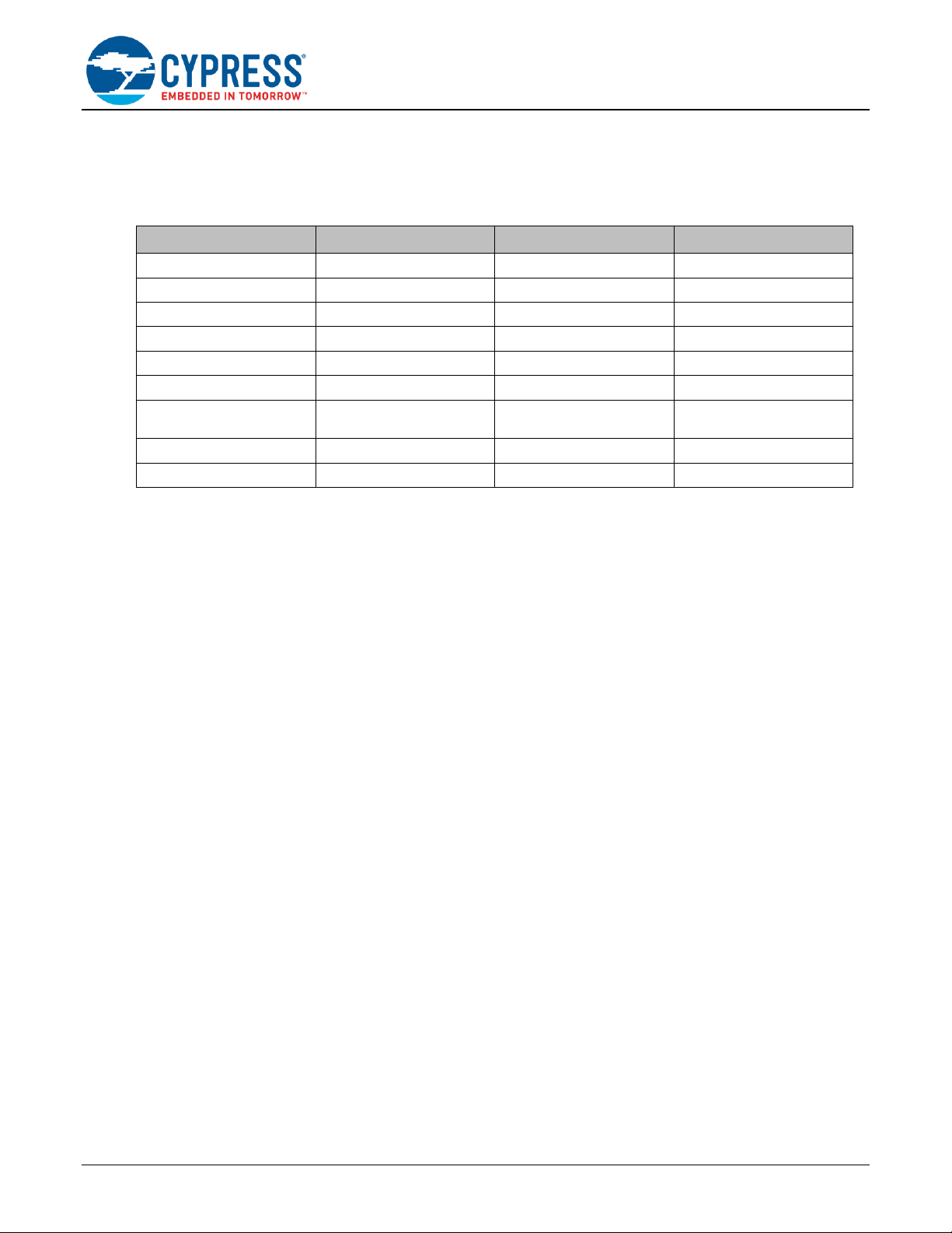
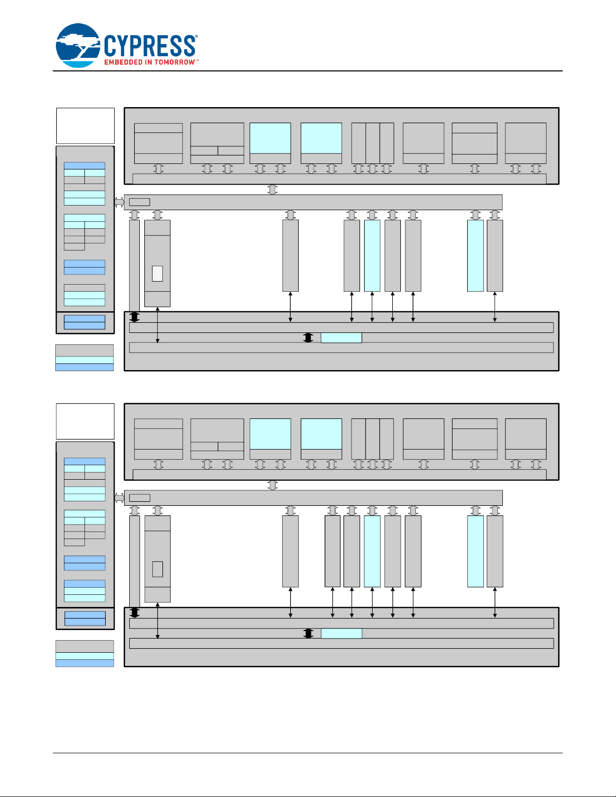
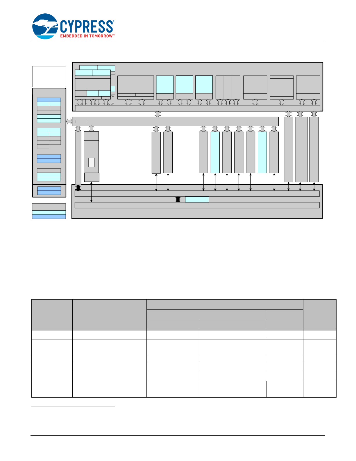
2.2 Product Overview
Traveo II Family is a family of 32-bit MCUs based on the high-performance Arm® Cortex®-M series of CPUs, as
Figure 1 shows, intended for automotive body-control applications.
The Cortex-M4 processor is the main CPU designed for a short interrupt response time, high code density, and high
32-bit throughput while maintaining a strict cost and power consumption budget. A secondary Cortex-M0+ based CPU
can implement security, safety, and protection features. Note that the CYT4BF series uses two Cortex-M7 processors
for primary processing.
Figure 1 through Figure 3 show the major architecture components of the CYT2B7 series, CYT2B9 series, and CYT4BF
series. There are four major subsystems: CPU subsystem, system resources, peripheral blocks, and I/O subsystem.
Page 4
Comparison of Traveo and Traveo II
www.cypress.com Document Number: 002-18629 Rev. *C 3
Figure 1. Block Diagram (CYT2B7 Series)
I/O Subsystem
Peripheral Interconnect (MMIO, PPU)
IOSS GPIO
PCLK
7x SCB
I
2
C, SPI, UART
Up to 146x GPIO std, Up to 6x GPIO Enh
CPU Subsystem
High Speed I/O Matrix, Smart I/O, Boundary Scan
1x SCB
I
2
C, SPI, UART
CYT2B7
MXS40-HT
ASIL-B
Digital DFT
Test
Analog DFT
System Resources
Power
Reset
Sleep Control
PWRSYS-HT
REF
POR
Reset Control
TestMode Entry
XRES
LVD
BOD
DeepSleep
Hibernate
Active/Sleep
LowPowerActive/Sleep
Power Modes
OVP
LDO
Clock
Clock Control
IMO
WDT
CSV
1xPLL
ECO
2xILO
FLL
79x TCPWM
Timer, CTR, QD, PWM
5x Smart IO
6x CANFD
CAN-FD Interface
EFUSE
1,024-bit
8x LIN
LIN/UART
Prog.
Analog
SAR
ADC
(12-bit)
x3
SARMUX
64-ch
System Interconnect (Multi-Layer AHB, IPC, MPU/SMPU)
Crypto
AES, SHA, CRC,
TRNG, RSA,
ECC
Initiator/MMIO
SWJ/MTB/CTI
MUL, NVIC, MPU
Arm
Cortex M0+
100 MHz
SWJ/ETM/ITM/CTI
Arm Cortex M4
160 MHz
FPU, NVIC, MPU
eCT Flash
Up to 1088 KB Code flash
+ Up to 96 KB Work flash
Flash Controller
8KB $ 8KB $
SRAM0
Up to 64KB
SRAM Controller
ROM
32KB
ROM Controller
SRAM1
Up to 64KB
SRAM Controller
M-DMA0
4-Channel
P-DMA1
33-Channel
P-DMA0
89-Channel
EVTGEN
Event Generator
WCO
RTC
Figure 2. Block Diagram (CYT2B9 Series)
I/O Subsystem
Peripheral Interconnect (MMIO, PPU)
IOSS GPIO
PCLK
7x SCB
I
2
C, SPI, UART
Up to 148x GPIO std, Up to 4x GPIO Enh
CPU Subsystem
High Speed I/O Matrix, Smart I/O, Boundary Scan
1x SCB
I
2
C, SPI, UART
CYT2B9
MXS40-HT
ASIL-B
Digital DFT
Test
Analog DFT
System Resources
Power
Reset
Sleep Control
PWRSYS-HT
REF
POR
Reset Control
TestMode Entry
XRES
LVD
BOD
DeepSleep
Hibernate
Active/Sleep
LowPowerActive/Sleep
Power Modes
OVP
LDO
Clock
Clock Control
IMO
WDT
CSV
1xPLL
ECO
2xILO
FLL
83x TCPWM
Timer, CTR, QD, PWM
5x Smart IO
8x CANFD
CAN-FD Interface
EFUSE
1,024-bit
12x LIN
LIN/UART
Prog.
Analog
SAR
ADC
(12-bit)
x3
SARMUX
64-ch
WCO
System Interconnect (Multi-Layer AHB, IPC, MPU/SMPU)
Crypto
AES, SHA, CRC,
TRNG, RSA,
ECC
Initiator/MMIO
SWJ/MTB/CTI
MUL, NVIC, MPU
Arm
Cortex M0+
100 MHz
SWJ/ETM/ITM/CTI
Arm Cortex M4
160 MHz
FPU, NVIC, MPU
eCT Flash
2112 KB Code flash +
128 KB Work flash
Flash Controller
8KB $ 8KB $
SRAM0
128 KB
SRAM Controller
ROM
32KB
ROM Controller
SRAM1
128 KB
SRAM Controller
M-DMA0
4-Channel
P-DMA1
44-Channel
P-DMA0
92-Channel
EVTGEN
Event Generator
4x CXPI
CXPI Interface
RTC
Page 5
Comparison of Traveo and Traveo II
www.cypress.com Document Number: 002-18629 Rev. *C 4
Figure 3. Block Diagram (CYT4BF Series)
I/O Subsystem
Up to 196x GPIO_STD, 4x GPIO_ENH, 40xHSIO
High Speed I/O Matrix, Smart I/O, Boundary Scan
CYT4BF
MXS40-HT
ASIL-B
Digital DFT
Test
Analog DFT
System Resources
Power
Reset
Sleep Control
PWRSYS-HT
REF
POR
Reset Control
TestMode Entry
XRES
LVD
BOD
DeepSleep
Hibernate
Active/Sleep
LowPowerActive/Sleep
Power Modes
OVP
LDO
Clock
Clock Control
IMO
WDT
CSV
4xPLL
ECO
2xILO
FLL
5x Smart IO
WCO
RTC
Peripheral Interconnect (MMIO,PPU)
IOSS GPIO
PCLK
CPU Subsystem
System Interconnect (Multi Layer AXI/AHB, IPC, MPU/SMPU)
115x TCPWM
TIMER,CTR,QD, PWM
10x CANFD
CAN-FD Interface
EFUSE
1x FLEXRAY
FlexRay Interface
SWJ/ETM/ITM/CTI
NVIC, MPU, AXI
Cortex M7
350 MHz
FPU
(SP/DP)
D$
16KB
I$
16KB
AHBSAHBP
ITCM
16 KB
DTCM
16 KB
SWJ/ETM/ITM/CTI
NVIC, MPU, AXI
Cortex M7
350 MHz
FPU
(SP/DP)
D$
16 KB
I$
16 KB
AHBSAHBP
ITCM
16 KB
DTCM
16 KB
eCT FLASH
8384 KB Code flash
+ 256 KB Work flash
FLASH Controller
8 KB $
10x SCB
I2C,SPI,UART,LIN
1x SCB
I2C,SPI,UART,LIN
20x LIN
LIN/UART
CRYPTO
AES,SHA,CRC,
TRNG,RSA,ECC
Initiator/MMIO
SWJ/MTB/CTI
MUL, NVIC, MPU
Cortex M0+
100 MHz
SRAM0
512 KB
SRAM
Controller
ROM
64 KB
ROM Controller
M-DMA0
8 Channel
P-DMA1
65 Channel
P-DMA0
143 Channel
1x SMIF
Serial Memory Interface (Hyperbus, Single SPI,
Dual SPI, Quad SPI, Octal SPI)
2x ETH
10/100/1000 Ethernet + AVB
SDHC
SD/SDIO/eMMC
EVTGEN
Event Generator
3x AUDIOSS
I2S/TDM In/Out
SRAM1
256 KB
SRAM
Controller
SRAM2
256 KB
SRAM
Controller
Prog.
Analog
SAR
ADC
(12-bit)
x3
SARMUX
96 ch
2.3 On-chip System Features
2.3.1 CPU
Both Traveo and Traveo II family are based on 32-bit Arm Cortex processors.
Traveo family has a single Cortex-R5 processor, while Traveo II family is a dual-CPU with Cortex-M4 and Cortex-M0+
processors. In Traveo II, two CPUs are configured as the CPU subsystem; Cortex-M4 or Cortex-M7 processor is the
main CPU and Cortex-M0+ processor is the secondary CPU that can implement security, safety, and protection features.
Note that as the CPU core changes, MCU features change according to the core specification.
Table 3. Differences in CPU
Item
Traveo Family
Traveo II Family
Remarks
Main CPU
Secondary
CPU
CYT2B7/B9 Series
CYT4BF Series
CPU Core
Cortex-R5F
Cortex-M4
Cortex-M7 (x2)
Cortex-M0+
Operation
Frequency
Up to 132 MHz
Up to 160 MHz
Up to 350 MHz
Up to 100 MHz
Product
specifications
FPU
Single/Double precision
Single precision
Single/Double precision
None
MPU
16 regions
8 regions
16 regions
8 regions
1
Cache Memory
I-cache 16 KB / D-cache 16 KB
None
I-cache 16 KB / D-cache 16 KB
None
TCM Interface
Supported
Implemented TCRAM
Not supported
Supported (ITCM, DTCM)
Not supported
1
Traveo II family has SMPU as memory protection in addition to the CPU's internal MPU. Refer to 2.3.14 Protection.
Page 6
Comparison of Traveo and Traveo II
www.cypress.com Document Number: 002-18629 Rev. *C 5
Item
Traveo Family
Traveo II Family
Remarks
Main CPU
Secondary
CPU
CYT2B7/B9 Series
CYT4BF Series
Support for
Interrupt
Controller
Vector Interrupt Controller (VIC)
Nested Vector Interrupt Controller (NVIC)
2.3.2 Memory Design
Table 4 lists the Code Flash features. The main differences are in program size, Read-While-Write operation, and
redundancy.
Table 4. Differences in Code Flash
Code Flash
S6J3428/9/A Series
CYT2B7/B9, CYT4BF Series
ECC
SEC/DED
SEC/DED
Sector Size
32 KB, 8 KB
32 KB, 8 KB
Program Size
32 bits, 64 bits, 256 bits
64 bits, 256 bits, 4096 bits
Program and Erase
Cycles/Retention
1000/20 years
1000/20 years
Read-While-Write Operation
Not supported
Supported
Table 5 lists the Work Flash features. The main differences are in the sector size, program and erase cycles, Read-
While-Write operation, and redundancy. When compared to Traveo, Traveo II families support smaller sector size and
higher program and erase cycles.
Table 5. Differences in Work Flash
Work Flash
S6J3428/9/A Series
CYT2B7/B9, CYT4BF Series
ECC
SEC/DED
SEC/DED
Sector Size
4 KB
2 KB, 128 B
Program Size
32 bits
32 bits
Program and Erase
Cycles/Retention
1000/20 years
10000/10 years
100000/5 years
125000/20 years
250000/10 years
Read-While-Write
Operation
Not supported
Supported
Table 6 lists the SRAM features. The main difference is the data retention in low power mode. Traveo II family supports
data retention in DeepSleep mode.
Table 6. Differences in SRAM
SRAM
S6J3428/9/A Series
CYT2B7/B9, CYT4BF Series
ECC
SEC/DED
SEC/DED
Data Retention in Low
Power Mode
Not supported
(TCRAM and SRAM are not retained in
Shutdown mode. Backup RAM is retained in
Shutdown mode)
Supported
(SRAM is retained in DeepSleep mode)
Page 7
Comparison of Traveo and Traveo II
www.cypress.com Document Number: 002-18629 Rev. *C 6
2.3.3 Debug
Traveo and Traveo II families support JTAG and SWD Debug Interface. Table 7 shows the main differences in
debugging.
Table 7. Differences in Debugging
Item
S6J3428/9/A Series
CYT2B7/B9, CYT4BF Series
Debug interface
JTAG
SWD
JTAG
SWD
2.3.4 Mode Setting
Traveo II family does not support the serial programming mode; therefore, there is no mode pin in Traveo II family.
When the debugger is connected to JTAG, Traveo II family transitions to Debug mode and enables programming to
flash.
Table 8. Differences in Mode Setting
Item
S6J3428/9/A Series
CYT2B7/B9, CYT4BF Series
Normal Mode
Setting by mode pin
• User Mode
Debugger is not connected (SWD or JTAG)
• Boot mode/user mode/trusted mode
• Life cycle stage (Secure)
Board mode
Setting by mode pin
• Serial programming mode
• Parallel programming mode
Debugger is connected (SWD or JTAG)
• Debug mode
• Life cycle stage (Normal_Provisioned
/Secure/Secure_With_Debug/RMA/
Corrupted)
2.3.5 Power Supply and Monitoring
The power supply of Traveo II family is the same as that of Traveo family, but signal names of power supply are
different. Also, the type of power monitoring mode has been enhanced in Traveo II family.
2.3.5.1 Power Supply
Table 9 lists the power supply and differences in functionality.
Table 9. Power Supply
Power Supply
S6J3428/9/A Series
CYT2B7/B9, CYT4BF Series
External
Digital
VCC
2.7 to 5.5 V
V
DDD
2.7 to 5.5 V
I/O
V
DDIO_1/2
2.7 to 5.5 V
V
DDIO_3/4
2.7 to 3.6 V (only for CYT4BF series)
Analog
AVCC0/1
2.7 to 5.5 V
V
DDA
2.7 to 5.5 V
Internal
C
1.2 V
V
CCD
1.1 V
V
CCD
of CYT4BF can be also external
power supply (typical 1.15 V when V
CCD
is
external power supply)
Page 8
Comparison of Traveo and Traveo II
www.cypress.com Document Number: 002-18629 Rev. *C 7
2.3.5.2 Monitoring
Table 10 lists the differences in voltage between Traveo and Traveo II families.
Table 10. Voltage Monitoring
Monitoring
S6J3428/9/A Series
CYT2B7/B9, CYT4BF Series
Voltage Monitoring
• Power-on reset (POR)
• LVD
• POR
• LVD
• Brownout detection (BOD)
• Overvoltage detection (OVD)
• Overcurrent detection (OCD)
2.3.6 Reset Factor
Note that all resets in Traveo II family are asynchronous resets. This difference is because the reset factor is optimized
according to the Traveo II system. If you need the RAM retention Reset, see the Architecture Technical Reference
Manual (TRM). Table 11 lists the main differences in Reset Factor.
Table 11. Differences in Reset Factors
Reset Sources
S6J3428/9/A Series
CY2B7/B9, CYT4BF Series
Remarks
POR
Yes
Yes
BOD Reset
• External LVD Reset
• Internal LVD Reset
• RAM retention LVD Reset
• External voltage BOD Reset
2
• Internal voltage BOD Reset
3
• Analog input voltage BOD Reset
2,4
OVD Reset
No
• External voltage OVD Reset
2
• Internal voltage OVD Reset
3
• Analog input voltage OVD Reset
2,4
OCD Reset
No
Internal voltage OCD Reset3
External Reset
RSTX pin
XRES_L pin
Clock Stop Wait
Timeout Reset
Yes
No, does not support synchronous reset
Illegal Mode Detection
Reset
Yes
No, does not have MD pin
Profile Error Reset
Yes
No, does not support Profile setting
Watchdog Timer (WDT)
Reset
• Hardware WDT Reset
• Software WDT Reset
• WDT Reset
• Multi-Counter WDT Reset
See 2.3.8
Watchdog Timer
Internal System
(Software) Reset
• Software Reset
• Software trigger hard Reset
• Software Reset
Fault Detection Reset
No
Yes: via Fault report
2
Programmable Trip point (2 points)
3
Fixed Trip point
4
Reset or Fault report can be selected
Page 9
Comparison of Traveo and Traveo II
www.cypress.com Document Number: 002-18629 Rev. *C 8
Reset Sources
S6J3428/9/A Series
CY2B7/B9, CYT4BF Series
Remarks
Clock Supervision
(CSV) Reset
• Main Clock CSV Reset
• Sub Clock CSV Reset
• PLL Clock CSV Reset
• SSCG Clock CSV Reset
• Fast CR CSV Reset
• Slow CR CSV Reset
• CLK_REF CSV Reset
• ILO0 CSV Reset
• CLK_HF CSV Reset
• CLK_LF CSV Reset
Wakeup Reset
Yes (Power Domain Reset)
Yes (Hibernate Wake up Reset)
Debugger Reset
• TRSTX
• Software Reset
• NTRST
• Software Reset
2.3.7 Clock System
Compared to Traveo family clock system, Traveo II family (only CYT4B Series) has Spread Spectrum Clock Generator
functions. In Traveo II family, frequency-locked loop (FLL) featuring fast startup and low power is implemented.
Table 12 lists the main differences in clock system.
See the datasheet for the AC characteristics of each clock.
Table 12. Differences in Clock System
Clock System
Traveo Family
(S6J3428/9/A Series)
Traveo II Family
(CYT2B Series)
Traveo II Family
(CYT4B Series)
Internal Clock Source
Fast CR: 4 MHz
(Using source clock after
reset)
Slow CR: 100 kHz
IMO: 8 MHz
(Using source clock after reset)
ILO0/1: 32 kHz
External Clock Source
Main clock: 3.6 to 16 MHz
Sub clock: 32.768 kHz
ECO: 3.988 to 33.33 MHz
WCO: 32.768 kHz
EXT_CLK5 : 0.25 to 100 MHz
High-Speed
Clock Generation
PLL
PLL x1
Input: 3.6 to 17.6 MHz
Output: 200 to 320 MHz
SSCG PLL x1
Input: 3.6 to 32MHz
Output:200 up to 320 MHz
PLL x1
Input: 3.988 to 33.34 MHz
Output: 11 to 160 MHz
SSCG not supported
PLL without SSCG x2
Input: 3.988 to 33.34 MHz
Output: 11 to 200 MHz
PLL with SSCG x2
Input: 3.988 to 33.34 MHz
Output: 25 to 400 MHz
FLL
Not implemented
FLL x1
Input: 0.25 to 80 MHz
Output: 24 to 100 MHz
FLL x1
Input: 0.25 to 80 MHz
Output: 24 to 100 MHz
Clock Gear
Supported
Not implemented
Clock Supervision
Main clock
Sub clock
PLL clock
SSCG clock
Slow CR
Fast CR
CLK_REF (IMO or ECO or EXT_CLK)
CLK_HF (PLL and FLL)
ILO0
CLK_LF (ILO1 or WCO)
5
It can be sourced from a designated I/O pin.
Page 10
Comparison of Traveo and Traveo II
www.cypress.com Document Number: 002-18629 Rev. *C 9
2.3.8 Watchdog Timer
Table 13 lists the watchdog timer (hardware) features. The main differences are counter clock, maximum timeout, and
the behavior during low-power mode and debugging.
Table 13. Differences in Watchdog Timer (Hardware)
Watchdog Timer
(Hardware)
S6J3428/9/A Series
CY2B7/B9, CYT4BF Series
Trigger
Reset
Reset
Counter Clock
• Fast internal clock: 4 MHz
• Slow internal clock: 100 kHz
• Internal low speed oscillator: 32 kHz
Counter
32 bits
32 bits
Maximum Timeout
12 hours
38.33 hours
Window Function
Supported
Supported
Warning Interrupt
Supported
Supported
Timeout Expiration Action
Reset or nonmaskable interrupt (NMI)
Reset
Behavior During Low-Power
Mode
Stop
Register can select stop or run
Behavior During Debugging
Stop at debugging state
Register can select stop or run
Table 14 lists the multi-counter watchdog timer (software) features. The main differences are counter clock, counter,
maximum timeout, and the behavior during debugging.
Table 14. Differences in Multi-Counter Watchdog Timer (Software)
Multi-counter Watchdog
Timer (Software)
S6J3428/9/A Series
CY2B7/B9, CYT4BF Series
Trigger
User program
User program
Counter Clock
• Fast internal clock: 4 MHz
• Slow internal clock: 100 kHz
• Main clock: 4 to 16 MHz
• Sub clock: 32 kHz
• Internal low-speed oscillator: 32 kHz
• Watch crystal oscillator: 32 kHz
Counter
32 bits
2 * 16-bit, 32 bits only for interrupt
Maximum Timeout
36.4 hours
2.11 seconds
Window Function
Supported
Supported
Warning Interrupt
Supported
Supported
Timeout Expiration Action
Reset or NMI
Reset or Fault
Behavior During Low-Power
Mode
Register can select stop or run.
Register can select stop or run.
Behavior During Debugging
Stop at debugging state
Register can select stop or run.
Page 11
Comparison of Traveo and Traveo II
www.cypress.com Document Number: 002-18629 Rev. *C 10
2.3.9 Low-Power Mode
Table 15 lists the low-power modes. Traveo II family supports almost all low-power modes with DeepSleep mode.
Table 15. Differences of Low-Power Modes
Low Power Mode
S6J3428/9/A Series
CY2B7/B9, CYT4BF Series
Sleep
• CPU: Halt
• Peripheral: Active
• SRAM retention
Supported: Sleep
• TCRAM/SRAM/Backup RAM retention
Supported: Sleep
• SRAM retention
Timer
• CPU: Halt
• Peripheral: Halt except RTC,
GPIO
• SRAM retention
Supported: Timer
• TCRAM/SRAM/Backup RAM retention
Supported: DeepSleep
• Peripheral: OFF except RTC, Event
generator, GPIO
• SRAM retention
Stop
• CPU: Halt
• Peripheral: Halt except
GPIO
• SRAM retention
Supported: Stop
• TCRAM/SRAM/Backup RAM retention
Supported: DeepSleep
• Peripheral: OFF except RTC, Event
generator, GPIO
• SRAM retention
Partial wakeup (Shutdown)
• CPU: OFF
• Peripheral: OFF except
RTC, ADC, GPIO
• Partial RAM retention
Supported: Partial wakeup
• ADC is triggered by RTC
• Backup RAM retention
Supported: DeepSleep
• Peripheral: OFF except RTC, Event
generator, GPIO
• ADC and LIN are triggered by Event
generator
• SRAM retention (Full/Partial)
Timer (Shutdown)
• CPU: OFF
• Peripheral: OFF except
RTC, GPIO
• Partial RAM retention
Supported: Timer (Shutdown)
• Backup RAM retention
Supported: DeepSleep
• Peripheral: OFF except RTC, Event
generator, GPIO
• SRAM retention (Full/Partial)
Stop (Shutdown)
• CPU: OFF
• Peripheral: OFF except
GPIO
• Partial RAM retention
Supported: Stop (Shutdown)
• Backup RAM retention
Supported: DeepSleep
• SRAM retention (Full/Partial)
Page 12
Comparison of Traveo and Traveo II
www.cypress.com Document Number: 002-18629 Rev. *C 11
2.3.10 Interrupt Structure
The interrupt structure of Traveo and Traveo II families differ based on the CPU. Traveo family (Cortex-R5) interrupt
controller used vector interrupt controller (VIC), while Traveo II family (Cortex-M4//M7/M0+) uses nested vector interrupt
controller (NVIC). Table 16 lists the main differences in interrupt structure.
Traveo family controls system interrupts such as enable/disable, levels, and level masks with an external interrupt
controller. Each CPU of Traveo II family has eight interrupt inputs, and controls interrupts within the CPU, thereby
performing high-speed interrupt processing.
Traveo II family uses up to 1023 system interrupts assigned to eight groups. All interrupts within a group has the same
priority. Four of the 1023 system interrupts can be assigned as NMI.
Traveo II family implements wakeup interrupt controller (WIC), which enables interrupt detection for CPU wakeup in
DeepSleep power mode.
Table 16. Differences of Interrupt Structure
Item
S6J3428/9/A Series
CY2B7/B9, CYT4BF Series
Remarks
CPU core
Cortex-R5F
Cortex-M4/M7
Cortex-M0+
Supported Interrupt
Controller in CPU
VIC
NVIC
Number of IRQ
inputs of CPU
1 8 8
Number of NMI
Inputs of CPU
1 1 1
Priority Level
Interrupt: 32 levels
NMI: 16 levels
Interrupt: 8 levels
NMI: None
Interrupt: 4 levels
NMI: None
Number of System
Interrupts
Up to 512
Up to 1023
6
Vector Address
Assigned for each system
interrupt
Assigned for each IRQ input.
Multiple system interrupts share a CPU
interrupt handler as provided by the VTOR
table.
WIC
Not Supported
Supported
6
System Interrupts are interrupts generated from peripheral functions and external inputs. For the list of system interrupts supported
by the device variants, see the following documents:
- Traveo Family: Hardware Manual by the device variants.
- Traveo II Family: Architecture Technical Reference Manual by the device variants
Page 13
Comparison of Traveo and Traveo II
www.cypress.com Document Number: 002-18629 Rev. *C 12
2.3.11 Data Transfer
For data transfer, Traveo II family has two types of DMA with different purposes: Peripheral DMA (P-DMA) and Memory
DMA (M-DMA). Table 17 lists the main differences in data transfer.
P-DMA focuses on achieving low latency for a large number of channels. P-DMA has a single data transfer engine that
is shared by all channels.
M-DMA focuses on achieving high memory bandwidth for a small number of channels. M-DMA has a dedicated data
transfer engine for each channel.
The DMA transfer specification of Traveo family is set by the register. In Traveo II family, transfer is specified by the
descriptor in SRAM. P/M-DMA of Traveo II family can perform transfer chaining with descriptor setting.
Table 17. Differences of Data Transfer
Item
S6J3428/9/A Series
CY2B7/B9, CYT4BF Series
Remarks
Function Name
DMAC
P-DMA
M-DMA
Data Transfer Specifics
Register
Descriptor in memory
Data Size
8-/16-/32-/64-bit
8-/16-/32-bit
Transfer Mode
• Single
• Block
• Burst
• Single
• 1D/2D
• CRC transfer
• Descriptor chaining
• Single
• 1D/2D
• Memory copy
• Scatter
• Descriptor chaining
Activation Trigger
• Hardware
• Software
• Hardware
• Software
• Transfer completion
trigger output
• Software
• Transfer completion
trigger output
Channel Arbitration
Schemes
• Fixed
• Dynamic
• Round robin
• Fixed four levels
• Round-robin in the same priority group
Interrupt Generation
• Transfer
Completion
• Error occurrence
• Transfer completion
• Error occurrence
Protection Schemes
Dedicated MPU
• Access range
• User/Privilege
• Read/Write
SMPU and PPU
• Access range
• User/Privileged
• Read/Write
• Secure/Non-secure
• Protection Contexts
See Protection.
Page 14
Comparison of Traveo and Traveo II
www.cypress.com Document Number: 002-18629 Rev. *C 13
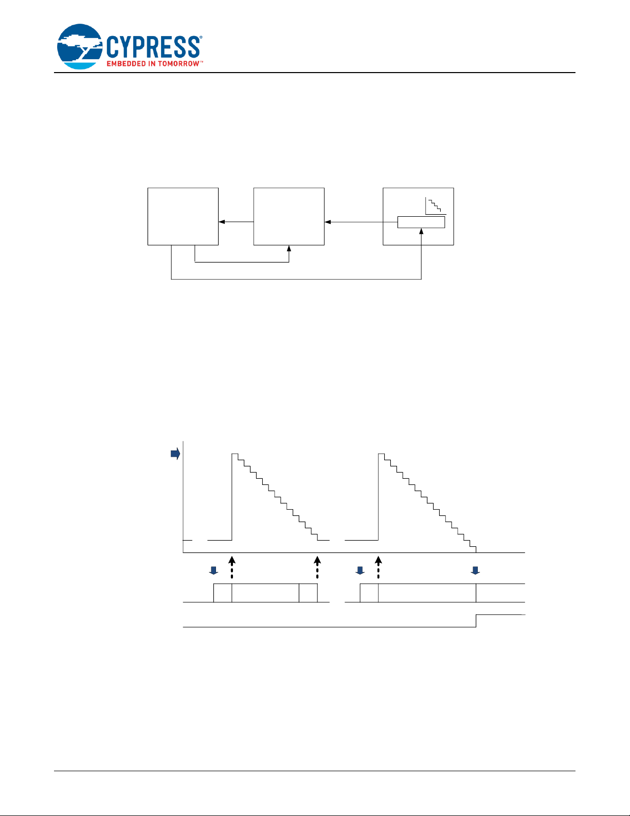
2.3.12 TPU
Traveo family has a dedicated timer for timing protection (TPU). However, Traveo II family does not have a dedicated
timer. Traveo II family uses a TCPWM timer for timing protection.
The TCPWM timer is a general-purpose timer that can generate interrupts for overflow, underflow, and compare
matches. This interrupt can be implemented as NMI, which can provide the TPU function. Figure 4 shows the
configuration of the TPU and Figure 5 shows an example of the operation.
Figure 4. Timing Protection Implementation Example
CPU tcpwmInterrupt
Controller
NMI
Timer
(5) Underflow
(1),(3),(4)
(5)
(2)
(3) Start Down Count
1. Configure the TCPWM initial values (for example, using DownCount mode), and set the upper limit of the
measurement time as the initial time.
2. Set the TCPWM interrupt to NMI.
3. Software starts the timer at the start point of the measurement process.
4. Software stops the timer at the end point of the measurement process.
5. If the counter under-flowed before the software stops the timer, the Underflow interrupt of the TCPWM is notified
as an NMI to the CPU via the interrupt controller.
Note: The interrupt controller can notify the system interrupt as NMI, including the TCPWM interrupt.
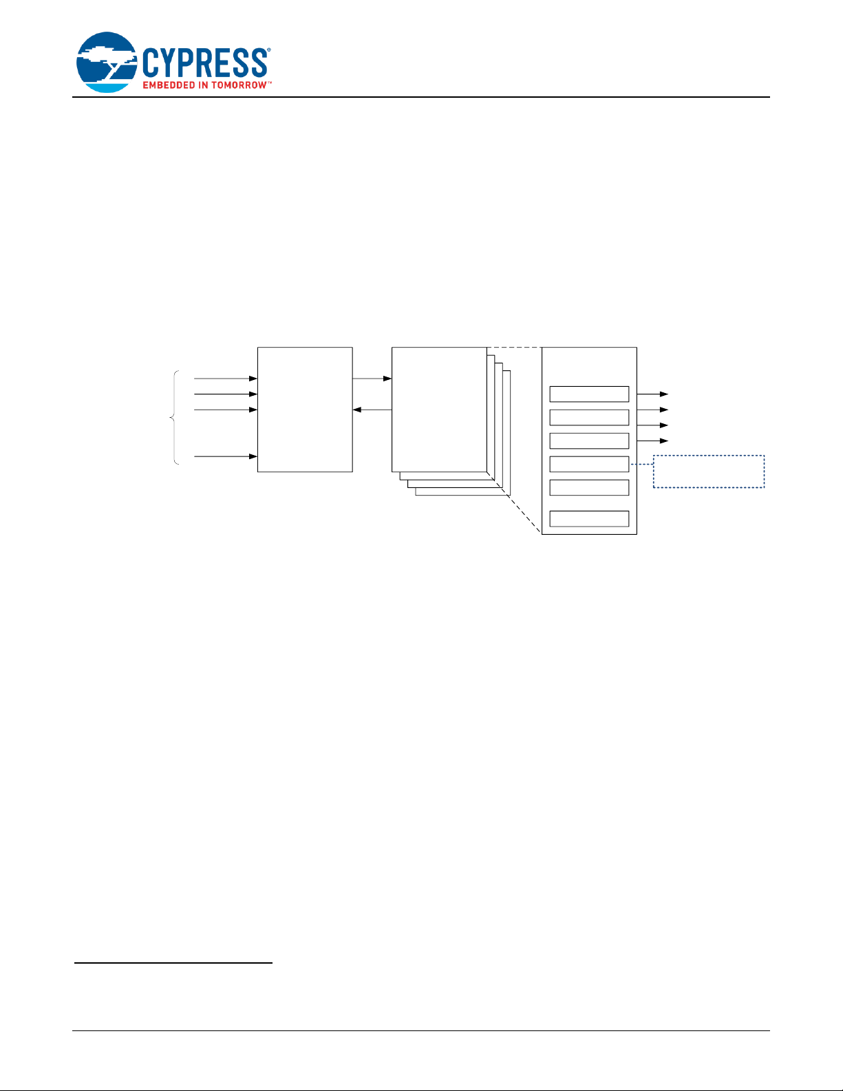
Figure 5. Timing Protection Example (Monitoring of the Interrupt Service Routine Operation Time)
Timer
Initial value
Interrupt
Timer
Start
Timer
Stop
Interrupt operation
Interrupt
Timer
Start
Interrupt operation
||||
||
||
Under flow
Interrupt
Service Routine
NMI
Interrupt Timeout
Page 15
Comparison of Traveo and Traveo II
www.cypress.com Document Number: 002-18629 Rev. *C 14
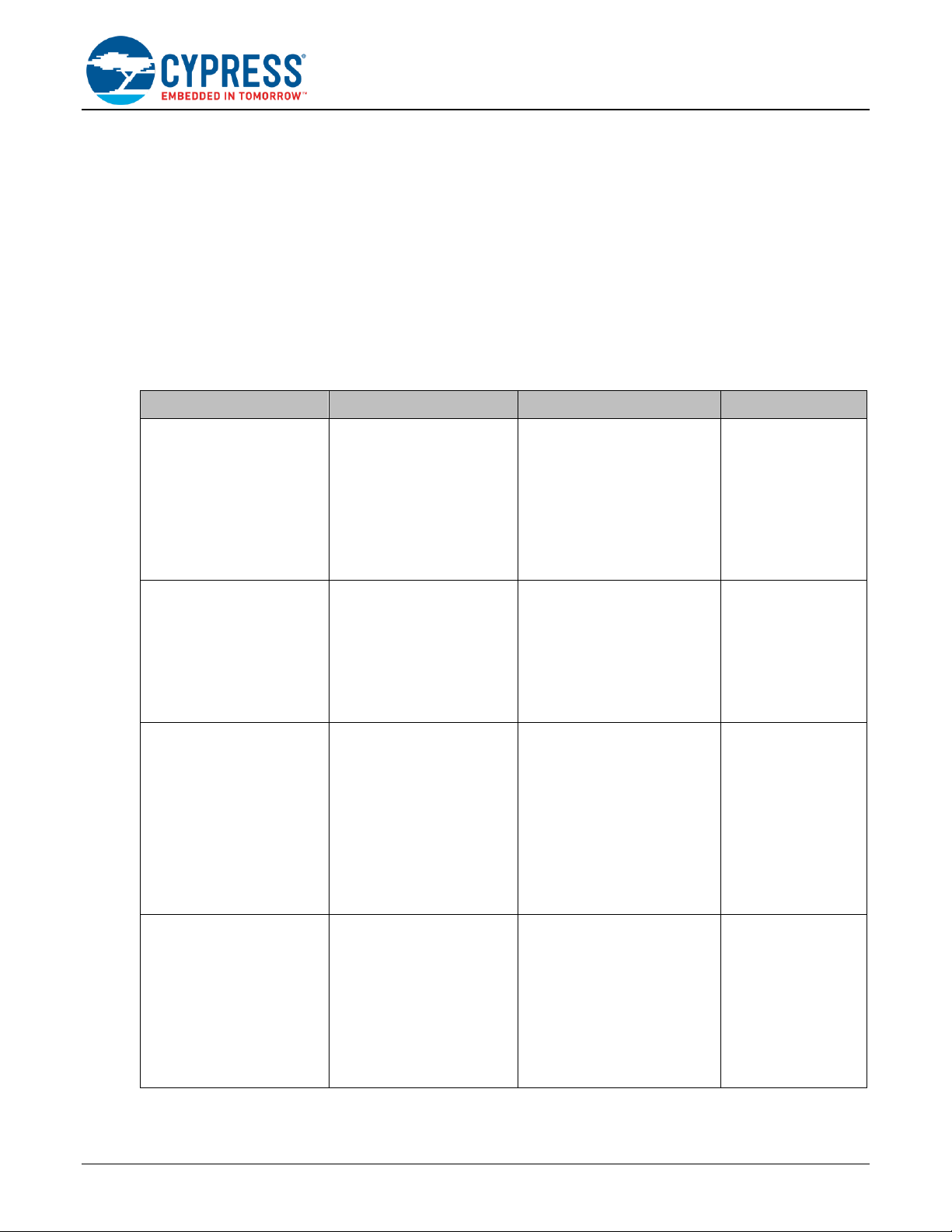
2.3.13 Fault Report
Fault report is a new feature of Traveo II family. Figure 6 shows a block diagram of the Fault structure.
The centralization of faults by Fault report structures for a system-wide consistent handling of faults simplifies software
development.
Fault report captures up to 967 failures such as MPU/SMPU/PPU protection violations, SRAM controller ECC errors,
peripheral-specific errors, and so on. When Fault report captures a fault, it generates a notification signal such as fault
interrupt, trigger output, external pin output, and fault reset request. Each of these output signals can be enabled or
disabled.
The fault interrupt can be mapped to the CPU NMI as a system interrupt. In addition, Fault report provides the fault
source and additional fault-specific information.
For more details, see the Traveo II Architecture Technical Reference Manual (TRM).
Figure 6. Fault Structure
Fault report
Pending Faults
Fault report
Fault report
Fault Report
Structure
Fault Report
Structure
Data0-7
Fault Control
Status
MASK0-2
INT Control
PENDING0-2
・
・
Fault Source
(Up to 96)
Fault Reset
Interrupt
Trigger
Out Signal
Fault source and
additional information
7
For the list of system interrupts supported by the device variants, see the Technical Reference Manual.
Page 16
Comparison of Traveo and Traveo II
www.cypress.com Document Number: 002-18629 Rev. *C 15
2.3.14 Protection
The Protection function of Traveo family consists of the CPU's Memory Protection Unit (MPU), DMA's MPU, and
Peripheral Protection Unit (PPU). Traveo II family consists of MPU, Shared Memory Protection Unit (SMPU), and PPU.
Table 18 lists the main differences in Protection Units.
In Traveo II family, memory protection is provided by MPU and SMPU. MPU is implemented as part of the CPU and
bus infrastructure. P-DMA, M-DMA, and encrypted components do not have MPU. Instead, they inherit the access
control attributes of programmed bus transfer.
SMPU is shared by all masters; PPU is a protection unit for peripheral registers.
Traveo II family supports a new protection attribute (Secure/Non-secure), and protection contexts. Protection contexts
can change the access restriction without changing the setting of the protection unit.
For more details, see the Technical Reference Manual.
Table 18. Differences in Protection Configuration and Access Attribute
Item
S6J3428/9/A Series
CY2B7/B9, CYT4BF Series
Remarks
MPU implemented in the CPU
Cortex-R5: 16 Regions
Access Attribute:
• Access Range
• Privileged/Unprivileged
• Read/Write
• Execute (Code or Data)
Cortex-M4/M0+: 8 Regions
Cortex-M7: 16 Regions
Access Attribute:
• Access Range
• Privileged/Unprivileged
• Read/Write
• Execute (Code or Data)
MPU implemented in the bus
infrastructure
Not supported
16 Regions
Access Attribute:
• Access Range
• Privileged/Unprivileged
• Read/Write
• Execute (Code or Data)
For external master
such as debugger
SMPU
Not supported
16 Regions
Access Attribute:
• Access Range
• Privileged/Unprivileged
• Read/Write
• Execute (Code or Data)
• Secure/Non-secure
• Protection Contexts
PPU
Access Attribute:
• USER/Privilege
• Read/Write
Access Attribute:
• Access Range
• Privileged/Unprivileged
• Read/Write
• Execute (Code or Data)
• Secure/Non-secure
• Protection Contexts
Page 17
Comparison of Traveo and Traveo II
www.cypress.com Document Number: 002-18629 Rev. *C 16
Item
S6J3428/9/A Series
CY2B7/B9, CYT4BF Series
Remarks
MPU16-AHB
Access Attribute:
• Access range
• USER/Privilege
• Read/Write
Not supported.
DMA access protection is
provided by SMPU and PPU.
2.3.15 Boot Process
The boot process of both Traveo and Traveo II families is executed after reset and before the application program
starts. The boot process is executed by the Cortex-R5 processor in Traveo family, and is executed by the secure master
(Cortex-M0+ processor) in Traveo II family.
The boot process in Traveo family mainly executes based on the operation mode and the security setting that the
debugger connection authenticates, secure boot processing, and hardware watchdog timer according to the flash
marker.
In Traveo II family, the boot process consists of ROM boot and flash boot. The ROM boot process determines the
Protection State and validates the flash boot process. The flash boot process configures the protection unit such as
SMPU and PPU, and verify the application program code in the flash memory. In addition, activates the boot loader.
For more details, see the Technical Reference Manual.
2.3.16 Security
Table 19 lists the security features. Traveo II family supports lifecycle stages, device protection states, and Hardware
Security Module (HSM).
Table 19. Differences of Security
Security
S6J3428/9/A Series
CY2B7/B9, CYT4BF Series
Lifecycle stages
Device protection states
Not supported
Supported
• Lifecycle stages
• Protection states
Flash protection
Supported
Supported
Debugger security
Supported
Supported
Hardware-based
encryption
Supported
Secure Hardware Extension (SHE)
Supported
Enhanced Secure Hardware Extension (eSHE)
and HSM support are enabled by third-party
firmware.
Page 18
Comparison of Traveo and Traveo II
www.cypress.com Document Number: 002-18629 Rev. *C 17
2.4 Peripherals
2.4.1 Timer
The Timer function of Traveo family consists of a Base timer, Reload timer, Free-run timer, Input Capture, Output
compare, and Quadrature Position/Revolution Counter (QPRC).
Traveo II family implements TCPWM with integrated multiple timer functions. The TCPWM has seven operation modes.
All TCPWM channels can be operated by selecting one of the seven modes. Table 20 lists the corresponding modes
of each function.
Table 20. TCPWM Channel Modes
Function Name
S6J3428/9/A Series
CY2B7/B9, CYT4BF Series
Timer Mode
Base timer: Reload Timer mode
Free-run Timer
Reload Timer
TCPWM: Timer mode
Capture Mode
Input Capture
Base timer: PWC Timer mode
TCPWM: Capture mode
Quadrature
Decoder
QPRC
TCPWM: QUAD mode
PWM Mode
Output compare
Base timer: PWM Timer mode
Base timer: PPG Timer mode
TCPWM: PWM mode
PWM with Dead
Time
Not supported
TCPWM: PWM_DT mode
Pseudo-Random
PWM
Not supported
TCPWM: PWM_PR mode
Shift Register
Not supported
TCPWM: SR mode
Page 19

Comparison of Traveo and Traveo II
www.cypress.com Document Number: 002-18629 Rev. *C 18
2.4.1.1 Base Timer: Reload Timer Mode
The Base Trimer Reload mode in Traveo family is a timer that counts down from a set value. When the timer value
reaches ‘0’, the timer stops or starts counting down from the set value again. Also, an event can be generated if the
timer value is ‘0’. In Traveo II family, the same operation is possible using TCPWM Timer mode. Table 21 lists the main
differences in Base Timer Reload Timer modes between Traveo and Traveo II families.
Table 21. Differences in Base Timer: Reload Timer Mode
Counter
S6J3428/9/A Series
CY2B7/B9, CYT4BF Series
Timer Function
Base Timer: Reload Timer mode
TCPWM: Timer mode
Counter Width
16 bits or 32 bits (uses two 16-bit timer)
16 bits or 32 bits
Count Mode
Down
Up, Down, Up-down1/2
Operation Clock
Internal clock: 12 types:
/1, /2, /4, /8, /16, /32, /64, /128, /256, /512, /1024 or
/2048
Internal clock: 8 types:
/1, /2, /4, /8, /16, /32, /64 or /128
External clock:
Rising-edge, falling-edge, or both-edge
Not supported8
Operation mode
One shot mode:
Stop event is underflow
One shot mode:
Stop event depends on count mode. (underflow,
overflow or both)
Reload mode
Reload mode
Gate function
Supported
Supported
Activation
Software
Software: via Trigger Multiplexer
External trigger
External trigger
External Timer Match Starting
Not supported
Event Generation
Underflow
TC event:
TC event depends on count mode. (underflow,
overflow or both)
Timer Activation trigger
Not Supported
Not supported
Compare match event
Debug Mode
Supported
Supported
8
The external clock cannot be used as the timer's count clock. However, when the count event is used in the rising edge (supported
falling and both edge) detection mode, the timer will count with count event detection. In this case, the count event can be used as
the external clock.
Page 20

Comparison of Traveo and Traveo II
www.cypress.com Document Number: 002-18629 Rev. *C 19
2.4.1.2 32-bit Free-run Timer
The Free-run timer in Traveo family counts up or up-down within a set value. In Traveo II family, the same operation is
possible using TCPWM Timer mode. However, in Traveo II family there is no interrupt mask count function. Table 22
lists the main differences in Free-run Timer.
Table 22. Differences in 32-bit Free-run Timer
Counter
S6J3428/9/A Series
CY2B7/B9, CYT4BF Series
Timer function
32-bit Free-run Timer
TCPWM: Timer mode
Counter width
32 bits
16 bits or 32 bits
Count mode
Up, Up-down
Up, Down, Up-down1/2
Operation clock
Internal clock: 9 types:
/1, /2, /4, /8, /16, /32, /64, /128 or /256
Internal clock: 8 types:
/1, /2, /4, /8, /16, /32, /64 or /128
External clock:
Both-edge
Not supported9
Operation mode
Not Supported
One shot mode:
Stop event depends on the count mode (underflow,
overflow, or both)
Reload mode
Reload mode
Buffer function
Supported
Supported
Activation
Software
Software: via Trigger Multiplexer
Not supported
External trigger
Event Generation
Compare clear
Zero Detection
TC event:
TC event depends on count mode (underflow,
overflow, or both)
Not supported
Compare match event
Interrupt mask count Function
Not Supported
Debug Mode
Supported
Supported
9
The external clock cannot be used as the timer's count clock. However, when the count event is used in the rising edge (supported
falling and both edge) detection mode, the timer will count with count event detection. In this case, the count event can be used as
the external clock.
Page 21

Comparison of Traveo and Traveo II
www.cypress.com Document Number: 002-18629 Rev. *C 20
2.4.1.3 32-bit Reload Timer
The 32-bit Reload mode in Traveo family is a timer that counts down from a set value. In Traveo II family, the same
operation is possible using TCPWM Timer mode. Table 23 lists the main differences in 32-bit Reload Timer.
Table 23. Differences of 32-bit Reload Timer
Counter
S6J3428/9/A Series
CY2B7/B9, CYT4BF Series
Timer Function
32-bit Reload Timer
TCPWM: Timer mode
Counter Width
32 bits
16 bits or 32 bits
Count Mode
Down
Up, Down, Up-down1/2
Operation Clock
Internal clock: 6 types:
/1, /2, /4, /8, /16 or /32
Internal clock: 8 types:
/1, /2, /4, /8, /16, /32, /64 or /128
External clock:
Rising-edge, falling-edge, or both edges
Not supported10
Operation Mode
One shot mode:
Stop event is underflow
One shot mode:
Stop event depends on count mode (underflow,
overflow, or both)
Reload mode
Reload mode
Gate Function
Supported
Supported
Activation
Software
Software: via Trigger Multiplexer
External trigger
External trigger
Event Generation
Underflow
TC event:
TC event depends on count mode (underflow,
overflow, or both)
Not supported
Compare match event
Simultaneous Soft
Start
Supported
Supported: via Trigger Multiplexer
Debug Mode
Supported
Supported
10
The external clock cannot be used as the timer's count clock. However, when the count event is used in the rising edge (supported
falling and both edge) detection mode, the timer will count with count event detection. In this case, the count event can be used as
the external clock.
Page 22

Comparison of Traveo and Traveo II
www.cypress.com Document Number: 002-18629 Rev. *C 21
2.4.1.4 32-bit Input Capture
The 32-bit input capture function in Traveo family measures the input pulse width and external clock cycle based on
the value of the 32-bit free-run timer. In Traveo II family, the same operation is possible using the TCPWM capture
mode.
In Traveo family, the Input capture function is a linkage function with the free-run timer, but Traveo II family has an
independent timer for each TCPWM channel. Therefore, Traveo II family does not need a different timer for the Input
Capture function. Table 24 lists the main differences in 32-bit Input Capture.
Table 24. Differences in 32-bit Input Capture
Counter
S6J3428/9/A Series
CY2B7/B9, CYT4BF Series
Timer Function
32-bit Input Capture
TCPWM: Capture mode
Counter Width
32 bits
16 bits or 32 bits
Count Mode
Follow Free-run Timer
Up, Down, Up-down1/2
Operation Mode
Follow Free-run Timer
One shot mode:
Stop event depends on count mode. (underflow,
overflow or both)
Reload mode
Clock Pre-scaling
Follow Free-run Timer
Internal clock: 8 types:
/1, /2, /4, /8, /16, /32, /64 or /128
Capture Event
Rising-edge, falling-edge, or both-edge
Supported: via Trigger Multiplexer
Buffer Function
Not supported
Double buffer
Counter value is copied to the capture register and
capture register is copied to the capture buffer
register when a Capture event is detected.
Event Generation
Capture event detection
Counter value is captured.
2.4.1.5 Base Timer: PWC Timer Mode
Base Timer: PWC Timer mode in Traveo family measures the time and cycle between any input pulse events by using
a counter.
Traveo II family does not have the same operation mode. However, the TCPWM capture mode can measure via
software the time between two events using two buffers. Figure 7 shows an example of the operation.
Figure 7. Example for Pulse Width Count Measurements
0 1 2 3 4 5 6 7 8 9 10
Counter Value
Capture Event
1 8
1 5
5
Capture register
Capture buff register
Pulse width
(By software)
4 3
Page 23

Comparison of Traveo and Traveo II
www.cypress.com Document Number: 002-18629 Rev. *C 22
2.4.1.6 QPRC
The Quadrature decoder is used to measure the position of position encoder. Both Traveo and Traveo II families
implement Quadrature Decoder.
Both support x 1, x 2, x 4 count modes. However, Revolution counter operation mode is not supported in Traveo II
family. Table 25 lists the main differences in QPRC.
Table 25. Differences in QPRC
Counter
S6J3428/9/A Series
CY2B7/B9, CYT4BF Series
Timer function
QPRC
TCPWM: QUAD mode
Counter width
Two 16 bits (Position counter, Revolution counter)
16 bits or 32 bits
Position counter
Operation mode
Up/Down count mode
Up/Down Rotary mode
Not Supported
x 1 encoding
Phase difference count mode x2 mode
Count edge: phi_B
x 2 encoding
Count edge: phi_A
Phase difference count mode x4 mode
x 4 encoding
Count mode with direction
Not Supported
Revolution counter
Operation mode
RC_mode1
Not supported
RC_mode2
RC_mode3
Event Generation
Count inversion
Not Supported
Zero index
tc event with Reload/Index event
Overflow
Supported
QUAD_RANGE1_CMP, QUAD_RANGE1_CAPT
Under flow
Supported
QUAD_RANGE1_CMP, QUAD_RANGE1_CAPT
PC and RC match
Not Supported
PC match
Supported:
QUAD_RANGE0_CMP
QUAD_RANGE1_CMP
PC match and RC match
Not Supported
Out range
Not Supported
Capture
Not Supported
Supported: QUAD_RANGE1_CAPT
Debug Mode
Not Supported
Supported
Page 24

Comparison of Traveo and Traveo II
www.cypress.com Document Number: 002-18629 Rev. *C 23
2.4.1.7 32-bit Output Compare
The 32-bit output compare in Traveo family generates the PWM waveform with 32-bit Free-run timer. In addition, events
can be generated at compare match. In Traveo II family, the same operation is possible using TCPWM PWM mode.
Table 26 lists the main differences in 32-bit Reload Timer.
Table 26. Differences in 32-bit Output Compare
Counter
S6J3428/9/A Series
CY2B7/B9, CYT4BF Series
Timer function
32-bit Output compare
TCPWM: PWM mode
Counter width
32 bits
16 bits or 32 bits
Count mode
Up, Up-down
Up, Down, Up-down1/2
Operation clock
9 types Internal Clock
• /1, /2, /4, /8, /16, /32, /64, /128 or /256
Internal clock: 8 types
• /1, /2, /4, /8, /16, /32, /64 or /128
External clock
- Both-edge
Not supported11
Buffer function
Supported
Supported
Compare registers
per channel
Two
Two
Output pins per
channel
Two
• OUT0 for compare register 0
• OUT1 for compare register 1
Two
• LINE_OUT is an output
• LINE_COMPL_OUT is a complementary output
One shot mode
Not Supported
One shot mode:
• Stop event depends on count mode. (underflow,
overflow or both)
Signal output
Invert mode
Supported
Set/Reset mode
Supported
Activation
Software
Software: via Trigger Multiplexer
Not supported
External trigger
Compare match
Supported
Not Supported
TC event:
• TC event depends on count mode. (underflow,
overflow or both)
Kill modes
Not supported
Supported
Debug Mode
Supported
Supported
11
External clock cannot be used as the timer's count clock. But, when the count event is used in rising edge (supported falling and
both edge) detection mode, timer will count by count event detection. In this case, count event can be used as external clock.
Page 25

Comparison of Traveo and Traveo II
www.cypress.com Document Number: 002-18629 Rev. *C 24
2.4.1.8 Base Timer: PWM Timer Mode
Base Trimer PWM mode in Traveo family can output waveforms of the set cycle either singly or continuously upon the
detection of a trigger. In this mode, cycle and duty are set to generate PWM waveform.
In Traveo II family, the same operation is possible using TCPWM PWM mode. Table 27 lists the main differences in
Base Timer PWM Mode.
Table 27. Differences in Base Timer: PWM Timer Mode
Counter
S6J3428/9/A Series
CY2B7/B9, CYT4BF Series
Timer Function
Base Timer: PWM mode
TCPWM: PWM mode
Counter Width
16 bits
16 bits or 32 bits
Count Mode
Down
Up, Down, Up-down1/2
Operation Clock
Internal clock: 12 types
/1, /2, /4, /8, /16, /32, /64, /128, /256, /512, /1024 or
/2048
Internal clock: 8 types
/1, /2, /4, /8, /16, /32, /64 or /128
External clock:
Rising-edge, falling-edge, or both-edge
Not supported12
Operation Mode
One shot mode:
Stop event is underflow
One shot mode:
Stop event depends on count mode. (underflow,
overflow or both)
Continuous mode
Reload mode
Start Delay
Supported
Not Supported13
Buffer Function
Supported
Supported
Activation
Software
Software: via Trigger Multiplexer
External trigger
External trigger
External Timer Match Starting
Not supported
Signal Output
1: Inverted output when cycle and duty match
2: Inverted output when compare match
LINE_OUT and LINE_COMPL_OUT
Right-aligned PWM
Left-aligned, Right-aligned,
Center-aligned, Asymmetric PWM
Output polarity control
Supported
Trigger Output
A/D convertor activation
Supported
Event Generation
Underflow
TC event:
TC event depends on count mode. (underflow,
overflow or both)
Duty match
Supported: compare match
Start Trigger Detection
Not Supported
Debug Mode
Supported
Supported
12
The external clock cannot be used as the timer's count clock. However, when the count event is used in the rising edge (supported
falling and both edge) detection mode, the timer will count with count event detection. In this case, the count event can be used as
the external clock.
13
Counters can be pre-loaded with values reflecting the desired phase shift and then started synchronously. Note that during the initial
(start delay) period, some counters can already generate the PWM output, depending on the duty cycle.
Page 26

Comparison of Traveo and Traveo II
www.cypress.com Document Number: 002-18629 Rev. *C 25
2.4.1.9 Base Timer: PPG Timer Mode
The Base Trimer PPG mode in Traveo family can output single or continuous waveforms with the configured cycle
either when a trigger is detected. In this mode, ‘L’ width and ‘H’ width are set to generate the PPG waveform.
In Traveo II family, the same operation is possible using TCPWM mode. Table 28 lists the main differences in Base
Timer: PPG Timer Mode.
Table 28. Differences in Base Timer: PPG Timer Mode
Counter
S6J3428/9/A Series
CY2B7/B9, CYT4BF Series
Timer Function
Base Timer: PPG mode
TCPWM: PWM mode
Counter Width
16 bits
16 bits or 32 bits
Count Mode
Down
Up, Down, Up-down1/2
Operation Clock
Internal clock: 12 types
/1, /2, /4, /8, /16, /32, /64, /128, /256, /512, /1024 or
/2048
Internal clock: 8 types:
/1, /2, /4, /8, /16, /32, /64 or /128
External clock:
Rising-edge, falling-edge, or both-edge
Not supported14
Operation mode
One shot mode:
Stop event is underflow
One shot mode:
Stop event depends on count mode. (underflow,
overflow or both)
Continuous mode
Reload mode
Activation
Software
Software: via Trigger Multiplexer
External trigger
External trigger
Signal Output
1
Inverted output when cycle and duty match
2
• Inverted output when compare match
• LINE_OUT and LINE_COMPL_OUT
Output polarity control
Supported
Event Generation
Underflow
TC event:
TC event depends on count mode. (underflow,
overflow or both)
Start Trigger Detection
Not Supported
Debug Mode
Supported
Supported
14
The external clock cannot be used as the timer's count clock. However, when the count event is used in the rising edge (supported
falling and both edge) detection mode, the timer will count with count event detection. In this case, the count event can be used as
the external clock.
Page 27

Comparison of Traveo and Traveo II
www.cypress.com Document Number: 002-18629 Rev. *C 26
2.4.1.10 TCPWM: PWM_DT Mode
This mode adds Dead time to the PMW output waveform. This function is not supported in Traveo family. Figure 8
shows an example of the operation. The PWM_DT functionality is the same as the PWM functionality except for the
following differences:
▪
PWM_DT supports dead time insertion; PWM does not support dead time insertion.
▪
PWM_DT does not support clock pre-scaling; PWM supports clock pre-scaling.
For more details, see the Technical Reference Manual.
Figure 8. Dead Time Timing
Line_out
Line_compl_out
Dead time = 0
Line_out
Line_compl_out
Dead time = 1
Line_out
Line_compl_out
Dead time = 2
1
2
2.4.1.11 TCPWM: PWM_PR Mode
This functionality changes the counter value using the linear feedback shift register (LFSR). This results in a pseudo
random number sequence; the generated signal has frequency/noise characteristics different from a regular PWM
signal. This function is not supported in Traveo family. Figure 9 shows an example of the operation.
For more details, see the Technical Reference Manual.
Figure 9. PWM_PR Output
COUNTER
0
reload
0xffff
LINE_OUT
Page 28

Comparison of Traveo and Traveo II
www.cypress.com Document Number: 002-18629 Rev. *C 27
2.4.1.12 TCPWM: SR Mode
This functionality shifts the counter value to the right. This implements a signal delay function from the trigger input to
the line output, which can be used for functions such as detecting frequency shift keying (FSK) signals. This function
is not supported in Traveo family. Figure 10 shows an example of the operation. For more details, see the TRM.
Figure 10. SR Mode Operation
reload
Serial-in
Line_out
COUNTER
(Shift register)
0x8000 0x4000 0xA000 0x5000 0x2800 0x1400 0x0A00 0x0500 0x0280 0x0140 0x00A0 0x0050 0x0028 0x0014 0x000A 0x0005 0x0002 0x0001 0x00000x0000
PERIOD_BUFF
(Counter Tap)
15-cycle
0x0002 (15 cycle delay)
PWM line output is generated from an XOR combination of enabled counter taps (bit position) defined by
PERIOD_BUFF.
2.4.2 Serial Communication Block
The serial communication function realized by MFS on Traveo family is realized by SCB in Traveo II family. In Traveo
II family, the LIN function is realized by a dedicated module.
Table 29. Differences in Serial Communication Block
Item
S6J3428/9/A Series
CY2B7/B9, CYT4BF Series
Function name
Multi-Function Serial (MFS)
Serial communication Block (SCB)
LIN
Supported function
• UART
• CSIO (SPI Supported)
• I2C
• LIN (v2.1)
• UART
• SPI
• I2C
LIN (v 2.2A)
2.4.2.1 UART
Traveo II family SCB (UART) data transmission and reception are always executed in FIFO mode. In Traveo II family,
eight out of nine SCB blocks support full UART, and one SCB does not support UART mode. Table 30 lists the main
differences.
Table 30. Differences in UART
Item
S6J3428/9/A Series
CY2B7/B9, CYT4BF Series
Data
Transmission and reception FIFOs (64 bytes
each) (when FIFOs are used)
Transmission/reception FIFO (32/256/512 bytes
each) (FIFO mode only)
Serial Input
Oversampling is performed 3 times by the bus
clock. The reception value is determined by
majority decision.
• Use clk_scb
▪ Use input clock (clk_scb) as "oversampling
multiple" of interface clock
Transfer Format
Asynchronous
Asynchronous
Baud Rate
Dedicated baud rate generator (15-bit reload
counter configuration)
CTRL.OVS register supported
• Baud rate= clk_scb / (OVS + 1) *OVS=7-15
The external clock input can be adjusted by the
reload counter.
Not supported
Page 29

Comparison of Traveo and Traveo II
www.cypress.com Document Number: 002-18629 Rev. *C 28
Item
S6J3428/9/A Series
CY2B7/B9, CYT4BF Series
Data Length
5 to 9 bits (for normal mode), or 7 to 8 bits (for
multi-processor mode)
4 to 16 bits (Standard/Multi-processor mode)
Signaling Method
NRZ
NRZ
Inverted NRZ
Not supported
Start Bit Detection
Synchronized to falling edges of the start bit (for
NRZ method)
Synchronized with the start bit falling edge (NRZ
system)
Synchronized to rising edges of the start bit (for
inverted NRZ method)
Not supported
Reception Error
Detection
Framing error
Framing error
Overrun error
Not supported
Parity error
(Normal mode only)
Parity support
(Odd parity and even parity)
Hardware Flow
Control
Transmission/reception auto control by CTS and
RTS
Transmission/reception auto control by CTS and
RTS
Interrupt Request
Reception interrupt
Reception interrupt
(Frame error, Parity error)
Reception FIFO interrupt
Reception FIFO interrupt
(RX FIFO is full, RX FIFO is not empty, RX FIFO
overflow, RX FIFO underflow)
Transmission interrupt
Transmission interrupt (TX done)
Transmission FIFO interrupt
Transmission FIFO interrupt
(TX FIFO is not full, TX FIFO is empty
TX FIFO overflow, TX FIFO underflow)
DMA transfer is supported for both transmission
and reception
Not supported
Status interrupt
Not supported
Master/Slave-Type
Communication
Function (MultiProcessor Mode)
1 (master) -to-n (slave) communication is
supported.
(Both master and slave systems are supported.)
1 (Master)-to-n (slave)
communication is supported
(Both master and slave systems are supported)
FIFO option
Transmission and reception FIFOs are provided
Transmission and reception FIFOs are supported
Transmission FIFO and reception FIFO can be
selected
Not supported
Transmission data can be retransmitted
Not supported
The timing of the reception FIFO interrupt can be
changed by software
The timing of the reception FIFO interrupt can be
changed by software
Independent FIFO reset is supported
Independent FIFO reset is supported
Page 30

Comparison of Traveo and Traveo II
www.cypress.com Document Number: 002-18629 Rev. *C 29
2.4.2.2 I2C
Traveo II family SCB (I2C) data transmission and reception are always executed in FIFO mode. In Traveo II family,
eight out of nine SCB blocks support full I2C and one SCB supports only I2C slave mode. Table 31 lists the main
differences.
Table 31. Differences in I2C
Item
S6J3428/9/A Series
CY2B7/B9, CYT4BF Series
Data Buffer
Full duplex-double buffer (FIFO is unused).
Single memory buffer.
(EZ I2C /Command-RESP).
Transmission/reception FIFO (16 bytes each)
(when FIFO is used).
Transmission/reception FIFO (32/256/512 bytes
each) (FIFO mode only).
Serial Input
For serial clock and data input, noise from 2 to up
to 38 bus clocks is filtered out.
Filtering glitches up to 50 ns.
Transfer Mode
Synchronization
Synchronization
Baud Rate
Dedicated baud rate generator provided
(comprising 15-bit reload counter).
• Slow mode (50 kbps)
• Standard mode (100 kbps)
• Fast mode (400 kbps)
• Fast mode plus (1000 kbps)
Data Length
8 bits
8 bits
Signaling Method
NRZ
NRZ
Interrupt Request
Reception interrupt
Reception interrupt.
(I2C STOP detection at the end of each transfer,
I2C STOP detection at the end of a read transfer).
Transmission interrupt.
Transmission interrupt.
(I2C STOP detection at the end of each transfer,
I2C STOP detection at the end of a write
transfer).
Status interrupt.
(INT interrupt, stop condition interrupt, repeated
start detection interrupt, serial timer interrupt).
Status interrupt.
(I2C master lost arbitration, I2C master received
NACK, I2C master received ACK, I2C bus error,
I2C slave lost arbitration, I2C slave received
NACK, I2C slave received ACK, I2C slave
received STOP, I2C slave received START, I2C
slave address matched, I2C bus error)
Transmission FIFO interrupt (A transmission
FIFO overrun error occurs when the transmission
FIFO is not higher than the interrupt trigger level
or when the transmission FIFO is empty).
Transmission FIFO interrupt (TX FIFO is not full,
TX FIFO is empty, TX FIFO overflow, TX FIFO
underflow).
Reception FIFO interrupt (reception FIFO under
run)
Reception FIFO interrupt (RX FIFO is full, RX
FIFO is not empty, RX FIFO overflow, RX FIFO
underflow).
A DMA transfer support function is provided for
both transmission and reception.
Not supported
Not supported
Wake up request on address match
Page 31

Comparison of Traveo and Traveo II
www.cypress.com Document Number: 002-18629 Rev. *C 30
Item
S6J3428/9/A Series
CY2B7/B9, CYT4BF Series
FIFO
• Transmission and reception FIFOs are
provided (64 bytes for the transmission FIFO
and 64 bytes for the reception FIFO).
• The transmission FIFO and reception FIFO can
be selected.
• Transmission data can be retransmitted.
• The reception FIFO interrupt timing can be
changed by software.
• Independent FIFO reset is supported.
• Transmission/reception FIFO (32/256/512
bytes).
• The transmission FIFO and reception FIFO can
be selected.
• Transmission data can be retransmitted.
• The reception FIFO interrupt timing can be
changed by software.
Clock Stretching
Supported
Supported
I2C Mode
Supported
• Master
• Slave
• Multi-master
Supported
• Master
• Slave
• Multi-master
2.4.2.3 SPI
Traveo II family SCB (SPI) data transmission and reception are always executed in FIFO mode. In Traveo II family,
eight out of nine SCB blocks support full SPI, and one SCB supports only SPI slave mode. Table 32 lists the main
differences.
Table 32. Differences in SPI
Item
S6J3428/9/A Series
CY2B7/B9, CYT4BF Series
Data Buffer
Transmission and reception FIFOs (64 bytes
each) (when FIFO is used)
Transmission/reception FIFO (32/256/512 bytes
each) (FIFO mode only)
Transfer Format
Clock synchronization (no start/stop bits)
Clock synchronization (no start/stop bits)
Master/slave functions
Master/slave functions
Supports SPI (supports both master and slave)
Supports SPI (supports both master and slave)
Baud Rate
A dedicated baud rate generator is provided
(configured from a 15-bit reload counter, during
master operation).
Maximum 8 Mbps
• CTRL.OVS register supported
• Baud rate= clk_scb / (OVS + 1) *OVS=3-15
Maximum 12 Mbps
External clock input is enabled (during slave
operation)
Supports externally clocked slave operation
Data Length
5 to 16, 20, 24, and 32 bits
Data frame size programmable from 4 bits to 32
bits
Page 32

Comparison of Traveo and Traveo II
www.cypress.com Document Number: 002-18629 Rev. *C 31
Item
S6J3428/9/A Series
CY2B7/B9, CYT4BF Series
Interrupt Request
Reception interrupt
• Reception completion
• Overrun error
• Reception block transfer error
Not supported
Reception FIFO interrupt
• Reception FIFO under run
Reception FIFO interrupt
• RX FIFO is full
• RX FIFO is not empty
• RX FIFO overflow
• RX FIFO underflow
Transmission interrupt
• Transmission data empty
• Transmission bus idle
• Chip error interrupt
• Transmission block transfer error
Transmission interrupt
• SPI master transfer done
• SPI Bus Error.
• SPI slave deselected after any EZSPI transfer
occurred
• SPI slave deselected after a write EZSPI
transfer occurred
Transmission FIFO interrupt
• When the transmission FIFO is not higher than
the interrupt trigger level
• When the transmission FIFO is empty,
transmission FIFO overrun
Transmission FIFO interrupt
• TX FIFO is not full
• TX FIFO is empty
• TX FIFO overflow
• TX FIFO underflow
DMA Transfer support function is provided for
both transmission and reception
Not supported
Status interrupt
• Serial timer interrupt
Status interrupt
• Wake up request on slave select
• SPI STOP detection at the end of each transfer
• SPI STOP detection at the end of a write
transfer
• SPI STOP detection at the end of a read
transfer
Serial Chip Select
• Four-channel control (independent control,
rounding control)
• The setup/hold/deselect times can be made
variable
• The active level can be selected for each
channel
• Supports up to four slave select lines
Synchronous Mode
Master or slave function
Master or slave function
Page 33

Comparison of Traveo and Traveo II
www.cypress.com Document Number: 002-18629 Rev. *C 32
Item
S6J3428/9/A Series
CY2B7/B9, CYT4BF Series
FIFO Option
• Incorporates transmission and reception FIFOs
(64 bytes for transmission FIFO, 64 bytes for
reception FIFO)
• The transmission and reception FIFOs can be
selected
• Transmission data can be retransmitted
• The timing of the reception FIFO interrupt can
be changed by software
• Independent FIFO reset is supported
• Transmission/reception FIFO equipped
(transmission FIFO: 32/256/512 bytes,
reception FIFO: 32/256/512 bytes)
• Reception FIFO interrupt timing can be
modified by software
• FIFO reset is supported independently
2.4.2.4 LIN
The Traveo II family LIN block supports autonomous forwarding of LIN frames. Table 33 lists the main differences.
Table 33. Differences in LIN
Item
S6J3428/9/A Series
CY2B7/B9, CYT4BF Series
Serial Input
Over sampling is performed by the bus clock 3
times. The reception value is determined by
the rule of majority.
3 times oversample (noise filter) at sample point.
Transfer Mode
Asynchronous
Asynchronous
Baud Rate
• Dedicated baud rate generator is provided
(consisting of a 15-bit reload counter).
• The external clock can be adjusted by the
reload counter.
• Auto baud rate adjustment with Sync Field
reception.
• Set for each channel
▪ baud rate adjustment by receiving Sync Field
by application
Data Length
8 bits
8 bits
Signaling Method
NRZ
NRZ
Start Bit Detection
Synchronized with falling edges of the start bit
Synchronized with falling edges of the start bit
Error Detection
• Framing error
• Overrun error
• Transmitter bit error
• Receive synchronization error
• Receiver PID error
• Receiver frame error
• Response checksum error
• Timeout detection
• Transmitter bit error
• Receive synchronization error
• Receiver frame error
• Receiver PID parity error
• Response checksum error
• Receiver noise detection
Page 34

Comparison of Traveo and Traveo II
www.cypress.com Document Number: 002-18629 Rev. *C 33
Item
S6J3428/9/A Series
CY2B7/B9, CYT4BF Series
Interrupt Request
Reception interrupt
• Reception completion
• Reception block transfer error
Reception interrupt
• RX break wakeup done
• RX header sync done
• RX header done
• RX response done
Reception FIFO interrupt
• Reception FIFO underrun
Not supported
Transmission interrupt
• TX data empty
• TX bus idle
• TX block transfer error
Transmission interrupt
• TX header done
• TX response done
• TX wakeup done
Status interrupts
• LIN Break Field detection
• Serial timer interrupt
Status interrupts
• Receiver noise detection
• Time out detection
Interrupt request to ICU
• LIN Sync Field detection: LSYN
Not supported
Transmission FIFO interrupt
• When the transmission FIFO is within the
interrupt threshold
• When the transmission FIFO is empty
• Transmission FIFO overrun
Not supported
DMA transfer is supported for both transmission
and reception.
Not supported
LIN Bus Option
• Support for LIN Protocol Revision 2.1
• Master device operation (auto and manual
mode)
• Slave device operation (only manual mode)
• Auto header transmission
• Auto response transmission
• Auto response reception
• Detection of the start/stop edge of the LIN sync
field connected to an input capture
• LIN break field generation (manual mode)
• LIN break delimiter generation (manual mode)
• LIN break field detection (manual mode)
• LIN protocol support in hardware according to
ISO 17987 standard
• Master device operation (auto mode)
• Slave device operation (auto mode)
• Auto header transmission
• Auto response transmission
• Auto response reception
Wakeup Pulse
• Reception not supported
• Transmission not supported
• Reception supported
• Transmission supported
LIN Transceiver
Control
• Not supported
• Supported
UART protocol
• Not supported
• Supported
Page 35

Comparison of Traveo and Traveo II
www.cypress.com Document Number: 002-18629 Rev. *C 34
2.4.3 CAN FD
Table 34 lists the CAN FD features. Traveo II family shares the message RAM and Timestamp function for global
channel control. Traveo II family supports the receive FIFO top pointer for DMA transfer.
Table 34. Differences in CAN FD
CAN FD
S6J3428/9/A Series
CY2B7/B9, CYT4BF Series
Classical CAN
Supported
Supported
CAN FD
Supported
Supported
TTCAN
Not supported
Supported
Message Buffer15
• 64 (Extended ID]) + 128 (Standard ID]) Rx
filters
• 2 * 64 MSG Rx FIFO + 64 MSG dedicated Rx
buffers
• 32 MSG dedicated Tx buffers
• 32 event Tx FIFO
• 64 (Extended ID]) + 128 (Standard ID]) Rx
filters
• 2 * 64 MSG Rx FIFO + 64 MSG dedicated Rx
buffers
• 32 MSG dedicated Tx buffers
• 32 event Tx FIFO
Message Handler
1 1 Message RAM Access
Direct access
Direct access
Message RAM
Dedicated type
Shared type
Message RAM with
ECC
Supported
Supported
Timestamp Function
Supported
Supported
• Shared Timestamp counter
Receive FIFO Top
Pointer
Not supported
Supported
2.4.4 I/O Interface
Table 35 lists the I/O interface features. The main differences are the input threshold selection, output drive strength
selection, noise filter, and Smart IO.
Table 35. Differences in I/O Interface
I/O Interface
S6J3428/9/A Series
CY2B7/B9, CYT4BF Series
Input Threshold
Selection
• CMOS (0307)
• Automotive (0508)
• TTL
Supported except TTL
Supported
15
For Traveo and Traveo II the listed numbers indicate the maximum addressable message buffers; utilization depends on available
MRAM size.
Page 36

Comparison of Traveo and Traveo II
www.cypress.com Document Number: 002-18629 Rev. *C 35
I/O Interface
S6J3428/9/A Series
CY2B7/B9, CYT4BF Series
Output Drive Strength
Selection
Supported
• 1 mA
• 2 mA
• 3 mA only for I2C
• 5 mA
Supported
• 0.5 mA
• 1 mA
• 2 mA
• 5 mA
• 6 mA only for GPIO (IOL)
• 10 mA only for HSIO_STD (Only for CYT4BF)
Pull-up / Pull-down
Supported
• 50 kΩ (typ)
Supported
• 50 kΩ (typ)
High-Z State
Supported
Supported
Port Status Hold During
Low-Power Mode
Supported
Supported
Noise Filter
Supported per port pin
• Max 100 ns
Supported per port group
• Max 50 ns
Smart IO
Not supported
Supported
2.4.5 ADC
Table 36 lists the ADC features. The main differences are the result data format, averaging, and pre-conditioning.
Table 36 Differences in ADC
ADC
S6J3428/9/A Series
CY2B7/B9, CYT4BF Series
12-bit Resolution
Supported
Supported
Logical Channel
Supported
Supported
Software Trigger
Supported
Supported
Hardware Trigger
Supported
Supported
Idle Trigger
(Continuous)
Supported
• Idle trigger
Supported
• Continuous
Result Data per Each
Channel
Supported
• Single buffer
Supported
• Double buffer
Result Data Format
• Unsigned (fixed)
• Right alignment (fixed)
• 8-bit/10-bit/12-bit
• Sign/unsigned
• Left/right alignment
• Max 16-bit (Sign/zero extension),
Programmable right shift
Programmable Sample
Time per Each
Channel
Supported
• Select one from four 16-bit register
• ≥ 7 cycles
Supported
• 12-bit registers per each channel
• ≥ 11 cycles
Comparison Time
≥ 16 cycles (16-bit register)
15 cycles (Fixed)
Page 37

Comparison of Traveo and Traveo II
www.cypress.com Document Number: 002-18629 Rev. *C 36
ADC
S6J3428/9/A Series
CY2B7/B9, CYT4BF Series
Range Detection
• Supported
• Select one from eight thresholds (above/below)
register per each channel
• Inside/Outside
• Supported
• Thresholds (above/below) registers per each
channel
• Inside/Outside/Above/Below
Pulse Detection
Supported
• 8-bit Positive counter
• 5-bit Negative counter
Supported
• 8-bit Positive counter
• 5-bit Negative counter
Averaging
Not supported
Supported
Group Scan
Supported
Supported
Preemption Types
when Group
Interrupted
Supported
• Resume
• Restart
• Stop
Supported
• ABORT_RESUME
• ABORT_RESTART
• ABORT_CANCEL
• FINISH_RESUME
Priority
Supported
• 16 priorities per channel
Supported
• 8 priorities per group
Interrupt
Supported
• Per channel/group conversion done
• Per channel range detect
• Per channel pulse detect
• Group interrupted
Supported
• Per channel range detect
• Per channel pulse detect
• Per channel/group overflow
• Group/channel done
• Group cancelled
DMA Request
Supported
Supported
Calibration
Supported
• Analog calibration
Supported
• Analog calibration
• Alternate calibration
• Coherent calibration update
Pre-conditioning
Not supported
Supported
• Off
• VREFL
• VREFH
• Diagnostic reference voltage
Diagnostic Reference
Voltage
Supported
• AVRL
• AVRH
Supported
• 10 voltage levels from VREFL to VREFH
Power Down Mode
Supported
Supported
Debug Mode
Supported
Supported
Software Abort
Supported
• Forced stop
Supported
• IP disable
Page 38

Comparison of Traveo and Traveo II
www.cypress.com Document Number: 002-18629 Rev. *C 37
2.4.6 RTC
Table 37 lists the RTC features. The main differences are the source clock, interrupts, and the counters of half-
second/month/year.
Table 37. Differences of RTC
RTC
S6J3428/9/A Series
CY2B7/B9, CYT4BF Series
Source Clock
Main clock oscillator (4 MHz)
Sub clock oscillator (32 kHz)
Internal low speed oscillator (100 kHz)
Watch Crystal oscillator (32 kHz)
Internal low speed oscillator (32 kHz)
Half-second Counter
Supported
Not supported
• Event Generator can count less than a second
Second Counter
Supported
Supported
Minute Counter
Supported
Supported
Hour Counter
Supported
Supported
Day Counter
Supported
Supported
Month Counter
Not supported
Supported
Year Counter
Not supported
Supported
Automatic Leap Year
Correction
Not supported
Supported
Interrupt
Each counter (Day/Hour/Minute/Second/Halfsecond)
Two independent alarms (Month + Day + Hour +
Minute + Second)
Calibration
Supported
• Automatic calibration by main clock
Supported
• Calibration by waveform output and software
2.4.7 CRC
In Traveo family, CRC was implemented in a dedicated CRYPT and DMA module.
Table 38. Differences in CRC
Item
S6J3428/9/A Series
CY2B7/B9, CYT4BF Series
Method
Supported CRC module
• CCITT CRC16 (polynomial = "0x1021")
• IEEE-802.3 CRC32 (polynomial =
"0x04C11DB7")
Supported CRYPT module and DMA module
• CCITT CRC16 (polynomial = "0x1021")
• IEEE-802.3 CRC32 (polynomial =
"0x04C11DB7")
2.4.8 CXPI
Traveo II family has a CXPI module only in CYT2B9 series MCUs.
CXPI supports the following:
▪
CXPI protocol support in hardware according to ISO/WD 20794-4
▪
Master node
Autonomous request field and response transfer processing
▪
Network access method
Event-triggered method
Polling method
Page 39

Comparison of Traveo and Traveo II
www.cypress.com Document Number: 002-18629 Rev. *C 38
▪
Carrier sense multiple access and collision resolution (CSMA/CR)
▪
Data signal encoding/decoding format
Non-return to zero (NRZ) mode
Pulse width modulation (PWM) mode
▪
Wake pulse generation
▪
Clock detection
▪
8-bit checksum for normal frame and 16-bit checksum for long frame
▪
400x bit time oversampling
▪
Error detection
▪
Timeout detection
▪
Message buffers for the following:
Protected identifier (PID) field
Frame information (FI) field
16x depth transmission and reception FIFO buffer
Checksum field
▪
Test modes include hardware error injection
2.4.9 FlexRay
Traveo II family has a FlexRay module only in CYT4BF Series MCUs.
FlexRay provides the following functionalities:
▪
Conformance with FlexRay protocol specification v2.1
▪
Data rates of up to 10 Mbps on each channel
▪
Up to 128 message buffers configurable
▪
8 KB Message RAM for storage. This can be 128 message buffers with max. 48-bytes data section or up to 30
message buffers with 254-byte data section.
▪
Configuration of message buffers with different payload lengths possible
▪
One configurable Receive FIFO
▪
Each message buffer can be configured as Receive buffer, as Transmit buffer, or as part of the Receive FIFO
▪
Host access to message buffers via Input and Output Buffer
▪
Input Buffer: Holds message to be transferred to the Message RAM
▪
Output Buffer: Holds message read from the Message RAM
▪
Filtering for slot counter, cycle counter, and channel
▪
Maskable module interrupts
▪
Network Management supported
FlexRay consists of the following major six sub-blocks implementing these interfaces:
▪
FlexRay protocol specification 2.1, and supports up to a 10 Mbps data rate
▪
CIF MMIO registers
▪
DMA control
▪
Synchronization trigger generator
▪
Decoder acts between the AHB interface and other functional blocks
▪
AHB slave interface drives the host requests to this FlexRay module
Page 40

Comparison of Traveo and Traveo II
www.cypress.com Document Number: 002-18629 Rev. *C 39
The following interfaces are supported:
▪
32-bit AHB-lite interface to the Host processor. Only word (32-bit) transactions are supported. Half-word (16-bit)
and byte (8-bit) transactions return bus error responses.
▪
FlexRay physical layer interface.
▪
Interrupts to the Host processor.
▪
Trigger interface (DMA and External synchronization).
2.4.10 SDHC Host Controller
Traveo II family has a SDHC Host Controller module only in CYT4BF Series MCUs.
The SDHC Interface provides the following functionalities:
▪
Standard compliance:
SD 6.0 / SDIO 4.10 / eMMC 5.1
▪ SD SDR50: 50 MB/s (4-bits data @ 100 MHz)
▪ eMMC 52 MHz DDR: 104 MB/s (8 bits data @ 52 MHz DDR)
HCI 4.2 (Host Controller Interface) spec shared by SD and eMMC
▪
AHB master interface
With ADMA3
▪ Supports data prefetch for back to back WRITE operations
▪
Single ported RAM for packet storage
Automatic packing/unpacking of data to fit buffer width
▪
AHB slave interface for configuration/control/status
2.4.11 Serial Memory Interface
Traveo II family has a Serial Memory Interface (SMIF) only in CYT4BF Series MCUs.
SMIF provides an SPI master interface to serial memory devices that support a single, dual, or quad SPI protocol.
SMIF provides the following functionality:
▪
HyperBus protocol
▪
SPI mode 0: clock polarity (CPOL) and clock phase (CPHA) are both ‘0’.
▪
Support for single, dual and quad SPI protocols.
▪
Support for dual-quad SPI mode: the use of two quad SPI memory devices to increase data bandwidth for SPI
read and write transfers.
▪
Support for single data rate (SDR) and dual data rate (DDR) transfers.
▪
Support for up to four external memory devices. Support for device capacities in the range of [64 KB, 4 GB] in
power of 2 multiples.
▪
Execute-in-place (XIP) and memory-mapped input/output (MMIO) operation modes.
XIP operation mode supports both SPI read and write transfers.
▪
Support of a 4-KB XIP read cache.
▪
XIP operation mode supports on-the-fly encryption for write data and on-the-fly decryption for read data.
▪
SPI interface logic supports stalling of SPI transfers to address back pressure on FIFOs.
▪
SPI interface logic supports an asynchronous SPI transmit and receive interface clock.
▪
SPI interface logic supports multiple interface receive clocks.
▪
SPI interface logic supports flexible external memory devices data signal connections.
Page 41

Comparison of Traveo and Traveo II
www.cypress.com Document Number: 002-18629 Rev. *C 40
2.4.12 Ethernet
Traveo II family has an Ethernet module only in CYT4BF Series MCUs.
Ethernet provides an interface to an external PHY to get Ethernet functionality. Ethernet provides the following
functionality:
▪
10, 100, and 1000 Mbps full-duplex operation
▪
RGMII, RMII, and GMII interfaces supported
▪
AXI Interface (64-bit)
▪
Support for up four Tx and 1 Rx Priority queues
▪
Support for 802.1AS and 1588 precision clock synchronization protocol
▪
Support for 1588 one-step clock for Tx Sync frames
▪
Optional IEEE 1588 timestamp unit
▪
Support for 802.3az EEE
▪
Support for 802.1Qbb priority-based flow control
▪
Receive and transmit IP, TCP, and UDP checksum offload
▪
Automatic pad and CRC generation on transmitted frames
▪
MDIO interface for PHY management
▪
Supports 802.1Qav traffic shaping on two highest-priority transmit queues
▪
Supports strict priority, DWRR, or Enhanced Transmission Selection (ETS - 802.1Qaz) on transmit queues
2.5 Development Tools and Flash Programming Tools
Traveo and Traveo II families supports Green Hills Software (GHS) and IAR tools. In addition to these tools, Traveo II
family also supports the tools from other vendors such as iSystem, Lauterbach, and Segger.
Table 39 lists the main differences between development tools and Flash programming.
Table 39. Development Tools and Flash Programming Tools
Tools
S6J3428/9/A Series
CY2B7/B9, CYT4BF Series
Emulators/Probes
Software/Compiler
Emulators/Probes
Software/Compiler
Development
Tool
GHS Probe
GHS Multi
(v2015.1.6 or later)
GHS Probe
(5.4.4)
GHS Multi V7
(Version 7.1.4)
IAR I-JET
EWARM
(v7.30.4 or later)
IAR I-JET
EWARM
(8.11)
–
–
iSystem i-TAG Family
–
Lauterbach TRACE 32ICE
Flash
Programming
Tool
GHS Probe
GHS Multi
(v2015.1.6 or later)
GHS Probe
(5.4.4)
GHS Multi V7
(Version 7.1.4)
IAR I-JET
EWARM
(v7.30.4 or later)
IAR I-JET
EWARM
(8.11)
Serial Interface Cable
(with serial programming mode)
Flash programmer
Cypress MiniProg3
Cypress Programmer
(CYP)
Minato
–
Segger J-Link
J-Flash
BPM Micro
Segger Flasher Arm
(for mass-production)
J-Flash
DTS INSIGHT
Page 42

Comparison of Traveo and Traveo II
www.cypress.com Document Number: 002-18629 Rev. *C 41
2.6 MCAL Support
Table 40 lists MCAL features. The main differences are AUTOSAR revision, compiler, and OCU module.
Table 40. Differences in MCAL Support
MCAL
Traveo Family
Traveo II Family
AUTOSAR Revision
4.0.3
4.2.2
Compiler
GHS MULTI V2015.1.6
GHS MULTI V2017.1.4
MCU module
Supported
Supported
WDG module
Supported
Supported
GPT module
Supported
Supported
FLS module
Supported
Supported
SPI module
Supported
Supported
LIN module
Supported
Supported
CAN module
Supported
Supported
ICU module
Supported
Supported
PWM module
Supported
Supported
ADC module
Supported
Supported
DIO module
Supported
Supported
PORT module
Supported
Supported
OCU module
Not supported
Supported
3 Cluster Products
3.1 Target Products and Traveo II Family MCU Features
Table 41. Target Products
MCU Family
MCU Series
Traveo family
S6J3200 series
Traveo II family
CYT4DN series, CYT2C9 series
Table 42. Comparison of Traveo and Traveo II Family MCUs
Function
Traveo family
Traveo II family
S6J3200 Series
CYT4DN Series
CYT2C9 Series
Flash Memory (Code Flash)
2112 KB
6336 KB
2112 KB
Flash Memory (Work Flash)
112 KB
128 KB
128 KB
SRAM0
256 KB
256 KB
256 KB
SRAM1
-
256 KB
-
SRAM2
-
128 KB
-
CXPI
Not Supported
Supported
Supported
Page 43

Comparison of Traveo and Traveo II
www.cypress.com Document Number: 002-18629 Rev. *C 42
Function
Traveo family
Traveo II family
S6J3200 Series
CYT4DN Series
CYT2C9 Series
Graphics Interface
Video output
• DRGB x2
• RSDS x1
• LVDS (FDP-Link) x1
Video input
• RGB/YUV/ITU656 x1
Graphics Engine
• 2D graphics engine (2.5D effects)
• 3D graphics engine
Video output
• DRGB x2
• LVDS (FDP-Link) x2
Video input
• RGB/YUV/ITU656
x1
• MIPI CSI-2 x1
Graphics Engine
• 2D graphics engine
(2.5D effects)
Not Supported
Audio
I2S x2
Not Supported TDM
PCMPWM x2
Sound Generator x1, Sound Waveform
Generator x1
Mixer x5
Audio DAC x1
I2S x4
TDM x4
PCMPWM x2
Sound Generator x1
Mixer x2
Audio DAC x1
I2S x2
TDM x2
PCMPWM x1
Sound Generator x5
Mixer x1
Not Supported Audio
DAC
Serial Memory Interface
Supported (HSSPI, HyperBus)
Supported
Not Supported
Ethernet
Supported
Supported
Not Supported
LCD Controller
Supported
Not Supported
Supported
3.2 Product Overview
Figure 11 show the major architecture components of the CYT4DN series.
Figure 11. Block Diagram (CYT4DN Series)
IO Subsystem
Peripheral Interconnect (MMIO,PPU)
IOSS GPIO
PCLK
52x GPIO_STD, 8x GPIO_ENH, 26x GPIO_SMC, 70x HSIO_STD, 22x HSIO_ENH, 4x HSIO_ENG_DIFF
CPU Subsystem
System Interconnect (Multi Layer AXI/AHB, IPC, MPU/SMPU)
High Speed I/O Matrix, Smart I/O, Boundary Scan
CYT4DN
MXS40-HT
ASIL-B
Digital DFT
Test
Analog DFT
System Resources
Power
Reset
Sleep Control
PWRSYS-HT
REF
POR
Reset Control
TestMode Entry
XRES
LVD
BOD
DeepSleep
Hibernate
Active/Sleep
LowePowerActive/Sleep
Power Modes
OVP
Clock
Clock Control
IMO
WDT
CSV
8xPLL
ECO
FLL
82x TCPWM
TIMER,CTR,QD, PWM, SMC
1x Smart IO
4x CANFD
CAN-FD Interface
EFUSE
SWJ/ETM/ITM/CTI
NVIC, MPU, AXI
Cortex M7
320 MHz
FPU
(SP/DP)
D$
16KBI$16KB
AHBSAHBP
ITCM
64 KB
DTCM
64 KB
SWJ/ETM/ITM/CTI
NVIC, MPU, AXI
Cortex M7
320 MHz
FPU
(SP/DP)
D$
16 KBI$16 KB
AHBSAHBP
ITCM
64 KB
DTCM
64 KB
eCT FLASH
6336 KB Code-flash
+ 128 KB Work-flash
FLASH Controller
8 KB $
Prog.
Analog
SAR
ADC
(12-bit)
x1
11x SCB
I2C,SPI,UART,LIN
1x SCB
I2C,SPI,UART,LIN
2x LIN
LIN/UART
RTC
2xILO
SARMUX
48 ch
CRYPTO
AES,SHA,CRC,
TRNG,RSA,ECC
Initiator/MMIO
SWJ/MTB/CTI
MUL, NVIC, MPU
Cortex M0+
100 MHz
SRAM0
256 KB
SRAM
Controller
ROM
64 KB
ROM Controller
M-DMA0
8 Channel
P-DMA1
84 Channel
P-DMA0
76 Channel
2x SMIF
Serial Memory Interface (Hyperbus, Single SPI,
Dual SPI, Quad SPI, Octal SPI)
1x ETH
10/100/1000 Ethernet + AVB
EVTGEN
Event Generator
LDO
WCO
SRAM1
256 KB
SRAM
Controller
GFX Subsystem
GFX Interconnect (AXI)
1x RGB/MIPI Input
2x RGB/LVDS Output
2.5D Engine
VRAM
4096 KB
VRAM Controller
Vector Gfx
2x CXPI
CXPI Interface
4x I2S
2x PCM-PWM
5x SG
2x Mixer
Audio DAC
4x TDM
LPECO
SRAM2
128 KB
SRAM
Controller
Page 44

Comparison of Traveo and Traveo II
www.cypress.com Document Number: 002-18629 Rev. *C 43
3.3 On-chip System Features
3.3.1 CPU
Traveo family has a single Cortex-R5 processor, while Traveo II family is a dual-processing CPU (two Cortex-M7s and
a Cortex-M0+ processor). In Traveo II family, dual-processing CPUs are configured as the CPU subsystem; two CortexM7 processors are the main CPU and Cortex-M0+ processor is the secondary CPU that can implement security, safety,
and protection features. Note that as the CPU core changes, MCU features change according to the core specification.
Table 43. Differences in CPU
Item
Traveo Family (S6J3280 Series)
Traveo II Family (CYT4DN Series)
Remarks
Main CPU
Secondary CPU
CPU Core
Cortex-R5F
Cortex-M7 (x2)
Cortex-M0+
Operation
Frequency
Up to 240 MHz
Up to 320 MHz
Up to 100 MHz
Product
specifications
FPU
Single/Double precision
Single/Double precision
None
MPU
16 regions
16 regions
8 regions
16
Cache Memory
I-cache 16 KB / D-cache 16 KB
I-cache 16 KB / D-cache 16 KB
None
TCM Interface
Supported
Implemented TCRAM
Supported
Not supported
Support for
Interrupt
Controller
Vector Interrupt Controller (VIC),
Software nested interrupt
Nested Vector Interrupt Controller (NVIC)
3.3.2 Memory Design
Table 43 lists the Code Flash features. The main differences are in program size, Read-While-Write operation, and
redundancy.
Table 44. Differences in Code Flash
Code Flash
S6J3280 Series
CYT4DN Series
ECC
SEC/DED
SEC/DED
Sector Size
64 KB, 8 KB
32 KB, 8 KB
Program Size
8 bits, 16 bits, 32 bits, 64 bits
64 bits, 256 bits, 4096 bits
Program and Erase
Cycles/Retention
1000/20 years
1000/20 years
Read-While-Write Operation
Not supported
Supported
Table 45 lists the Work Flash features. The main differences are in the sector size, program and erase cycles, Read-
While-Write operation, and redundancy. Comparing with Traveo, Traveo II families supports smaller sector size and
higher program and erase cycles.
16
Traveo II has SMPU as memory protection in addition to the CPU's internal MPU. Refer to 2.3.14 Protection.
Page 45

Comparison of Traveo and Traveo II
www.cypress.com Document Number: 002-18629 Rev. *C 44
Table 45. Differences in Work Flash
Work Flash
S6J3280 Series
CYT4DN Series
ECC
SEC/DED
SEC/DED
Sector Size
4 KB
2 KB, 128 B
Program Size
32 bits
32 bits
Program and Erase
Cycles/Retention
1000/20 years
10000/10 years
100000/5 years
125000/20 years
250000/10 years
Read-While-Write
Operation
Not supported
Supported
Table 46 lists the SRAM features. The main difference is the data retention in low power mode. Traveo II family supports
data retention in DeepSleep mode.
Table 46. Differences in SRAM
SRAM
S6J3280 Series
CYT4DN Series
ECC
SEC/DED
SEC/DED
Data Retention in Low
Power Mode
Not supported
(TCRAM and SRAM are not retained in
Shutdown mode. Backup RAM is retained in
Shutdown mode)
Supported
(SRAM is retained in DeepSleep mode)
3.3.3 Debug
Traveo and Traveo II families support JTAG and SWD Debug Interface. Table 47 shows the main differences in
debugging.
Table 47. Differences in Debugging
Item
S6J3280 Series
CYT4DN Series
Debug interface
JTAG
JTAG
SWD
3.3.4 Mode Setting
This section is as same as the Body Entry/High Products. See Section 2.3.4.
3.3.5 Power Supply and Monitoring
The power supply of Traveo II family is the same as that of Traveo family, but signal names of power supply are
different. Also, the type of power monitoring mode has been enhanced in Traveo II family.
3.3.5.1 Power Supply
Table 48 lists the power supply and differences in functionality.
Page 46

Comparison of Traveo and Traveo II
www.cypress.com Document Number: 002-18629 Rev. *C 45
Table 48. Power Supply
Power Supply
S6J3280 Series
CYT4DN Series
External
Digital
V
CC5
4.5 to 5.5 V
V
DDD
2.7 to 5.5 V
V
CC12
1.1 to 1.3 V
V
CCD
1.09 to 1.21 V
I/O
V
CC53
3.0 to 3.6 V / 4.5 to 5.5 V
V
DDIO_GPIO
2.7 to 5.5 V
DVCC
4.5 to 5.5 V
V
DDIO_SMC
2.7 to 5.5 V
V
CC3
3.0 to 3.6 V
V
DDIO_HSIO,
V
DDIO_SMIF_HV
3.0 to 3.6 V
- - V
DDIO_SMIF
1.7 to 2.0 V
Analog
AV
CC3_DAC
3.0 to 3.6 V
V
DDA_DAC
3.0 to 3.6 V
V
CC3_LVDS_Tx
3.0 to 3.6 V
V
DDHA_FPD0,
V
DDHA_FPD1
3.0 to 3.6 V
V
DDA_FPD0,
V
DDA_FPD1
1.09 to 1.21 V
V
CC3_LVDS_PLL
3.0 to 3.6 V
V
DDPLL_FPD0,
V
DDPLL_FPD1
1.09 to 1.21 V
- - V
DDA_MIPI
1.09 to 1.21 V
AV
CC5
4.5 to 5.5 V
V
DDA_ADC
2.7 to 5.5 V
3.3.5.2 Monitoring
This section is as same as the Body Entry/High Products. See Section 2.3.5.2.
3.3.6 Reset Factor
This section is as same as the Body Entry/High Products. See Section 2.3.6.
3.3.7 Clock System
Compared to the Traveo family clock system, Traveo II family has Spread Spectrum Clock Generator (SSCG). Traveo
II family does not have Clock Gear functions. In Traveo II family, frequency-locked loop (FLL) featuring fast startup and
low power is implemented. LPECO that operates in DeepSleep and Hibernate mode is added. Table 49 lists the main
differences in the clock system.
See the datasheet for the AC characteristics of each clock.
Page 47

Comparison of Traveo and Traveo II
www.cypress.com Document Number: 002-18629 Rev. *C 46
Table 49. Differences in Clock System
Clock System
S6J3200 Series
CYT4DN Series
CYT2C9 Series
Internal Clock Source
Fast CR: 4 MHz
(Using source clock after reset)
Slow CR: 100 kHz
IMO: 8 MHz
(Using source clock after reset)
ILO0/1: 32 kHz
IMO: 8 MHz
(Using source clock after reset)
ILO0/1: 32 kHz
External Clock Source
Main clock: 3.6 to 16 MHz
Sub clock: 32.768 kHz
ECO: 3.988 to 33.33 MHz
WCO: 32.768 kHz
LPECO: 4 to 8MHz
EXT_CLK17 : 0.25 to 100 MHz
ECO: 3.988 to 33.33 MHz
WCO: 32.768 kHz
LPECO: 4 to 8MHz
EXT_CLK18 : 0.25 to 100 MHz
High-Speed
Clock Generation
PLL
PLL x4
Input: 3.6 to 32 MHz
Output: max. 400 MHz (PLL1)
SSCG PLL x4
Input: 3.6 to 32 MHz
Output: max. 400 MHz
(SSCG3)
PLL without SSCG x3
Input: 3.988 to 33.34 MHz
Output: max. 200 MHz
PLL with SSCG x5
Input: 3.988 to 33.34 MHz
Output: max. 400 MHz
PLL without SSCG x2
Input: 3.988 to 33.34 MHz
Output: max. 200 MHz
PLL with SSCG x1
Input: 3.988 to 33.34 MHz
Output: max. 400 MHz
FLL
Not implemented
FLL x1
Input: 0.25 to 80 MHz
Output: 24 to 100 MHz
FLL x1
Input: 0.25 to 80 MHz
Output: 24 to 100 MHz
Clock Gear
Supported
Not implemented
Not implemented
Clock Supervision
Main clock
Sub clock
PLL clock
SSCG clock
Slow CR
Fast CR
CLK_REF (IMO or ECO or
EXT_CLK)
CLK_HF (PLL and FLL)
ILO0
CLK_LF (ILO1 or WCO)
CLK_REF (IMO or ECO or
EXT_CLK)
CLK_HF (PLL and FLL)
ILO0
CLK_LF (ILO1 or WCO)
17
It can be sourced from a designated I/O pin.
18
It can be sourced from a designated I/O pin.
Page 48

Comparison of Traveo and Traveo II
www.cypress.com Document Number: 002-18629 Rev. *C 47
3.3.8 Watchdog Timer
The watchdog timer (hardware) features are same as the features listed in Table 13.
Table 50 lists the multi-counter watchdog timer (software) features. The main differences are counter clock, counter,
maximum timeout, and the behavior during debugging.
Table 50. Differences in Multi-Counter Watchdog Timer (Software)
Multi-counter Watchdog
Timer (Software)
S6J3280 Series
CYT4DN Series
Trigger
User program
User program
Counter Clock
• Fast internal clock: 4 MHz
• Slow internal clock: 100 kHz
• Main clock: 4 to 16 MHz
• Sub clock: 32 kHz
• Internal low-speed oscillator: 32 kHz
• Watch crystal oscillator: 32 kHz
• ECO via Prescaler and Low Power
External Clock Oscillator (LPECO) via
Prescaler can also be used for MCWDT.
Counter
32 bits
2 * 16-bit, 32 bits only for interrupt
Maximum Timeout
36.4 hours
2.11 seconds
Window Function
Supported
Supported
Warning Interrupt
Supported
Supported
Timeout Expiration Action
Reset or NMI
Reset or Fault
Behavior During Low-Power
Mode
Can select stop/run by register
Can select stop/run by register
Behavior During Debugging
Stop at debugging state
Can select stop/run by register
3.3.9 Low Power Mode
This section is as same as the Body Entry/High Products. See Section 2.3.9.
3.3.10 Interrupt Structure
This section is as same as the Body Entry/High Products. See Section 2.3.10.
3.3.11 Data Transfer
This section is as same as the Body Entry/High Products. See Section 2.3.11.
3.3.12 TPU
This section is as same as the Body Entry/High Products. See Section 2.3.12.
3.3.13 Fault Report
This section is as same as the Body Entry/High Products. See Section 2.3.13.
3.3.14 Protection
The Protection function of Traveo family consists of the CPU's Memory Protection Unit (MPU), DMA's MPU, and
Peripheral Protection Unit (PPU). Traveo II family consists of MPU, Shared Memory Protection Unit (SMPU), and PPU.
Table 51 lists the main differences in Protection Units.
In Traveo II family, memory protection is provided by MPU and SMPU. MPU is implemented as part of the CPU and
bus infrastructure. P-DMA, M-DMA, and encrypted components do not have MPU. Instead, they inherit the access
control attributes of programmed bus transfer.
SMPU is shared by all masters; PPU is a protection unit for peripheral registers.
Traveo II family supports a new protection attribute (Secure/Non-secure), and protection contexts. Protection contexts
can change the access restriction without changing the setting of the protection unit.
For more details, see the Technical Reference Manual.
Page 49

Comparison of Traveo and Traveo II
www.cypress.com Document Number: 002-18629 Rev. *C 48
Table 51. Differences in Protection Configuration and Access Attribute
Item
S6J3280 series
CYT4DN Series
Remarks
MPU implemented in
the CPU
Cortex-R5: 16 Regions
Access Attribute:
• Access Range
• Privileged/Unprivileged
• Read/Write
• Execute (Code or Data)
Cortex- M0+: 8 Regions
Cortex-M7: 16 Regions
Access Attribute:
• Access Range
• Privileged/Unprivileged
• Read/Write
• Execute (Code or Data)
MPU implemented in
the bus infrastructure
Not supported
16 Regions
Access Attribute:
• Access Range
• Privileged/Unprivileged
• Read/Write
• Execute (Code or Data)
For external master
such as debugger
SMPU
Not supported
16 Regions
Access Attribute:
• Access Range
• Privileged/Unprivileged
• Read/Write
• Execute (Code or Data)
• Secure/Non-secure
• Protection Contexts
PPU
Access Attribute:
• USER/Privilege
• Read/Write
Access Attribute:
• Access Range
• Privileged/Unprivileged
• Read/Write
• Execute (Code or Data)
• Secure/Non-secure
• Protection Contexts
MPU16-AHB
Access Attribute:
• Access range
• USER/Privilege
• Read/Write
Not supported.
DMA access protection is provided by
SMPU and PPU.
3.3.15 Boot Process
This section is as same as the Body Entry/High Products. See Section 2.3.15.
3.3.16 Security
This section is as same as the Body Entry/High Products. See Section 2.3.16.
Page 50

Comparison of Traveo and Traveo II
www.cypress.com Document Number: 002-18629 Rev. *C 49
3.4 Peripherals
3.4.1 Timer
This section is as same as the Body Entry/High Products. See Section 2.4.1.
3.4.2 Serial Communication Block
3.4.2.1 UART
This section is as same as the Body Entry/High Products. See Section 2.4.2.1.
3.4.2.2 I2C
This section is as same as the Body Entry/High Products. See Section 2.4.2.2.
3.4.2.3 SPI
This section is as same as the Body Entry/High Products. See Section 2.4.2.3.
3.4.2.4 LIN
This section is as same as the Body Entry/High Products. See Section 2.4.2.4.
3.4.3 CAN FD
This section is as same as the Body Entry/High Products. See Section 2.4.3.
3.4.4 I/O Interface
Table 52 lists the I/O interface features. The main differences are the input threshold selection, output drive strength
selection, noise filter, and Smart IO.
Table 52. Differences in I/O Interface
I/O Interface
S6J3280 series
CYT4DN Series
Input Threshold
Selection
• CMOS (0307)
• Automotive (0508)
• TTL
Supported except TTL
Supported
Output Drive Strength
Selection
Supported
• 1 mA
• 2 mA
• 3 mA only for I2C
• 5 mA
• 6 mA only for MediaLB
• 10 mA / 20 mA only for 3 V I/O
• 30 mA only for SMC
Supported
• 0.1 mA only for HSIO_ENH
• 0.5 mA
• 1 mA
• 2 mA
• 3 mA only for HSIO_ENH
• 5 mA
• 6 mA only for GPIO (IOL)
• 10 mA only for HSIO_STD
• 30 mA only for GPIO_SMC
•
Pull-up / Pull-down
Supported
• 50 kΩ (typ)
Supported
• 50 kΩ (typ)
High-Z State
Supported
Supported
Page 51

Comparison of Traveo and Traveo II
www.cypress.com Document Number: 002-18629 Rev. *C 50
I/O Interface
S6J3280 series
CYT4DN Series
Port Status Hold During
Low-Power Mode
Supported
Supported
Noise Filter
Supported per port pin
• Max 100 ns
Supported per port group
• Max 50 ns
Smart IO
Not supported
Supported
3.4.5 ADC
This section is as same as the Body Entry/High Products. See Section 2.4.5.
3.4.6 RTC
Table 53 lists the RTC features. The main differences are the source clock, interrupts, and the counters of half-
second/month/year.
Table 53. Differences of RTC
RTC
S6J3280 series
CYT4DN Series
Source Clock
Main clock oscillator (4 MHz)
Sub clock oscillator (32 kHz)
Internal low speed oscillator (100 kHz)
Watch Crystal oscillator (32 kHz)
Internal low speed oscillator (32 kHz)
Low Power External Clock oscillator
Half-second Counter
Supported
Not supported
• Event Generator can count less than a second.
Second Counter
Supported
Supported
Minute Counter
Supported
Supported
Hour Counter
Supported
Supported
Day Counter
Supported
Supported
Month Counter
Not supported
Supported
Year Counter
Not supported
Supported
Automatic Leap Year
Correction
Not supported
Supported
Interrupt
Each counter (Day/Hour/Minute/Second/Halfsecond)
Two independent alarms (Month + Day + Hour +
Minute + Second)
Calibration
Supported
• Automatic calibration by main clock
Supported
• Calibration by waveform output and software
3.4.7 CRC
This section is as same as the Body Entry/High Products. See Section 2.4.7.
3.4.8 CXPI
Traveo II family has a CXPI module in CYT4DN and CYT2C9 series MCUs.
CXPI supports the following:
▪
CXPI protocol support in hardware according to ISO/WD 20794-4
▪
Master node
Autonomous request field and response transfer processing
▪
Network access method
Event-triggered method
Page 52

Comparison of Traveo and Traveo II
www.cypress.com Document Number: 002-18629 Rev. *C 51
Polling method
▪
Carrier sense multiple access and collision resolution (CSMA/CR)
▪
Data signal encoding/decoding format
Non-return to zero (NRZ) mode
Pulse width modulation (PWM) mode
▪
Wake pulse generation
▪
Clock detection
▪
8-bit checksum for normal frame and 16-bit checksum for long frame
▪
400x bit time oversampling
▪
Error detection
▪
Timeout detection
▪
Message buffers for the following:
Protected identifier (PID) field
Frame information (FI) field
16x depth transmission and reception FIFO buffer
Checksum field
▪
Test modes include hardware error injection
3.4.9 Serial Memory Interface
Traveo II family has SMIF only in CYT4DN Series MCUs.
SMIF provides an SPI master interface to serial memory devices that support a single, dual, or quad SPI protocol.
SMIF provides the following functionalities:
▪
HyperBus protocol
▪
SPI mode 0: clock polarity (CPOL) and clock phase (CPHA) are both ‘0’.
▪
Support for single, dual, and quad SPI protocols.
▪
Support for dual-quad SPI mode: use of two quad SPI memory devices to increase data bandwidth for SPI read
and write transfers.
▪
Support for single data rate (SDR) and dual data rate (DDR) transfers.
▪
Support for up to four external memory devices. Support for device capacities in the range of [64 KB, 4 GB] in
power of 2 multiples.
▪
Execute-in-place (XIP) and memory-mapped input/output (MMIO) operation modes.
XIP operation mode supports both SPI read and write transfers.
▪
Support of a 4-KB XIP read cache in AHB-Lite Bus.
▪
XIP operation mode supports on-the-fly encryption for write data and on-the-fly decryption for read data.
▪
SPI interface logic supports stalling of SPI transfers to address back pressure on FIFOs.
▪
SPI interface logic supports an asynchronous SPI transmit and receive interface clock.
▪
SPI interface logic supports multiple interface receive clocks.
▪
SPI interface logic supports flexible external memory devices data signal connections.
▪
Supports Data Learning Pattern (DLP) function.
Page 53

Comparison of Traveo and Traveo II
www.cypress.com Document Number: 002-18629 Rev. *C 52
3.4.10 Ethernet
Traveo II family has an Ethernet module only in CYT4DN Series MCUs.
Ethernet provides an interface to an external PHY to get Ethernet functionality. Ethernet provides the following
functionalities:
▪
10, 100, and 1000 Mbps full-duplex operation
▪
RGMII, RMII, and GMII interfaces supported
▪
AXI Interface (64-bit)
▪
Support for up four Tx and 1 Rx Priority queues
▪
Support for 802.1AS and 1588 precision clock synchronization protocol
▪
Support for 1588 one-step clock for Tx Sync frames
▪
Optional IEEE 1588 timestamp unit
▪
Support for 802.3az EEE
▪
Support for 802.1Qbb priority-based flow control
▪
Receive and transmit IP, TCP, and UDP checksum offload
▪
Automatic pad and CRC generation on transmitted frames
▪
MDIO interface for PHY management
▪
Supports 802.1Qav traffic shaping on two highest-priority transmit queues
▪
Supports strict priority, DWRR, or Enhanced Transmission Selection (ETS - 802.1Qaz) on transmit queues
3.4.11 Graphics Interface
Table 54 lists the Graphics interface features. Traveo family comes with highly-efficient 2D/3D graphics engines. Traveo
II family supports a 2D graphics engine. Both Traveo and Traveo II families have features with advanced feature-sets
for memory saving, safety, and high image quality to help manufacturers take advantage of the lower overall system
costs.
Table 54. Differences in Graphics Interface
Item
S6J3280 series
CYT4DN Series
RSDS output
1 unit available
Not available
LVDS (FPD-Link)
output
1 unit available
2 units available single (max display size: 1920 x
720) or 1 unit available dual (max display size is
2880 x 1080)
DRGB output
2 units available
2 units available
ITU656, YUV, RGB
video input
1 unit available
1 unit available
MIPI CSI-2 video input
Not available
1 unit available
MediaLB
1 unit available
Not available
Ethernet AVB
1 unit available
1 unit available
Graphics Engine
2D graphics engine (2.5D effects)
3D graphics engine
2D graphics engine (2.5D effects)
VRAM
2048 KB
4096 KB
Page 54

Comparison of Traveo and Traveo II
www.cypress.com Document Number: 002-18629 Rev. *C 53
3.4.12 Audio Interface
Table 55 lists the Audio interface features. Both Traveo and Traveo II families support Sound Processing.
Table 55. Differences in Audio Interface
Item
Traveo Family (S6J3200 Series)
Traveo II Family (CYT4DN Series)
PCMPWM
1 unit available
2 units available
TDM
Not Supported
4 time-division multiplexing (TDM) Interface
available
SG
1 unit available
1 unit available
SWFG
1 unit available
Not available
Mixer
2 units available
2 units available
Audio DAC
Stereo 1ch available
Stereo 1ch available
I2S
2 units available
4 units available
3.4.13 LCD Controller
Traveo family S6J3200 Series and Traveo II family CYT2C9 Series have an LCD controller. Table 56 lists the
differences in LCD Controller.
Table 56. Differences in LCD Controller
Item
S6J3200 Series
CYT2C9 Series
Segments
Up to 32 segments (SEG)
Up to 32 segments (SEG)
Commons
4 commons (COM)
4 commons (COM)
Configurable Pin
Assignment
Not Supported
Any GPIO pin can be configured as either COM
or SEG.
Power Efficient
Waveform
Not Supported
Type A (standard) and Type B (low-power)
Duty Drive
Duty Selection: 1/2, 1/3, and 1/4
Bias Selection: 1/2 and 1/3
Duty Selection: 1/2, 1/3, and 1/4
Bias Selection: 1/2, 1/3, and Digital correlation
Static Drive
Supported
Not Supported
Device Power Modes
RUN/PSS timer
Active/Sleep/DeepSleep
Digital Contrast Control
Not Available
Available
3.5 Development Tools and Flash Programming Tools
This section is as same as the Body Entry/High Products. See Section 2.5.
3.6 MCAL Support
This section is as same as the Body Entry/High Products. See Section 2.6.
Page 55

Comparison of Traveo and Traveo II
www.cypress.com Document Number: 002-18629 Rev. *C 54
4 Related Documents
Body Entry/High Products:
Traveo family series datasheets and hardware manuals:
▪
S6J3400 Series Datasheet
▪
S6J3400 Series Hardware Manual
▪
Traveo Family Hardware Manual Platform Part for S6J3400 Series
Traveo II family series datasheets and technical reference manuals:
▪
Device datasheet (Contact Technical Support)
CYT2B7 Datasheet 32-Bit Arm® Cortex®-M4F Microcontroller Traveo™ II Family
CYT2B9 Datasheet 32-Bit Arm® Cortex®-M4F Microcontroller Traveo™ II Family
CYT4BF Datasheet 32-Bit Arm® Cortex®-M7 Microcontroller Traveo™ II Family
CYT3BB/4BB Datasheet 32-Bit Arm® Cortex®-M7 Microcontroller Traveo™ II Family
▪
Body Controller Entry Family (Contact Technical Support)
Traveo™ II Automotive Body Controller Entry Family Architecture Technical Reference Manual (TRM)
Traveo™ II Automotive Body Controller Entry Registers Technical Reference Manual (TRM) for CYT2B7
Traveo™ II Automotive Body Controller Entry Registers Technical Reference Manual (TRM) for CYT2B9
▪
Body Controller High Family (Contact Technical Support)
Traveo™ II Automotive Body Controller High Family Architecture Technical Reference Manual (TRM) for
CYT4BF
Traveo™ II Automotive Body Controller High Registers Technical Reference Manual (TRM) for CYT3BB/4BB
Cluster Products:
Traveo family series datasheets and hardware manuals:
▪
S6J3200 Series Datasheet
▪
S6J3200 Series Hardware Manual
▪
Traveo Family Hardware Manual Platform Part for S6J3200 Series
Traveo II family series datasheets and technical reference manuals:
▪
Device datasheet (Contact Technical Support)
CYT4DN Datasheet 32-Bit Arm® Cortex®-M7 Microcontroller Traveo™ II Family
▪
Cluster 2D Family (Contact Technical Support)
Traveo™ II Automotive Cluster Family Architecture Technical Reference Manual (TRM)
Traveo™ II Automotive Cluster Registers Technical Reference Manual (TRM)
Page 56

Document History
Revision
ECN
Submission
Date
Description of Change
**
5969468
12/19/2017
New application note
*A
6489691
02/20/2019
Added items shown below:
Figure 2 and Figure 3 of the Section “2.1. Block Diagram”
Section “2.1 Features Specific Functions of Traveo II Family MCUs”
Section “4.8 CXPI” and Parts Number of CYT2B9 Series MCU
Section “4.9 FlexRay”, “4.10 Secure Digital Host Controller”, “4.11 Serial Memory Interface”,
“4.12 Ethernet” and Parts Number of CYT4BF Series MCU
*B
6650449
08/08/2019
Added Cluster Products Specifications
*C
6824012
Added items shown below:
Traveo II Family Cluster Products of the "Table 1. MCU List for Comparison".
Expanded Target Products for Cluster Entry series following tables at "3. Cluster Products ":
Table 41. Target Products,
Table 42. Comparison of Traveo and Traveo II Family MCUs, and
Table 48. Differences in Clock System.
Document Title: AN218629 – Comparison of Traveo and Traveo II
Document Number: 002-18629
03/23/2020
Comparison of Traveo and Traveo II
www.cypress.com Document Number: 002-18629 Rev. *C 55
Page 57

Comparison of Traveo and Traveo II
www.cypress.com Document Number: 002-18629 Rev. *C 56
Worldwide Sales and Design Support
Cypress maintains a worldwide network of offices, solution centers, manufacturer’s representatives, and distributors. To find the
office closest to you, visit us at Cypress Locations.
Products
Arm® Cortex® Microcontrollers
cypress.com/arm
Automotive
cypress.com/automotive
Clocks & Buffers
cypress.com/clocks
Interface
cypress.com/interface
Internet of Things
cypress.com/iot
Memory
cypress.com/memory
Microcontrollers
cypress.com/mcu
PSoC
cypress.com/psoc
Power Management ICs
cypress.com/pmic
Touch Sensing
cypress.com/touch
USB Controllers
cypress.com/usb
Wireless Connectivity
cypress.com/wireless
PSoC® Solutions
PSoC 1 | PSoC 3 | PSoC 4 | PSoC 5LP | PSoC 6 MCU
Cypress Developer Community
Community | Code Examples | Projects | Videos | Blogs |
Training | Components
Technical Support
cypress.com/support
Arm and Cortex are registered trademarks of Arm Limited (or its subsidiaries) in the US and/or elsewhere.
© Cypress Semiconductor Corporation, 2017-2020. This document is the property of Cypress Semiconductor Corporation and its subsidiaries (“Cypress”). This
document, including any software or firmware included or referenced in this document (“Software”), is owned by Cypress under the intellectual property laws and
treaties of the United States and other countries worldwide. Cypress reserves all rights under such laws and treaties and does not, except as specifically stated in
this paragraph, grant any license under its patents, copyrights, trademarks, or other intellectual property rights. If the Software is not accompanied by a license
agreement and you do not otherwise have a written agreement with Cypress governing the use of the Software, then Cypress hereby grants you a personal, nonexclusive, nontransferable license (without the right to sublicense) (1) under its copyright rights in the Software (a) for Software provided in source code form, to
modify and reproduce the Software solely for use with Cypress hardware products, only internally within your organization, and (b) to distribute the Software in binary
code form externally to end users (either directly or indirectly through resellers and distributors), solely for use on Cypress hardware product units, and (2) under
those claims of Cypress’s patents that are infringed by the Software (as provided by Cypress, unmodified) to make, use, distribute, and import the Software solely
for use with Cypress hardware products. Any other use, reproduction, modification, translation, or compilation of the Software is prohibited.
TO THE EXTENT PERMITTED BY APPLICABLE LAW, CYPRESS MAKES NO WARRANTY OF ANY KIND, EXPRESS OR IMPLIED, WITH REGARD TO THIS
DOCUMENT OR ANY SOFTWARE OR ACCOMPANYING HARDWARE, INCLUDING, BUT NOT LIMITED TO, THE IMPLIED WARRANTIES OF
MERCHANTABILITY AND FITNESS FOR A PARTICULAR PURPOSE. No computing device can be absolutely secure. Therefore, despite security measures
implemented in Cypress hardware or software products, Cypress shall have no liability arising out of any security breach, such as unauthorized access to or use of
a Cypress product. CYPRESS DOES NOT REPRESENT, WARRANT, OR GUARANTEE THAT CYPRESS PRODUCTS, OR SYSTEMS CREATED USING
CYPRESS PRODUCTS, WILL BE FREE FROM CORRUPTION, ATTACK, VIRUSES, INTERFERENCE, HACKING, DATA LOSS OR THEFT, OR OTHER
SECURITY INTRUSION (collectively, “Security Breach”). Cypress disclaims any liability relating to any Security Breach, and you shall and hereby do release
Cypress from any claim, damage, or other liability arising from any Security Breach. In addition, the products described in these materials may contain design
defects or errors known as errata which may cause the product to deviate from published specifications. To the extent permitted by applicable law, Cypress reserves
the right to make changes to this document without further notice. Cypress does not assume any liability arising out of the application or use of any product or circuit
described in this document. Any information provided in this document, including any sample design information or programming code, is provided only for reference
purposes. It is the responsibility of the user of this document to properly design, program, and test the functionality and safety of any application made of this
information and any resulting product. “High-Risk Device” means any device or system whose failure could cause personal injury, death, or property damage.
Examples of High-Risk Devices are weapons, nuclear installations, surgical implants, and other medical devices. “Critical Component” means any component of a
High-Risk Device whose failure to perform can be reasonably expected to cause, directly or indirectly, the failure of the High-Risk Device, or to affect its safety or
effectiveness. Cypress is not liable, in whole or in part, and you shall and hereby do release Cypress from any claim, damage, or other liability arising from any use
of a Cypress product as a Critical Component in a High-Risk Device. You shall indemnify and hold Cypress, its directors, officers, employees, agents, affiliates,
distributors, and assigns harmless from and against all claims, costs, damages, and expenses, arising out of any claim, including claims for product liability, personal
injury or death, or property damage arising from any use of a Cypress product as a Critical Component in a High-Risk Device. Cypress products are not intended
or authorized for use as a Critical Component in any High-Risk Device except to the limited extent that (i) Cypress’s published data sheet for the product explicitly
states Cypress has qualified the product for use in a specific High-Risk Device, or (ii) Cypress has given you advance written authorization to use the product as a
Critical Component in the specific High-Risk Device and you have signed a separate indemnification agreement.
Cypress, the Cypress logo, Spansion, the Spansion logo, and combinations thereof, WICED, PSoC, CapSense, EZ-USB, F-RAM, and Traveo are trademarks or
registered trademarks of Cypress in the United States and other countries. For a more complete list of Cypress trademarks, visit cypress.com. Other names and
brands may be claimed as property of their respective owners.
 Loading...