

ly
Features
• High density
—30K to 200K usable gates
—512 to 3072 macrocells
—136 to 428 maximum I/O pins
—Twelve dedicated inputs including four clock pins,
four global I/O control signal pins and four JTAG
interface pins for boundary scan and reconfigurability
• Embedded memory
—80K to 480K bits embedded SRAM
• 16K to 96K bits of (dual-port) channel memory
• High speed – 233-MHz in-system operation
•AnyVolt™
—3.3V, 2.5V,1.8V, and 1.5V I/O capability
• Low-power operation
—0.18-mm six-layer metal SRAM-based logic p roces s
—Full-CMOS implementation of product term array
—Standby current as low as 5mA
• Simple timing model
—No penalty for using full 16 product terms/macroce ll
—No delay for single product term steering or sharing
• Flexible clocking
—Spread Aware™ PLL drives all four clock networks
—Four synchronous clock networks per device
—Locally generated product term clock
—Clock polarity control at each register
interface
• Allows 0.6% spread spectrum input clocks
• Several multiply, divide and phase shift options
Delta39K™ ISR™
CPLD Fami
CPLDs at FPGA Densities™
• Carry-chain logic for fast and efficient arithme tic operations
• Multiple I/O standards supported
—LVCMOS (3.3/3.0/2.5/1.8V), LVTTL, 3.3V PCI, SSTL2
(I-II), SSTL3 (I-II), HSTL (I-IV), and GTL+
• Compatible with NOBL™, ZBT™, and QDR™ SRAMs
• Programmable slew rate control on each I/O pin
• User-programmable Bus Hold capability on each I/O pin
• Fully 3.3V PCI-compliant (to 66-MHz 64-bit PCI spec,
rev. 2.2)
• CompactPCI hot swap ready
• Multiple package/pinout offering across all densities
—208 to 676 pins in PQFP, BGA, and FBGA packages
—Simplifies design migration across density
—Self-Boot™ solution in BGA and FBGA packages
• In-System Reprogrammable™ (ISR™)
—JTAG-compliant on-board programming
—Design changes do not cause pinout changes
• IEEE114 9.1 JTAG boundary scan
Development Software
®
• Warp
—IEEE 1076/1164 VHDL or IEEE 1364 Verilog context
sensitive editing
—Active-HDL FSM graphical finite state machine editor
—Active-HDL SIM post-synthesis timing simulator
—Architecture Explorer for detailed design analysis
—Static Timing Analyzer for critical path analysis
—Available on Windows
Windows NT™ for $99
—Supports all Cypress programmable logic products
95/98/2000/XP™ and
Delta39K™ ISR CPLD Family Members
Typical
[1]
Device
39K30 16K – 48K 512 64 16 174 233 7.2 5 mA
39K50
39K100 46K – 144K 1536 192 48 302 222 7.5 10 mA
39K165 77K – 241K 2560 320 80 386 181 8.5 20 mA
39K200 92K – 288K 3072 384 96 428 181 8.5 20 mA
Notes:
1. Upper limit of typical gates is calculated by assuming only 10% of the channel memory is used.
2. Standby I
Cypress Semiconductor Corporation • 3901 North First Street • San Jose • CA 95134 • 408-943-2600
Document #: 38-03039 Rev. *H Revised August 1, 2003
Gates
23K – 72K 768 96 24 218 233 7.2 5 mA
values are with PLL not utilized, no output load and stable inputs.
CC
Macrocells
Cluster
memory
(Kbits)
Channel
memory
(Kbits)
Maximum
I/O Pins
f
MAX2
(MHz)
Speed-tPD
Pin-to-Pin
(ns)
Standby I
TA = 25°C
3.3/2.5V
CC
[2]
Delta39K™ ISR
™
ly
CC
[3]
233 200 181 125 83
Delta39K Speed Bins
Device V
39K30 3.3/2.5V X X X
39K50 3.3/2.5V X X X
39K100 3.3/2.5V X X X
39K165 3.3/2.5V X X X
39K200 3.3/2.5V X X X
CPLD Fami
Device Package Offering and I/O Count Including Dedicated Clock and Control Inputs
Self-Boot Solution
208 EQFP
Device
39K30 136 174 174
39K50 136 180 218 218
39K100 136 180 302 294 302
39K165 136 356 294 386
39K200 136 368 294 428
Notes:
3. Speed bins shown here are for commercial operating range. Please refer to Delta39K ordering information on industrial-range speed bins on page 38.
4. Self-boot solution integrates the boot PROM (flash memory) with Delta39K die inside the same package. This flash memory can endure at least 10,000
programming/erase cycles and can retain data for at least 100 years.
28 × 28 mm
0.5-mm pitch
256 FBGA
17 × 17 mm
1.0-mm pitch
484-FBGA
23 × 23 mm
1.0-mm pitch
256-FBGA
17 × 17 mm
1.0-mm pitch
388-BGA
35 × 35 mm
1.27-mm pitch
[4]
484-FBGA
23 × 23 mm
1.0-mm pitch
676-FBGA
27 × 27 mm
1.0-mm pitch
Document #: 38-03039 Rev. *H Page 2 of 86
Delta39K™ ISR
™
ly
GCLK[3:0]
PLL and Clock MUX
GCLK[3:0]
LB 0
LB 1
LB 2
Cluster
RAM
GCLK[3:0]
LB 0
LB 1
LB 2
Cluster
RAM
PIM
PIM
4
LB 7
LB 6
LB 5
LB 4LB 3
Cluster
RAM
LB 7
LB 6
LB 5
LB 4LB 3
Cluster
RAM
4
4
GCTL[3:0]
4
Channel
RAM
Channel
RAM
LB 0
LB 1
LB 2
Cluster
RAM
LB 0
LB 1
LB 2
Cluster
RAM
4
LB 7
LB 6
LB 5
LB 4LB 3
Cluster
RAM
Channel
RAM
PIM
4 4
LB 7
LB 6
LB 5
LB 4LB 3
Cluster
RAM
Channel
RAM
PIM
LB 0
LB 1
LB 2
Cluster
RAM
LB 0
LB 1
LB 2
Cluster
RAM
PIM
PIM
LB 7
LB 6
LB 5
LB 4LB 3
Cluster
RAM
LB 7
LB 6
LB 5
LB 4LB 3
Cluster
RAM
CPLD Fami
I/O Bank 6I/O Bank 7
4
LB 0
LB 1
Channel
RAM
Channel
RAM
LB 2
Cluster
RAM
LB 0
LB 1
LB 2
Cluster
RAM
PIM
PIM
LB 7
LB 6
LB 5
LB 4LB 3
Cluster
RAM
LB 7
LB 6
LB 5
LB 4LB 3
Cluster
RAM
4
Channel
RAM
4
Channel
RAM
I/O Bank 5
GCLK[3:0]
4
LB 0
LB 1
I/O Bank 1 I/O Bank 0
LB 2
Cluster
RAM
PIM
LB 7
LB 6
LB 5
LB 4LB 3
Cluster
RAM
Channel
RAM
LB 0
LB 1
LB 2
Cluster
RAM
4 4
LB 7
LB 6
LB 5
LB 4LB 3
Cluster
RAM
Channel
RAM
PIM
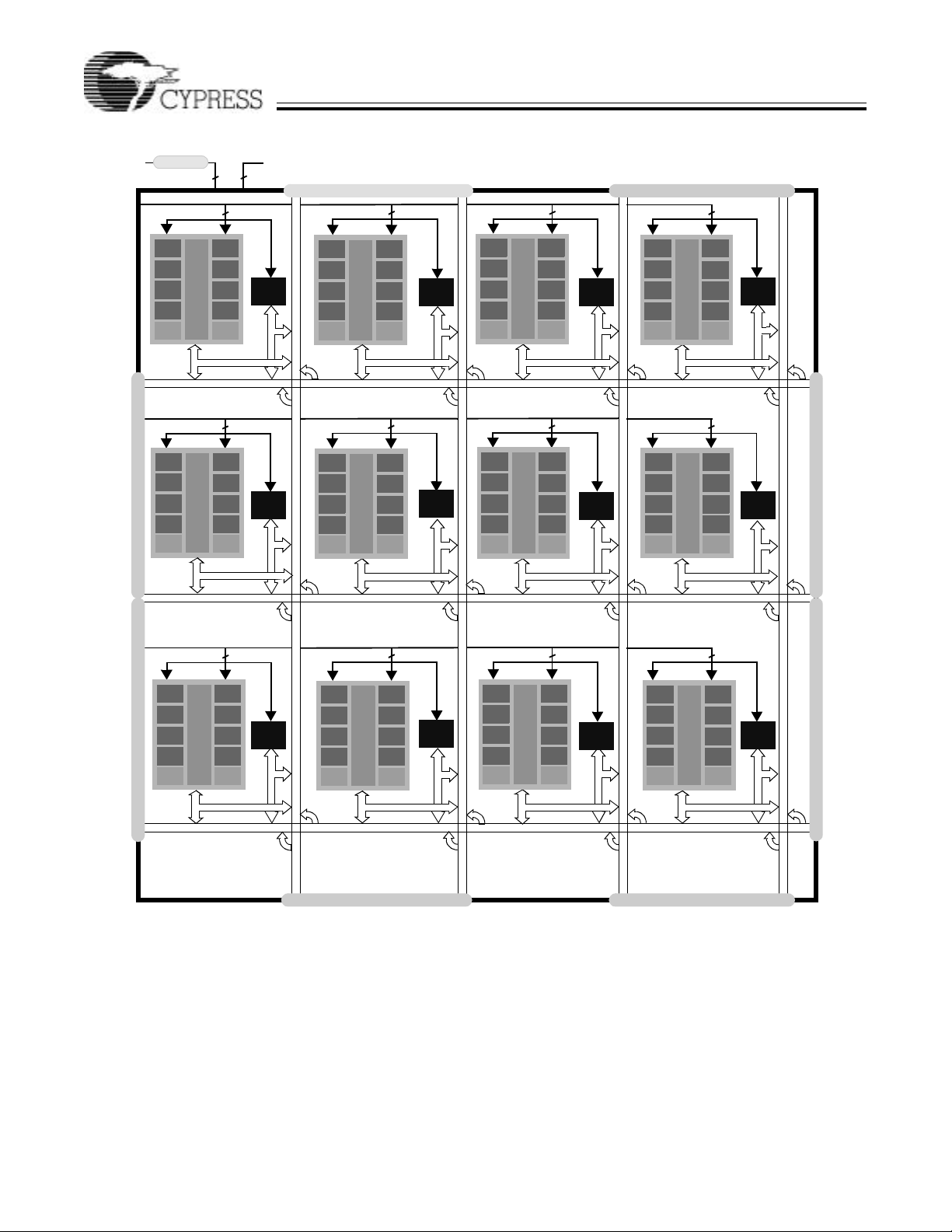
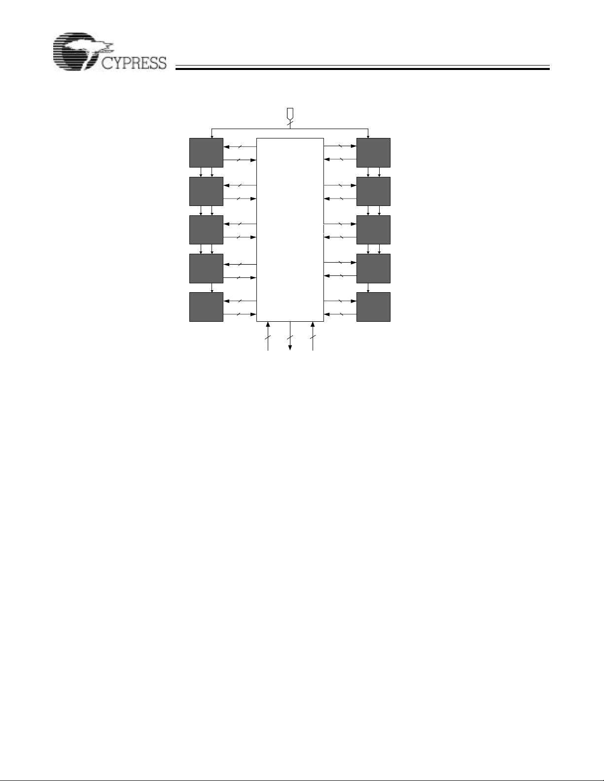
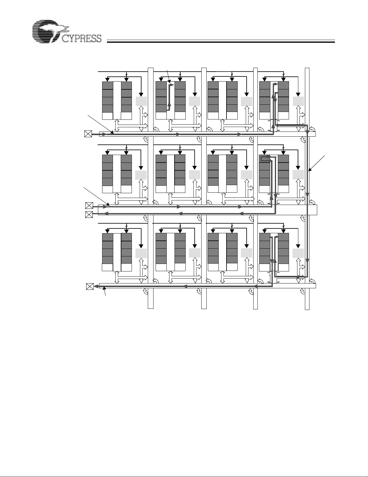
Figure 1. Delta39K100 Block Diagram (Three Rows × Four Columns) with I/O Bank Structure
General Description
The Delta39K family, based on a 0.18-mm, six-layer metal
CMOS logic process, offers a wide range of high-density
solutions at unparalleled system performance. The Delta39K
family is designed to combine the high speed, predictable
timing, and ease of use of CPLDs with the high densities and
low power of FPGAs. With devices ranging from 30,000 to
200,000 usable gates, the family features devices ten times
the size of previously available CPLDs. Even at these large
densities, the Delta39K family is fast enough to implement a
fully synth esizable 64-bit, 66-MHz PCI core.
4
LB 0
LB 1
LB 2
Cluster
RAM
PIM
LB 7
LB 6
LB 5
LB 4LB 3
Cluster
RAM
Channel
RAM
LB 0
LB 1
LB 2
Cluster
RAM
PIM
LB 7
LB 6
LB 5
LB 4LB 3
Cluster
RAM
Channel
RAM
I/O Bank 4
I/O Bank 3I/O Bank 2
The architecture is based on Logic Block Clusters (LBC) that
are connected by Horizontal and Vertical (H and V) routing
channels. Each LBC features eight individual Logic Blocks
(LB) and two cluster memo ry b loc ks . Adj ac ent to eac h LBC i s
a channel memory block, w hich can be acces sed directly from
the I/O pins. Both types of memory blocks are highly configurable and can be c as ca ded i n w id t h and depth. See Figure 1
for a block diagram of the Delta39K architecture.
All the members of th e Delt a39K fa mi ly have C ypres s’ s hig hly
regarded In-System Reprogrammability (ISR) feature, which
simplifies both design and manufacturing flows, thereby
reducing costs. The ISR feature provides the ability to recon-
Document #: 38-03039 Rev. *H Page 3 of 86
Delta39K™ ISR
™
ly
figure the devices without having design changes cause
pinout or timing changes in most cases. The Cypress ISR
function is implemented through a JTAG-compliant serial
interface. Data is shifted in and out through the TDI and TDO
pins respectively. Superior routability, simple timing, and the
ISR allows users to chan ge exist ing logic de signs whil e simultaneously fixing pinout assignments and maintaining system
performance.
The entire family features JTAG for ISR and boundary scan,
and is compatible with the PCI Local Bus specification,
meeting the electrical and tim ing requirements. The Delt a3 9K
family also features user programmable bus-hold and slew
rate control capabilities on each I/O pi n.
AnyVolt Interface
All Delta39KV devices feature an on-chip regulator, which
accepts 3.3 V or 2.5V on the V
to 1.8V internally , the voltage level at which the core operate s.
supply pins and step s it down
CC
With Delta39K’s AnyVolt technology, the I/O pins can be
connected to either 1.8V, 2.5V, or 3.3V. All Delta39K devices
are 3.3V-tolerant regardless of V
or VCC settings.
CCIO
Table 1.
Device V
CC
39KV 3.3V or 2.5V 3.3V or 2.5V or 1.8V or 1.5V
V
CCIO
[5]
CPLD Fami
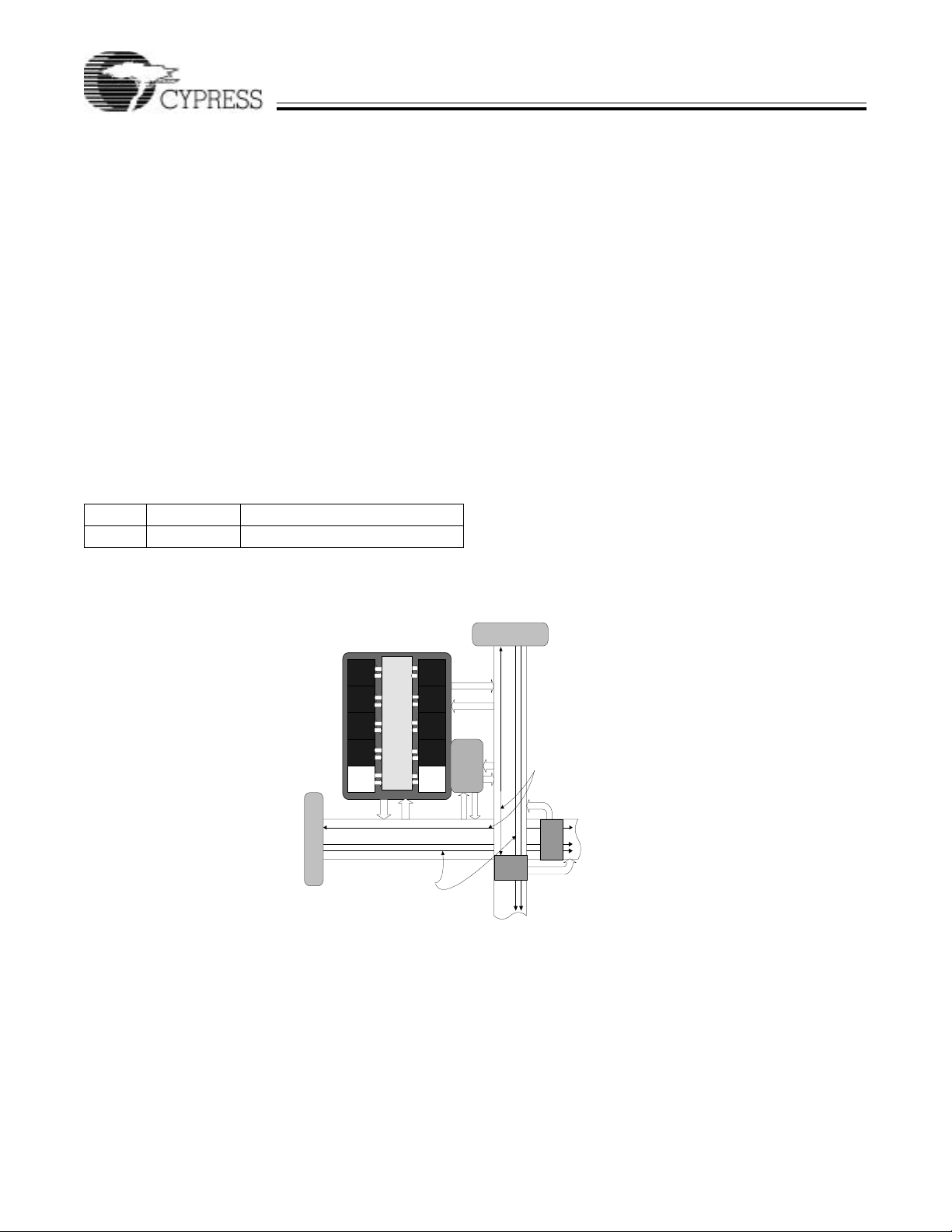
Global Routing Description
The routing architecture of the Delta39K is made up of
horizontal and vertical (H and V) routing channels. These
routing channels allow signals from each of the Delta39K
architectural com ponents to c ommunicate with on e another . In
addition to the horizontal and vertical routing channels that
interconnect the I/O ban ks, chann el memory bl ocks, and logi c
block clusters, each LBC contains a Programmable Interconnect Matrix (PIM™), which is used to route signals
among the logic blocks and the cluster memory blocks.
Figure 2 is a block diagram of the routing channels that
interface within the Del t a39 K arc hit ecture. The LBC is exactly
the same for every member of the Delta39K CPLD family.
Logic Block Cluster (LBC)
The Delta39K architecture consists of several logic block
clusters, each of which have eight Logic Blocks (LB) and two
cluster memory blocks connected via a Programmable Interconnect Matrix (PIM) as shown in Figure 3. Each cluster
memory block consists of 8-Kbit single-port RAM, which is
configurable as synchronous or asynchronous. The cluster
memory blocks can be cascaded with other cluster memory
blocks within the same LBC as well as other LBCs to
implement larger m emory func tions. If a clus ter me mory bloc k
is not specifically utilized by the designer, Cypress’s Warp
software can au tom ati ca lly us e it to implement large blo ck s of
logic.
All LBCs interface with each other via horizontal and vertical
routing channels.
Note:
5. For HSTL only.
I/O Block
Cluster
PIM
LB
72
LB
64
LB
LB
Channel
Memory
Cluster
Block
Memory
Block
64
LB
LB
LB
LB
Cluster
Memory
Block
72
I/O Block
Pin inputs from the I/O cells
drive dedicated tracks in the
horizontal and vertical routing
channels
Figure 2. Delta39K Routing Interface
Channel memory
outputs drive
dedicated tracks in the
horizontal and vertical
routing channels
H-to-V
PIM
V-to-H
PIM
Document #: 38-03039 Rev. *H Page 4 of 86
Delta39K™ ISR
™
ly
Clock Inputs
n
Logic
Block
0
CC CC CC
Logic
Block
1
Logic
Block
2
Logic
Block
3
Cluster
Memory
0
Horizontal Routing
36
16
36
16
36
16
36
16
25
8
64 Inputs From
Channel
GCLK[3:0]
4
PIM
144 Outputs to
Horizontal and Vertical
cluster-to-channel PIMs
Logic
36
Block
16
Logic
36
Block
16
Logic
36
Block
16
Logic
36
Block
16
Cluster
25
Memory
8
CC = Carry Chai
64 Inputs From
Vertical Routing
Channel
CPLD Fami
7
CC CC CC
6
5
4
1
Figure 3. Delta39K Logic Block Cluster Diagram
Logic Block
The LB is the basic buildin g block of the Delta 39K architecture.
It consists of a product term array, an intelligent product-term
allocator, and 16 macrocells.
Product Term Array
Each logic block features a 72 x 83 programmable product
term array. This array accepts 36 inputs from the PIM. These
inputs originate from device pins and macrocell feedbacks as
well as cluster memory and channel memory feedbacks.
Active LOW and active HIGH ver sions of each of thes e input s
are generated to create the full 72-input field. The 83 product
terms in the array can be created from any of the 72 inputs.
Of the 83 product terms, 80 are for general-purpose use for
the 16 macrocell s in the logic block. T wo of the remaining three
product terms in the logic bloc k are used as asynchro nous set
and asynchronous reset product te rms. The fi nal produc t term
is the Product Term clock (PTCLK) and is shared by all 16
macrocells within a logic block.
Product Term Allocator
Through the product term allocator, Warp software automatically distributes the 80 pro duct terms as needed amo ng the 16
macrocells in the logic block. The product term allocator
provides two important capabilities without affecting performance: product term steering and product term sharing.
Product Term Steering
Product term steering is the process of assigning product
terms to macroce lls as n eeded . For ex ampl e, if o ne macr ocell
requires ten product te rms whil e anoth er needs just thre e, the
product term allocator will “steer” ten product terms to one
macrocell and three to the other. On Delta39K devices,
product terms are stee red on an indivi dual ba sis. An y nu mber
between 1 and 16 product terms can be steered to any
macrocell.
Product Term Sharing
Product term sharing is the pr ocess of usin g the same product
term among multiple macrocell s. For example, i f more than
one function has one or more produ ct terms in it s equation th at
are common to other functions, those product terms are only
programmed once. The Delta39K product term allocator
allows sharing across groups of four macrocells in a variable
fashion. The software automatically takes advantage of this
capability so that the user does not have to intervene.
Note that neither product term sharing nor product term
steering have any effect on the speed of the product. All
steering and sharing c onfiguration s have been incorporated i n
the timing specifications for the Delta39K devices.
.
Document #: 38-03039 Rev. *H Page 5 of 86
Delta39K™ ISR
™
ly
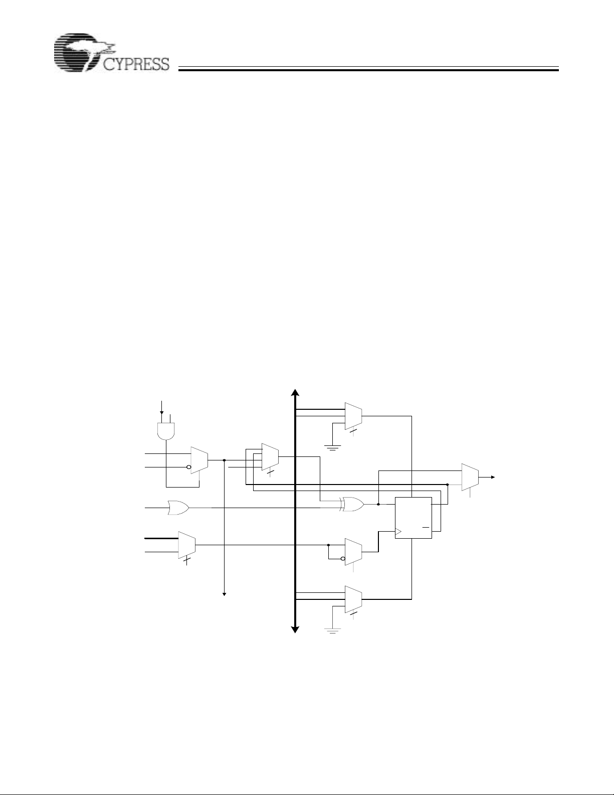
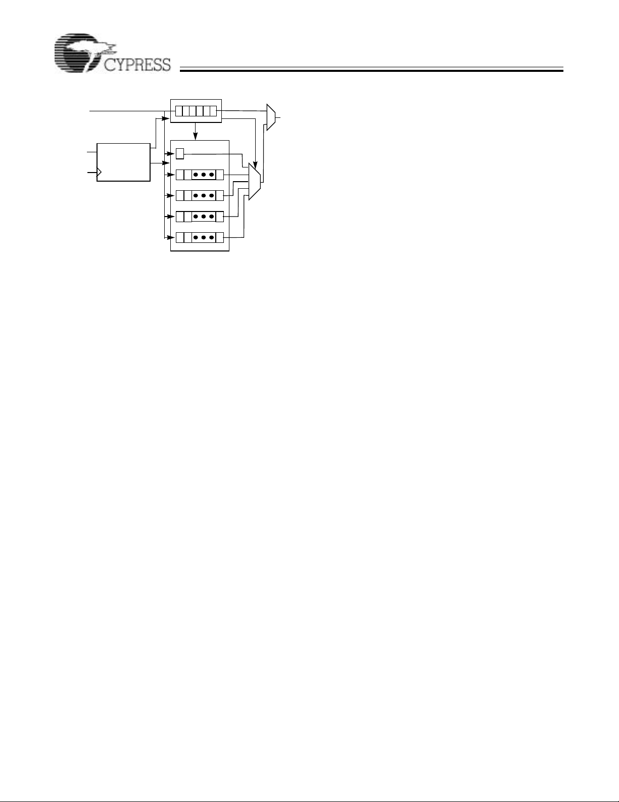
Macrocell
Within each logic block there are 16 macrocells. Each
macrocell accepts a sum of up to 16 product terms from the
product term array. The sum of these 16 product terms can be
output in either registered or combinatorial mode. Figure 4
displays th e b l oc k dia g r am of th e m ac r oc el l. T h e re g is t er c an
be asynchronously preset or asynchronously reset at the
macrocell level with the separate preset and reset product
terms. Each of these product terms features programmable
polarity. This allows the registers to be preset or reset based
on an AND expression or an OR expression.
An XOR gate in the Delta39K macrocell allows for many
different types of equations to be realized. It can be used as a
polarity mux to implement the true or complement form of an
equation in the product term array or as a to ggl e to tu rn the D
flip-flop into a T flip-flop. The carry-chain input mux allows
additional flexibil ity fo r the i mplem ent ation of dif fere nt type s of
logic. The macrocell can utilize the carry chain logic to
implement adders, subtractors, magnitude comparators,
parity tree, or even generic XOR logic. The output of the
macrocell is either registered or combinatorial.
Carry Chain Logic
The Delta39 K macrocell featu res carry chain l ogic which is
used for fast and eff ici en t imp lementation of arithmetic ope rations. The carry logic connects macrocells in up to four logic
blocks for a total of 64 macrocells. Effective data path opera-
CPLD Fami
tions are implemented through the use of carry-in arithmetic,
which drives through the circuit quickly. Figure 4 shows that
the carry chain logic within the macrocell consists of two
product terms (CPT0 and CPT1) from the PTA and an input
carry-in for carry logic. The inputs to the carry chain mux are
connected directly t o the produc t terms in the PTA. The output
of the carry chain mux generates the carry-out for the next
macrocell in the logic bl ock as wel l as the l ocal car ry inpu t that
is connected to an inp ut of the XOR input m ux. Carry-i n and a
configuration bit are inputs to an AND gate. This AND gate
provides a method of segmenting the carry chain in any
macrocell in the logic block.
Macrocell Clocks
Clocking of the register is highly flexible. Four global
synchronous clocks (GCLK[3:0]) and a PTCLK are available
at each macrocell register. Furthermore, a clock polarity mux
within each macrocell allows the register to b e clocked on the
rising or the falling edge (see macrocell diagram in Figure 4).
PRESET/RESET Configurations
The macrocell register can be asynchronously preset and
reset using the PRESET and RESET mux. Both signals are
active high and c an be controll ed by either o f two Preset/Res et
product terms (PRC[1:0] in Figure4) or GND. In situations
where the PRESET and RESET are active at the same time,
RESET takes priority over PRESET.
(from macrocell n-1)
CPT0
CPT1
FROM PTM
Up To 16 PTs
GCLK[3:0]
PTCLK
Carry In
Clock Mux
C
Carry Chain
Mux
3
C
Carry Out
(to macrocell n+1)
PRESET
0
1
XOR Input
Mux
C
2
C
PRC[1:0]
0
1
Mux
3
C
Clock
Polarity
Mux
C
3
C
RESET
Mux
Output
Mux
To PIM
PSET
D
Q
Q
RES
C
Figure 4. Delta39K Macrocell
Document #: 38-03039 Rev. *H Page 6 of 86
Delta39K™ ISR
™
ly
Embedded Memory
Each member of the Delta39K family contains two types of
embedded memory blocks. The channel memory block is
placed at the intersection of horizontal and vertical routing
channels. Each chan nel memor y block is 4096 bit s in size an d
can be configured as asynchrono us or synchro nous Dual- Port
RAM, Single-Port RAM, Read-Only memory (ROM), or
synchronous FIFO memory. The memory organization is
configurable as 4K × 1, 2K × 2, 1K × 4 and 512K × 8. The
second type of memory block is located within each LBC and
is referred to as a cluster memory block. Each LBC contains
two cluster memory blocks that are 8192 bits in size. Similar
to the channel memor y blocks, the c luster memory blocks ca n
be configured as 8K × 1, 4K × 2, 2K × 4 and 1K × 8
asynchronous or synchronous Single-Port RAM or ROM.
Cluster Memory
Each logic blo ck clu ster o f the Delt a39 K cont ain s two 8192-b it
cluster memory blocks. Figure 5 is a block diagram of the
cluster memory block and the interface of the cluster memory
block to the cluster PIM.
The output of the c luster memory block c an be optionally re gistered to perform synchronous pipelining or to register
asynchronous Read and Write operations. The output
registers contain an as ynchronous RESET which can be use d
in any type of sequential logic circuits (e.g., state machines).
There are four global clocks (GCLK[3:0]) and one local clock
available for the i nput and t he out put regis ters. The l ocal cloc k
for the input registers is independent of the one used for the
output registers. The local clock is generated in the user
design in a macrocell or comes from an I/O pin.
CPLD Fami
Cluster Memory Initialization
The cluster memory po wers up in an undefined st ate, but is set
to a user-defined k nown state durin g configuration. T o facilit ate
the use of look-up-t able (LUT) logic and ROM applications, th e
cluster memory blocks can be initialized with a given set of
data when the device is configured at power up. For LUT and
ROM applications, the user cannot write to memory blocks.
Channel Memory
The Delta39K architecture includes an embedded memory
block at each crossing point of horizontal and vertical routing
channels. The channel memory is a 4096-bit embedded
memory block that can be configured as asynchronous or
synchronous single-port RAM, dual-port RAM, ROM, or
synchronous FIFO memory.
Data, address, and control inputs to the channel memory are
driven from horizontal and vertical routing channels. All data
and FIFO logic output s drive dedicated trac ks in the horizont al
and vertical routing channels. The clocks for the channel
memory bloc k are selected from f our global clocks a nd pin
inputs from the horizontal and vertical channels. The clock
muxes also inc lude a p olarity mux for e ach clock s o that t he
user can choose an inverted clock.
Dual-Port (Channel Memory) Configuration
Each port has distinct addre ss inputs, as wel l as separate dat a
and control inputs that can be accessed simultaneously. The
inputs to the Dual-Port mem ory are driv en from the hori zont al
and vertical routing channels. The data outputs drive
dedicated tracks in the routing channels. The interface to the
routing is such that Port A of the Dual-Po rt interface s primarily
with the horizontal routing channel and Port B interfaces
primarily with the vertical routing channel.
2
Write
Control
Logic
8
C
1024x8
Asynchronous
SRAM
8
Cluster PIM
GCLK[3:0]
Local CLK
DOUT[7:0]
RESET
GCLK[3:0]
Local CLK
DIN[7:0]
ADDR[12:0]
WE
Read
Control
Logic
2
3
Row Decode (1024 Rows)
10
3
C
DQ
C
DQ
C
Pulse
Write
DQ
C
5:1
3
C
C
5:1
3
C
DQ
R
Figure 5. Block Diagram of Cluster Memory Block
Document #: 38-03039 Rev. *H Page 7 of 86
Delta39K™ ISR
™
ly
The clocks for each port of the Dual-Port configuration are
selected from four global clocks and two local clocks. One
local clock is sourced from the horizontal channel and the
other from the vertical channel. The data outputs of the dualport memory can also be registered. Clocks for the output
registers are also selected from four global clocks and two
local clocks. O ne c lo ck p ola rity m ux p er port al low s t he us e of
true or complement polarity for input and output clocking
purposes.
Arbitration
The Dual-Port configuration of the Channel Memory Block
provides arbitrat ion when bot h ports a ccess the sam e address
at the same time. Depending on the memory operation being
attempted, one port always gets priority. See Table 2 for
details on which port gets priority for Read and Write operations. An active-LOW “Address Match” signal is generated
when an address collision occurs.
Table 2. Arbitration Result: Address Match Signal
Becomes Active
Port A Port B
Read Read No arbitration
Write Read Port A gets
Read Write Port B gets
Write Write Port A gets
FIFO (Channel Memory) Configuration
The channel memory blocks are also configurable as
synchronous FIFO RAM. In the FIFO mode of operation, the
channel memory block supports all normal FIFO operations
without the use of any general-purpose logic resources in the
device.
Result of
Arbitration Comment
Both ports read at the
required
priority
priority
priority
same time
If Port B requests first then
it will read the current
data. The output will then
change to the newly
written data by Port A
If Port A requests first then
it will read the current
data. The output will then
change to the newly
written data by Port B
Port B is blocked until Port
A is finished writing
The FIFO block contains all of the necessary FIFO flag logic,
including the Read an d Write address poi nters. The FIFO flags
include an empty/ful l flag (EF
mable almost-empty /ful l (PAEF
uration has the ab ility to perform simultaneo us Read and W rite
operations using two separate clocks. These clocks may be
tied together for a single operation or may run independently
for asynchronous Re ad/Write (with re gard to each other) appl ications. The data and control inputs to the FIFO block are
driven from the horizontal or vertical routing channels. The
data and flag o utpu t s are driv en onto dedicated routing trac k s
in both the horizont al and vertical routing channels . This allows
the FIFO blocks to be exp anded by using multipl e FIFO bloc ks
on the same horizon tal or vertical rout ing ch annel without any
speed penalty.
In FIFO mode, the Write and Read ports are controlled by
separate clock and enable signals. The clocks for each port
are selected from four global clocks and two local clocks.
One local clock is sourced from the horizont al channel an d the
other from the vertical channel. The data outputs from the
Read port of the FIFO can also be registered. One clock
polarity mux per port allo ws using true or com plem ent pol arity
for Read and Write operations. The Write operation is
controlled by the clock and the Write enable pin. The Read
operation is controlled by the clock and the Read enable pin.
The enable pins can be sourced from horizontal or vertical
channels.
Channel Memory Initialization
The channel memory powers up in an undefined state, but is
set to a user-defined known state du ring configuration. T o faci litate the use of look-up-table (LUT) logic and ROM applications, the channel memory blocks can be initialized with a
given set of data when the device is configured at power up.
For LUT and ROM applications, the user cannot write to
memory blocks.
Channel Memory Routing Interface
Similar to LBC outputs, the channel memory blocks feature
dedicated tracks in the hori zontal and vertical routing channels
for the data outputs and the flag outputs, as shown in
Figure 6. This allows the channel memory blocks to be
expanded easi ly. These dedic ated li nes can b e route d to I/O
pins as chip outputs or to other logic block clusters to be used
in logic equations.
), half-full flag (HF), an d program-
CPLD Fami
) flag output. The FIFO confi g-
Document #: 38-03039 Rev. *H Page 8 of 86
Delta39K™ ISR
™
ly
All channel memory
k
inputs are driven from
the routing channels
4096-bit Dual-Port
Array
Configurable as
Async/Sync Dual-Port
or Sync FIFO
Configurable as
4K x 1, 2K x 2, 1K x 4,
and 512 x 8 block sizes
All channel memory outputs
drive dedicated tracks in the
routing channels
Horizontal Channel
Figure 6. Block Diagram of Channel Memory Block
Vertical Channel
CPLD Fami
Global Cloc
Signals
GCLK[3:0]
I/O Banks
The Delta39K interfaces the horizontal and vertical routing
channels to the pins through I/O banks. There are eight I/O
banks per device as shown in Figure 7, and all I/Os from an
I/O bank are loca ted in the sam e section o f a packa ge for PCB
layout convenience.
Delta39K devices support True Vertical Migration™ (i.e., for
each package type, Delta39K devices of different densities
keep given pins in the same I/O banks). This allows for easy
and simple im plementation o f multiple I/O s tandards during the
design and proto typ ing ph ase, before a final dens ity h as bee n
determined. Please refer to the application n ote titl ed “Family,
Package and Densi ty Migration in Delt a 39K and Quantum3 8K
CPLDs.”
Each I/O bank contain s several I/O cells, and each I/O ce ll
contains an input/output register, an output enable register,
programmabl e slew rate contr ol and progr ammabl e bus h old
control logic. Each I/O cell drives a pin output of the device;
the cell also suppli es an i npu t to the d ev ic e tha t c onn ec ts to a
dedicated track in the assoc ia ted rout ing channel.
Each I/O bank can use any supported I/O standard by
supplying appropriate V
uring the I/O through the Warp software. All the V
V
and V
number of I/O standards sup ported by an I/O bank at any given
time.
The number of I/Os which can be used in each I/O bank
depend on the type of I/O s tand ards an d the num ber of V
and GND pins being used. This restriction is derived from the
electromigration limit of the V
chip. Please refer to the note on page 17 and the application
note titled “Delta39K Fam ily Device I/ O St andards and Config-
urations” for details.
and V
REF
pins in an I/O bank must be connected to the same V
CCIO
voltage respectively. This requirement restricts the
CCIO
CCIO
voltages and con fig-
CCIO
and GND bussing on the
REF
and
REF
CCIO
I/O Cell
Figure 8 is a block diagram of the Delta39K I/O cell. The I/O
cell contains a thre e-s t ate inp ut bu ffer, an outp ut bu ffer, an d a
register that can be configured as an input or output register.
The output b uffer has a sl ew rate cont rol option that can be
used to configure the output for a slower slew rate. The input
of the device and the pin output can each be configured as
registered or combinatorial; however, only one path can be
configured as registered in a given design.
The output enable in an I/O cell can be selected from one of
the four global control signals or from one of two Output
Control Channel (OCC) signals. The output enable can be
configured as always enabled or always disabled or it can be
controlled by one of the remaining inputs to the mux. The
selection is done via a mux that includes V
inputs.
and GND as
CC
bank 6bank 7
bank 0bank 1
Delta39K
Delta39K
bank 4 bank 5
bank 2 bank 3
Figure 7. Delta39K I/O Bank Block Diagram
Document #: 38-03039 Rev. *H Page 9 of 86
Delta39K™ ISR
™
ly
From
Output PIM
To Routing
Channel
Registered OE
OE Mux
DQ
3
C
Clock
Polarity
Mux
C
C
Register Input
Mux
DQ
E
RES
Output Mux
C
Input
Mux
Global Clock Signals
Global I/O Control Signals
Output Control Channel OCC
C
Register Enable
Mux
3
C
Clock Mux
2
C
Register Reset
Mux
3
C
Mux
C
RES
Bus
Hold
C
Slew
Rate
Control
C
CPLD Fami
I/O
Figure 8. Block Diagram of I/O Cell
I/O Signals
There are four dedicated inputs (GCTL[3:0]) that are used as
Global I/O Control Signals available to every I/O cell. These
global I/O control signals may be used as output enables,
register resets and register clock enables as shown in
Figure 8. These global control signals, driven from four
dedicated pins, can only be used as active-high signals and
are available only to the I/O cells thereby implementing fast
resets, register and output enables.
In addition, there are six OCC signals available to each I/O
cell. These control signals may be used as output enables,
register resets and register clock enables as shown in
Figure 8. Unlike global control signals, these OCC signal can
be driven from internal logic or and I/O pin.
One of the four global clocks can be selected as the clock for
the I/O cell regi ster . The c lock mux out put is an input to a cl ock
polarity mux that all ows the input /output register to be c locked
on either edge of the clock
Slew Rate Control
The output buffer has a slew rate control option. This allows
the output buffer to slew at a fast rate (3 V/ns) or a slow rate
(1 V/ns). All I/Os default to fast slew rate. For designs
concerned with meeting FCC emissions standards the slow
edge provides for lower system noise. For designs requiring
very high performance the fast edge rate provides maximum
system performance.
Table 3.
I/O Standards
I/O
Standard V
(V) V
REF
CCIO
Termination
Voltage (VTT)
Min. Max.
LVTTL N/A 3.3V N/A
LVCMOS 3.3V N/A
LVCMOS3 3.0V N/A
LVCMOS2 2.5V N/A
LVCMOS18 1.8V N/A
3.3V PCI 3.3V N/A
GTL+ 0.9 1.1 N/A 1.5
SSTL3 I 1.3 1.7 3.3V 1.5
SSTL3 II 1.3 1.7 3.3V 1.5
SSTL2 I 1.15 1.35 2.5V 1.25
SSTL2 II 1.15 1.35 2.5V 1.25
HSTL I 0.68 0.9 1.5V 0.75
HSTL II 0.68 0.9 1.5V 0.75
HSTL III 0.68 0.9 1.5V 1.5
HSTL IV 0.68 0.9 1.5V 1.5
Document #: 38-03039 Rev. *H Page 10 of 86
Delta39K™ ISR
™
ly
G
0
Programmable Bus Hold
On each I/O pin, user-programmable-bus-hold is included.
Bus-hold, which is an improved version of the popular internal
pull-up resistor, is a weak latch connected to the pin that does
not degrade the device’s performance. As a latch, bus-hold
maintains the last state of a pin when the pin is placed in a
high-impedance state, thus reducing system noise in businterface applications. Bus-hold additionally allows unused
device pins to remain unconnected on the board, which is
particularly useful during prototyping as designers can route
new signals to the device with out cutti ng trac e co nne ctions to
or GND. For more information, see the application note
V
CC
titled “Understanding Bus-Hold–A Feature of Cypress
CPLDs.”
Clocks
Delta39K has four dedicated clock input pins (GCLK[3:0]) to
accept system clocks. One of these clocks (GCLK[0]) may be
selected to drive an on-chip phase-locked loop (PLL) for
frequency modulation (see Figure 9 for details).
The global clock tree for a Delta39K device can be driven by
a combination of the dedicated clock pins and/or the PLLderived clocks. The global clock tree consists of four global
clocks that go to e ve ry m ac roc el l, m em ory b loc k, and I/O cell.
Clock Tree Distribution
The global clock tree performs two prima ry functions. Firs t, the
clock tree generates the fou r global clocks by mult iplexing four
dedicated clocks from the package pins and four PLL driven
clocks. Second, the clo ck tree distributes the fo ur global clocks
to every cluster, channel memory, and I/O block on the die.
The global clock tree is designed such that the clock skew is
minimized while maintaining an acceptable clock delay.
Spread Aware PLL
Each device in the Delta39K family features an on-chip PLL
designed using S pre ad Aware t echnology for lo w EMI applications. In general, PLLs are used to implement time-divisionmultiplex circuits to achieve higher performance with fewer
device resources.
off-chip signal (external feedback)
INTCLK0, INTCLK1, INTCLK2, INTCLK3
GCLK1
Clock Tree
Delay
2
C
fb
GCLK0
Source
Clock
PLL
X1, X2, X3, X4, 5X,
X6, X8, X16
CLK[3:0]
fb
Lock
Clk
0
0
0
Clk 45
Clk
0
90
0
Clk 135
0
Clk 180
Clk
0
225
Clk
0
270
Clk
0
315
Figure 9. Block Diagram of Spread Aware PLL
Phase selection
Phase selection
Phase selection
Phase selection
CPLD Fami
For example, a system th at operates on a 32-bit dat a path th at
runs at 40 MHz can be implemented with 16-bit circuitry that
runs internally at 80 MHz. PLLs can also be used to take
advantage of the positioning of the internally generated clock
edges to shift performance towards improved setup, hold or
clock-to-out times.
There are several freq uen cy multi pl y (X1 , X2 , X3, X4, X5, X6,
X8, X16) and divide (/1, /2, /3, /4, /5, /6, /8, /16) options
available to create a wide range of clock frequencies from a
single clock input (GCLK[0 ]). For increased flexibility , there are
seven phase shifting options which allow clock skew/deskew
by 45°, 90°, 135°, 180°, 225°, 270°, or 315°.
The Spread Aware feature refers to the ability of the PLL to
track a spread-spectrum input clock such that its spread is
seen on the outp ut clock wi th the PLL s taying l ocked. The total
amount of spread on th e inpu t clock shou ld be li mited to 0.6 %
of the fundamental frequency. Spread Aware feature is
supported only with X1, X2, and X4 multiply options.
The Voltage Controlled Oscillator (VCO), the core of the
Delta39K PLL is designed to operate within the frequency
range of 100 MHz to 266 MHz. Hence, the multiply option
combined with input (GCLK[0]) frequency should be selected
such that this VCO operating frequency requirement is met.
This is demonstrated in Table 4 (columns 1, 2, and 3).
Another feature of this PLL is the ability to drive the output
clock (INTCLK) of f the Delt a39K chip to clock o ther devi ces on
the board, as shown in Figure 9 above. This off-chip clock is
half the frequency o f the out put clo ck as it h as to go through a
register (I/O register or a macrocell register).
This PLL can also be used for board de-skewing purpose by
driving a PLL output clock off-chip, routing it to the other
devices on the board and feed ing it ba ck to the PLL’s external
feedback input (GCLK[1]). When this feature is used, only
limited multiply, divide and phase shift options can be used.
Table 4 describes the valid multiply and d ivide option s that can
be used without extern al feedback. Table 5 describes the valid
multiply and divide options that can be used with an external
feedback.
Normal I/O signal path
Any Register (TFF)
Divide
¸ 1-6,8,16
Divide
¸ 1-6,8,16
Divide
¸ 1-6,8,16
Divide
¸ 1-6,8,16
Send a global clock off
chip
Lock Detect/IO pin
C
GCLK0
2
GCLK1
2
GCLK2
2
GCLK3
2
INTCLK
C
INTCLK1
C
INTCLK2
C
INTCLK3
C
Document #: 38-03039 Rev. *H Page 11 of 86
Delta39K™ ISR
™
ly
Table 6 describes the valid phase shift options that can be
used with or without an external feedback.
Table 7 is an example of the effect of all the available divide
and phase shift options on a VCO output of 250 MHz. It also
shows the effect of division on the duty cycle of the resultant
clock. Note that the duty cycle is 50-50 when a VCO output is
divided by an even number. Also note that the phase shift
applies to the VCO output and not to the divided output.
Table 4. Valid PLL Multiply and Divide Options—without External Feedback
Input Frequency
(GCLK[0])
(MHz)
f
PLLI
DC–12.5 N/A N/A N/A DC–12.5 DC–6.25
100–133 1 100–133 1–6, 8, 16 6.25–133 3.125–66
50–133 2 100–266 1–6, 8, 16 6.25–266 3.125–133
33.3–88.7 3 100–266 1–6, 8, 16 6.25–266 3.1–266
25–66 4 100–266 1–6, 8, 16 6.25–266 3.125–133
20–53.2 5 100–266 1–6, 8, 16 6.25–266 3.1–133
16.6–44.3 6 100–266 1–6, 8, 16 6.25–266 3.1–133
12.5–33 8 100–266 1–6, 8, 16 6.25–266 3.125–133
12.5–16.625 16 200–266 1–6, 8, 16 6.25–266 3.125–133
Valid Multiply Options Valid Divide Options
Value
VCO Output
Frequency (MHz) Value
For more details o n th e arc hi tec ture an d o pera tio n of thi s PL L
please refer to the applicat ion note entitled “Delta3 9K PLL and
Clock Tree”.
Output Frequency (INTCLK[3:0])
f
PLLO
(MHz)
CPLD Fami
Off-chip Clock
Frequency
Table 5. Valid PLL Multiply and Divide Options—With External Feedback
Valid Multiply Options Valid Divide Options
Input (GCLK) Frequency
50–133 1 100–266 1 100–266 50–133
25–66.5 1 100–266 2 50–133 25–66.5
16.67–44.33 1 100–266 3 33.33–88.66 16.67–44.33
12.5–33.25 1 100–266 4 25–66.5 12.5–33.25
12.5–26.6 1 125–266 5 25–53.2 12.5–26.6
12.5–22.17 1 150–266 6 25–44.34 12.5–22.17
12.5–16.63 1 200–266 8 25–33.25 12.5–16.63
Table 6. Recommended PLL Phase Shift Options
0°,45°, 90°, 135°, 180°, 225°, 270°, 315° 0°
Table 7. Timing of Clock Phases for all Divide Options for a V
Divide
Factor
1 4 40–60 0 0.5 1.0 1.5 2.0 2.5 3.0 3.5
2 8 50 0 0.5 1.0 1.5 2.0 2.5 3.0 3.5
3 12 33–67 0 0.5 1.0 1.5 2.0 2.5 3.0 3.5
4 16 50 0 0.5 1.0 1.5 2.0 2.5 3.0 3.5
5 20 40–60 0 0.5 1.0 1.5 2.0 2.5 3.0 3.5
6 24 50 0 0.5 1.0 1.5 2.0 2.5 3.0 3.5
8 32 50 0 0.5 1.0 1.5 2.0 2.5 3.0 3.5
16 64 50 0 0.5 1.0 1.5 2.0 2.5 3.0 3.5
(MHz)
f
PLLI
Period
(ns) Duty Cycle%0°(ns)
Value
Without External Feedback With External Feedback
VCO Output
Frequency (MHz) Value
CO
45°
(ns)
90°
(ns)
Output (INTCLK) Frequency
Output Frequency of 250 MHz
135°
(ns)
180°
(ns)
f
PLLO
(MHz)
225°
(ns)
Off-chip Clock
Frequency
270°
(ns)
315°
(ns)
Document #: 38-03039 Rev. *H Page 12 of 86

Delta39K™ ISR
™
ly
CompactPCI Hot Swap
The CompactPCI Hot Swap specification allows the removal
and insertion of cards into CompactPCI sockets without
switching-off the bus. Delta39K CPLDs can be used as a
CompactPCI host or target on these cards.
This feature is useful in telecommunication and networking
applications as it allows implementation of high availability
systems, where repairs and upgrades can be done without
downtime.
Delta39K CPLDs are CompactPCI Hot Swap Ready per
CompactPCI Hot Swap specification R2.0, with the following
exception:
• The I/O cells do not provide bias voltage support. External
resistors can be used to achieve this, per sectio n 3.1.3.1 of
the CompactPCI Hot Swap specification R2.0. A simple
board level sol ution is prov ided in the ap plication note titled
“Hot-Swapping Delta39K and Quantum38K CPLDs.”
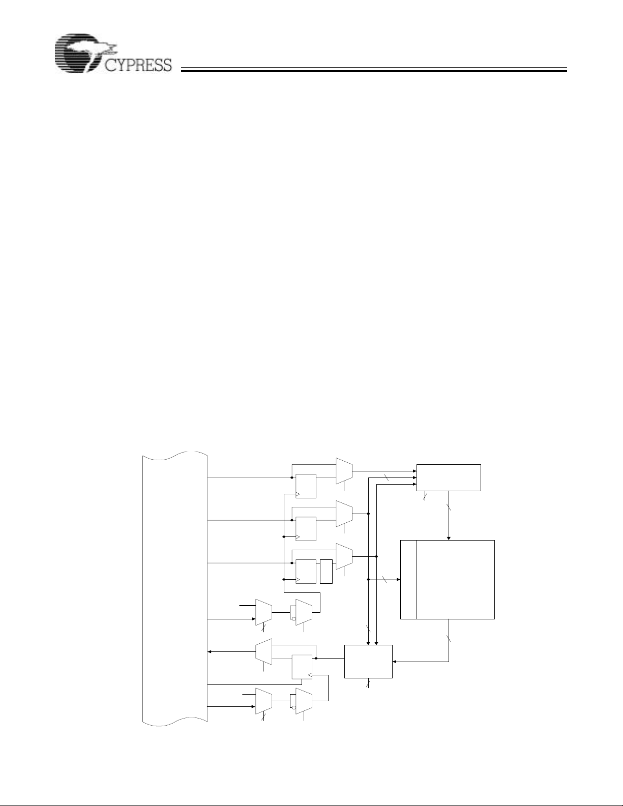
Timing Model
One important feature of the Delta39K family is the simplicity
of its timing. All combinatorial and registered/synchronous
delays are worst case and system performance is static (as
shown in the AC specs section) as long as data is routed
through the same horizontal and vertical channels. Figure 10
illustrates the true timing model for the 200-MHz devices. For
synchronous cloc king of macroc ells, a del ay is i ncurr ed from
macrocell cloc k to macrocell clock o f separate Logic Blocks
within the same cluster, as well as separate Logic Blocks
within differe nt clusters. This is respectively shown as t
t
in Figure 10. For combinatorial paths, any input to any
SCS2
SCS
and
output (from corner to corner on the device), incurs a worstcase delay in the 3 9K100 regardless of the amo unt of l ogic or
which horizontal and vertical channels are u sed. This is the t
shown in Figure 10. For synchronous systems, the input setup time to the outp ut macrocel l register and the clock to o utput
time are shown as the parameters t
the Figure 10. These measurements are for any output and
synchronous clock, regardless of the logic placement.
The Delta39K features:
• no dedicated vs. I/O pin delays
• no penalty for using 0 – 16 product terms
• no added delay for steering product terms
• no added delay for sharing product terms
• no output bypass delays.
The simple timing model of the Delta39K family eliminates
unexpected performance penalties.
Family, Package, and Density Migration in Delta39K
CPLDs
The Delta39K CPLDs combine dense logic, embedded memory and configurable I/O standards. Further de sign flexibil ity is
added by the easy m igra tio n options available be tw een d if f erent packages and densities of Delta39K CPLD offerings.
This migration flexibility makes changes or additions to
designs simple even after PCB layout. It also provides the
ability for experimental designs to be used on production
PCBs. Please refer to the application note titled “Family,
Package, and Density Migration in Delta39K CPLDs.”
CPLD Fami
MCS
and t
MCCO
shown in
PD
Document #: 38-03039 Rev. *H Page 13 of 86
Delta39K™ ISR
™
ly
t
t
MCS
PD
GCLK[3:0]
PIM
PIM
LB 7
LB 6
LB 5
LB 4
RAM
LB 7
LB 6
LB 5
LB 4
Cluster
RAM
LB 0
LB 1
LB 2
LB 3
Cluster Cluster
RAM
GCLK[3:0]
LB 0
LB 1
LB 2
LB 3
Cluster
RAM
4
4
Channel
RAM
Channel
RAM
t
SCS
LB 0
LB 1
LB 2
LB 3
Cluster
RAM
LB 0
LB 1
LB 2
LB 3
Cluster
RAM
PIM
PIM
LB 7
LB 6
LB 5
LB 4
Cluster
RAM
LB 7
LB 6
LB 5
LB 4
Cluster
RAM
4
4
Channel
Channel
RAM
RAM
LB 0
LB 1
LB 2
LB 3
Cluster
RAM
LB 0
LB 1
LB 2
LB 3
Cluster
RAM
PIM
PIM
LB 7
LB 6
LB 5
LB 4
Cluster
RAM
LB 7
LB 6
LB 5
LB 4
Cluster
RAM
4
4
Channel
RAM
Channel
RAM
CPLD Fami
4
LB 0
LB 1
LB 2
LB 3
SRAM
LB 0
LB 1
LB 2
LB 3
Cluster
RAM
8 Kb
PIM
PIM
LB 7
LB 6
LB 5
LB 4
8 Kb
SRAM
LB 7
LB 6
LB 5
LB 4
Cluster
RAM
4
Channel
RAM
Channel
RAM
t
SCS2
GCLK[3:0]
LB 0
LB 1
LB 2
LB 3
Cluster
RAM
t
MCCO
PIM
LB 7
LB 6
LB 5
LB 4
Cluster
RAM
4
Channel
RAM
LB 0
LB 1
LB 2
LB 3
Cluster
RAM
PIM
Figure 10. Timing Model for 39K100 Device
IEEE 1149.1-compliant JTAG Operation
The Delta39K family has an IEEE 1149.1 JTAG interface for
both Boundary Scan and ISR operations.
Four dedicated pins are reserved on each device for use by
the Test Access Port (TAP).
Boundary Scan
The Delta39K family supports Bypass, Sample/Preload,
Extest, Intest, Idcode and Usercode boundary scan instructions. The JTAG interface is shown in Figure 11.
In-System Reprogramming (ISR)
In-System Reprogram ming is the combi nation of the cap ability
to program or reprogram a device on-board, and the ability to
support design changes without changing the system timing
or device pinout. This combination means design changes
during debug or field upgrades do not cause board respins.
LB 7
LB 6
LB 5
LB 4
Cluster
RAM
4
Channel
RAM
LB 0
LB 1
LB 2
LB 3
Cluster
RAM
PIM
LB 7
LB 6
LB 5
LB 4
Cluster
RAM
4
Channel
RAM
LB 0
LB 1
LB 2
LB 3
Cluster
RAM
PIM
LB 7
LB 6
LB 5
LB 4
Cluster
RAM
4
Channel
RAM
The Delta39K family implements ISR by providing a JTAG
compliant int e rf ac e f or on -bo a rd p r ogr a mmi ng, r obu st ro ut i ng
resources for pinout flexibility, and a simple timing model for
consistent system performance.
Configuration
Each device of the Delta39K fa mily is available in a volatile an d
a Self-Boot package . Cypres s’s CPLD boot EEPROM is used
to store configuration data for the volatile solution and an
embedded on-chip FLASH m emory device is used for th e SelfBoot solution.
For volatile Delta39K packages, programming is defined as
the loading of a user’s design into the external CPLD boot
EEPROM. For Self-Boot Delta39K packa ges, program ming is
defined as the loading of a user’s design into the on-chip
FLASH internal to the Delta39K package. Configuration is
defined as the load ing of a user’s design int o the Delta39 K die.
Document #: 38-03039 Rev. *H Page 14 of 86
Delta39K™ ISR
™
ly
Instruction Register
O
TDI
TMS
TCLK
Configuration can begin in two ways. It can be initiated by
toggling the Reconfig pin from LOW to HI GH, or by issuing th e
appropriate IEEE STD 1149.1 JTAG instruction to the
Delta39K device via the JTAG interface. There are two IEEE
STD 1149.1 JTAG instructions that initiate configu rati on of th e
Delta39K. The Self Config instruction causes the Delta39K to
(re)configure with data stored in the serial boot PROM or the
embedded FLASH memory. The Load Config instruction
causes the Delta39K to (re)configure according to data
provided by other sources such as a PC, automatic test
equipment (ATE), or an embedded micro-controller/pro cess or
via the JTAG interface. For more informatio n on configuring
Delta39K devices, refer to the application note titled “Config-
uring Delta39K/Quantum38K” at http://www.cypress.com.
There are two configuration options available for issuing the
IEEE STD 1 149. 1 JTAG instructions to the Delta39K. Th e first
method is to use a PC with the C3ISR programming cable and
software. With this method, the ISR pins of the Delta39K
devices in th e sys tem are rou ted to a co nnecto r a t the edg e of
the printed circuit board. The C3ISR programming cable is
then connected between the PC and this connector. A simple
configuration file instructs the ISR software of the
programming operations to be performed on the Delta39K
devices in the system. The ISR software then automatically
completes all of the necessary data manipulations req uir ed to
accomplish configuration, reading, verifying, and other ISR
functions. For more i nform at ion on the Cypress ISR i nterface,
see the ISR Programming Kit data sheet (CY3900i).
The second configuration option for the Delta39K is to utilize
the embedded contr oller or proc essor that alrea dy exists i n the
system. The Delta3 9K ISR soft war e as si sts in th i s me tho d by
converting the device HEX file into the ISR serial stream that
contains the ISR instruction information and the addresses
and data of locations to be configured. The embedded
controller then simply directs this ISR stream to the chain of
JTAG
TAP
CONTROLLER
Figure 11. JTAG Interface
Bypass Reg.
Boundary Scan
idcode
Usercode
ISR Prog.
Data Registers
TD
Delta39K devices to complete the desired reconfiguration or
diagnostic operat ions. Cont act y our loc al sa les o f fice for inf ormation on the availability of this option.
Programming
The on-chip FLASH device o f the Delta39K Se lf-Boot package
is programmed by issuing the appropriate IEEE STD 1149.1
JTAG instruction to the internal FLASH memory via the JTAG
interface. This can be done automatically using ISR/STAPL
software. The configuration bits are sent from a PC through
the JTAG port into the Delta39K via the C3ISR programming
cable. The dat a is th en int ernally p assed from De lt a39K t o the
on-chip FLASH. For more information on how to program the
Delta39K through ISR/STAPL, please refer to the ISR/STAPL
User Guide.
The external CPLD boot EEPROM used to store confi guration
data for the Delt a39K vo latile pa ckage is progr ammed throug h
Cypress’s CYDH2200E CPLD Boot PROM Programming Kit
via a two-wire interface. For more information on how to
program the CPLD boot EEPROM, please refer to the data
sheet titled “CYDH2200E CPLD Boot PROM Programming
Kit.” For more information o n the architecture and tim ing specification of the boot EEPROM, refer to the data sheet titled
“512K/1Mb CPLD Boot EEPROM” or “2-Mbit CPLD Boot
EEPROM.”
Third-Party Programmers
Cypress support is available on a wide variety of third-party
programmers. All major programmers (including BP Micro,
System General, Hi-Lo) support the Delta39K family.
CPLD Fami
Development Software Support
Warp
Warp is a state-of-the-art desig n environment for design ing
with Cypress programmable logic. Warp utilizes a subset of
IEEE 1076/1164 VHDL and IEEE 1364 as the Hardware
Description Language (HDL) for design entry. Warp accepts
VHDL or Veri log inpu t, synth esize s and opti mize s the entere d
design, and outputs a configuration bitstream for the desired
Delta39K device. For simulation, Warp provides a graphical
waveform simulator as well as VHDL and Verilog Timing
Models.
VHDL and Verilog are open, powerful, non-proprietary
Hardware Description Languages (HDLs) that are standards
for behavioral design entry and simulation. HDL allows
designers to learn a single lan guage that is useful for all fac ets
of the design process.
Third-Party Software
Cypress products are supported in a number of third-party
design entry and simulation tools. Refer to the third-party
software data sheet or contact your local sales office for a list
of currently supported third party vendors.
Document #: 38-03039 Rev. *H Page 15 of 86
Delta39K™ ISR
™
ly
Maximum Ratings
(Above which the useful life may be impaired. For user guidelines, not tested.)
Storage Temperature
(39K200, 208 EQFP) .................................–45°C to +125°C
Storage Temperature
(all other densities and packages)..............–65°C to +150°C
Soldering Temperature.................................................220°C
Ambient Temperature with
Power Applied...............................................–40°C to +85°C
Operating Range
Range
Temperature
Commercial 0°C to +70°C 0°C to +85°C 3.3V 3.3V ± 0.3V 3.3V ± 0.3V or
Industrial –40°C to +85°C –40°C to +100°C 3.3V 3.3V ± 0.3V
Ambient
Junction
Temperature
Output
Condition V
2.5V 2.5V ± 0.2V
1.8V 1.8V ± 0.15V
1.5V 1.5V ± 0.1V
2.5V 2.5V ± 0.2V
1.8V 1.8V ± 0.15V
1.5V 1.5V ± 0.1V
DC Characteristics
Parameter Description
V
DRINT
V
DRIO
[7]
I
IX
I
OZ
I
OS
I
BHL
I
BHH
I
BHLO
I
BHHO
I
CC0
[8]
Data Retention VCC Voltage
(config data may be lost below this)
Data Retention V
(config data may be lost below this)
CCIO
Voltage
Input Leakage Current GND ≤ VI ≤ 3.6V –10 10 –10 10 –10 10 µA
Output Leakage Current GND ≤ VO ≤
Output Short Circuit Current V
Input Bus Hold LOW Sust aining Cu rrent VCC = Min.
Input Bus Hold H IGH Sustaining Current VCC = Min.
Input Bus Hold LOW Overdrive Current VCC = Max. +250 +200 +150 µA
Input Bus Hold H IGH O verdr ive Cu rrent VCC = Max. –250 –200 –150 µA
Standby Current
Conditions
V
CCIO
CCIO
V
OUT
= V
V
PIN
= V
V
PIN
39K30
39K50
39K100
39K165
39K200
Junction Temperature...................................................135°C
V
to Ground Potential...................................–0.5V to 4.6V
CC
V
to Ground Potential................................–0.5V to 4.6V
CCIO
DC Voltage Applied to Outputs
in High-Z state..................................................–0.5V to 4.5V
DC Input voltage...............................................–0.5V to 4.5V
DC Current into Outputs........................................± 20 mA
Static Discharge Voltage
(per JEDEC EIA./JESD22–A114A)............................>2001V
Latch-up Current.....................................................>200 mA
CCIO
V
CC
2.5V ± 0.2V
(39KV)
[5]
[5]
V
= 3.3V V
Test
CCIO
CCIO
1.5 1.5 1.5 V
1.2 1.2 1.2 V
–10 10 –10 10 –10 10 µA
= Max.
–160 –160 –160 µA
= 0.5V
+40 +30 +25 µA
IL
–40 –30 –25 µA
IH
All bins
20
20
30
60
60
CPLD Fami
V
V
Same as
= 2.5V V
All bins
20
20
30
60
60
/
CCJTAG
CCCNFGVCCPLLVCCPRG
Same as
V
CCIO
CCIO
–125 bin
V
CC
= 1.8V
3
3
5
10
10
–83 bin
12
12
20
40
40
[6]
3.3V ±
0.3V
UnitMin. Max. Min. Max. Min. Max.
µA
Note:
6. DC current into outputs is 36 mA with HSTL III, 48 mA with HSTL IV, and 36 mA with GTL+ (with 25W pull-up resistor and V
7. Input Le akag e cu rren t is ± 10µA for all the pins on all the Delta39K package except the following pins in Delta39K100 packages: The input leakage current spec
for these pins in ±200µA
Package Pins
388-BGA B4, C2
484-FBGA B8, G9
676-FBGA F11, J11
8. Not more than one output should be tested at a time. Duration of the short circuit should not exceed 1 second. V
problems caused by tester-ground degradation. Tested initially and after any design or process changes that may affect these parameters.
Delta39K100
= 0.5V has been chosen to avoid test
OUT
Document #: 38-03039 Rev. *H Page 16 of 86
TT
= 1.5).
Delta39K™ ISR
™
ly
CPLD Fami
Capacitance
Parameter Description Test Conditions Min. Max. Unit
C
I/O
C
CLK
C
PCI
DC Characteristics (I/ O)
I/O Standards
LVTTL –2 mA N/A 3.3 –2 mA 2.4 2 mA 0.4 2.0V V
LVTTL –4 mA 3.3 –4 mA 2.4 4 mA 0.4 2.0V V
LVTTL –6 mA 3.3 –6 mA 2.4 6 mA 0.4 2.0V V
LVTTL –8 mA 3.3 –8 mA 2.4 8 mA 0.4 2.0V V
LVTTL –12 mA 3.3 –12 mA 2.4 12 mA 0.4 2.0V V
LVTTL –16 mA 3.3 –16 mA 2.4 16 mA 0.4 2.0V V
LVTTL –24 mA 3.3 –24 mA 2.4 24 mA 0.4 2.0V V
LVCMOS 3.3 –0.1 mA V
LVCMOS3 3.0 –0.1 mA V
LVCMOS2
LVCMOS18 1.8 –2 mA V
3.3V PCI 3.3 –0.5 mA 0.9V
GTL+ 1.0
SSTL3 I 1.5 3.3 –8 mA V
SSTL3 II 1.5 3.3 –16 mA V
SSTL2 I 1.25 2.5 –7.6 mA V
SSTL2 II 1.25 2.5 –15.2 mA V
HSTL I 0.75 1.5 –8 mA V
HSTL II 0.75 1.5 –16 mA V
HSTL III 0.9 1.5 –8 mA V
HSTL IV 0.9 1.5 –8 mA V
Configuration Parameters
Parameter Description Min. Unit
t
RECONFIG
Power-up Sequence Requirements
• Upon power-up, al l the output s rema in three-st ated unt il all
the V
the part has completed configuration.
• The part will not start configuration until V
V
nominal voltage.
Notes:
9. PCI spec (rev 2.2) requires the IDSEL pin to have capacitance less than or equal to 8 pF. Delta39K Pin Tables starting from page 45, identify all the I/O pins in
10. The number of I/Os which can be used in each I/O bank depends on the type of I/O standards and the number of V
11. See “Power-up Sequence Requirements” below for V
12. 25W resistor terminated to termination voltage of 1.5V.
pins have powered-up to the nom in al voltage and
CC
, V
CCJTAG
a given package, which can be used as IDSEL in a PCI design. All other I/O pins meet the PCI requirement of capacitance less than or equal to 10 pf.
to the application note titled “Delta39K and Quantum38K I/O Standards and Configurations” for details.
• The source current limit per I/O bank per Vccio pin is 165 mA.
• The sink current limit per I/O bank per GND pin is 230 mA.
CCCNFG
Input/Output Capacitance V
Clock Signal Capacitance V
PCI-compliant
V
V
REF
(V)
[10]
CCIO
(V)
[9]
Capacitance V
(V) V
V
OH
@ I
=VOH (min.) @ I
OH
CCIO
CCIO
2.5 –0.1 mA 2.1 0.1 mA 0.2 1.7V V
–1.0 mA 2.0 1.0 mA 0.4
–2.0 mA 1.7 2.0 mA 0.7
CCIO
[11]
CCIO
CCIO
CCIO
CCIO
CCIO
CCIO
CCIO
CCIO
Reconfig pin LOW time before it goes HIGH 200 ns
, V
CCPLL
and V
CCPRG
CC
have reached
CCIO
= V
in
= V
in
= V
in
@ f = 1 MHz 25°C 10 pF
CCIO
@ f = 1 MHz 25°C 5 12 pF
CCIO
@ f = 1 MHz 25°C 8 pF
CCIO
(V) V
OL
VOL
=
OL
(max.) Min. Max. Min. Max.
– 0.2V 0.1 mA 0.2 2.0V V
– 0.2V 0.1 mA 0.2 2.0V V
– 0.45V 2.0 mA 0.45 0.65V
CCIO
1.5 mA 0.1V
[12]
36 mA
CCIO
0.6 V
– 1.1V 8 mA 0.7 V
– 0.9V 16 mA 0.5 V
– 0.62V 7.6 mA 0.54 V
– 0.43V 15.2 mA 0.35 V
– 0.4V 8 mA 0.4 V
– 0.4V 16 mA 0.4 V
– 0.4V 24 mA 0.4 V
– 0.4V 48 mA 0.4 V
•V
pins can be powered up in any order. This includes
CC
VCC, V
CCIO
s on a bank should be tied to the same potential
CCIO
and powered up together.
s (even the unused banks) need to be pow ered up
CCIO
to at least 1.5V before configuration has compl eted.
, V
CCIO
•All V
,
•All V
CCIOVCCIO
0.5V
CCIOVCCIO
+ 0.2 V
REF
+ 0.2 V
REF
+ 0.2 V
REF
+ 0.18 V
REF
+ 0.18 V
REF
+ 0.1 V
REF
+ 0.1 V
REF
+ 0.1 V
REF
+ 0.1 V
REF
, V
CCJTAG
• Maximum ramp time for all V
voltage in 100 ms.
requirement.
(V) V
IH
+ 0.3 –0.3V 0.8V
CCIO
+ 0.3 –0.3V 0.8V
CCIO
+ 0.3 –0.3V 0.8V
CCIO
+ 0.3 –0.3V 0.8V
CCIO
+ 0.3 –0.3V 0.8V
CCIO
+ 0.3 –0.3V 0.8V
CCIO
+ 0.3 –0.3V 0.8V
CCIO
+ 0.3 –0.3V 0.8V
CCIO
+ 0.3 –0.3V 0.8V
CCIO
+ 0.3 –0.3V 0.7V
CCIO
+ 0.3 –0.3V 0.35V
+ 0.5 –0.5V 0.3V
+ 0.3 –0.3V V
CCIO
+ 0.3 –0.3V V
CCIO
+ 0.3 –0.3V V
CCIO
+ 0.3 –0.3V V
CCIO
+ 0.3 –0.3V V
CCIO
+ 0.3 –0.3V V
CCIO
+ 0.3 –0.3V V
CCIO
+ 0.3 –0.3V V
CCIO
, V
CCIO
, V
CCCNFG
s should be 0V to nominal
CC
and GND pins being used. Please refer
CCPLL
and V
(V)
IL
REF
REF
REF
REF
REF
REF
REF
REF
REF
CCPRG
CCIO
CCIO
– 0.2
– 0.2
– 0.2
– 0.18
– 0.18
– 0.1
– 0.1
– 0.1
– 0.1
.
Document #: 38-03039 Rev. *H Page 17 of 86
Delta39K™ ISR
™
ly
Switching Characteristics — Parameter Descriptions Over the Operating Range
Parameter Description
Combinatorial Mode Parameters
t
PD
t
EA
t
ER
t
PRR
t
PRO
t
PRW
Synchronous Clocking Parameters
t
MCS
t
MCH
t
MCCO
t
IOS
t
IOH
t
IOCO
t
SCS
t
SCS2
t
ICS
t
OCS
t
CHZ
t
CLZ
f
MAX
f
MAX2
Product Term Clock
t
MCSPT
t
MCHPT
t
MCCOPT
t
SCS2PT
Channel Interconnect Parameters
t
CHSW
t
CL2CL
Miscellaneous Delays
t
CPLD
t
MCCD
t
IOD
t
IOIN
Note:
13. Add t
Delay from any pin input, through a ny cluster on the c hannel a ssociated with tha t pin inp ut, to an y pin ou tput on th e
horizontal or vertical channel associated with that cluster
Global control to output enable
Global control to output disable
Asynchronous macrocell RESET o r PRESET recovery ti me from any pi n input on t he horizon tal or verti cal channel
associated with the cluster the macrocell is in
Asynchronous macrocell RESET or PRESET from any pin input on the horizontal or vertical channel associated
with the cluster that the macrocell is in to any pin output on those same channels
Asynchronous macroc ell RESET or PRESET min imum pulse width, from a ny pin inpu t to a macroc ell in the farthest
cluster on the horizontal or vertical channel the pin is associated with
Set-up time of any i nput pi n t o a mac rocell in an y cl ust er on t he cha nnel assoc iated with th at inp ut pin , relati ve to a
global clock
Hold time of any input pin to a macrocell in any cluster on the channel associated with that input pin, relative to a
global clock
Global clock to output of any macrocell to any output pin on the horizontal or vertical channel associated with the
cluster that macrocell is in
Set-up time of any input pin to the I/O cell register associated with that pin, relative to a global clock
Hold time of any input pin to the I/O cell register associated with that pin, relative to a global clock
Clock to output of an I/O cell register to the output pin associated with that register
Macrocell clock to macrocell clock through array logic within the same cluster
Macrocell clock to macrocell clock through array logic in different clusters on the same channel
I/O register clock to any macrocell clock in a cluster on the channel the I/O register is associated with
Macrocell clock to any I/O register clock on the horizontal or vertical channel associated with the cluster that the
macrocell is in
Clock to output disable (high-impedance)
Clock to output enable (low-impedance)
Maximum frequency with internal feedback—within the same cluster
Maximum frequenc y with int ernal feed back—w ithin dif ferent clusters at the op posite e nds of a horizont al or v ertical
channel
Set-up time for macrocell used as input register, from input to product term clock
Hold time of macrocell used as an input register
Product term clock to output delay from input pin
Register to register delay through array logic in different clusters on the same channel using a product term clock
Adder for a signal to switch from a horizontal to vertical channel and vice-versa
Cluster-to-cluster delay adder (through channels and channel PIM)
Delay from the input of a cluster PIM, th rough a macro cell in the c luster , back to a cluster PIM i nput. This p arameter
can be added to the tPD and t
signal path
parameters for each extra pass through the AND/OR array required by a given
SCS
Adder for carry chain logic per macrocell
Delay from the input of the output buffer to the I/O pin
Delay from the I/O pin to the input of the channel buffer
to signals making a horizontal to vertical channel switch or vice-versa.
CHSW
CPLD Fami
[13]
Document #: 38-03039 Rev. *H Page 18 of 86
Delta39K™ ISR
™
ly
Switching Characteristics — Parameter Descriptions Over the Operating Range
Parameter Description
t
CKIN
t
IOREGPIN
PLL Parameters
t
MCCJ
t
DWSA
t
DWOSA
t
LOCK
t
INDUTY
f
PLLI
f
PLLO
f
PLLVCO
P
SAPLLI
f
MPLLI
JTAG Parameters
t
JCKH
t
JCKL
t
JCP
t
JSU
t
JH
t
JCO
t
JXZ
t
JZX
Cluster Memory Timing Parameter Descriptions Ov er the Op erating Range
Parameter Description
Asynchronous Mode Parameters
t
CLMAA
t
CLMPWE
t
CLMSA
t
CLMHA
t
CLMSD
t
CLMHD
Synchronous Mode Parameters
t
CLMCYC1
t
CLMCYC2
t
CLMS
t
CLMH
t
CLMDV1
t
CLMDV2
t
CLMMACS1
t
CLMMACS2
t
MACCLMS1
Delay from the clock pin to the input of the clock driver
Delay from the I/O pin to the input of the I/O register
Maximum cycle to cycle jitter time
PLL zero phase delay with clock tree deskewed
PLL zero phase delay without clock tree deskewed
Lock time for the PLL
Input duty cycle
Input frequency of the PLL
Output frequency of the PLL
PLL VCO frequency of operation
Percentage modulation allowed (spread awareness) on the PLL input clock
Frequency of modulation allowed on PLL input clock. This specifies how fast the f
(1–P
SAPLLI
/100) and f
PLLI
* (1+ P
SAPLLI
/100)
TCLK HIGH time
TCLK LOW time
TCLK clock period
JTAG port set-up time (TDI/TMS inputs)
JTAG port hold time (TDI/TMS inputs)
JTAG port clock to output time (TDO)
JTAG port valid output to high impedance (TDO)
JTAG port high impedance to valid output (TDO)
Cluster memory access time. Delay from address change to Read data out
Write Enable pulse width
Address set-up to the beginning of Write Enable with both signals from the same I/O block
Address hold after the end of Write Enable with both signals from the same I/O block
Data set-up to the end of Write Enable
Data hold after the end of Write Enabl e
Clock cycle time for flow through Read and Write operations (from macro cell register through cluster memory
back to a macrocell register in the same cluster)
Clock cycle time for pipelined Read and Write operations (from cluster memory input register through the
memory to cluster memory output register)
Address, data, and WE set-up time of pin inputs, relative to a global clock
Address, data, and WE hold time of pin inputs, relative to a global clock
Global clock to data valid on output pins for flow through data
Global clock to data valid on output pins for pipelined data
Cluster memory input clock to macr oc el l clock in the same cluster
Cluster memory output clock to macrocell clock in the same cluster
Macrocell clock to cluster memory input clock in the same cluster
CPLD Fami
[13]
(continued)
sweeps between f
PLLI
PLLI
*
Document #: 38-03039 Rev. *H Page 19 of 86

Delta39K™ ISR
™
ly
Cluster Memory Timing Parameter Descriptions Ov er the Op erat ing Range (continued)
Parameter Description
t
MACCLMS2
Internal Parameters
t
CLMCLAA
Channel Memory Timing Parameter Descriptions Over the Operating Range
Parameter Description
Dual Port Asynchronous Mode Parameters
t
CHMAA
t
CHMPWE
t
CHMSA
t
CHMHA
t
CHMSD
t
CHMHD
t
CHMBA
Dual Port Synchronous Mode Parameters
t
CHMCYC1
t
CHMCYC2
t
CHMS
t
CHMH
t
CHMDV1
t
CHMDV2
t
CHMBDV
t
CHMMACS1
t
CHMMACS2
t
MACCHMS1
t
MACCHMS2
Synchronous FIFO Data Parameters
t
CHMCLK
t
CHMFS
t
CHMFH
t
CHMFRDV
t
CHMMACS
t
MACCHMS
Synchronous FIFO Flag Parameters
t
CHMFO
t
CHMMACF
t
CHMFRS
t
CHMFRSR
t
CHMFRSF
t
CHMSKEW1
t
CHMSKEW2
t
CHMSKEW3
Macrocell clock to cluster memory output clock in the same cluster
Asynchronous cluster memory access time from input of cluster memory to output of cluster memory
Channel memory access time. Delay from address change to Read data out
Write enable pulse width
Address set-up to the beginning of Write enable with both signals from the same I/O block
Address hold after the end of Write enable with both signals from the same I/O block
Data set-up to the end of Write enable
Data hold after the end of Write enable
Channel memory asynchronous dual port address match (busy access time)
Clock cycle time for flow through Read and Write operations (from macrocell register through channel
memory back to a macrocell register in the same cluster)
Clock cycle time for pipeline d Read and Write operatio ns (from channel memo ry input register through the
memory to channel memory output register)
Address, data, and WE set-up time of pin inputs, relative to a global clock
Address, data, and WE hold time of pin inputs, relative to a global clock
Global clock to data valid on output pins for flow through data
Global clock to data valid on output pins for pipelined data.
Channel memory synchronous dual-port address match (busy, clock to data valid)
Channel memory input clock to macrocell clock in the same cluster
Channel memory output clock to macrocell clock in the same cluster
Macrocell clock to channel memory input clock in the same cluster
Macrocell clock to channel memory output clock in the same cluster
Read and Write minimum clock cycle time
Data, Read enable, and Write enable set-up time relative to pin inputs
Data, Read enable, and Write enable hold time relative to pin inputs
Data access time to output pins from rising edge of Read clock (Read clock to data valid)
Channel memory FIFO Read clock to macrocell clock for Read data
Macrocell clock to channel memory FIFO Write clock for Write data
Read or Write clock to respective flag output at output pins
Read or Write clock to macrocell clock with FIFO flag
Master Reset Pulse Width
Master Reset Recove r y Time
Master Reset to Flag and Data Output Time
Read/Write Clock Skew Time for Full Flag
Read/Write Clock Skew Time for Empty Flag
Read/Write Clock Skew Time for Boundary Flags
CPLD Fami
Document #: 38-03039 Rev. *H Page 20 of 86
Delta39K™ ISR
™
ly
Channel Memory Timing Parameter Descriptions Over the Operating Range (continued)
Parameter Description
Internal Parameters
t
CHMCHAA
Switching Characteristics — Parameter Values Over the Operating Range
Parameter
Combinatorial Mode Parameters
t
PD
t
EA
t
ER
t
PRR
t
PRO
t
PRW
Synchronous Clocking Parameters
t
MCS
t
MCH
t
MCCO
t
IOS
t
IOH
t
IOCO
t
SCS
t
SCS2
t
ICS
t
OCS
t
CHZ
t
CLZ
f
MAX
f
MAX2
Product Term Clocking Parameters
t
MCSPT
t
MCHPT
t
MCCOPT
t
SCS2PT
Channel Interconnect Parameters
t
CHSW
t
CL2CL
Miscellaneous Parameters
t
CPLD
t
MCCD
PLL Parameters
t
MCCJ
t
DWSA
t
DWOSA
t
LOCK
Asynchronous channel memory access time from input of channel memory to output of channel memory
233 200 181
125 83
7.2 7.5 8.5 10 15 ns
4.5 5.0 5.6 9.0 10 ns
4.5 5.0 5.3 9.0 10 ns
6.0 6.0 6.0 8.0 10 ns
9.5 10 10.5 13 15 ns
3.3 3.6 4.0 6.0 7.0 ns
2.7 3.0 3.5 5.0 6.7 ns
0000 0 ns
5.8 6.0 7.0 10 12 ns
1.0 1.0 1.2 2.0 2.5 ns
0.9 1.0 1.2 2.0 2.5 ns
3.8 4.0 4.5 7.0 8.0 ns
3.4 3.5 3.6 6.4 9.6 ns
4.3 4.5 5.5 8.0 12 ns
4.5 5.0 5.5 8.0 12 ns
4.5 5.0 5.5 8.0 12 ns
3.5 3.5 3.8 6.0 7.0 ns
1.5 1.5 1.5 1.5 1.5 ns
294 286 278 156 104 MHz
233 222 181 125 83 MHz
2.7 3.0 3.3 5.0 6.0 ns
0.9 1.0 1.4 2.0 2.5 ns
7.5 8.0 8.8 11.0 15.0 ns
6.0 6.5 7.2 10.0 15.0 ns
0.9 1.0 1.2 1.7 2.0 ns
1.8 2.0 2.3 2.8 3.0 ns
2.8 3.0 3.3 4.0 5.0 ns
0.22 0.25 0.28 0.35 0.38 ns
–150 150 –150 150 –150 150 –180 180 –200 200 ps
–1.35 –0.85 –1.35 –0.85 –1.35 –0.85 –2.0 –1.5 –2.9 –2.4 ns
–150 150 –150 150 –150 150 –180 180 –200 200 ps
250 250 250 250 250 ms
CPLD Fami
UnitMin. Max. Min. Max. Min. Max. Min. Max. Min. Max.
Document #: 38-03039 Rev. *H Page 21 of 86
Delta39K™ ISR
™
ly
Switching Characteristics — Parameter Values Over the Operating Range (continued)
125 83
Parameter
t
INDUTY
[14]
f
PLLO
[14]
f
PLLI
f
PLLVCO
P
SAPLLI
f
MPLLI
JTAG Parameters
t
JCKH
t
JCKL
t
JCP
t
JSU
t
JH
t
JCO
t
JXZ
t
JZX
233 200 181
40 60 40 60 40 60 40 60 40 60 %
6.2 266 6.2 266 6.2 266 6.2 200 6.2 200 MHz
12.5 133 12.5 133 12.5 133 12.5 100 12.5 100 MHz
100 266 100 266 100 266 100 266 100 266 MHz
–0.3 +0.3 –0.3 +0.3 –0.3 +0.3 –0.3 +0.3 –0.3 +0.3 %
50 50 50 50 50 KHz
25 25 25 25 25 ns
25 25 25 25 25 ns
50 50 50 50 50 ns
10 10 10 10 10 ns
10 10 10 10 10 ns
20 20 20 20 20 ns
20 20 20 20 20 ns
20 20 20 20 20 ns
CPLD Fami
UnitMin. Max. Min. Max. Min. Max. Min. Max. Min. Max.
Input and Output Standard Timing Delay
Adjustments
All the timing specifications in this data sheet are specified
based on LVCMOS compliant inputs and outputs (fast slew
[15]
rates).
are configured to operate at other standards.
Notes:
14. Refer to page 11 and the application note titled “Delta39K PLL and Clock Tree” for details on the PLL operat ion.
15. For “slow slew rate” output delay adjustments, refer to Warp software’s static timing analyzer results.
16. These delays are based on falling edge output. The rising edge delay depends on the size of pull-up resistor and termination voltage.
Apply following adjus tments if the input s and output s
Output Delay Adjustments
Slow Slew Rate
Input Delay AdjustmentsFast Slew Rate
t
CKIN
I/O Standard
t
IOD
(additional delay to fast slew rate)
t
EA
t
ER
t
IODSLOW
t
EASLOWtERSLOWtIOIN
LVTTL – 2 mA 2.75 0 0 2.6 2.0 2.0 0 0 0
LVTTL – 4 mA 1.8 0 0 2.5 2.0 2.0 0 0 0
LVTTL – 6 mA 1.8 0 0 2.5 2.0 2.0 0 0 0
LVTTL – 8 mA 1.2 0 0 2.4 2.0 2.0 0 0 0
LVTTL – 12 mA 0.6 0 0 2.3 2.0 2.0 0 0 0
LVTTL – 16 mA 0.16 0 0 2.0 2.0 2.0 0 0 0
LVTTL – 24 mA 0 0 0 1.6 2.0 2.0 0 0 0
LVCMOS 0 0 0 2.0 2.0 2.0 0 0 0
LVCMOS3 0.14 0.05 0 2.0 2 .0 2.0 0.1 0.1 0.2
LVCMOS2 0.41 0.1 0 2.0 2.0 2.0 0.2 0.2 0.4
LVCMOS18 1.6 0.7 0.1 2.1 2.0 2.0 0.5 0.4 0.3
3.3V PCI –0.14 0 0 2.0 2.0 2.0 0 0 0
GTL+ 0.02
[16]
0.6
[16]
0.9
[16]
2.0 2.0 2.0 0.5 0.4 0.2
SSTL3 I –0.15 0.3 0.1 2.0 2.0 2.0 0.5 0.3 0.3
SSTL3 II –0.4 0.2 0 2.0 2.0 2.0 0.5 0.3 0.3
t
IOREGPIN
Document #: 38-03039 Rev. *H Page 22 of 86
Delta39K™ ISR
™
ly
Output Delay Adjustments
(additional delay to fast slew rate)
I/O Standard
t
IOD
t
EA
t
ER
t
IODSLOW
SSTL2 I –0.02 0.4 0 2.0 2.0 2.0 0.9 0.5 0.6
SSTL2 II –0.22 0.2 0 2.0 2.0 2.0 0.9 0.5 0.6
HSTL I 0.94 0.9 0.5 2.0 2.0 2.0 0.5 0.5 0.3
HSTL II 0.79 0.8 0.5 2.0 2.0 2.0 0.5 0.5 0.3
HSTL III 0.77 0.5 0.1 2.0 2.0 2.0 0.5 0.5 0.3
HSTL IV 0.44 0.6 0 2.0 2.0 2.0 0.5 0.5 0.3
Cluster Memory Timing Parameter Values Over the Operating Range
233 200 181 125
Parameter
Asynchronous Mode Parameters
t
CLMAA
t
CLMPWE
t
CLMSA
t
CLMHA
t
CLMSD
t
CLMHD
5.5 6 6.5 10 12 ns
1.8 2.0 2.2 3.2 4.0 ns
0.9 1.0 1.1 1.8 2.0 ns
5.5 6.0 6.5 10 12 ns
0.4 0.5 0.6 0.9 1.0 ns
10.2 11 12 17 20 ns
Synchronous Mode Parameters
t
CLMCYC1
t
CLMCYC2
t
CLMS
t
CLMH
t
CLMDV1
t
CLMDV2
t
CLMMACS1
t
CLMMACS2
t
MACCLMS1
t
MACCLMS2
9.5 10 10.5 15 20 ns
5.0 5.0 5.5 8.0 10.0 ns
2.8 3.0 3.8 4.0 5.0 ns
0000 0 ns
10 11 12 17 20 ns
7.0 7.5 8.0 10 15 ns
7.7 8.0 8.5 12 15 ns
4.5 5.0 5.5 8.0 10 ns
3.6 4.0 4.4 6.6 8.0 ns
6.0 6.5 7.0 10 12 ns
Internal Parameters
t
CLMCLAA
666.510 12 ns
Channel Memory Timing Parameter Values Over the Operating Range
Slow Slew Rate
t
EASLOWtERSLOWtIOIN
CPLD Fami
Input Delay AdjustmentsFast Slew Rate
t
CKIN
83
t
IOREGPIN
UnitMin. Max. Min. Max. Min. Max. Min. Max. Min. Max.
233 200 181 125
Parameter
83
UnitMin. Max. Min. Max. Min. Max. Min. Max. Min. Max.
Dual-Port Asynchronous Mode Parameters
t
CHMAA
t
CHMPWE
t
CHMSA
t
CHMHA
t
CHMSD
t
CHMHD
t
CHMBA
5.5 6.0 6.5 10 12 ns
1.8 2.0 2.2 3.2 4.0 ns
0.9 1.0 1.1 1.8 2.0 ns
5.5 6.0 6.5 10 12 ns
0.4 0.5 0.6 0.9 1.0 ns
Document #: 38-03039 Rev. *H Page 23 of 86
10 1 1 12 17 20 ns
8.5 9.0 10.0 14.0 16.0 ns
Delta39K™ ISR
™
ly
Channel Memory Timing Parameter Values Over the Operating Range (continued)
Dual-Port Synchronous Mode Parameters
t
CHMCYC1
t
CHMCYC2
t
CHMS
t
CHMH
t
CHMDV1
t
CHMDV2
t
CHMBDV
t
CHMMACS1
t
CHMMACS2
t
MACCHMS1
t
MACCHMS2
Synchronous FIFO Data Parameters
t
CHMCLK
t
CHMFS
t
CHMFH
t
CHMFRDV
t
CHMMACS
t
MACCHMS
Synchronous FIFO Flag Parameters
t
CHMFO
t
CHMMACF
t
CHMFRS
t
CHMFRSR
t
CHMFRSF
t
CHMSKEW1
t
CHMSKEW2
t
CHMSKEW3
Internal Parameters
t
CHMCHAA
Switching Waveforms
9.5 10 10 15 20 ns
5.0 5.3 5.4 7.4 10.6 ns
3.0 3.3 3.9 5.0 6.0 ns
0000 0 ns
10 1 1 12 17 20 ns
7.0 7.5 8.0 10 15 ns
8.5 9.0 10.0 14.0 16.0 ns
8.5 9.0 10.0 14.0 16.0 ns
4.8 5.0 5.5 8.0 10 ns
4.6 5.0 5.4 7.6 9.0 ns
7.3 7.3 7.7 10.0 13.0 ns
4.8 5.0 5.4 7.4 10.6 ns
3.7 4.0 4.3 6.0 7.0 ns
0000 0 ns
6.5 7.0 7.5 10.0 13.0
4.6 5.0 5.4 7.4 10.6 ns
4.7 5.0 5.4 7.4 10.6 ns
10.5 11 11.5 15 20 ns
8.599.513 17 ns
4.5 5.0 5.5 8.0 10 ns
3.6 4.0 4.4 6.6 8.0 ns
9.5 10.0 11.0 15.0 18.0 ns
1.8 2.0 2.2 3.2 4.0 ns
1.8 2.0 2.2 3.2 4.0 ns
4.6 5.0 5.4 7.4 10.6 ns
6.5 7.0 7.5 10.0 13.0 ns
CPLD Fami
Combinatorial Output
INPUT
t
PD
COMBINATORIAL
Document #: 38-03039 Rev. *H Page 24 of 86
OUTPUT
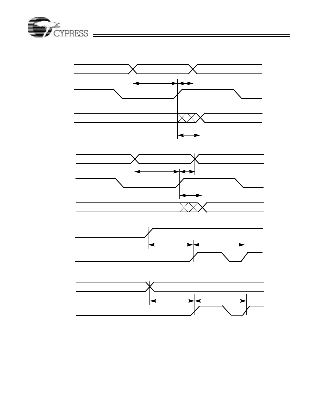
Delta39K™ ISR
™
ly
Switching Waveforms (continued)
Registered Output with Synchronous Clocking (Macrocell)
INPUT
SYNCHRONOUS
CLOCK
REGISTERED
OUTPUT
Registered Input in I/O Cell
DATA
INPUT
t
MCS
t
IOS
t
MCH
t
MCCO
t
IOH
CPLD Fami
INPUT REGISTER
CLOCK
REGISTERED
OUTPUT
Clock to Clock
INPUT REGISTER
CLOCK
MACROCELL
REGISTER CLOCK
PT Clock to PT Clock
DATA
INPUT
PT CLOCK
t
ICS
t
MCSPT
t
IOCO
t
SCS
t
SCS2PT
Document #: 38-03039 Rev. *H Page 25 of 86
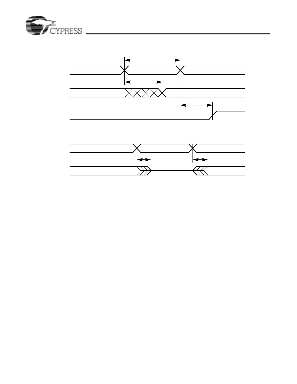
Delta39K™ ISR
™
ly
Switching Waveforms (continued)
Asynchronous Reset/Preset
RESET/PRESET
INPUT
REGISTERED
OUTPUT
CLOCK
Output Enable/Disable
GLOBAL CONTROL
INPUT
t
PRO
t
PRW
CPLD Fami
t
PRR
t
ER
t
EA
OUTPUTS
Document #: 38-03039 Rev. *H Page 26 of 86

Delta39K™ ISR
™
ly
Switching Waveforms (continued)
Cluster Memory Asynchronous Timing
ADDRESS (AT
THE CLUSTER
INPUT)
WRITE ENAB LE
INPUT
t
CLMCLAA
OUTPUT
READ
t
CLMPWE
CPLD Fami
READWRITE
t
CLMCLAA
Cluster Memory Asynchronous Timing 2
ADDRESS (A T THE
I/O PIN)
WRITE ENABLE
INPUT
t
CLMAA
OUTPUT
READ
t
CLMSA
t
CLMPWE
t
CLMSD
t
CLMHA
t
CLMHD
READWRITE
t
CLMAA
Document #: 38-03039 Rev. *H Page 27 of 86

Delta39K™ ISR
™
ly
Switching Waveforms (continued)
Cluster Memory Synchronous Flow-Through Timing
GLOBAL
CLOCK
ADDRESS
WRITE
ENABLE
REGISTERED
INPUT
t
CLMS
t
CLMH
t
CLMDV1
READ
t
CLMS
t
CLMH
t
CLMDV1
WRITE
t
CLMCYC1
CPLD Fami
READ
t
CLMS
t
CLMH
t
CLMDV1
REGISTERED
OUTPUT
Cluster Memory Internal Clocki ng
MACROCELL
INPUT CLOCK
CLUSTER MEMORY
INPUT CLOCK
CLUSTER MEMORY
OUTPUT CLOCK
t
CLMMACS1
t
CLMMACS2
t
MACCLMS1
t
MACCLMS2
Document #: 38-03039 Rev. *H Page 28 of 86

Delta39K™ ISR
™
ly
Switching Waveforms (continued)
Cluster Memory Output Register Timing (Asynchronous Inputs)
ADDRESS
WRITE
ENABLE
INPUT
GLOBAL CLOCK
(OUTPUT REGISTER)
t
CLMCYC2
t
CLMDV2
CPLD Fami
EGISTERED
UTPUT
Cluster Memory Output Register Timing (Synchronous Inputs)
ADDRESS
WRITE
ENABLE
INPUT
t
CLMCYC2
GLOBAL CLOCK
(INPUT REGISTER)
t
CLMS
GLOBAL CLOCK
(OUTPUT REGISTER)
t
CLMDV2
t
CLMH
REGISTERED
OUTPUT
Document #: 38-03039 Rev. *H Page 29 of 86

Delta39K™ ISR
™
ly
Channel Memory DP Asynchronous Timing
Switching Waveforms (continued)
ADDRESS
WRITE
ENABLE
DATA
INPUT
A
n-1
t
CHMSA
t
CHMPWE
t
CHMSD
A
n
t
CHMHA
t
CHMHD
D
n
t
CHMAA
A
n+1
CPLD Fami
A
n+2
t
CHMAA
OUTPUT
D
n–1
Channel Memory Internal Clocking
MACROCELL INPUT
CLOCK
CHANNEL MEMORY
INPUT CLOCK
CHANNEL MEMORY
OUTPUT CLOCK
t
CHMMACS1
t
CHMMACS2
D
n
t
MACCHMS1
t
MACCHMS2
D
n+1
Document #: 38-03039 Rev. *H Page 30 of 86

Delta39K™ ISR
™
ly
Switching Waveforms (continued)
Channel Memory Internal Clocking 2
MACROCELL INPUT
CLOCK
t
CHMMACS
FIFO READ
CLOCK
FIFO WRITE
CLOCK
FIFO READ OR
WRITE CLOCK
Channel Memory DP SRAM Flow-Through R/W Timing
t
MACCHMS
t
CHMMACF
CPLD Fami
CLOCK
ADDRESS
WRITE
ENABLE
DATA
INPUT
OUTPUT
t
t
CHMS
A
n–1
D
n–1
D
n–1
t
CHMH
A
n
t
CHMDV1
CHMCYC1
D
t
CHMS
n
D
A
n+1
t
CHMH
n+1
t
CHMDV1
A
n+2
t
CHMDV1
D
n+1
D
n+2
t
CHMDV1
A
n+3
D
n+3
D
n+3
Document #: 38-03039 Rev. *H Page 31 of 86

Delta39K™ ISR
™
ly
Switching Waveforms (continued)
Channel Memory DP SRAM Pipeline R/W Timing
CLOCK
ADDRESS
WRITE
ENABLE
A
t
n–1
CHMS
t
CHMS
A
t
CHMH
t
CHMH
n
t
CHMCYC2
t
CHMS
A
n+1
t
CHMH
CPLD Fami
A
n+2
A
n+3
DATA
INPUT
OUTPUT
D
n–1
D
n–1
Dual-Port Asynchronous Address Match Busy Signal
ADDRESS A
ADDRESS B
ADDRESS
MATCH
B
n
A
n–1
t
CHMBA
A
n
A
n
D
n+1
t
CHMDV2
D
n+3
t
CHMDV2
D
n
t
CHMDV2
D
n+1
t
CHMBA
D
n+2
A
n+1
Document #: 38-03039 Rev. *H Page 32 of 86

Delta39K™ ISR
™
ly
Switching Waveforms (continued)
Dual-Port Synchronous Address Match Busy Signal
CLOCK
ADDRESS A
ADDRESS B
ADDRESS
MATCH
A
B
n–1
n–1
t
CHMS
t
CHMBDV
A
n
A
n
t
CHMS
CPLD Fami
B
n+1
t
CHMBDV
Document #: 38-03039 Rev. *H Page 33 of 86

Delta39K™ ISR
™
ly
Channel Memory Synchronous FIFO Empty/Write Timing
Switching Waveforms (continued)
PORT B CLOCK
WRITE ENAB LE
REGISTERED
INPUT
EMPTY FLAG
(Active LOW)
t
CHMFS
t
CHMCLK
t
CHMFH
D
n+1
CPLD Fami
PORT A CLOCK
READ ENABLE
RE
REGISTERED
OUTPUT
t
CHMSKEW2
t
CHMFO
t
CHMFO
t
CHMFRDV
Document #: 38-03039 Rev. *H Page 34 of 86

Delta39K™ ISR
™
ly
Switching Waveforms (continued)
Channel Memory Synchronous FIFO Full/Read Timing
PORT A CLOCK
READ ENABLE
REGISTERED
OUTPUT
t
CHMFS
t
CHMFH
t
CHMFRDV
t
CHMCLK
CPLD Fami
FULL FLAG
(Active LOW)
PORT B CLOCK
WRITE ENABLE
REGISTERED
INPUT
t
CHMSKEW1tCHMFO
t
CHMS
t
CHMFO
t
CHMH
Document #: 38-03039 Rev. *H Page 35 of 86

Delta39K™ ISR
™
ly
Switching Waveforms (continued)
Channel Memory Synchronous FIFO Programmable Flag Timing
PORT B CLOCK
t
CHMFH
t
CHMSKEW3
WRITE ENABLE
PROGRAMMABLE
ALMOST EMPTY FLAG
(active LOW)
PORT A CLOCK
t
CHMFS
t
CHMFO
t
CHMCLK
t
CHMFS
CPLD Fami
t
CHMFO
t
CHMFH
READ ENABLE
PORT B CLOCK
WRITE ENABLE
PROGRAMMABLE
ALMOST FULL FLAG
(Active LOW)
PORT A CLOCK
t
CHMFO
t
CHMCLK
t
CHMSKEW3
t
CHMFO
READ ENABLE
Document #: 38-03039 Rev. *H Page 36 of 86

Delta39K™ ISR
™
ly
Channel Memory Synchronous FIFO Master Reset Timing
P
2
2
3
4
6
C
F
3
G
3
5
1
O
V
Z
Switching Waveforms (continued)
t
MASTER
RESET INPUT
READ ENABLE /
WRITE ENABLE
EMPTY/FULL
PROGRAMMABLE
ALMOST EMPTY
FLAGS
HALF-FULL/
PROGRAMMABLE
ALMOST FULL
FLAGS
CHMFRS
t
CHMFRSF
t
CHMFRSF
t
CHMFRSF
t
CHMFRSR
CPLD Fami
REGISTERED
OUTPUT
C Y 3 9 1 0 0 V 6 7 6 - 2 0 0 M B C
ypress Semiconductor ID
amily Type
9 = Delta39K Family
ate Density
0=30k Usable Gates 165 = 165k Usable Gates
0=50k Usable Gates 200 = 200k Usable Gates
00=100k Usable Gates
perating Reference Voltage
= 3.3V or 2.5V Supply Voltage
= 1.8V Supply Voltage
in Count
08 = 208 Leads
56 = 256 Balls
88 = 388 Balls
84 = 484 Balls
76 = 676 Balls
Operating Conditions
Commercial 0°C to +70°C
Industrial --40°C to +85°C
Package Type
N = Plastic Quad Flat Pac k (PQFP)
NT = Thermally Enhanced Quad Flat Pack (EQFP)
BG = Ball Grid Array (BGA)
BB = Fine-pitch Ball Grid Array (FBGA)
1.0-mm Lead Pitch
MG = Self-Boot Solution -- Ball Grid Array
MB = Self-Boot Solution -- Fine Pitch Ball Grid Array
1.0-mm Lead Pitch
Speed
233 = 233 MHz 125 = 125 MHz
200 = 200 MHz 83 = 83 MHz
181 = 181 MHz
Document #: 38-03039 Rev. *H Page 37 of 86

Delta39K™ ISR
™
ly
CPLD Fami
Delta39K Part Numbers (Ordering Information)
Device
39K30 233 CY39030V208-233NTC NT208 208-Lead Enhanced Quad Flat Pack Commercial
39K50 233 CY39050V208-233NTC NT208 208-Lead Enhanced Quad Flat Pack Commercial
39K50 125 CY39050V208-125NTI NT208 208-Lead Enhanced Quad Flat Pack Industrial
39K100 200 CY39100V208B-200NTC NT208 208-Lead Enhanced Quad Flat Pack Commercial
Speed
(MHz) Ordering Code
CY39030V256-233BBC BB256 256-Lead Fine Pitch Ball Grid Array
CY39030V256-233MBC MB256 256-Lead Fine Pitch Ball Grid Array ÷
125 CY39030V208-125NTC NT208 208-Lead Enhanced Quad Flat Pack
CY39030V256-125BBC BB256 256-Lead Fine Pitch Ball Grid Array
CY39030V256-125MBC MB256 256-Lead Fine Pitch Ball Grid Array ÷
CY39030V208-125NTI NT208 208-Lead Enhanced Quad Flat Pack Industrial
CY39030V256-125BBI BB256 256-Lead Fine Pitch Ball Grid Array
83 CY39030V208-83NTC NT208 208-Lead Enhanced Quad Flat Pack Commercial
CY39030V256-83BBC BB256 256-Lead Fine Pitch Ball Grid Array
CY39030V256-83MBC MB256 256-Lead Fine Pitch Ball Grid Array ÷
CY39030V208-83NTI NT208 208-Lead Plastic Quad Flat Pack Industrial
CY39030V256-83BBI BB256 256-Lead Fine Pitch Ball Grid Array
CY39050V256-233BBC BB256 256-Lead Fine Pitch Ball Grid Array
CY39050V388-233MGC MG388 388-Lead Ball Grid Array ÷
CY39050V484-233MBC MB484 484-Lead Fine Pitch Ball Grid Array ÷
125 CY39050V208-125NTC NT208 208-Lead Enhanced Quad Flat Pack
CY39050V256-125BBC BB256 256-Lead Fine Pitch Ball Grid Array
CY39050V388-125MGC MG388 388-Lead Pitch Ball Grid Array ÷
CY39050V484-125MBC MB484 484-Lead Fine Pitch Ball Grid Array ÷
CY39050V256-125BBI BB256 256-Lead Fine Pitch Ball Grid Array
83 CY39050V208-83NTC NT208 208-Lead Enhanced Quad Flat Pack Commercial
CY39050V256-83BBC BB256 256-Lead Fine Pitch Ball Grid Array
CY39050V388-83MGC MG388 388-Lead Ball Grid Array ÷
CY39050V484-83MBC MB484 484-Lead Fine Pitch Ball Grid Array ÷
CY39050V208-83NTI NT208 208-Lead Plastic Quad Flat Pack Industrial
CY39050V256-83BBI BB256 256-Lead Fine Pitch Ball Grid Array
CY39100V256B-200BBC BB256 256-Lead Fine Pitch Ball Grid Array
CY39100V484B-200BBC BB484 484-Lead Fine Pitch Ball Grid Array
CY39100V388B-200MGC MG388 388-Lead Ball Grid Array ÷
CY39100V676B-200MBC MB676 676-Lead Fine Pitch Ball Grid Array ÷
Package
Name Package Type
Self-Boot
Solution
Operating
Range
Document #: 38-03039 Rev. *H Page 38 of 86

Delta39K™ ISR
™
ly
CPLD Fami
Delta39K Part Numbers (Ordering Information) (continued)
Device
39K100 125 CY39100V208B-125NTC NT208 208-Lead Enhanced Quad Flat Pack Commercial
39K165 181 CY39165V208-181NTC NT208 208-Lead Enhanced Quad Flat Pack Commercial
Speed
(MHz) Ordering Code
CY39100V256B-125BBC BB256 256-Lead Fine Pitch Ball Grid Array
CY39100V484B-125BBC BB484 484-Lead Fine Pitch Ball Grid Array
CY39100V388B-125MGC MG388 388-Lead Ball Grid Array ÷
CY39100V676B-125MBC MB676 676-Lead Fine Pitch Ball Grid Array ÷
CY39100V208B-125NTI NT208 208-Lead Enhanced Quad Flat Pack Industrial
CY39100V256B-125BBI BB256 256-Lead Fine Pitch Ball Grid Array
CY39100V484B-125BBI BB484 484-Lead Fine Pitch Ball Grid Array
83 CY39100V208B-83NTC NT208 208-Lead Enhanced Quad Flat Pack Commercial
CY39100V256B-83BBC BB256 256-Lead Fine Pitch Ball Grid Array
CY39100V484B-83BBC BB484 484-Lead Fine Pitch Ball Grid Array
CY39100V388B-83MGC MG388 388-Lead Ball Grid Array ÷
CY39100V676B-83MBC MB676 676-Lead Fine Pitch Ball Grid Array ÷
CY39100V208B-83NTI NT208 208-Lead Enhanced Quad Flat Pack Industrial
CY39100V256B-83BBI BB256 256-Lead Fine Pitch Ball Grid Array
CY39100V484B-83BBI BB484 484-Lead Fine Pitch Ball Grid Array
CY39165V484-181BBC BB484 484-Lead Fine Pitch Ball Grid Array
CY39165V388-181MGC MG388 388-Lead Ball Grid Array ÷
CY39165V676-181MBC MB676 676-Lead Fine Pitch Ball Grid Array ÷
125 CY39165V208-125NTC NT208 208-Lead Enhanced Quad Flat Pack Commercial
CY39165V484-125BBC BB484 484-Lead Fine Pitch Ball Grid Array
CY39165V388-125MGC MG388 388-Lead Ball Grid Array ÷
CY39165V676-125MBC MB676 676-Lead Fine Pitch Ball Grid Array ÷
CY39165V208-125NTI NT208 208-Lead Enhanced Quad Flat Pack Industrial
CY39165V484-125BBI BB484 484-Lead Fine Pitch Ball Grid Array
83 CY39165V208-83NTC NT208 208-Lead Enhanced Quad Flat Pack Commercial
CY39165V484-83BBC BB484 484-Lead Fine Pitch Ball Grid Array
CY39165V388-83MGC MG388 388-Lead Ball Grid Array ÷
CY39165V676-83MBC MB676 676-Lead Fine Pitch Ball Grid Array ÷
CY39165V208-83NTI NT208 208-Lead Enhanced Quad Flat Pack Industrial
CY39165V484-83BBI BB484 484-Lead Fine Pitch Ball Grid Array
Package
Name Package Type
Self-Boot
Solution
Operating
Range
Document #: 38-03039 Rev. *H Page 39 of 86

Delta39K™ ISR
™
ly
CPLD Fami
Delta39K Part Numbers (Ordering Information) (continued)
Device
39K200 181 CY39200V208-181NTC NT208 208-Lead Enhanced Quad Flat Pack Commercial
CPLD Boot EEPROM
Speed
(MHz) Ordering Code
CY39200V484-181BBC BB484 484-Lead Fine Pitch Ball Grid Array
CY39200V388-181MGC MG388 388-Lead Ball Grid Array ÷
CY39200V676-181MBC MB676 676-Lead Fine Pitch Ball Grid Array ÷
125 CY39200V208-125NTC NT208 208-Lead Enhanced Quad Flat Pack Commercial
CY39200V484-125BBC BB484 484-Lead Fine Pitch Ball Grid Array
CY39200V388-125MGC MG388 388-Lead Ball Grid Array ÷
CY39200V676-125MBC MB676 676-Lead Fine Pitch Ball Grid Array ÷
CY39200V208-125NTI NT208 208-Lead Enhanced Quad Flat Pack Industrial
CY39200V484-125BBI BB484 484-Lead Fine Pitch Ball Grid Array
83 CY39200V208-83NTC NT208 208-Lead Enhanced Quad Flat Pack Commercial
CY39200V484-83BBC BB484 484-Lead Fine Pitch Ball Grid Array
CY39200V388-83MGC MG388 388-Lead Ball Grid Array ÷
CY39200V676-83MBC MB676 676-Lead Fine Pitch Ball Grid Array ÷
CY39200V208-83NTI NT208 208-Lead Enhanced Quad Flat Pack Industrial
CY39200V484-83BBI BB484 484-Lead Fine Pitch Ball Grid Array
[17]
Part Numbers (Ordering Information)
Device
2 Mbit 15 A T17LV002-10JC 20J 20-Lead Plastic Leaded Chip Carrier Commercial
1 Mbit 15 A T17LV010-10JC 20J 20-Lead Plastic Leaded Chip Carrier Commercial
512 Kbit 15 AT17L V5 12-10JC 20J 20-Lead Plastic Leaded Chip Carri er Commercial
Speed
(MHz) Ordering Code
10 AT17L V0 02-10JC 20J 20-Lead Plastic Leaded Chip Carri er Industrial
10 AT17L V0 10-10JI 20J 20-Lead Plastic Leaded Chi p Carrier Industrial
10 AT17L V5 12-10JI 20J 20-Lead Plastic Leaded Chi p Carrier Industrial
Package
Name Package Type
Package
Name Package Type
Self-Boot
Solution
Operating
Range
Operating
Range
Recommended ATMEL CPLD Boot EEPROM for corresponding Delta39K CPLDs
CPLD Device Recommended boot EEPROM
39K30 AT17LV512
39K50 AT17LV512
39K100 AT17LV010
39K165 AT17LV002
39K200 AT17LV002
Note:
17. Refer to the data sheets at www.atmel.com for detailed architectural and timing information.
Document #: 38-03039 Rev. *H Page 40 of 86

Delta39K™ ISR
™
ly
Package Diagrams
208-Lead Enhanced Quad Flat Pack (EQFP) NT208
CPLD Fami
51-85069-*B
Document #: 38-03039 Rev. *H Page 41 of 86

Delta39K™ ISR
™
ly
388-Lead Ball Grid Array MG388
Package Diagrams (continued)
CPLD Fami
51-85103-*C
Document #: 38-03039 Rev. *H Page 42 of 86

Delta39K™ ISR
™
ly
Package Diagrams (continued)
TOP VIEW
PIN 1 CORNER
A
B
C
D
E
F
G
H
J
K
L
M
N
P
R
T
0.25 C
0.70±0.05
A1
SEATING PLANE
C
A1 0.36 0.56
A 1.40 MAX. 1.60 MAX.
256-Ball FBGA (17 x 17 mm) BB256
Ø0.05MC
Ø0.25MCAB
Ø0.45±0.05(256X)-CPLD DEVICES (37K & 39K)
161513 141210 11928765431
0.15 C
A
-0.05
+0.10
0.35
Ø0.50±0.05(256X)-ALL OTHER DEVICES
1.00
15.00
17.00±0.10
7.50
B
A
0.20(4X)
BOTTOM VIEW
16 15 14 13 12 11
7.50
REFERENCE JEDEC MO-192
CPLD Fami
PIN 1 CORNER
1098765432 1
1.00
15.00
17.00±0.10
51-85108-*D
A
B
C
D
E
F
G
H
J
K
L
M
N
P
R
T
Document #: 38-03039 Rev. *H Page 43 of 86

Delta39K™ ISR
™
ly
Package Diagrams (continued)
TOP VIEW
A1 CORNER
957864231
A
B
C
D
E
F
G
H
J
K
L
M
N
P
R
T
U
V
W
Y
AA
AB
484-ball FBGA (23 mm x 23 mm x 1.6 mm) BB484
15 19202117
131011
22
181612 14
21.00
23.00±0.10
A
2120191817161514131211
22
1.00
10.50
BOTTOM VIEW
Ø0.05 M C
Ø0.25MCAB
Ø0.60±0.10(484X)
10.50
CPLD Fami
A1 CORNER
10987654321
1.00
21.00
A
B
C
D
E
F
G
H
J
K
L
M
N
P
R
T
U
V
W
Y
AA
AB
0.25 C
0.70±0.05
0.56
0.20 C
C
SEATING PLANE
1.90 MAX
0.50±0.10
B
0.10(4X)
23.00±0.10
51-85124-*D
Document #: 38-03039 Rev. *H Page 44 of 86

Delta39K™ ISR
™
ly
Package Diagrams
(continued)
676-Ball FBGA (27 x 27 x 1.6 mm) BB676/MB676
CPLD Fami
Pin Tables
Table 8. Pin Definition Table
Pin Name Function Description
GCLK0-3 Input Global Clock signals 0 through 3
GCTL0-3 Input Global Control signals 0 through 3
GND Ground Ground
IO/V
REF0
IO/V
REF1
IO/V
REF2
IO/V
REF3
IO/V
REF4
IO/V
REF5
IO/V
REF6
IO/V
REF7
IO Input/Output Input or Output pin
IO6/Lock Input/Output Dual function pin: IO in Bank 6 or PLL lock output signal
MSEL Input Mode Select Pin (see Table 9)
Input/Output Dual function pin: IO or Reference Voltage for Bank 0
Input/Output Dual function pin: IO or Reference Voltage for Bank 1
Input/Output Dual function pin: IO or Reference Voltage for Bank 2
Input/Output Dual function pin: IO or Reference Voltage for Bank 3
Input/Output Dual function pin: IO or Reference Voltage for Bank 4
Input/Output Dual function pin: IO or Reference Voltage for Bank 5
Input/Output Dual function pin: IO or Reference Voltage for Bank 6
Input/Output Dual function pin: IO or Reference Voltage for Bank 7
51-85125-*B
Document #: 38-03039 Rev. *H Page 45 of 86

Delta39K™ ISR
™
ly
Table 8. Pin Definition Table
Pin Name Function Description
Reconfig Input Pin to start configuration of Delta39K
TCLK Input JTAG Test Clock
TDI Input JTAG T est Data In
TDO Output JTAG Test Data Out
TMS Input JTAG Test Mode Select
V
CC
V
CCIO0
V
CCIO1
V
CCIO2
V
CCIO3
V
CCIO4
V
CCIO5
V
CCIO6
V
CCIO7
V
CCJTAG
V
CCCNFG
[18]
V
CCPLL
V
CCPRG
Config_Done Output Flag indicating that configuration is complete
CCLK Output Configuration Clock for serial interface with the external boot PROM
CCE Output Chip select for the external boot PROM (active low)
Data Input Pin to receive configuration data from the external boot PROM
Reset Output Reset signal to interface with the external boot PROM
Table 9. Mode Select (MSEL) Pin Connectivity Table
GND Delta39K - Self-Boot™ Solution
V
CCCNFG
Power Operating Voltage
Power VCC for I/O bank 0
Power VCC for I/O bank 1
Power VCC for I/O bank 2
Power VCC for I/O bank 3
Power VCC for I/O bank 4
Power VCC for I/O bank 5
Power VCC for I/O bank 6
Power VCC for I/O bank 7
Power VCC for JTAG pins
Power VCC for Configuration port
Power VCC for PLL
Power VCC for programming the Self-Boot™ solution embedded boot PROM
Table 10. I/O Banks for Global Clock and Global Control
Pins (in all densities and packages)
Delta39K - with external boot PROM
Bank
GCLK[0]
GCTL[0]
0567
Number
GCLK[1]
GCTL[1]
CPLD Fami
GCLK[2]
GCTL[2]
GCLK[3]
GCTL[3]
Table 11. 208 EQFP/PQFP Pin Table
Pin CY39030 CY39050 CY39100 CY39165 CY39200
1 GCTL0 GCTL0 GCTL0 GCTL0 GCTL0
2 GND GND GND GND GND
3 GCLK0 GCLK0 GCLK0 GCLK0 GCLK0
4 GND GND GND GND GND
5 IO0 IO0 IO0 IO0 IO0
6 IO0 IO0 IO0 IO0 IO0
7 IO0 IO0 IO0 IO0 IO0
8IO/V
REF0
IO/V
REF0
IO/V
REF0
IO/V
REF0
IO/V
REF0
9 IO0 IO0 IO0 IO0 IO0
10 IO0 IO0 IO0 IO0 IO0
11 V
Note:
18. The PLL is available in Delta39K ‘V’ devices (2.5V/3.3V) and not in Delta39K ‘Z’ devices (1.8V). In Delta39K ‘Z’ devices, connect V
CCIO0
Document #: 38-03039 Rev. *H Page 46 of 86
V
CCIO0
V
CCIO0
V
CCIO0
CCPLL
V
CCIO0
to VCC.

Delta39K™ ISR
™
ly
Table 11. 208 EQFP/PQFP Pin Table (continued)
Pin CY39030 CY39050 CY39100 CY39165 CY39200
12 IO0 IO0 IO0 IO0 IO0
13 IO0 IO0 IO0 IO0 IO0
14 IO0 IO0 IO0 IO0 IO0
15 IO0 IO0 IO0 IO0 IO0
16 IO/V
REF0
IO/V
17 IO0 IO0 IO0 IO0 IO0
18 IO0 IO0 IO0 IO0 IO0
19 IO0 IO0 IO0 IO0 IO0
20 V
[19]
21
[19]
22
23 V
CCIO0
IO0 IO0 IO0 IO0 IO0
IO0 IO0 IO0 IO0 IO0
CC
24 GND GND GND GND GND
25 NC NC V
26 NC NC GND GND GND
[19]
27
28 V
29 V
[19]
30
[19]
31
[19]
32
IO/V
IO/V
REF0
CCIO0
CCIO1
REF1
IO/V
IO/V
IO1 IO1 IO1 IO1 IO1
IO1 IO1 IO1 IO1 IO1
33 IO1 IO1 IO1 IO1 IO1
34 IO1 IO1 IO1 IO1 IO1
35 V
CCIO1
36 GND GND GND GND GND
37 IO1 IO1 IO1 IO1 IO1
38 IO1 IO1 IO1 IO1 IO1
39 IO1 IO1 IO1 IO1 IO1
40 IO/V
REF1
IO/V
41 IO1 IO1 IO1 IO1 IO1
42 IO1 IO1 IO1 IO1 IO1
43 IO1 IO1 IO1 IO1 IO1
44 IO1 IO1 IO1 IO1 IO1
45 V
46 V
CCPRG
CCIO1
V
47 GND GND GND GND GND
48 IO1 IO1 IO1 IO1 IO1
49 IO/V
REF1
IO/V
50 IO1 IO1 IO1 IO1 IO1
51 IO1 IO1 IO1 IO1 IO1
52 V
CCCNFG
V
53 Data Data Data Data Data
54 Config_Done Config_Done Config_Done Config_Done Config_Done
55 Reset Reset Reset Reset Reset
REF0
V
CCIO0
V
CC
REF0
V
CCIO0
V
CCIO1
REF1
V
CCIO1
REF1
CCPRG
V
CCIO1
REF1
CCCNFG
IO/V
V
CCIO0
V
IO/V
V
CCIO0
V
CCIO1
IO/V
V
CCIO1
IO/V
V
CCPRG
V
CCIO1
IO/V
V
CCCNFG
REF0
CC
CC
REF0
REF1
REF1
REF1
IO/V
V
CCIO0
V
V
IO/V
V
CCIO0
V
CCIO1
IO/V
V
CCIO1
IO/V
V
CCPRG
V
CCIO1
IO/V
V
CCCNFG
CPLD Fami
REF0
CC
CC
REF0
REF1
REF1
REF1
IO/V
V
CCIO0
V
CC
V
CC
IO/V
V
CCIO0
V
CCIO1
IO/V
V
CCIO1
IO/V
V
CCPRG
V
CCIO1
IO/V
V
CCCNFG
REF0
REF0
REF1
REF1
REF1
Document #: 38-03039 Rev. *H Page 47 of 86

Delta39K™ ISR
™
ly
Table 11. 208 EQFP/PQFP Pin Table (continued)
Pin CY39030 CY39050 CY39100 CY39165 CY39200
56 Reconfig Reconfig Reconfig Reconfig Reconfig
57 CCE CCE CCE CCE CCE
58 CCLK CCLK CCLK CCLK CCLK
59 V
CCCNFG
V
60 MSEL MSEL MSEL MSEL MSEL
61 IO2 IO2 IO2 IO2 IO2
62 IO2 IO2 IO2 IO2 IO2
63 IO2 IO2 IO2 IO2 IO2
64 IO/V
REF2
IO/V
65 IO2 IO2 IO2 IO2 IO2
66 V
CCIO2
67 GND GND GND GND GND
68 IO2 IO2 IO2 IO2 IO2
69 IO2 IO2 IO2 IO2 IO2
70 IO2 IO2 IO2 IO2 IO2
71 IO2 IO2 IO2 IO2 IO2
72 IO/V
REF2
IO/V
73 GND GND GND GND GND
74 V
75 V
CCIO2
CC
76 GND GND GND GND GND
77 NC NC V
78 NC NC GND GND GND
79 IO2 IO2 IO2 IO2 IO2
80 IO/V
[19]
81
[19]
82
[19]
83
84 V
85 V
[19]
86
[19]
87
[19]
88
89 V
REF2
IO2 IO2 IO2 IO2 IO2
IO2 IO2 IO2 IO2 IO2
IO2 IO2 IO2 IO2 IO2
CCIO2
CCIO3
IO3 IO3 IO3 IO3 IO3
IO3 IO3 IO3 IO3 IO3
IO/V
REF3
CCIO3
IO/V
IO/V
90 GND GND GND GND GND
91 IO3 IO3 IO3 IO3 IO3
92 IO3 IO3 IO3 IO3 IO3
93 IO3 IO3 IO3 IO3 IO3
94 IO3 IO3 IO3 IO3 IO3
95 IO3 IO3 IO3 IO3 IO3
96 IO/V
REF3
IO/V
97 IO3 IO3 IO3 IO3 IO3
98 V
CCIO3
99 IO3 IO3 IO3 IO3 IO3
CCCNFG
REF2
V
CCIO2
REF2
V
CCIO2
V
CC
REF2
V
CCIO2
V
CCIO3
REF3
V
CCIO3
REF3
V
CCIO3
V
CCCNFG
IO/V
V
CCIO2
IO/V
V
CCIO2
V
IO/V
V
CCIO2
V
CCIO3
IO/V
V
CCIO3
IO/V
V
CCIO3
REF2
REF2
CC
CC
REF2
REF3
REF3
V
CCCNFG
IO/V
V
CCIO2
IO/
VREF2
V
CCIO2
V
V
IO/V
V
CCIO2
V
CCIO3
IO/V
V
CCIO3
IO/V
V
CCIO3
CPLD Fami
REF2
CC
CC
REF2
REF3
REF3
V
CCCNFG
IO/V
V
CCIO2
IO/V
V
CCIO2
V
CC
V
CC
IO/V
V
CCIO2
V
CCIO3
IO/V
V
CCIO3
IO/V
V
CCIO3
REF2
REF2
REF2
REF3
REF3
Document #: 38-03039 Rev. *H Page 48 of 86

Delta39K™ ISR
™
ly
Table 11. 208 EQFP/PQFP Pin Table (continued)
Pin CY39030 CY39050 CY39100 CY39165 CY39200
100 GND GND GND GND GND
101 IO3 IO3 IO3 IO3 IO3
102 IO3 IO3 IO3 IO3 IO3
103 IO3 IO3 IO3 IO3 IO3
104 IO/V
REF3
IO/V
105 IO4 IO4 IO4 IO4 IO4
106 IO4 IO4 IO4 IO4 IO4
107 IO4 IO4 IO4 IO4 IO4
108 IO/V
REF4
IO/V
109 IO4 IO4 IO4 IO4 IO4
110 IO4 IO4 IO4 IO4 IO4
111 V
CCIO4
112 GND GND GND GND GND
113 IO4 IO4 IO4 IO4 IO4
114 V
CCPRG
V
115 IO4 IO4 IO4 IO4 IO4
116 IO/V
REF4
IO/V
117 IO4 IO4 IO4 IO4 IO4
118 IO4 IO4 IO4 IO4 IO4
119 IO4 IO4 IO4 IO4 IO4
120 IO4 IO4 IO4 IO4 IO4
121 IO4 IO4 IO4 IO4 IO4
[19]
122
[19]
123
124 V
IO/V
REF4
IO/V
IO4 IO4 IO4 IO4 IO4
CCIO4
125 GND GND GND GND GND
[19]
126
127 V
IO4 IO4 IO4 IO4 IO4
CC
128 GND GND GND GND GND
129 NC NC V
130 NC NC GND GND GND
131 V
132 V
[19]
133
[19]
134
[19]
135
CCIO4
CCIO5
IO5 IO5 IO5 IO5 IO5
IO5 IO5 IO5 IO5 IO5
IO/V
REF5
IO/V
136 IO5 IO5 IO5 IO5 IO5
137 IO5 IO5 IO5 IO5 IO5
138 V
CCIO5
139 IO5 IO5 IO5 IO5 IO5
140 IO5 IO5 IO5 IO5 IO5
141 IO5 IO5 IO5 IO5 IO5
142 IO/V
REF5
IO/V
143 IO5 IO5 IO5 IO5 IO5
V
CCIO4
CCPRG
V
CCIO4
V
CC
V
CCIO4
V
CCIO5
V
CCIO5
REF3
REF4
REF4
REF4
REF5
REF5
IO/V
IO/V
V
V
CCPRG
IO/V
IO/V
V
V
V
IO/V
V
IO/V
REF3
REF4
CCIO4
REF4
REF4
CCIO4
V
CC
CC
CCIO4
CCIO5
REF5
CCIO5
REF5
IO/V
IO/V
V
CCIO4
V
CCPRG
IO/V
IO/V
V
CCIO4
V
V
V
CCIO4
V
CCIO5
IO/V
V
CCIO5
IO/V
CPLD Fami
REF3
REF4
REF4
REF4
CC
CC
REF5
REF5
IO/V
IO/V
V
V
CCPRG
IO/V
IO/V
V
V
V
IO/V
V
IO/V
REF3
REF4
CCIO4
REF4
REF4
CCIO4
V
CC
V
CC
CCIO4
CCIO5
REF5
CCIO5
REF5
Document #: 38-03039 Rev. *H Page 49 of 86
Delta39K™ ISR
™
ly
Table 11. 208 EQFP/PQFP Pin Table (continued)
Pin CY39030 CY39050 CY39100 CY39165 CY39200
144 IO5 IO5 IO5 IO5 IO5
145 IO5 IO5 IO5 IO5 IO5
146 IO5 IO5 IO5 IO5 IO5
147 IO5 IO5 IO5 IO5 IO5
148 V
149 IO/V
CCIO5
REF5
IO/V
150 IO5 IO5 IO5 IO5 IO5
151 IO5 IO5 IO5 IO5 IO5
152 GND GND GND GND GND
153 GCLK1 GCLK1 GCLK1 GCLK1 GCLK1
154 GND GND GND GND GND
155 GCTL1 GCTL1 GCTL1 GCTL1 GCTL1
156 TDO TDO TDO TDO TDO
157 TCLK TCLK TCLK TCLK TCLK
158 TDI TDI TDI TDI TDI
159 V
CCJTAG
V
160 GCLK2 GCLK2 GCLK2 GCLK2 GCLK2
161 GND GND GND GND GND
162 TMS TMS TMS TMS TMS
163 GCTL2 GCTL2 GCTL2 GCTL2 GCTL2
164 IO6 IO6 IO6 IO6 IO6
165 IO6 IO6 IO6 IO6 IO6
166 IO6 IO6 IO6 IO6 IO6
167 IO/V
REF6
IO/V
168 IO6 IO6 IO6 IO6 IO6
169 V
CCIO6
170 IO6 IO6 IO6 IO6 IO6
171 IO6 IO6 IO6 IO6 IO6
172 IO6 IO6 IO6 IO6 IO6
173 IO/V
REF6
IO/V
174 IO6 IO6 IO6 IO6 IO6
175 IO6 IO6 IO6 IO6 IO6
176 IO6 IO6 IO6 IO6 IO6
177 GND GND GND GND GND
178 V
179 V
CCIO6
CCPLL
180 GND GND GND GND GND
181 V
CC
182 GND GND GND GND GND
[19]
183
[19]
184
[19]
185
186 V
187 V
IO/V
REF6
IO/V
IO6 IO6 IO6 IO6 IO6
IO6/Lock IO6/Lock IO6/Lock IO6/Lock IO6/Lock
CCIO6
CCIO7
V
CCIO5
REF5
CCJTAG
REF6
V
CCIO6
REF6
V
CCIO6
V
CCPLL
V
CC
REF6
V
CCIO6
V
CCIO7
V
CCIO5
IO/V
V
CCJTAG
IO/V
V
CCIO6
IO/V
V
CCIO6
V
CCPLL
V
IO/V
V
CCIO6
V
CCIO7
REF5
REF6
REF6
CC
REF6
V
CCIO5
IO/V
V
CCJTAG
IO/V
V
CCIO6
IO/V
V
CCIO6
V
CCPLL
V
IO/V
V
CCIO6
V
CCIO7
CPLD Fami
REF5
REF6
REF6
CC
REF6
V
CCIO5
IO/V
V
CCJTAG
IO/V
V
CCIO6
IO/V
V
CCIO6
V
CCPLL
V
IO/V
V
CCIO6
V
CCIO7
REF5
REF6
REF6
CC
REF6
Document #: 38-03039 Rev. *H Page 50 of 86

Delta39K™ ISR
™
ly
Table 11. 208 EQFP/PQFP Pin Table (continued)
Pin CY39030 CY39050 CY39100 CY39165 CY39200
[19]
188
[19]
189
[19]
190
191 V
IO7 IO7 IO7 IO7 IO7
IO7 IO7 IO7 IO7 IO7
IO/V
REF7
CCIO7
IO/V
192 IO7 IO7 IO7 IO7 IO7
193 IO7 IO7 IO7 IO7 IO7
194 IO7 IO7 IO7 IO7 IO7
195 IO7 IO7 IO7 IO7 IO7
196 IO/V
REF7
IO/V
197 IO7 IO7 IO7 IO7 IO7
198 IO7 IO7 IO7 IO7 IO7
199 V
CCIO7
200 IO7 IO7 IO7 IO7 IO7
201 IO/V
REF7
IO/V
202 IO7 IO7 IO7 IO7 IO7
203 IO7 IO7 IO7 IO7 IO7
204 IO7 IO7 IO7 IO7 IO7
205 GND GND GND GND GND
206 GCLK3 GCLK3 GCLK3 GCLK3 GCLK3
207 GND GND GND GND GND
208 GCTL3 GCTL3 GCTL3 GCTL3 GCTL3
V
CCIO7
V
CCIO7
REF7
REF7
REF7
IO/V
V
IO/V
V
IO/V
REF7
CCIO7
REF7
CCIO7
REF7
IO/V
V
CCIO7
IO/V
V
CCIO7
IO/V
CPLD Fami
REF7
REF7
REF7
IO/V
V
IO/V
V
IO/V
REF7
CCIO7
REF7
CCIO7
REF7
Table 12. 388 BGA Pin Table
Pin CY39050 CY39100 CY39165 CY39200
A1 GND GND GND GND
A2 NC IO7 IO7 IO7
A3IO7IO7IO7IO7
A4IO7IO7IO7IO7
A5IO7IO7IO7IO7
A6IO7IO7IO7IO7
A7IO7IO7IO7IO7
A8 NC IO/VREF7 IO/VREF7 IO/VREF7
A9IO7IO7IO7IO7
A10 IO7 IO7 IO7 IO7
A11 IO/V
REF7
IO/V
REF7
IO/V
REF7
IO/V
REF7
A12 IO7 IO7 IO7 IO7
A13
A14
[19]
[19]
IO7IO7IO7IO7
IO6IO6IO6IO6
A15 IO6 IO6 IO6 IO6
A16 GND GND GND GND
A17 IO6 IO6 IO6 IO6
A18 IO6 IO6 IO6 IO6
Note:
19. Capacitance on these I/O pins meets the PCI spec (rev. 2.2), which requires IDSEL pin in a PCI design to have capacitance less than or equal to 8 pf. In the
document titled “Delta39K CPLD Family data sheet”, this spec is defined as C
All other I/O pins have a capacitance less than or equal to 10 pf.
PCI.
Document #: 38-03039 Rev. *H Page 51 of 86

Delta39K™ ISR
™
ly
CPLD Fami
Table 12. 388 BGA Pin Table (continued)
Pin CY39050 CY39100 CY39165 CY39200
A19 NC IO6 IO6 IO6
A20 NC IO6 IO6 IO6
A21 IO6 IO6 IO6 IO6
A22 IO/V
REF6
IO/V
REF6
IO/V
REF6
IO/V
REF6
A23 IO6 IO6 IO6 IO6
A24 IO6 IO6 IO6 IO6
A25 IO6 IO6 IO6 IO6
A26 GND GND GND GND
B1IO7IO7IO7IO7
B2 NC IO7 IO7 IO7
B3 NC IO7 IO7 IO7
B4 NC IO/V
REF7
IO/V
REF7
IO/V
REF7
B5IO7IO7IO7IO7
B6 IO/V
REF7
IO/V
REF7
IO/V
REF7
IO/V
REF7
B7IO7IO7IO7IO7
B8IO7IO7IO7IO7
B9IO7IO7IO7IO7
B10 IO/V
REF7
IO/V
REF7
IO/V
REF7
IO/V
REF7
B11 IO7 IO7 IO7 IO7
B12 IO7 IO7 IO7 IO7
B13
B14
[19]
[19]
IO7IO7IO7IO7
IO6IO6IO6IO6
B15 IO6 IO6 IO6 IO6
B16 IO6 IO6 IO6 IO6
B17 IO6/Lock IO6/Lock IO6/Lock IO6/Lock
B18 IO6 IO6 IO6 IO6
B19 IO6 IO6 IO6 IO6
B20 IO/VREF6 IO/VREF6 IO/VREF6 IO/VREF6
B21 IO6 IO6 IO6 IO6
B22 NC IO6 IO6 IO6
B23 NC IO6 IO6 IO6
B24 IO6 IO6 IO6 IO6
B25 IO6 IO6 IO6 IO6
B26 IO6 IO6 IO6 IO6
C1IO0IO0IO0IO0
C2 IO/V
REF7
IO/V
REF7
IO/V
REF7
IO/V
REF7
C3 NC IO7 IO7 IO7
C4IO7IO7IO7IO7
C5IO7IO7IO7IO7
C6 NC IO7 IO7 IO7
C7IO7IO7IO7IO7
C8IO7IO7IO7IO7
C9IO7IO7IO7IO7
C10 IO7 IO7 IO7 IO7
Document #: 38-03039 Rev. *H Page 52 of 86

Delta39K™ ISR
™
ly
CPLD Fami
Table 12. 388 BGA Pin Table (continued)
Pin CY39050 CY39100 CY39165 CY39200
C11 IO7 IO7 IO7 IO7
C12 IO7 IO7 IO7 IO7
[19]
C13
[19]
C14
C15 IO/V
IO7IO7IO7IO7
IO6IO6IO6IO6
REF6
IO/V
REF6
IO/V
REF6
IO/V
REF6
C16 IO6 IO6 IO6 IO6
C17 NC IO/V
REF6
IO/V
REF6
IO/V
REF6
C18 IO6 IO6 IO6 IO6
C19 IO6 IO6 IO6 IO6
C20 IO6 IO6 IO6 IO6
C21 IO6 IO6 IO6 IO6
C22 NC IO6 IO6 IO6
C23 NC IO6 IO6 IO6
C24 IO6 IO6 IO6 IO6
C25 IO/V
REF6
IO/V
REF6
IO/V
REF6
IO/V
REF6
C26 IO6 IO6 IO6 IO6
D1IO0IO0IO0IO0
D2IO0IO0IO0IO0
D3 IO/V
REF0
IO/V
REF0
IO/V
REF0
IO/V
REF0
D4IO7IO7IO7IO7
D5 GCTL3 GCTL3 GCTL3 GCTL3
D6 NC IO7 IO7 IO7
D7 GCLK3 GCLK3 GCLK3 GCLK3
D8 V
D9 V
D10 V
CCIO7
CCIO7
CCIO7
V
CCIO7
V
CCIO7
V
CCIO7
V
CCIO7
V
CCIO7
V
CCIO7
V
CCIO7
V
CCIO7
V
CCIO7
D11 IO7 IO7 IO7 IO7
D12 V
D13 V
D14 V
D15 V
CCIO7
CC
CCIO6
CCIO6
V
CCIO7
V
V
CCIO6
V
CCIO6
CC
V
CCIO7
V
V
CCIO6
V
CCIO6
CC
V
CCIO7
V
V
CCIO6
V
CCIO6
CC
D16 IO6 IO6 IO6 IO6
D17 V
D18 V
D19 V
CCPLL
CCIO6
CCIO6
V
CCPLL
V
CCIO6
V
CCIO6
V
CCPLL
V
CCIO6
V
CCIO6
V
CCPLL
V
CCIO6
V
CCIO6
D20 GCLK2 GCLK2 GCLK2 GCLK2
D21 NC IO/V
REF6
IO/V
REF6
IO/V
REF6
D22 GCTL2 GCTL2 GCTL2 GCTL2
D23 NC IO6 IO6 IO6
D24 IO5 IO5 IO5 IO5
D25 TMS TMS TMS TMS
D26 TCLK TCLK TCLK TCLK
E1IO0IO0IO0IO0
E2IO0IO0IO0IO0
Document #: 38-03039 Rev. *H Page 53 of 86

Delta39K™ ISR
™
ly
CPLD Fami
Table 12. 388 BGA Pin Table (continued)
Pin CY39050 CY39100 CY39165 CY39200
E3IO0IO0IO0IO0
E4 GCTL0 GCTL0 GCTL0 GCTL0
E23 GCLK1 GCLK1 GCLK1 GCLK1
E24 IO5 IO5 IO5 IO5
E25 TDI TDI TDI TDI
E26 TDO TDO TDO TDO
F1 NC IO0 IO0 IO0
F2 NC IO0 IO0 IO0
F3 NC IO0 IO0 IO0
F4IO0IO0IO0IO0
F23 NC IO5 IO5 IO5
F24 IO5 IO5 IO5 IO5
F25 IO5 IO5 IO5 IO5
F26 IO5 IO5 IO5 IO5
G1 IO0 IO0 IO0 IO0
G2 IO0 IO0 IO0 IO0
G3 IO/V
REF0
IO/V
REF0
IO/V
REF0
IO/V
REF0
G4 GCLK0 GCLK0 GCLK0 GCLK0
G23 GCTL1 GCTL1 GCTL1 GCTL1
G24 IO/V
REF5
IO/V
REF5
IO/V
REF5
IO/V
REF5
G25 IO5 IO5 IO5 IO5
G26 IO5 IO5 IO5 IO5
H1IO0IO0IO0IO0
H2 NC IO0 IO0 IO0
H3 NC IO0 IO0 IO0
H4 V
H23 V
CCIO0
CCJTAG
V
CCIO0
V
CCJTAG
V
CCIO0
V
CCJTAG
V
CCIO0
V
CCJTAG
H24 IO5 IO5 IO5 IO5
H25 IO5 IO5 IO5 IO5
H26 IO5 IO5 IO5 IO5
J1 NC IO0 IO0 IO0
J2 NC IO/V
REF0
IO/V
REF0
IO/V
REF0
J3 NC IO0 IO0 IO0
J4 V
J23 V
CCIO0
CCIO5
J24 NC IO/V
V
CCIO0
V
CCIO5
REF5
V
V
IO/V
CCIO0
CCIO5
REF5
V
V
IO/V
CCIO0
CCIO5
REF5
J25 IO5 IO5 IO5 IO5
J26 IO5 IO5 IO5 IO5
K1 NC IO0 IO0 IO0
K2 NC IO0 IO0 IO0
K3 NC IO0 IO0 IO0
K4 V
K23 V
CC
CCIO5
V
V
CCIO5
CC
V
V
CCIO5
CC
V
V
CCIO5
CC
K24 IO5 IO5 IO5 IO5
Document #: 38-03039 Rev. *H Page 54 of 86

Delta39K™ ISR
™
ly
CPLD Fami
Table 12. 388 BGA Pin Table (continued)
Pin CY39050 CY39100 CY39165 CY39200
K25 NC IO5 IO5 IO5
K26 NC IO5 IO5 IO5
L1IO0IO0IO0IO0
L2IO0IO0IO0IO0
L3IO0IO0IO0IO0
L4IO0IO0IO0IO0
L11 GND GND GND GND
L12 GND GND GND GND
L13 GND GND GND GND
L14 GND GND GND GND
L15 GND GND GND GND
L16 GND GND GND GND
L23 NC IO5 IO5 IO5
L24 IO/V
REF5
IO/V
REF5
IO/V
REF5
IO/V
REF5
L25 NC IO5 IO5 IO5
L26 NC IO5 IO5 IO5
M1IO0IO0IO0IO0
[19]
M2
[19]
M3
M4 V
IO0IO0IO0IO0
IO0IO0IO0IO0
CCIO0
V
CCIO0
V
CCIO0
V
CCIO0
M11 GND GND GND GND
M12 GND GND GND GND
M13 GND GND GND GND
M14 GND GND GND GND
M15 GND GND GND GND
M16 GND GND GND GND
M23 V
CCIO5
V
CCIO5
V
CCIO5
V
CCIO5
M24 NC IO5 IO5 IO5
M25 NC IO5 IO5 IO5
M26 NC IO5 IO5 IO5
N1 NC VCC VCC VCC
N2 IO/V
[19]
N3
[19]
N4
REF0
IO/V
REF0
IO0IO0IO0IO0
IO1IO1IO1IO1
IO/V
REF0
IO/V
REF0
N11 GND GND GND GND
N12 GND GND GND GND
N13 GND GND GND GND
N14 GND GND GND GND
N15 GND GND GND GND
N16 GND GND GND GND
N23
[19]
IO5IO5IO5IO5
N24 IO5 IO5 IO5 IO5
N25 IO5 IO5 IO5 IO5
N26 IO/V
REF5
IO/V
REF5
IO/V
REF5
IO/V
REF5
Document #: 38-03039 Rev. *H Page 55 of 86

Delta39K™ ISR
™
ly
CPLD Fami
Table 12. 388 BGA Pin Table (continued)
Pin CY39050 CY39100 CY39165 CY39200
P1IO1IO1IO1IO1
P2 IO/V
[19]
P3
[19]
P4
REF1
IO1IO1IO1IO1
IO1IO1IO1IO1
IO/V
REF1
IO/V
REF1
IO/V
REF1
P1 1 GND GND GND GND
P12 GND GND GND GND
P13 GND GND GND GND
P14 GND GND GND GND
P15 GND GND GND GND
P16 GND GND GND GND
P23 V
[19]
P24
[19]
P25
CC
IO5IO5IO5IO5
IO5IO5IO5IO5
P26 NC V
V
CC
CC
V
CC
V
CC
V
CC
V
CC
R1IO1IO1IO1IO1
R2IO1IO1IO1IO1
R3 NC IO1 IO1 IO1
R4 V
CCIO1
V
CCIO1
V
CCIO1
V
CCIO1
R11 GND GND GND GND
R12 GND GND GND GND
R13 GND GND GND GND
R14 GND GND GND GND
R15 GND GND GND GND
R16 GND GND GND GND
R23 V
[19]
R24
[19]
R25
CCIO4
V
CCIO4
IO4IO4IO4IO4
IO4IO4IO4IO4
V
CCIO4
V
CCIO4
R26 NC IO5 IO5 IO5
T1 NC IO1 IO1 IO1
T2 NC IO1 IO1 IO1
T3 NC IO/V
REF1
IO/V
REF1
IO/V
REF1
T4 NC IO1 IO1 IO1
T1 1 GND GND GND GND
T12 GND GND GND GND
T13 GND GND GND GND
T14 GND GND GND GND
T15 GND GND GND GND
T16 GND GND GND GND
T23
[19]
IO4IO4IO4IO4
T24 IO4 IO4 IO4 IO4
T25 IO/V
REF4
IO/V
REF4
IO/V
REF4
IO/V
REF4
T26 IO4 IO4 IO4 IO4
U1 NC IO1 IO1 IO1
U2 NC IO1 IO1 IO1
Document #: 38-03039 Rev. *H Page 56 of 86

Delta39K™ ISR
™
ly
CPLD Fami
Table 12. 388 BGA Pin Table (continued)
Pin CY39050 CY39100 CY39165 CY39200
U3 NC IO1 IO1 IO1
U4 V
U23 V
CCPRG
CCPRG
V
CCPRG
V
CCPRG
V
CCPRG
V
CCPRG
V
CCPRG
V
CCPRG
U24 IO4 IO4 IO4 IO4
U25 IO4 IO4 IO4 IO4
U26 NC IO4 IO4 IO4
V1 NC IO1 IO1 IO1
V2 NC IO1 IO1 IO1
V3IO1IO1IO1IO1
V4 V
V23 V
CCIO1
CCIO4
V
CCIO1
V
CCIO4
V
CCIO1
V
CCIO4
V
CCIO1
V
CCIO4
V24 NC IO4 IO4 IO4
V25 NC IO4 IO4 IO4
V26 NC IO4 IO4 IO4
W1IO1IO1IO1IO1
W2IO1IO1IO1IO1
W3 IO/V
W4 V
W23 V
REF1
CCIO1
CCIO4
IO/V
V
CCIO1
V
CCIO4
REF1
IO/V
V
V
REF1
CCIO1
CCIO4
IO/V
V
V
REF1
CCIO1
CCIO4
W24 NC IO4 IO4 IO4
W25 NC IO/V
REF4
IO/V
REF4
IO/V
REF4
W26 NC IO4 IO4 IO4
Y1IO1IO1IO1IO1
Y2IO1IO1IO1IO1
Y3IO1IO1IO1IO1
Y4IO1IO1IO1IO1
Y23 NC IO4 IO4 IO4
Y24 NC IO4 IO4 IO4
Y25 NC IO4 IO4 IO4
Y26 IO4 IO4 IO4 IO4
AA1IO1IO1IO1IO1
AA2IO1IO1IO1IO1
AA3 IO/V
REF1
IO/V
REF1
IO/V
REF1
IO/V
REF1
AA4IO1IO1IO1IO1
AA23IO4IO4IO4IO4
AA24IO4IO4IO4IO4
AA25 IO/V
REF4
IO/V
REF4
IO/V
REF4
IO/V
REF4
AA26IO4IO4IO4IO4
AB1 V
CCCNFG
V
CCCNFG
V
CCCNFG
V
CCCNFG
AB2 Config_Done Config_Done Config_Done Config_Done
AB3IO1IO1IO1IO1
AB4IO1IO1IO1IO1
AB23IO4IO4IO4IO4
AB24IO4IO4IO4IO4
Document #: 38-03039 Rev. *H Page 57 of 86

Delta39K™ ISR
™
ly
CPLD Fami
Table 12. 388 BGA Pin Table (continued)
Pin CY39050 CY39100 CY39165 CY39200
AB25IO4IO4IO4IO4
AB26IO4IO4IO4IO4
AC1DataDataDataData
AC2 Reconfig Reconfig Reconfig Reconfig
AC3 IO2 IO2 IO2 IO2
AC4 IO2 IO2 IO2 IO2
AC5 IO2 IO2 IO2 IO2
AC6 IO2 IO2 IO2 IO2
AC7 NC IO2 IO2 IO2
AC8 V
AC9 V
AC10 V
CCIO2
CCIO2
CCCNFG
V
CCIO2
V
CCIO2
V
CCCNFG
V
CCIO2
V
CCIO2
V
CCCNFG
V
CCIO2
V
CCIO2
V
CCCNFG
AC11IO2IO2IO2IO2
AC12 V
AC13 V
AC14 V
AC15 V
CCIO2
CCIO2
CCIO3
CCIO3
V
CCIO2
V
CCIO2
V
CCIO3
V
CCIO3
V
CCIO2
V
CCIO2
V
CCIO3
V
CCIO3
V
CCIO2
V
CCIO2
V
CCIO3
V
CCIO3
AC16IO3IO3IO3IO3
AC17 NC V
AC18 V
AC19 V
CCIO3
CCIO3
V
V
CC
CCIO3
CCIO3
V
V
CCIO3
V
CCIO3
CC
V
V
CCIO3
V
CCIO3
CC
AC20IO3IO3IO3IO3
AC21IO3IO3IO3IO3
AC22IO3IO3IO3IO3
AC23 IO/V
REF4
IO/V
REF4
IO/V
REF4
IO/V
REF4
AC24IO4IO4IO4IO4
AC25IO4IO4IO4IO4
AC26IO4IO4IO4IO4
AD1 Reset Reset Reset Reset
AD2 CCLK CCLK CCLK CCLK
AD3 IO/V
REF2
IO/V
REF2
IO/V
REF2
IO/V
REF2
AD4 IO2 IO2 IO2 IO2
AD5 IO/V
REF2
IO/V
REF2
IO/V
REF2
IO/V
REF2
AD6 IO2 IO2 IO2 IO2
AD7 NC IO2 IO2 IO2
AD8 NC IO/V
REF2
IO/V
REF2
IO/V
REF2
AD9 IO2 IO2 IO2 IO2
AD10 IO/V
REF2
IO/V
REF2
IO/V
REF2
IO/V
REF2
AD11IO2IO2IO2IO2
AD12IO2IO2IO2IO2
AD13 IO/V
[19]
AD14
[19]
AD15
REF2
IO2IO2IO2IO2
IO3IO3IO3IO3
IO/V
REF2
IO/V
REF2
IO/V
REF2
AD16IO3IO3IO3IO3
Document #: 38-03039 Rev. *H Page 58 of 86

Delta39K™ ISR
™
ly
CPLD Fami
Table 12. 388 BGA Pin Table (continued)
Pin CY39050 CY39100 CY39165 CY39200
AD17IO3IO3IO3IO3
AD18 IO/V
REF3
IO/V
REF3
IO/V
REF3
IO/V
REF3
AD19IO3IO3IO3IO3
AD20IO3IO3IO3IO3
AD21IO3IO3IO3IO3
AD22IO3IO3IO3IO3
AD23IO3IO3IO3IO3
AD24 NC IO3 IO3 IO3
AD25 IO/V
REF3
IO/V
REF3
IO/V
REF3
IO/V
REF3
AD26IO3IO3IO3IO3
AE1 CCE CCE CCE CCE
AE2 MSEL MSEL MSEL MSEL
AE3IO2IO2IO2IO2
AE4IO2IO2IO2IO2
AE5IO2IO2IO2IO2
AE6 NC IO2 IO2 IO2
AE7 NC IO/V
REF2
IO/V
REF2
IO/V
REF2
AE8IO2IO2IO2IO2
AE9IO2IO2IO2IO2
AE10IO2IO2IO2IO2
AE11 IO2 IO2 IO2 IO2
AE12IO2IO2IO2IO2
[19]
AE13
[19]
AE14
AE15 IO/V
IO2IO2IO2IO2
IO2IO2IO2IO2
REF3
IO/V
REF3
IO/V
REF3
IO/V
REF3
AE16IO3IO3IO3IO3
AE17IO3IO3IO3IO3
AE18IO3IO3IO3IO3
AE19IO3IO3IO3IO3
AE20 IO/V
REF3
IO/V
REF3
IO/V
REF3
IO/V
REF3
AE21 NC IO3 IO3 IO3
AE22IO3IO3IO3IO3
AE23 NC IO/V
REF3
IO/V
REF3
IO/V
REF3
AE24 NC IO3 IO3 IO3
AE25IO3IO3IO3IO3
AE26IO3IO3IO3IO3
AF1 GND GND GND GND
AF2 IO2 IO2 IO2 IO2
AF3 IO2 IO2 IO2 IO2
AF4 IO2 IO2 IO2 IO2
AF5 IO2 IO2 IO2 IO2
AF6 NC IO2 IO2 IO2
AF7 NC IO2 IO2 IO2
AF8 NC IO2 IO2 IO2
Document #: 38-03039 Rev. *H Page 59 of 86

Delta39K™ ISR
™
ly
CPLD Fami
Table 12. 388 BGA Pin Table (continued)
Pin CY39050 CY39100 CY39165 CY39200
AF9 NC IO2 IO2 IO2
AF10IO2IO2IO2IO2
AF11 GND GND GND GND
AF12IO2IO2IO2IO2
AF13 V
[19]
AF14
[19]
AF15
CC
V
CC
IO3IO3IO3IO3
IO3IO3IO3IO3
V
CC
V
CC
AF16IO3IO3IO3IO3
AF17IO3IO3IO3IO3
AF18IO3IO3IO3IO3
AF19IO3IO3IO3IO3
AF20IO3IO3IO3IO3
AF21 NC IO3 IO3 IO3
AF22 NC IO/V
REF3
IO/V
REF3
IO/V
REF3
AF23IO3IO3IO3IO3
AF24 NC IO3 IO3 IO3
AF25 NC IO3 IO3 IO3
AF26 GND GND GND GND
Table 13. 256 FBGA Pin Table
Pin CY39030 CY39050 CY39100
A1 GND GND GND
A2 IO7 IO7 IO7
A3 IO7 IO7 IO7
A4 IO7 IO7 IO7
A5 IO7 IO7 IO7
A6 IO/V
REF7
IO/V
A7 NC IO/V
REF7
REF7
IO/V
IO/V
REF7
REF7
A8 IO6/Lock IO6/Lock IO6/Lock
A9 IO6 IO6 IO6
A10 IO/V
A11 IO/V
REF6
REF6
IO/V
IO/V
REF6
REF6
IO/V
IO/V
REF6
REF6
A12 IO6 IO6 IO6
A13 IO6 IO6 IO6
A14 IO6 IO6 IO6
A15 IO6 IO6 IO6
A16 GND GND GND
B1 IO0 IO0 IO0
B2 GND GND GND
B3 IO7 IO7 IO7
B4 IO7 IO7 IO7
B5 IO7 IO7 IO7
B6 V
B7 V
CCIO7
CC
V
CCIO7
V
CC
V
CCIO7
V
CC
Document #: 38-03039 Rev. *H Page 60 of 86

Delta39K™ ISR
™
ly
Table 13. 256 FBGA Pin Table (continued)
Pin CY39030 CY39050 CY39100
B8 IO/V
REF7
B9 NC IO/VR
B10 V
B11 V
CCPLL
CCIO6
B12 IO6 IO6 IO6
B13 IO6 IO6 IO6
B14 IO6 IO6 IO6
B15 GND GND GND
B16 TDO TDO TDO
C1 IO0 IO0 IO0
C2 IO0 IO0 IO0
C3 GND GND GND
C4 IO7 IO7 IO7
C5 IO7 IO7 IO7
C6 V
C7 V
[19]
C8
[19]
C9
C10 V
C11 V
CCIO7
CCIO7
NC IO7 IO7
IO6 IO6 IO6
CCIO6
CCIO6
C12 IO6 IO6 IO6
C13 IO6 IO6 IO6
C14 GND GND GND
C15 TDI TDI TDI
C16 IO5 IO5 IO5
D1 IO0 IO0 IO0
D2 IO0 IO0 IO0
D3 IO0 IO0 IO0
D4 GND GND GND
D5 IO7 IO7 IO7
D6 IO/V
REF7
D7 IO7 IO7 IO7
D8
D9
[19]
[19]
IO7 IO7 IO7
NC IO6 IO6
D10 IO6 IO6 IO6
D1 1 IO/V
REF6
D12 IO6 IO6 IO6
D13 GND GND GND
D14 TCLK TCLK TCLK
D15 IO5 IO5 IO5
D16 IO5 IO5 IO5
E1 IO0 IO0 IO0
E2 IO0 IO0 IO0
E3 IO0 IO0 IO0
IO/V
REF7
EF6
V
CCPLL
V
CCIO6
V
CCIO7
V
CCIO7
V
CCIO6
V
CCIO6
IO/V
REF7
IO/V
REF6
CPLD Fami
IO/V
REF7
IO/V
REF6
V
CCPLL
V
CCIO6
V
CCIO7
V
CCIO7
V
CCIO6
V
CCIO6
IO/V
REF7
IO/V
REF6
Document #: 38-03039 Rev. *H Page 61 of 86

Delta39K™ ISR
™
ly
Table 13. 256 FBGA Pin Table (continued)
Pin CY39030 CY39050 CY39100
E4 IO0 IO0 IO0
E5 IO7 IO7 IO7
E6 IO7 IO7 IO7
E7 IO7 IO7 IO7
[19]
E8
E9
[19]
IO7 IO7 IO7
IO6 IO6 IO6
E10 IO6 IO6 IO6
E11 IO6 IO6 IO6
E12 TMS TMS TMS
E13 IO5 IO5 IO5
E14 IO5 IO5 IO5
E15 IO5 IO5 IO5
E16 IO5 IO5 IO5
F1 IO0 IO0 IO0
F2 V
F3 V
F4 IO/V
CC
CCIO0
REF0
F5 IO0 IO0 IO0
F6 IO7 IO7 IO7
F7 GCTL3 GCTL3 GCTL3
F8 GCLK3 GCLK3 GCLK3
F9 GCTL2 GCTL2 GCTL2
F10 GCLK2 GCLK2 GCLK2
F11 IO5 IO5 IO5
F12 IO5 IO5 IO5
F13 IO/V
F14 V
F15 V
REF5
CCIO5
CCJTAG
F16 IO5 IO5 IO5
G1 IO0 IO0 IO0
G2 NC NC V
G3 V
G4 IO/V
CCIO0
REF0
G5 IO0 IO0 IO0
G6 GCTL0 GCTL0 GCTL0
G7 GND GND GND
G8 GND GND GND
G9 GND GND GND
G10 GND GND GND
G11 GCTL1 GCTL1 GCTL1
G12 IO5 IO5 IO5
G13 IO/V
G14 V
REF5
CCIO5
G15 NC NC VCC
V
CC
V
CCIO0
IO/V
REF0
IO/V
REF5
V
CCIO5
V
CCJTAG
V
CCIO0
IO/V
REF0
IO/V
REF5
V
CCIO5
CPLD Fami
V
CC
V
CCIO0
IO/V
REF0
IO/V
REF5
V
CCIO5
V
CCJTAG
CC
V
CCIO0
IO/V
REF0
IO/V
REF5
V
CCIO5
Document #: 38-03039 Rev. *H Page 62 of 86

Delta39K™ ISR
™
ly
Table 13. 256 FBGA Pin Table (continued)
Pin CY39030 CY39050 CY39100
G16 IO5 IO5 IO5
[19]
H1
[19]
H2
[19]
H3
H4 IO/V
IO0 IO0 IO0
IO0 IO0 IO0
IO0 IO0 IO0
REF0
H5 IO0 IO0 IO0
H6 GCLK0 GCLK0 GCLK0
H7 GND GND GND
H8 GND GND GND
H9 GND GND GND
H10 GND GND GND
H1 1 GCLK1 GCLK1 GCLK1
H12 IO5 IO5 IO5
H13 IO/V
[19]
H14
[19]
H15
[19]
H16
REF5
IO5 IO5 IO5
IO5 IO5 IO5
IO5 IO5 IO5
J1 IO1 IO1 IO1
J2 IO1 IO1 IO1
J3
J4
J5
[19]
[19]
[19]
IO1 IO1 IO1
IO1 IO1 IO1
IO1 IO1 IO1
J6 IO1 IO1 IO1
J7 GND GND GND
J8 GND GND GND
J9 GND GND GND
J10 GND GND GND
J11 IO4 IO4 IO4
J12
J13
J14
[19]
[19]
[19]
IO4 IO4 IO4
IO4 IO4 IO4
IO4 IO4 IO4
J15 IO5 IO5 IO5
J16 IO5 IO5 IO5
K1 IO1 IO1 IO1
K2 V
K3 V
K4 IO/V
CCPRG
CCIO1
REF1
K5 IO1 IO1 IO1
K6 IO1 IO1 IO1
K7 GND GND GND
K8 GND GND GND
K9 GND GND GND
K10 GND GND GND
K11 IO4 IO4 IO4
IO/V
REF0
IO/V
REF5
V
CCPRG
V
CCIO1
IO/V
REF1
CPLD Fami
IO/V
REF0
IO/V
REF5
V
CCPRG
V
CCIO1
IO/V
REF1
Document #: 38-03039 Rev. *H Page 63 of 86

Delta39K™ ISR
™
ly
Table 13. 256 FBGA Pin Table (continued)
Pin CY39030 CY39050 CY39100
K12 IO4 IO4 IO4
K13 IO/V
K14 V
K15 V
REF4
CCIO4
CCPRG
K16 IO4 IO4 IO4
L1 IO1 IO1 IO1
L2 NC NC V
L3 V
L4 IO/V
L5 V
CCIO1
REF1
CCCNFG
L6 Config_Done Config_Done Config_Done
L7 IO2 IO2 IO2
L8
L9
[19]
[19]
IO2 IO2 IO2
IO3 IO3 IO3
L10 IO3 IO3 IO3
L11 IO3 IO3 IO3
L12 IO4 IO4 IO4
L13 IO/V
L14 V
L15 V
REF4
CCIO4
CC
L16 IO4 IO4 IO4
M1 IO1 IO1 IO1
M2 IO1 IO1 IO1
M3 IO1 IO1 IO1
M4 Data Data Data
M5 Reconfig Reconfig Reconfig
M6 IO2 IO2 IO2
M7 IO2 IO2 IO2
M8
M9
[19]
[19]
IO2 IO2 IO2
IO3 IO3 IO3
M10 IO3 IO3 IO3
M11 IO3 IO3 IO3
M12 IO3 IO3 IO3
M13 IO4 IO4 IO4
M14 IO4 IO4 IO4
M15 IO4 IO4 IO4
M16 IO4 IO4 IO4
N1 IO/V
REF1
N2 IO1 IO1 IO1
N3 IO1 IO1 IO1
N4 GND GND GND
N5 MSEL MSEL MSEL
N6 IO/V
N7 IO/V
REF2
REF2
IO/V
REF4
V
CCIO4
V
CCPRG
V
CCIO1
IO/V
REF1
V
CCCNFG
IO/V
REF4
V
CCIO4
V
CC
IO/V
REF1
IO/V
REF2
IO/V
REF2
CPLD Fami
IO/V
REF4
V
CCIO4
V
CCPRG
CC
V
CCIO1
IO/V
REF1
V
CCCNFG
IO/V
REF4
V
CCIO4
V
CC
IO/V
REF1
IO/V
REF2
IO/V
REF2
Document #: 38-03039 Rev. *H Page 64 of 86

Delta39K™ ISR
™
ly
Table 13. 256 FBGA Pin Table (continued)
Pin CY39030 CY39050 CY39100
[19]
N8
[19]
N9
N10 IO/V
N1 1 IO/V
IO2 IO2 IO2
IO3 IO3 IO3
REF3
REF3
N12 IO3 IO3 IO3
N13 GND GND GND
N14 IO4 IO4 IO4
N15 IO4 IO4 IO4
N16 IO/V
REF4
P1 IO1 IO1 IO1
P2 IO1 IO1 IO1
P3 GND GND GND
P4 CCE CCE CCE
P5 IO2 IO2 IO2
P6 V
P7 V
CCIO2
CCIO2
P8 IO2 IO2 IO2
P9 IO2 IO2 IO2
P10 V
P11 V
CCIO3
CCIO3
P12 IO3 IO3 IO3
P13 IO3 IO3 IO3
P14 GND GND GND
P15 IO4 IO4 IO4
P16 IO4 IO4 IO4
R1 IO1 IO1 IO1
R2 GND GND GND
R3 CCLK CCLK CCLK
R4 IO2 IO2 IO2
R5 IO2 IO2 IO2
R6 V
R7 V
CCCNFG
CCIO2
R8 IO2 IO2 IO2
R9 IO2 IO2 IO2
R10 V
R11 V
CC
CCIO3
R12 IO3 IO3 IO3
R13 IO3 IO3 IO3
R14 IO3 IO3 IO3
R15 GND GND GND
R16 IO4 IO4 IO4
T1 GND GND GND
T2 Reset Reset Reset
T3 IO2 IO2 IO2
IO/V
REF3
IO/V
REF3
IO/V
REF4
V
CCIO2
V
CCIO2
V
CCIO3
V
CCIO3
V
CCCNFG
V
CCIO2
V
CC
V
CCIO3
CPLD Fami
IO/V
REF3
IO/V
REF3
IO/V
REF4
V
CCIO2
V
CCIO2
V
CCIO3
V
CCIO3
V
CCCNFG
V
CCIO2
V
CC
V
CCIO3
Document #: 38-03039 Rev. *H Page 65 of 86

Delta39K™ ISR
™
ly
CPLD Fami
Table 13. 256 FBGA Pin Table (continued)
Pin CY39030 CY39050 CY39100
T4 IO2 IO2 IO2
T5 IO2 IO2 IO2
T6 IO/V
REF2
T7 NC IO/V
IO/V
REF2
REF2
IO/V
IO/V
T8 IO2 IO2 IO2
T9 IO2 IO2 IO2
T10 NC IO/V
T11 IO/V
REF3
IO/V
REF3
REF3
IO/V
IO/V
T12 IO3 IO3 IO3
T13 IO3 IO3 IO3
T14 IO3 IO3 IO3
T15 IO3 IO3 IO3
T16 GND GND GND
Table 14. 484 FBGA Pin Table
Pin CY39050 CY39100 CY39165 CY39200
A1 GND GND GND GND
A2 GND GND GND GND
A3 NC NC IO/V
A4 NC NC IO/V
REF7
REF7
A5 IO7 IO7 IO7 IO7
A6 IO7 IO7 IO7 IO7
A7 NC IO7 IO7 IO7
A8 IO7 IO7 IO7 IO7
A9 IO7 IO7 IO7 IO7
A10 IO7 IO7 IO7 IO7
A11 GND GND GND GND
A12 GND GND GND GND
A13 IO6 IO6 IO6 IO6
A14 IO6 IO6 IO6 IO6
A15 IO6 IO6 IO6 IO6
A16 NC IO6 IO6 IO6
A17 IO6 IO6 IO6 IO6
A18 IO6 IO6 IO6 IO6
A19 NC NC NC IO/V
A20 NC NC NC IO6
A21 GND GND GND GND
A22 GND GND GND GND
B1 GND GND GND GND
B2 GND GND GND GND
B3 NC NC IO7 IO7
B4 V
CCIO7
V
CCIO7
V
CCIO7
B5 NC IO7 IO7 IO7
B6 IO7 IO7 IO7 IO7
REF2
REF2
REF3
REF3
IO/V
IO/V
V
REF7
REF7
REF6
CCIO7
Document #: 38-03039 Rev. *H Page 66 of 86

Delta39K™ ISR
™
ly
CPLD Fami
Table 14. 484 FBGA Pin Table (continued)
Pin CY39050 CY39100 CY39165 CY39200
B7 NC IO7 IO7 IO7
B8 IO/V
REF7
B9 NC NC V
IO/V
REF7
IO/V
REF7
CCIO7
B10 IO7 IO7 IO7 IO7
B11 IO7 IO7 IO7 IO7
B12 IO6 IO6 IO6 IO6
B13 IO6 IO6 IO6 IO6
B14 NC NC V
B15 IO/V
REF6
IO/V
REF6
B16 NC IO6 IO6
IO/V
CCIO6
REF6
[20]
B17 IO6 IO6 IO6 IO6
B18 IO6 IO6 IO6 IO6
B19 V
CCIO6
V
CCIO6
V
CCIO6
B20 NC NC NC IO6
B21 GND GND GND GND
B22 GND GND GND GND
C1 NC NC IO7 IO7
C2 NC NC IO7 IO7
C3 NC NC IO7 IO7
C4 NC IO7 IO7 IO7
C5 NC IO7 IO7 IO7
C6 IO7 IO7 IO7 IO7
C7 NC IO7 IO7 IO7
C8 IO7 IO7 IO7 IO7
C9 IO7 IO7 IO7 IO7
C10 IO/
VREF7
IO/
VREF7
IO/V
REF7
C11 IO7 IO7 IO7 IO7
C12 IO6 IO6 IO6 IO6
C13 NC IO/V
REF6
IO/V
REF6
C14 IO6 IO6 IO6 IO6
C15 IO6 IO6 IO6
[20]
C16 NC IO6 IO6 IO6
C17 IO6 IO6 IO6 IO6
C18 IO6 IO6 IO6 IO6
C19 IO6 IO6 IO6 IO6
C20 NC NC NC IO6
C21 NC NC NC IO6
C22 NC NC NC IO6
D1 NC NC IO/V
D2 V
CCIO0
V
CCIO0
V
CCIO0
REF0
D3 NC NC IO0 IO0
D4 GND GND GND GND
D5 NC IO7 IO7 IO7
D6 NC IO7 IO7 IO7
IO/V
V
V
IO/V
V
IO/V
IO/V
IO/V
V
REF7
CCIO7
CCIO6
REF6
IO6
CCIO6
REF7
REF6
IO6
REF0
CCIO0
Document #: 38-03039 Rev. *H Page 67 of 86

Delta39K™ ISR
™
ly
CPLD Fami
Table 14. 484 FBGA Pin Table (continued)
Pin CY39050 CY39100 CY39165 CY39200
D7 IO7 IO7 IO7 IO7
D8 IO7 IO7 IO7 IO7
D9 IO/V
REF7
D10 NC IO/V
IO/V
REF7
REF7
IO/V
IO/V
REF7
REF7
D11 IO6/Lock IO6/Lock IO6/Lock IO6/Lock
D12 IO6 IO6 IO6 IO6
D13 IO/V
D14 IO/V
REF6
REF6
IO/V
IO/V
REF6
REF6
IO/V
IO/V
REF6
REF6
D15 IO6 IO6 IO6 IO6
D16 NC IO6 IO6 IO6
D17 NC IO6 IO6 IO6
D18 IO6 IO6 IO6 IO6
D19 GND GND GND GND
D20 NC NC IO5 IO5
D21 V
CCIO5
V
CCIO5
D22 NC NC IO/V
V
CCIO5
REF5
E1 NC NC IO0 IO0
E2 NC NC IO0 IO0
E3 NC NC IO0 IO0
E4 IO0 IO0 IO0 IO0
E5 GND GND GND GND
E6 IO7 IO7 IO7 IO7
E7 IO7 IO7 IO7 IO7
E8 IO7 IO7 IO7 IO7
E9 V
E10 V
E11 IO/V
CCIO7
CC
REF7
E12 NC IO/V
E13 V
E14 V
CCPLL
CCIO6
V
CCIO7
V
IO/V
V
CCPLL
V
CCIO6
CC
REF7
REF6
E15 NC IO6 IO6
V
IO/V
IO/V
V
V
CCIO7
V
CC
REF7
REF6
CCPLL
CCIO6
[19]
E16 NC IO6 IO6 IO6
E17 NC IO6 IO6 IO6
E18 GND GND GND GND
E19 TDO TDO TDO TDO
E20 NC NC IO5 IO5
E21 NC NC IO5 IO5
E22 NC NC IO5 IO5
F1 NC NC IO0 IO0
F2 NC IO0 IO0 IO0
F3 IO0 IO0 IO0 IO0
F4 IO0 IO0 IO0 IO0
F5 IO0 IO0 IO0 IO0
F6 GND GND GND GND
IO/V
IO/V
IO/V
IO/V
V
IO/V
V
V
IO/V
IO/V
V
CCPLL
V
REF7
REF7
REF6
REF6
CCIO5
REF5
CCIO7
CC
REF7
REF6
CCIO6
IO6
Document #: 38-03039 Rev. *H Page 68 of 86

Delta39K™ ISR
™
ly
CPLD Fami
Table 14. 484 FBGA Pin Table (continued)
Pin CY39050 CY39100 CY39165 CY39200
F7 IO7 IO7 IO7 IO7
F8 IO7 IO7 IO7 IO7
F9 V
F10 V
[19]
F11
[19]
F12
F13 V
F14 V
CCIO7
CCIO7
IO7 IO7 IO7 IO7
IO6 IO6 IO6 IO6
CCIO6
CCIO6
V
CCIO7
V
CCIO7
V
CCIO6
V
CCIO6
V
CCIO7
V
CCIO7
V
CCIO6
V
CCIO6
F15 IO6 IO6 IO6 IO6
F16 NC IO6 IO6 IO6
F17 GND GND GND GND
F18 TDI TDI TDI TDI
F19 IO5 IO5 IO5 IO5
F20 IO5 IO5 IO5 IO5
F21 NC IO5 IO5 IO5
F22 NC NC IO5 IO5
G1 NC NC IO0 IO0
G2 IO0 IO0 IO0 IO0
G3 NC IO0 IO0 IO0
G4 IO0 IO0 IO0 IO0
G5 IO0 IO0 IO0 IO0
G6 IO0 IO0 IO0 IO0
G7 GND GND GND GND
G8 IO7 IO7 IO7 IO7
G9 NC IO/V
REF7
IO/V
REF7
G10 IO7 IO7 IO7 IO7
[19]
G11
[19]
G12
G13 IO6 IO6 IO6
G14 IO/V
IO7 IO7 IO7 IO7
IO6 IO6 IO6 IO6
[20]
REF6
IO/V
REF6
IO/V
REF6
G15 IO6 IO6 IO6 IO6
G16 GND GND GND GND
G17 TCLK TCLK TCLK TCLK
G18 IO5 IO5 IO5 IO5
G19 IO5 IO5 IO5 IO5
G20 IO5 IO5 IO5 IO5
G21 IO5 IO5 IO5 IO5
G22 NC NC IO5 IO5
H1 NC NC IO0 IO0
H2 IO0 IO0 IO0 IO0
H3 IO0 IO0 IO0 IO0
H4 IO0 IO0 IO0 IO0
H5 NC IO0 IO0 IO0
H6 NC IO0 IO0 IO0
V
V
V
V
IO/V
IO/V
CCIO7
CCIO7
CCIO6
CCIO6
REF7
IO6
REF6
Document #: 38-03039 Rev. *H Page 69 of 86

Delta39K™ ISR
™
ly
CPLD Fami
Table 14. 484 FBGA Pin Table (continued)
Pin CY39050 CY39100 CY39165 CY39200
H7 NC IO0 IO0 IO0
H8 IO7 IO7 IO7 IO7
H9 IO7 IO7 IO7 IO7
H10 IO7 IO7 IO7 IO7
[19]
H11
H12
[19]
IO7 IO7 IO7 IO7
IO6 IO6 IO6 IO6
H13 IO6 IO6 IO6 IO6
H14 IO6 IO6 IO6 IO6
H15 TMS TMS TMS TMS
H16 IO5 IO5 IO5 IO5
H17 IO5 IO5 IO5 IO5
H18 IO5 IO5 IO5 IO5
H19 IO5 IO5 IO5 IO5
H20 IO5 IO5 IO5 IO5
H21 IO5 IO5 IO5 IO5
H22 NC NC IO5 IO5
J1 NC NC IO/V
REF0
J2 NC NC VCCIO0 VCCIO0
J3 NC IO/V
REF0
IO/V
REF0
J4 NC IO0 IO0 IO0
V
IO/V
V
CC
CCIO0
REF0
J5 NC V
J6 V
CCIO0
J7 IO/V
REF0
V
IO/V
CC
CCIO0
REF0
J8 NC IO0 IO0 IO0
J9 IO7 IO7 IO7 IO7
J10 GCTL3 GCTL3 GCTL3 GCTL3
J11 GCLK3 GCLK3 GCLK3 GCLK3
J12 GCTL2 GCTL2 GCTL2 GCTL2
J13 GCLK2 GCLK2 GCLK2 GCLK2
J14 IO5 IO5 IO5 IO5
J15 IO5 IO5 IO5 IO5
J16 IO/V
J17 V
J18 V
CCJTAG
REF5
CCIO5
IO/V
V
CCIO5
V
CCJTAG
REF5
IO/V
V
CCIO5
V
CCJTAG
REF5
J19 NC IO5 IO5 IO5
J20 NC IO/V
REF5
J21 NC NC V
J22 NC NC IO/V
IO/V
REF5
CCIO5
REF5
K1 NC NC IO0 IO0
K2 IO0 IO0 IO0 IO0
K3 NC IO0 IO0 IO0
K4 IO0 IO0 IO0 IO0
K5 V
K6 V
CC
CCIO0
V
V
CCIO0
CC
V
V
CCIO0
CC
IO/V
IO/V
V
V
CCIO0
IO/V
IO/V
V
CCIO5
V
CCJTAG
IO/V
V
CCIO5
IO/V
V
V
CCIO0
REF0
REF0
CC
REF0
REF5
REF5
REF5
CC
Document #: 38-03039 Rev. *H Page 70 of 86

Delta39K™ ISR
™
ly
CPLD Fami
Table 14. 484 FBGA Pin Table (continued)
Pin CY39050 CY39100 CY39165 CY39200
K7 IO/V
REF0
IO/V
REF0
IO/V
REF0
K8 NC IO0 IO0 IO0
K9 GCTL0 GCTL0 GCTL0 GCTL0
K10 GND GND GND GND
K11 GND GND GND GND
K12 GND GND GND GND
K13 GND GND GND GND
K14 GCTL1 GCTL1 GCTL1 GCTL1
K15 NC IO5 IO5 IO5
K16 IO/V
K17 V
CCIO5
REF5
IO/V
V
K18 NC V
REF5
CCIO5
CC
IO/V
V
REF5
CCIO5
V
CC
K19 NC IO5 IO5 IO5
K20 NC IO5 IO5 IO5
K21 NC IO5 IO5 IO5
K22 NC NC IO5 IO5
L1 GND GND GND GND
L2 IO0 IO0 IO0 IO0
L3 IO0 IO0 IO0 IO0
[19]
L4
[19]
L5
[19]
L6
L7 IO/V
IO0 IO0 IO0 IO0
IO0 IO0 IO0 IO0
IO0 IO0 IO0 IO0
REF0
IO/V
REF0
IO/V
REF0
L8 NC IO0 IO0 IO0
L9 GCLK0 GCLK0 GCLK0 GCLK0
L10 GND GND GND GND
L11 GND GND GND GND
L12 GND GND GND GND
L13 GND GND GND GND
L14 GCLK1 GCLK1 GCLK1 GCLK1
L15 NC IO5 IO5 IO5
L16 IO/V
[19]
L17
[19]
L18
[19]
L19
REF5
IO/V
REF5
IO5 IO5 IO5 IO5
IO5 IO5 IO5 IO5
IO5 IO5 IO5 IO5
IO/V
REF5
L20 IO5 IO5 IO5 IO5
L21 NC IO5 IO5 IO5
L22 GND GND GND GND
M1 GND GND GND GND
M2 NC IO1 IO1 IO1
M3 IO1 IO1 IO1 IO1
M4 IO1 IO1 IO1 IO1
M5 NC IO1 IO1 IO1
M6
[19]
IO1 IO1 IO1 IO1
IO/V
IO/V
V
V
IO/V
IO/V
REF0
REF5
CCIO5
CC
REF0
REF5
Document #: 38-03039 Rev. *H Page 71 of 86

Delta39K™ ISR
™
ly
CPLD Fami
Table 14. 484 FBGA Pin Table (continued)
Pin CY39050 CY39100 CY39165 CY39200
[19]
M7
M8
[19]
IO1 IO1 IO1 IO1
IO1 IO1 IO1 IO1
M9 IO1 IO1 IO1 IO1
M10 GND GND GND GND
M11 GND GND GND GND
M12 GND GND GND GND
M13 GND GND GND GND
M14 IO4 IO4 IO4 IO4
M15
M16
M17
[19]
[19]
[19]
IO4 IO4 IO4 IO4
IO4 IO4 IO4 IO4
IO4 IO4 IO4 IO4
M18 NC IO5 IO5 IO5
M19 NC IO5 IO5 IO5
M20 IO4 IO4 IO4 IO4
M21 IO4 IO4 IO4 IO4
M22 GND GND GND GND
N1 NC NC IO1 IO1
N2 NC IO1 IO1 IO1
N3 NC IO1 IO1 IO1
N4 NC IO1 IO1 IO1
N5 V
N6 V
CCPRG
CCIO1
N7 IO/V
REF1
V
CCPRG
V
CCIO1
IO/V
REF1
V
CCPRG
V
IO/V
CCIO1
REF1
N8 NC IO1 IO1 IO1
N9 NC IO1 IO1 IO1
N10 GND GND GND GND
N11 GND GND GND GND
N12 GND GND GND GND
N13 GND GND GND GND
N14 NC IO4 IO4 IO4
N15 IO4 IO4 IO4 IO4
N16 IO/V
N17 V
N18 V
CCPRG
REF4
CCIO4
IO/V
V
CCIO4
V
CCPRG
REF4
IO/V
V
V
CCPRG
REF4
CCIO4
N19 NC IO4 IO4 IO4
N20 NC IO4 IO4 IO4
N21 NC IO4 IO4 IO4
N22 NC NC IO4 IO4
P1 NC NC IO/V
P2 NC NC V
P3 IO/V
REF1
IO/V
REF1
IO/V
REF1
CCIO1
REF1
P4 NC IO1 IO1 IO1
P5 V
P6 V
CC
CCIO1
V
V
CCIO1
CC
V
V
CCIO1
CC
V
CCPRG
V
IO/V
IO/V
V
V
CCPRG
IO/V
V
IO/V
V
V
CCIO1
REF1
REF4
CCIO4
REF1
CCIO1
REF1
CC
CCIO1
Document #: 38-03039 Rev. *H Page 72 of 86

Delta39K™ ISR
™
ly
CPLD Fami
Table 14. 484 FBGA Pin Table (continued)
Pin CY39050 CY39100 CY39165 CY39200
P7 NC IO/V
P8 V
CCCNFG
V
CCCNFG
REF1
IO/V
V
CCCNFG
REF1
P9 Config_Done Config_Done Config_Done Config_Done
P10 IO2 IO2 IO2 IO2
[19]
P11
P12
[19]
IO2 IO2 IO2 IO2
IO3 IO3 IO3 IO3
P13 IO3 IO3 IO3 IO3
P14 IO3 IO3 IO3 IO3
P15 NC IO4 IO4 IO4
P16 IO/V
P17 V
CCIO4
P18 V
REF4
CC
IO/V
V
CCIO4
V
REF4
CC
IO/V
V
REF4
CCIO4
V
CC
P19 NC IO4 IO4 IO4
P20 NC IO/V
REF4
P21 NC NC V
P22 NC NC IO/V
IO/V
REF4
CCIO4
REF4
R1 NC NC IO1 IO1
R2 NC IO1 IO1 IO1
R3 IO1 IO1 IO1 IO1
R4 IO1 IO1 IO1 IO1
R5 IO1 IO1 IO1 IO1
R6 IO1 IO1 IO1 IO1
R7 Data Data Data Data
R8 Reconfig Reconfig Reconfig Reconfig
R9 IO2 IO2 IO2 IO2
R10 IO2 IO2 IO2 IO2
R11
R12
[19]
[19]
IO2 IO2 IO2 IO2
IO3 IO3 IO3 IO3
R13 IO3 IO3 IO3 IO3
R14 IO3 IO3 IO3 IO3
R15 NC IO3 IO3 IO3
R16 NC IO4 IO4 IO4
R17 NC IO4 IO4 IO4
R18 NC IO4 IO4 IO4
R19 IO4 IO4 IO4 IO4
R20 IO4 IO4 IO4 IO4
R21 IO4 IO4 IO4 IO4
R22 NC NC IO4 IO4
T1 NC NC IO1 IO1
T2 IO1 IO1 IO1 IO1
T3 IO1 IO1 IO1 IO1
T4 IO/V
REF1
IO/V
REF1
IO/V
REF1
T5 IO1 IO1 IO1 IO1
T6 IO1 IO1 IO1 IO1
IO/V
V
CCCNFG
IO/V
V
CCIO4
V
CC
IO/V
V
CCIO4
IO/V
IO/V
REF1
REF4
REF4
REF4
REF1
Document #: 38-03039 Rev. *H Page 73 of 86

Delta39K™ ISR
™
ly
CPLD Fami
Table 14. 484 FBGA Pin Table (continued)
Pin CY39050 CY39100 CY39165 CY39200
T7 GND GND GND GND
T8 MSEL MSEL MSEL MSEL
T9 IO/V
T10 IO/V
[19]
T11
[19]
T12
T13 IO/V
T14 IO/V
REF2
REF2
IO2 IO2 IO2 IO2
IO3 IO3 IO3 IO3
REF3
REF3
IO/V
IO/V
IO/V
IO/V
REF2
REF2
REF3
REF3
IO/V
IO/V
IO/V
IO/V
REF2
REF2
REF3
REF3
[20]
T15 IO3 IO3 IO3 IO3
T16 GND GND GND GND
T17 IO4 IO4 IO4 IO4
T18 IO4 IO4 IO4 IO4
T19 IO/V
REF4
IO/V
REF4
IO/V
REF4
T20 IO4 IO4 IO4 IO4
T21 IO4 IO4 IO4 IO4
T22 NC NC IO4 IO4
U1 NC NC IO1 IO1
U2 IO1 IO1 IO1 IO1
U3 IO1 IO1 IO1 IO1
U4 IO1 IO1 IO1 IO1
U5 IO1 IO1 IO1 IO1
U6 GND GND GND GND
U7 CCE CCE CCE CCE
U8 IO2 IO2 IO2 IO2
U9 V
U10 V
CCIO2
CCIO2
V
CCIO2
V
CCIO2
V
CCIO2
V
CCIO2
U11 IO2 IO2 IO2 IO2
U12 IO2 IO2 IO2 IO2
U13 V
U14 V
CCIO3
CCIO3
U15 IO3 IO3 IO3
V
CCIO3
V
CCIO3
V
CCIO3
V
CCIO3
[20]
U16 IO3 IO3 IO3 IO3
U17 GND GND GND GND
U18 IO4 IO4 IO4 IO4
U19 IO4 IO4 IO4 IO4
U20 IO4 IO4 IO4 IO4
U21 IO4 IO4 IO4 IO4
U22 NC NC IO4 IO4
V1 NC NC IO1 IO1
V2 NC NC IO1 IO1
V3 NC NC IO1 IO1
V4 NC NC IO1 IO1
V5 GND GND GND GND
V6 CCLK CCLK CCLK CCLK
IO/V
IO/V
IO/V
IO/V
IO/V
V
V
V
V
REF2
REF2
REF3
REF3
REF4
CCIO2
CCIO2
CCIO3
CCIO3
IO3
Document #: 38-03039 Rev. *H Page 74 of 86

Delta39K™ ISR
™
ly
CPLD Fami
Table 14. 484 FBGA Pin Table (continued)
Pin CY39050 CY39100 CY39165 CY39200
V7 IO2 IO2 IO2 IO2
V8 NC IO2 IO2 IO2
V9 V
V10 V
CCCNFG
CCIO2
V
CCCNFG
V
CCIO2
V
CCCNFG
V
CCIO2
V11 IO2 IO2 IO2 IO2
V12 IO2 IO2 IO2 IO2
V13 NC V
V14 V
CCIO3
V
CC
CCIO3
V
V
CCIO3
CC
V15 IO3 IO3 IO3 IO3
V16 IO3 IO3 IO3 IO3
V17 IO3 IO3 IO3 IO3
V18 GND GND GND GND
V19 NC NC IO4 IO4
V20 NC NC IO4 IO4
V21 NC NC IO4 IO4
V22 NC NC IO4 IO4
W1 NC NC IO/V
W2 V
CCIO1
V
CCIO1
V
CCIO1
REF1
W3 NC NC IO1 IO1
W4 GND GND GND GND
W5 Reset Reset Reset Reset
W6 IO2 IO2 IO2 IO2
W7 NC IO2 IO2 IO2
W8 IO2 IO2 IO2 IO2
W9 NC IO/V
W10 NC IO/V
REF2
REF2
IO/V
IO/V
REF2
REF2
W11 IO2 IO2 IO2 IO2
W12 IO2 IO2 IO2 IO2
W13 NC IO/V
W14 NC IO/V
REF3
REF3
IO/V
IO/V
REF3
REF3
W15 IO3 IO3 IO3 IO3
W16 IO3 IO3 IO3 IO3
W17 IO3 IO3 IO3 IO3
W18 NC IO3 IO3 IO3
W19 GND GND GND GND
W20 NC NC IO4 IO4
W21 V
CCIO4
V
CCIO4
W22 NC NC IO/V
V
CCIO4
REF4
Y1 NC NC IO2 IO2
Y2 NC NC IO2 IO2
Y3 NC NC IO2 IO2
Y4 IO2 IO2 IO2 IO2
Y5 IO2 IO2 IO2 IO2
Y6 IO2 IO2 IO2 IO2
V
CCCNFG
V
CCIO2
V
CC
V
CCIO3
IO/V
V
CCIO1
IO/V
IO/V
IO/V
IO/V
V
CCIO4
IO/V
REF1
REF2
REF2
REF3
REF3
REF4
Document #: 38-03039 Rev. *H Page 75 of 86
Delta39K™ ISR
™
ly
CPLD Fami
Table 14. 484 FBGA Pin Table (continued)
Pin CY39050 CY39100 CY39165 CY39200
Y7 IO2 IO2 IO2 IO2
Y8 NC IO2 IO2 IO2
Y9 NC IO2 IO2 IO2
Y10 IO/V
REF2
IO/V
REF2
IO/V
REF2
IO/V
Y11 IO2 IO2 IO2 IO2
Y12 IO3 IO3 IO3 IO3
Y13 IO/V
REF3
IO/V
REF3
IO/V
REF3
IO/V
Y14 IO3 IO3 IO3 IO3
Y15 IO3 IO3 IO3 IO3
Y16 IO3 IO3 IO3 IO3
Y17 IO3 IO3 IO3 IO3
Y18 NC IO3 IO3 IO3
Y19 NC IO3 IO3 IO3
Y20 NC NC NC IO3
Y21 NC NC NC IO3
Y22 NC NC NC IO3
AA1 GND GND GND GND
AA2 GND GND GND GND
AA3 NC NC IO2 IO2
AA4 V
CCIO2
AA5 IO/V
REF2
V
CCIO2
IO/V
REF2
V
IO/V
CCIO2
REF2
V
IO/V
CCIO2
AA6 IO2 IO2 IO2 IO2
AA7 NC IO2 IO2 IO2
AA8 IO2 IO2 IO2 IO2
AA9 NC NC V
CCIO2
V
CCIO2
AA10 NC IO2 IO2 IO2
AA11 IO2 IO2 IO2 IO2
AA12 IO3 IO3 IO3 IO3
AA13 IO3 IO3 IO3 IO3
AA14 NC NC V
CCIO3
V
CCIO3
AA15 IO3 IO3 IO3 IO3
IO/V
V
[20]
[20]
REF3
CCIO3
IO/V
V
CCIO3
AA16 NC IO3 IO3
AA17 NC IO3 IO3
AA18 IO/V
AA19 V
CCIO3
REF3
IO/V
V
CCIO3
REF3
AA20 NC NC NC IO3
AA21 GND GND GND GND
AA22 GND GND GND GND
AB1 GND GND GND GND
AB2 GND GND GND GND
AB3 NC NC IO/V
AB4 NC NC IO/V
Note:
20. These I/Os have a slightly higher t
pins in the same relative position in smaller or larger FBGAs for signals with critical timing should be avoided. When first implementing a design in these
packages, the timing-driven routing of Warp 6.2 and later versions will ensure these pins are avoided when routing critical signal.
(propagation delay) than the rest of the pins. The use of these pins on the same packages of different densities or the
PD
REF2
REF2
IO/V
IO/V
REF2
REF3
REF2
IO3
IO3
REF3
REF2
REF2
Document #: 38-03039 Rev. *H Page 76 of 86

Delta39K™ ISR
™
ly
Table 14. 484 FBGA Pin Table (continued)
Pin CY39050 CY39100 CY39165 CY39200
AB5 IO2 IO2 IO2 IO2
AB6 IO2 IO2 IO2 IO2
AB7 IO2 IO2 IO2 IO2
AB8 NC IO2 IO2 IO2
AB9 NC IO2 IO2 IO2
AB10 NC IO2 IO2 IO2
AB11 GND GND GND GND
AB12 GND GND GND GND
AB13 IO3 IO3 IO3 IO3
AB14 IO3 IO3 IO3 IO3
AB15 IO3 IO3 IO3 IO3
AB16 NC IO3 IO3 IO3
AB17 IO3 IO3 IO3 IO3
AB18 NC IO3 IO3 IO3
AB19 NC NC NC IO/V
AB20 NC NC NC IO3
AB21 GND GND GND GND
AB22 GND GND GND GND
CPLD Fami
REF3
Table 15. 676 FBGA Pin Table
Pin CY39100 CY39165 CY39200
A1 GND GND GND
A2 NC NC NC
A3 NC IO7 IO7
A4 NC IO7 IO7
A5 NC IO7 IO7
A6 NC V
A7 NC IO7 IO7
A8 NC IO7 IO7
A9 NC IO7 IO7
A10 NC NC NC
A11 NC V
A12 NC NC NC
A13 GND GND GND
A14 GND GND GND
A15 NC NC NC
A16 NC V
A17 NC NC NC
A18 NC NC IO6
A19 NC NC IO6
A20 NC NC IO6
A21 NC V
A22 NC NC IO6
A23 NC NC IO6
CCIO7
CCIO7
CCIO6
CCIO6
V
CCIO7
V
CCIO7
V
CCIO6
V
CCIO6
Table 15. 676 FBGA Pin Table (continued)
Pin CY39100 CY39165 CY39200
A24 NC NC IO6
A25 NC NC NC
A26 GND GND GND
B1 NC NC NC
B2 GND GND GND
B3 NC IO7 IO7
B4 NC IO7 IO7
B5 NC IO7 IO7
B6 NC NC NC
B7 NC IO7 IO7
B8 NC IO7 IO7
B9 NC IO7 IO7
B10 NC IO7 IO7
B11 NC IO7 IO7
B12 NC IO7 IO7
B13 GND GND GND
B14 GND GND GND
B15 NC NC IO6
B16 NC NC IO6
B17 NC NC IO6
B18 NC NC IO6
B19 NC NC IO6
B20 NC NC IO6
B21 NC NC IO/V
REF6
Document #: 38-03039 Rev. *H Page 77 of 86

Delta39K™ ISR
™
ly
Table 15. 676 FBGA Pin Table (continued)
Pin CY39100 CY39165 CY39200
B22 NC NC IO6
B23 NC NC IO6
B24 NC NC NC
B25 GND GND GND
B26 NC NC NC
C1 NC NC NC
C2 NC NC NC
C3 GND GND GND
C4 GND GND GND
C5 NC IO/V
C6 NC IO/V
REF7
REF7
C7 IO7 IO7 IO7
C8 IO7 IO7 IO7
C9 IO7 IO7 IO7
C10 IO7 IO7 IO7
C11 IO7 IO7 IO7
C12 IO7 IO7 IO7
C13 GND GND GND
C14 GND GND GND
C15 IO6 IO6 IO6
C16 IO6 IO6 IO6
C17 IO6 IO6
C18 IO6 IO6
[20]
[20]
C19 IO6 IO6 IO6
C20 IO6 IO6 IO6
C21 NC NC IO/V
C22 NC NC IO6
C23 GND GND GND
C24 GND GND GND
C25 NC NC NC
C26 NC NC NC
D1 NC NC NC
D2 NC NC NC
D3 GND GND GND
D4 GND GND GND
D5 NC IO7 IO7
D6 V
CCIO7
V
CCIO7
D7 IO7 IO7 IO7
D8 IO7 IO7 IO7
D9 IO7 IO7 IO7
D10 IO/V
REF7
D11 NC V
IO/V
CCIO7
REF7
D12 IO7 IO7 IO7
D13 IO7 IO7 IO7
IO/V
IO/V
V
CCIO7
IO/V
V
CCIO7
IO6
IO6
REF7
REF7
REF6
REF7
CPLD Fami
Table 15. 676 FBGA Pin Table (continued)
Pin CY39100 CY39165 CY39200
D14 IO6 IO6 IO6
D15 IO6 IO6 IO6
D16 NC V
D17 IO/V
REF6
D18 IO6 IO6
IO/V
CCIO6
REF6
[20]
D19 IO6 IO6 IO6
D20 IO6 IO6 IO6
D21 V
CCIO6
V
CCIO6
D22 NC NC IO6
D23 GND GND GND
D24 GND GND GND
D25 NC NC NC
D26 NC NC NC
E1 NC NC NC
E2 NC NC NC
E3 NC IO7 IO7
E4 NC IO7 IO7
E5 NC IO7 IO7
E6 IO7 I O7 IO7
E7 IO7 I O7 IO7
E8 IO7 I O7 IO7
E9 IO7 I O7 IO7
E10 IO7 IO7 IO7
E11 IO7 IO7 IO7
E12 IO/V
REF7
IO/V
REF7
E13 IO7 IO7 IO7
E14 IO6 IO6 IO6
E15 IO/V
REF6
IO/V
REF6
E16 IO6 IO6 IO6
E17 IO6 IO6
E18 IO6 IO6
[20]
[20]
E19 IO6 IO6 IO6
E20 IO6 IO6 IO6
E21 IO6 IO6 IO6
E22 NC NC IO6
E23 NC NC IO6
E24 NC NC IO6
E25 NC NC NC
E26 NC NC NC
F1 NC NC NC
F2 NC NC NC
F3 NC IO/V
F4 V
CCIO0
V
CCIO0
REF0
F5 NC IO0 IO0
V
IO/V
V
IO/V
IO/V
IO/V
V
CCIO6
REF6
IO6
CCIO6
REF7
REF6
IO6
IO6
REF0
CCIO0
Document #: 38-03039 Rev. *H Page 78 of 86

Delta39K™ ISR
™
ly
Table 15. 676 FBGA Pin Table (continued)
Pin CY39100 CY39165 CY39200
F6 GND GND GND
F7 IO7 IO7 IO7
F8 IO7 IO7 IO7
F9 IO7 IO7 IO7
F10 IO7 IO7 IO7
F11 IO/V
F12 IO/V
REF7
REF7
IO/V
IO/V
REF7
REF7
F13 IO6/Lock IO6/Lock IO6/Lock
F14 IO6 IO6 IO6
F15 IO/V
F16 IO/V
REF6
REF6
IO/V
IO/V
REF6
REF6
F17 IO6 IO6 IO6
F18 IO6 IO6 IO6
F19 IO6 IO6 IO6
F20 IO6 IO6 IO6
F21 GND GND GND
F22 NC IO5 IO5
F23 V
CCIO5
F24 NC IO/V
V
CCIO5
REF5
F25 NC NC NC
F26 NC NC NC
G1 NC NC NC
G2 NC NC NC
G3 NC IO0 IO0
G4 NC IO0 IO0
G5 NC IO0 IO0
G6 IO0 IO0 IO0
G7 GND GND GND
G8 IO7 IO7 IO7
G9 IO7 IO7 IO7
G10 IO7 IO7 IO7
G11 V
G12 V
G13 IO/V
G14 IO/V
G15 V
G16 V
CCIO7
CC
REF7
REF6
CCPLL
CCIO6
G17 IO6 IO6
V
CCIO7
V
IO/V
IO/V
V
CCPLL
V
CCIO6
CC
REF7
REF6
[20]
G18 IO6 IO6 IO6
G19 IO6 IO6 IO6
G20 GND GND GND
G21 TDO TDO TDO
G22 NC IO5 IO5
G23 NC IO5 IO5
IO/V
IO/V
IO/V
IO/V
V
CCIO5
IO/V
V
CCIO7
V
IO/V
IO/V
V
CCPLL
V
CCIO6
CC
IO6
REF7
REF7
REF6
REF6
REF5
REF7
REF6
CPLD Fami
Table 15. 676 FBGA Pin Table (continued)
Pin CY39100 CY39165 CY39200
G24 NC IO5 IO5
G25 NC NC NC
G26 NC NC NC
H1 NC NC NC
H2 NC NC NC
H3 NC IO0 IO0
H4 IO0 IO0 IO0
H5 IO0 IO0 IO0
H6 IO0 IO0 IO0
H7 IO0 IO0 IO0
H8 GND GND GND
H9 IO7 IO7 IO7
H10 IO7 IO7 IO7
H11 V
H12 V
[19]
H13
[19]
H14
H15 V
H16 V
CCIO7
CCIO7
IO7 IO7 IO7
IO6 IO6 IO6
CCIO6
CCIO6
V
CCIO7
V
CCIO7
V
CCIO6
V
CCIO6
H17 IO6 IO6 IO6
H18 IO6 IO6
[20]
H19 GND GND GND
H20 TDI TDI TDI
H21 IO5 IO5 IO5
H22 IO5 IO5 IO5
H23 IO5 IO5 IO5
H24 NC IO5 IO5
H25 NC NC NC
H26 NC NC NC
J1 NC NC NC
J2 NC NC NC
J3 NC IO0 IO0
J4 IO0 IO0 IO0
J5 IO0 IO0 IO0
J6 IO0 IO0 IO0
J7 IO0 IO0 IO0
J8 IO0 IO0 IO0
J9 GND GND GND
J10 IO7 IO7 IO7
J11 IO/V
REF7
IO/V
REF7
J12 IO7 IO7 IO7
J13
J14
[19]
[19]
IO7 IO7 IO7
IO6 IO6 IO6
J15 IO6 IO6 IO6
V
V
V
V
IO/V
CCIO7
CCIO7
CCIO6
CCIO6
IO6
REF7
Document #: 38-03039 Rev. *H Page 79 of 86

Delta39K™ ISR
™
ly
Table 15. 676 FBGA Pin Table (continued)
Pin CY39100 CY39165 CY39200
J16 IO/V
REF6
IO/V
REF6
J17 IO6 IO6 IO6
J18 GND GND GND
J19 TCLK TCLK TCLK
J20 IO5 IO5 IO5
J21 IO5 IO5 IO5
J22 IO5 IO5 IO5
J23 IO5 IO5 IO5
J24 NC IO5 IO5
J25 NC NC NC
J26 NC NC NC
K1 NC NC NC
K2 NC NC NC
K3 NC IO0 IO0
K4 IO0 IO0 IO0
K5 IO0 IO0 IO0
K6 IO0 IO0 IO0
K7 IO0 IO0 IO0
K8 IO0 IO0 IO0
K9 IO0 IO0 IO0
K10 IO7 IO7 IO7
K11 IO7 IO7 IO7
K12 IO7 IO7 IO7
K13
K14
[19]
[19]
IO7 IO7 IO7
IO6 IO6 IO6
K15 IO6 IO6 IO6
K16 IO6 IO6
[20]
K17 TMS TMS TMS
K18 IO5 IO5 IO5
K19 IO5 IO5 IO5
K20 IO5 IO5 IO5
K21 IO5 IO5 IO5
K22 IO5 IO5 IO5
K23 IO5 IO5 IO5
K24 NC IO5 IO5
K25 NC NC NC
K26 NC NC NC
L1 NC NC NC
L2 NC NC NC
L3 NC IO/V
L4 NC V
L5 IO/V
REF0
CCIO0
IO/V
REF0
REF0
L6 IO0 IO0 IO0
L7 V
CC
V
CC
IO/V
IO/V
V
CCIO0
IO/V
V
IO6
CC
REF6
REF0
REF0
CPLD Fami
Table 15. 676 FBGA Pin Table (continued)
Pin CY39100 CY39165 CY39200
L8 V
L9 IO/V
CCIO0
REF0
V
IO/V
CCIO0
REF0
L10 IO0 IO0 IO0
L11 IO7 IO7 IO7
L12 GCTL3 GCTL3 GCTL3
L13 GCLK3 GCLK3 GCLK3
L14 GCTL2 GCTL2 GCTL2
L15 GCLK2 GCLK2 GCLK2
L16 IO5 IO5 IO5
L17 IO5 IO5 IO5
L18 IO/V
L19 V
L20 V
CCIO5
CCJTAG
REF5
IO/V
V
CCIO5
V
CCJTAG
REF5
L21 IO5 IO5 IO5
L22 IO/V
REF5
L23 NC V
L24 NC IO/V
IO/V
REF5
CCIO5
REF5
L25 NC NC NC
L26 NC NC NC
M1 NC NC NC
M2 NC NC NC
M3 NC IO0 IO0
M4 IO0 IO0 IO0
M5 IO0 IO0 IO0
M6 IO0 IO0 IO0
V
IO/V
V
CC
CCIO0
REF0
M7 V
M8 V
M9 IO/V
CC
CCIO0
REF0
M10 IO0 IO0 IO0
M11 GCTL0 GCTL0 GCTL0
M12 GND GND GND
M13 GND GND GND
M14 GND GND GND
M15 GND GND GND
M16 GCTL1 GCTL1 GCTL1
M17 IO5 IO5 IO5
M18 IO/V
M19 V
M20 V
REF5
CCIO5
CC
IO/V
V
REF5
CCIO5
V
CC
M21 IO5 IO5 IO5
M22 IO5 IO5 IO5
M23 IO5 IO5 IO5
M24 NC IO5 IO5
M25 NC NC NC
V
CCIO0
IO/V
IO/V
V
CCIO5
V
CCJTAG
IO/V
V
CCIO5
IO/V
V
V
CCIO0
IO/V
IO/V
V
CCIO5
V
REF0
REF5
REF5
REF5
CC
REF0
REF5
CC
Document #: 38-03039 Rev. *H Page 80 of 86

Delta39K™ ISR
™
ly
Table 15. 676 FBGA Pin Table (continued)
Pin CY39100 CY39165 CY39200
M26 NC NC NC
N1 GND GND GND
N2 GND GND GND
N3 GND GND GND
N4 IO0 IO0 IO0
N5 IO0 IO0 IO0
[19]
N6
[19]
N7
[19]
N8
N9 IO/V
IO0 IO0 IO0
IO0 IO0 IO0
IO0 IO0 IO0
REF0
IO/V
REF0
N10 IO0 IO0 IO0
N11 GCLK0 GCLK0 GCLK0
N12 GND GND GND
N13 GND GND GND
N14 GND GND GND
N15 GND GND GND
N16 GCLK1 GCLK1 GCLK1
N17 IO5 IO5 IO5
N18 IO/V
[19]
N19
[19]
N20
[19]
N21
REF5
IO5 IO5 IO5
IO5 IO5 IO5
IO5 IO5 IO5
IO/V
REF5
N22 IO5 IO5 IO5
N23 IO5 IO5 IO5
N24 GND GND GND
N25 GND GND GND
N26 GND GND GND
P1 GND GND GND
P2 GND GND GND
P3 GND GND GND
P4 IO1 IO1 IO1
P5 IO1 IO1 IO1
P6 IO1 IO1 IO1
P7 IO1 IO1 IO1
P8
P9
P10
[19]
[19]
[19]
IO1 IO1 IO1
IO1 IO1 IO1
IO1 IO1 IO1
P11 IO1 IO1 IO1
P12 GND GND GND
P13 GND GND GND
P14 GND GND GND
P15 GND GND GND
P16 IO4 IO4 IO4
P17
[19]
IO4 IO4 IO4
IO/V
IO/V
REF0
REF5
CPLD Fami
Table 15. 676 FBGA Pin Table (continued)
Pin CY39100 CY39165 CY39200
[19]
P18
P19
[19]
IO4 IO4 IO4
IO4 IO4 IO4
P20 IO5 IO5 IO5
P21 IO5 IO5 IO5
P22 IO4 IO4 IO4
P23 IO4 IO4 IO4
P24 GND GND GND
P25 GND GND GND
P26 GND GND GND
R1 NC NC NC
R2 NC NC NC
R3 NC IO1 IO1
R4 IO1 IO1 IO1
R5 IO1 IO1 IO1
R6 IO1 IO1 IO1
R7 V
R8 V
CCPRG
CCIO1
R9 IO/V
REF1
V
CCPRG
V
IO/V
CCIO1
REF1
R10 IO1 IO1 IO1
R11 IO1 IO1 IO1
R12 GND GND GND
R13 GND GND GND
R14 GND GND GND
R15 GND GND GND
R16 IO4 IO4 IO4
R17 IO4 IO4 IO4
R18 IO/V
R19 V
R20 V
CCPRG
REF4
CCIO4
IO/V
V
V
CCPRG
REF4
CCIO4
R21 IO4 IO4 IO4
R22 IO4 IO4 IO4
R23 IO4 IO4 IO4
R24 NC IO4 IO4
R25 NC NC NC
R26 NC NC NC
T1 NC NC NC
T2 NC NC NC
T3 NC IO/V
T4 NC V
T5 IO/V
REF1
IO/V
REF1
CCIO1
REF1
T6 IO1 IO1 IO1
V
IO/V
V
CC
CCIO1
REF1
T7 V
T8 V
T9 IO/V
CC
CCIO1
REF1
V
CCPRG
V
IO/V
IO/V
V
V
CCPRG
IO/V
V
IO/V
V
V
IO/V
CCIO1
REF1
REF4
CCIO4
REF1
CCIO1
REF1
CC
CCIO1
REF1
Document #: 38-03039 Rev. *H Page 81 of 86

Delta39K™ ISR
™
ly
Table 15. 676 FBGA Pin Table (continued)
Pin CY39100 CY39165 CY39200
T10 V
CCCNFG
V
CCCNFG
V
T11 Config_Done Config_Done Config_Done
T12 IO2 IO2 IO2
T13
T14
[19]
[19]
IO2 IO2 IO2
IO3 IO3 IO3
T15 IO3 IO3 IO3
T16 IO3 IO3 IO3
T17 IO4 IO4 IO4
T18 IO/V
T19 V
T20 V
REF4
CCIO4
CC
IO/V
V
CCIO4
V
REF4
CC
IO/V
V
T21 IO4 IO4 IO4
T22 IO/V
REF4
T23 NC V
T24 NC IO/V
IO/V
CCIO4
REF4
REF4
IO/V
V
IO/V
T25 NC NC NC
T26 NC NC NC
U1 NC NC NC
U2 NC NC NC
U3 NC IO1 IO1
U4 NC IO1 IO1
U5 IO1 IO1 IO1
U6 IO1 IO1 IO1
U7 IO1 IO1 IO1
U8 IO1 IO1 IO1
U9 Data Data Data
U10 Reconfig Reconfig Reconfig
U11 IO2 IO2 IO2
U12 IO2 IO2 IO2
U13
U14
[19]
[19]
IO2 IO2 IO2
IO3 IO3 IO3
U15 IO3 IO3 IO3
U16 IO3 IO3 IO3
U17 IO3 IO3 IO3
U18 IO4 IO4 IO4
U19 IO4 IO4 IO4
U20 IO4 IO4 IO4
U21 IO4 IO4 IO4
U22 IO4 IO4 IO4
U23 NC IO4 IO4
U24 NC IO4 IO4
U25 NC NC NC
U26 NC NC NC
V1 NC NC NC
CCCNFG
REF4
CCIO4
V
CC
REF4
CCIO4
REF4
CPLD Fami
Table 15. 676 FBGA Pin Table (continued)
Pin CY39100 CY39165 CY39200
V2 NC NC NC
V3 NC IO1 IO1
V4 IO1 I O1 IO1
V5 IO1 I O1 IO1
V6 IO/V
REF1
IO/V
REF1
V7 IO1 I O1 IO1
V8 IO1 I O1 IO1
V9 GND GND GND
V10 MSEL MSEL MSEL
V11 IO/V
V12 IO/V
[19]
V13
[19]
V14
V15 IO/V
V16 IO/V
REF2
REF2
IO2 IO2 IO2
IO3 IO3 IO3
REF3
REF3
IO/V
IO/V
IO/V
IO/V
REF2
REF2
REF3
REF3
[20]
V17 IO3 IO3 IO3
V18 GND GND GND
V19 IO4 IO4 IO4
V20 IO4 IO4 IO4
V21 IO/V
REF4
IO/V
REF4
V22 IO4 IO4 IO4
V23 IO4 IO4 IO4
V24 NC IO4 IO4
V25 NC NC NC
V26 NC NC NC
W1 NC NC NC
W2 NC NC NC
W3 NC IO1 IO1
W4 IO1 IO1 IO1
W5 IO1 IO1 IO1
W6 IO1 IO1 IO1
W7 IO1 IO1 IO1
W8 GND GND GND
W9 CCE CCE CCE
W10 IO2 IO2 IO2
W11 V
W12 V
CCIO2
CCIO2
V
CCIO2
V
CCIO2
W13 IO2 IO2 IO2
W14 IO2 IO2 IO2
W15 V
W16 V
CCIO3
CCIO3
V
CCIO3
V
CCIO3
W17 IO3 IO3 IO3
W18 IO3 IO3 IO3
W19 GND GND GND
IO/V
IO/V
IO/V
IO/V
IO/V
IO/V
V
V
V
V
REF1
REF2
REF2
REF3
REF3
REF4
CCIO2
CCIO2
CCIO3
CCIO3
Document #: 38-03039 Rev. *H Page 82 of 86

Delta39K™ ISR
™
ly
Table 15. 676 FBGA Pin Table (continued)
Pin CY39100 CY39165 CY39200
W20 IO4 IO4 IO4
W21 IO4 IO4 IO4
W22 IO4 IO4 IO4
W23 IO4 IO4 IO4
W24 NC IO4 IO4
W25 NC NC NC
W26 NC NC NC
Y1 NC NC NC
Y2 NC NC NC
Y3 NC IO1 IO1
Y4 NC IO1 IO1
Y5 NC IO1 IO1
Y6 IO1 IO1 IO1
Y7 GND GND GND
Y8 CCLK CCLK CCLK
Y9 IO2 IO2 IO2
Y10 IO2 IO2 IO2
Y11 V
Y12 V
CCCNFG
CCIO2
V
CCCNFG
V
CCIO2
Y13 IO2 IO2 IO2
Y14 IO2 IO2 IO2
Y15 V
Y16 V
CC
CCIO3
V
V
CCIO3
CC
Y17 IO3 IO3 IO3
Y18 IO3 IO3 IO3
Y19 IO3 IO3 IO3
Y20 GND GND GND
Y21 IO4 IO4 IO4
Y22 NC IO4 IO4
Y23 NC IO4 IO4
Y24 NC IO4 IO4
Y25 NC NC NC
Y26 NC NC NC
AA1 NC NC NC
AA2 NC NC NC
AA3 NC IO/V
AA4 V
CCIO1
V
CCIO1
REF1
AA5 NC IO1 IO1
AA6 GND GND GND
AA7 Reset Reset Reset
AA8 IO2 I O2 IO2
AA9 IO2 I O2 IO2
AA10 IO2 IO2 IO2
AA11 IO/V
REF2
IO/V
REF2
V
CCCNFG
V
CCIO2
V
CC
V
CCIO3
IO/V
REF1
V
CCIO1
IO/V
REF2
CPLD Fami
Table 15. 676 FBGA Pin Table (continued)
Pin CY39100 CY39165 CY39200
AA12 IO/V
REF2
IO/V
REF2
AA13 IO2 IO2 IO2
AA14 IO2 IO2 IO2
AA15 IO/V
AA16 IO/V
REF3
REF3
IO/V
IO/V
REF3
REF3
AA17 IO3 IO3 IO3
AA18 IO3 IO3 IO3
AA19 IO3 IO3 IO3
AA20 IO3 IO3 IO3
AA21 GND GND GND
AA22 NC IO4 IO4
AA23 V
CCIO4
AA24 NC IO/V
V
CCIO4
REF4
AA25 NC NC NC
AA26 NC NC NC
AB1 NC NC NC
AB2 NC NC NC
AB3 NC IO2 IO2
AB4 NC IO2 IO2
AB5 NC IO2 IO2
AB6 IO2 IO2 IO2
AB7 IO2 IO2 IO2
AB8 IO2 IO2 IO2
AB9 IO2 IO2 IO2
AB10 IO2 IO2 IO2
AB11 IO2 IO2 IO2
AB12 IO/V
REF2
IO/V
REF2
AB13 IO2 IO2 IO2
AB14 IO3 IO3 IO3
AB15 IO/V
REF3
IO/V
REF3
AB16 IO3 IO3 IO3
AB17 IO3 IO3
[20]
AB18 IO3 IO3 IO3
AB19 IO3 IO3 IO3
AB20 IO3 IO3 IO3
AB21 IO3 IO3 IO3
AB22 NC NC IO3
AB23 NC NC IO3
AB24 NC NC IO3
AB25 NC NC NC
AB26 NC NC NC
AC1 NC NC NC
AC2 NC NC NC
AC3 GND GND GND
IO/V
IO/V
IO/V
V
IO/V
IO/V
IO/V
REF2
REF3
REF3
CCIO4
REF4
REF2
REF3
IO3
Document #: 38-03039 Rev. *H Page 83 of 86

Delta39K™ ISR
™
ly
Table 15. 676 FBGA Pin Table (continued)
Pin CY39100 CY39165 CY39200
AC4 GND GND GND
AC5 NC IO2 IO2
AC6 V
AC7 IO/V
CCIO2
REF2
V
CCIO2
IO/V
REF2
AC8 IO2 IO2 IO2
AC9 IO2 IO2 IO2
AC10 IO2 IO2 IO2
AC11 NC V
CCIO2
AC12 IO2 IO2 IO2
AC13 IO2 IO2 IO2
AC14 IO3 IO3 IO3
AC15 IO3 IO3 IO3
AC16 NC V
AC17 IO3 IO3
AC18 IO3 IO3
AC19 IO3 IO3
AC20 IO/V
AC21 V
REF3
CCIO3
IO/V
V
CCIO3
[20]
[20]
[20]
REF3
CCIO3
[20]
AC22 NC NC IO3
AC23 GND GND GND
AC24 GND GND GND
AC25 NC NC NC
AC26 NC NC NC
AD1 NC NC NC
AD2 NC NC NC
AD3 GND GND GND
AD4 GND GND GND
AD5 NC IO/V
AD6 NC IO/V
REF2
REF2
AD7 IO2 IO2 IO2
AD8 IO2 IO2 IO2
AD9 IO2 IO2 IO2
AD10 IO2 IO2 IO2
AD11 IO2 IO2 IO2
AD12 IO2 IO2 IO2
AD13 GND GND GND
AD14 GND GND GND
AD15 IO3 IO3 IO3
AD16 IO3 IO3 IO3
AD17 IO3 IO3
AD18 IO3 IO3
[20]
[20]
AD19 IO3 IO3 IO3
AD20 IO3 IO3 IO3
AD21 NC NC IO/V
V
CCIO2
IO/V
V
CCIO2
V
CCIO3
IO/V
V
CCIO3
IO/V
IO/V
IO3
IO3
IO3
IO3
IO3
REF2
REF3
REF2
REF2
REF3
CPLD Fami
Table 15. 676 FBGA Pin Table (continued)
Pin CY39100 CY39165 CY39200
AD22 NC NC IO3
AD23 GND GND GND
AD24 GND GND GND
AD25 NC NC NC
AD26 NC NC NC
AE1 NC NC NC
AE2 GND GND GND
AE3 NC IO2 IO2
AE4 NC IO2 IO2
AE5 NC IO2 IO2
AE6 NC NC NC
AE7 NC IO2 IO2
AE8 NC IO2 IO2
AE9 NC IO2 IO2
AE10 NC IO2 IO2
AE11 NC IO2 IO2
AE12 NC IO2 IO2
AE13 GND GND GND
AE14 GND GND GND
AE15 NC NC IO3
AE16 NC NC IO3
AE17 NC NC IO3
AE18 NC NC IO3
AE19 NC NC IO3
AE20 NC NC IO3
AE21 NC NC IO/V
AE22 NC NC IO3
AE23 NC NC IO3
AE24 NC NC NC
AE25 GND GND GND
AE26 NC NC NC
AF1 GND GND GND
AF2 NC NC NC
AF3 NC IO2 IO2
AF4 NC IO2 IO2
AF5 NC IO2 IO2
AF6 NC V
CCIO2
AF7 NC IO2 IO2
AF8 NC IO2 IO2
AF9 NC IO2 IO2
AF10 NC NC NC
AF11 NC V
CCIO2
AF12 NC NC NC
V
CCIO2
V
CCIO2
REF3
Document #: 38-03039 Rev. *H Page 84 of 86

Delta39K™ ISR™
ly
Table 15. 676 FBGA Pin Table (continued)
Pin CY39100 CY39165 CY39200
AF13 GND GND GND
AF14 GND GND GND
AF15 NC NC NC
AF16 NC V
AF17 NC NC NC
AF18 NC NC IO3
AF19 NC NC IO3
AF20 NC NC IO3
AF21 NC V
AF22 NC NC IO3
AF23 NC NC IO3
AF24 NC NC IO3
AF25 NC NC NC
AF26 GND GND GND
Windows 95, Windows 98, Windows 2000, Windows XP, and Windows NT are trademarks of Microsoft Corporation. ZBT is a
trademark of IDT. QDR is a trademark of Micron, IDT, and Cypress Semiconductor. Warp is a registered trademark, and NoBL,
Programmable Interconnec t Matrix, PIM, Spread Aware, AnyVolt , Self-Boot, In-Sy stem Repro grammable, I SR, “CPLDs at FPG A
Densities,” True Vertical Migration, and Delta39K are trademarks, of Cypress Semiconductor. All product and company names
mentioned in this document are the trademarks of their respective holders.
CCIO3
CCIO3
V
CCIO3
V
CCIO3
CPLD Fami
Document #: 38-03039 Rev. *H Page 85 of 86
© Cypress Semiconductor Corporation, 2003. The information contained herein is subject to change without notice. Cypress Semiconductor Corporation assumes no responsibility for the use
of any circuitry other than cir cuitry embodi ed in a Cypress S emiconductor product . Nor does it convey or imply any license un der patent or other ri ghts. Cypre ss Semiconductor does not autho rize
its products for use as critical components in life-support systems where a malfunction or failure may reasonably be expected to result in significant injury to the user. The inclusion of Cypress
Semiconductor products in life-support systems application implies that the manufacturer assumes all risk of such use and in doing so indemnifies Cypress Semiconductor against all charges.

Delta39K™ ISR
™
ly
CPLD Fami
Document History Page
Document Title: Delta39K™ ISR™ CPLD Family CPLDs at FPGA Densities™
Document Number: 38-03039
REV. ECN NO.
Date
** 106503 05/30/01 SZV Change from Spec #: 38-00830 to 38-03039
*A 107625 07/11/01 RN Deleted 39K15 device and the associated -250-MHz bin specs
*B 109681 11/16/01 RN Updated Delta39K family offering
*C 112376 12/21/01 RN Combined with spec# 38-03040
*D 112946 04/04/02 RN Updated pin tables for 39K30 (208PQFP, 256FBGA)
*E 117518 10/04/02 OOR Changed data sheet status from Preliminary to Final
*F 121063 11/06/02 DSG Updated spec 51-85103 (MG388 package drawing) to rev. *C
*G 122543 12/10/02 RN Changed the definition of following pins on CY39030 -256FBGA package:
*H 128684 08/04/03 OOR Removed all “Z” parts (1.8V)
Issue
Orig. of
Change Description of Change
Deleted 144FBGA package and associated part numbers
Changed ESD spec from “MIL-STD-883” to “JEDEC EIA/JESD22-A114-A”
Changed the Prime bin for 39K50 and 39K30 from “MHz” to “233 MHz”
Changed the part ordering information accordingly
Updated the -233-MHz ti ming specs to match modifi ed timing specs achie ved by
, t
, t
design (mai n affected params: t
t
CLMCYC2
Updated I/O st andard T iming Delay S pe cs and ch anged the default I/O standard
, t
CHMCYC2
, t
CHMCLK
PD
MCCO
)
IOS
, t
SCS
from 3.3V PCI to LVCMOS
Added paragraph about Delta39K being CompactPCI hot swap Ready
Added X8 mode in the PLL description
Added Standby ICC spec
Updated the recom mended boot PROM f or 39K165/200 to be CY3 LV002 instead
of CY3LV020
Modified PLL timing parameters t
parameter
DWSA
, t
DWOSA
, t
MCCJ
Deleted exception to CompactPCI Hot Swap compliance regarding “PCI
buffers....”
Added reference to app note “Hot Socketing Delta39K”
Revised CompactPCI Hot Swap Specification R1.0 to be R2.0
Updated pin tables for 39K50 (208PQFP, 256/484FBGA, 388BGA)
Added X3, X5, X6, X16 multiplication modes to Spread Aware PLL
Added PLL parameters (f
Added and updated Storage Temperature for 39K200-208EQFP
Changed the I
Updated tCLZ, tCHMCYC2 parameter Values for -233 MHz bin
spec for 39K165 and 39K200
cc0
PLLVCO
, P
SAPLLI
, f
MPPLI
)
Updated Input and Output Standard Timing Delay Adjustment table
Removed Self Boot Industrial parts from the offering
Removed Delta39K165Z (1.8V) from the offering
Removed 144-FBGA package offering
Added self-boot Flash Memory endurance and data retention data
Added Family, Package, and Density Migration section
Added note 20 to 484/676 FBGA pin table to identify slow 39K165 IOs
Added note 7 to DC Characteristics
Pin A10: From IO/Vref7 to IO/Vref6
Pin B7: From IO/Vref6 to V
Added Table to identify Bank Location of Global Clock and Global Control Pins
CC
Referenced EEPROM to ATMEL part number
, t
SCS2
, and t
, f
MAX2
LOCK
, t
. Added t
CLMAA
,
INDUTY
Document #: 38-03039 Rev. *H Page 86 of 86
 Loading...