

CYGNL C8051F303 Datasheet
C8051F303
C8051F303
C8051F303 C8051F303
8KB Flash, 256 RAM, 11-Pin MCU
PRELIMINARY
COMPARATOR
- Programmable Hysteresis and Response Time
- Configurable as Wake-up or Reset Source
- Low Current (0.4uA)
ON-CHIP DEBUG
- On-Chip Debug Circuitry Facilitates Full Speed,
Non-Intrusive In-System Debug (No Emulator
Required!)
- Provides Breakpoints, Single Stepping,
Watchpoints
- Inspect/Modify Memory, Registers, and Stack
- Superior Performance to Emulation Systems
Using ICE-Chips, Target Pods, and Sockets
- Low Cost, Complete Development Kit
SUPPLY VOLTAGE ...............2.7V to 3.6V
- Typical Operating Current: 5.8mA @ 25MHz
11uA @ 32kHz
- Typical Stop Mode Current: <0.1uA
Temperature Range: –40°°°°C to +85°°°°C
HIGH SPEED 8051 µµµµC Core
- Pipe-lined Instruction Architecture; Executes 70% of
Instructions in 1 or 2 System Clocks
- Up to 25MIPS Throughput with 25MHz Clock
- Expanded Interrupt Handler
MEMORY
- 256 Bytes Internal Data RAM
- 8k Bytes FLASH; In-System Programmable in 512 byte
Sectors
DIGITAL PERIPHERALS
- 8 Port I/O; All 5V tolerant with High Sink Current
- Enhanced Hardware UART and SMBus Serial Ports
- Three General Purpose 16-Bit Counter/Timers
- 16-bit Programmable Counter Array with Three
Capture/Compare Modules, WDT
- Real Time Clock Mode using PCA or Timer and
External Clock Source
CLOCK SOURCES
- Internal Oscillator: 20MHz Nominal
- External Oscillator: Crystal, RC, C, or Clock (1 or 2 Pin
Modes)
- Can Switch Between Clock Sources on-the-fly; Useful in
Power Saving Modes
11-Pin Micro Lead Package
- 3 x 3mm PCB Footprint;
SMBus is a trademark of Intel Corp.
Actual MLP Size
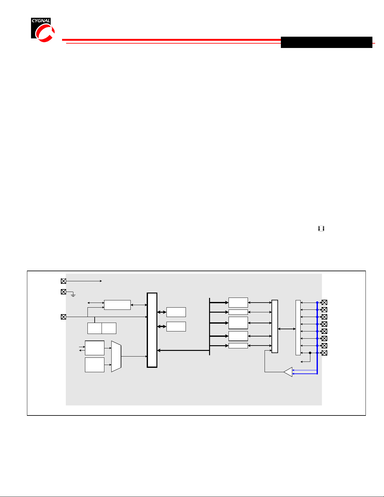
VDD
GND
/RST/C2CK
Analog/Digital
Power
C2D
XTAL1
XTAL2
POR
External
Oscillator
Circuit
Internal
Oscillator
Debug HW
Brown-
Out
Reset
System Clock
8
0
5
1
C
o
SFR Bus
r
e
8kbyte
FLASH
256 byte
SRAM
Port 0
Latch
UART
Timer 0,
1, 2 / RTC
PCA/
WDT
SMBus
X
B
A
R
CP0
P0.0
P0.1
P
0
D
r
v
C2D
+
-
P0.2/XTAL1
P0.3/XTAL2
P0.4/TX
P0.5/RX
P0.6/CNVST
P0.7/C2D
10.15.2001
C8051F303
C8051F303
C8051F303 C8051F303
8KB Flash, 256 RAM, 11-Pin MCU
PRELIMINARY
SELECTED ELECTRICAL SPECIFICATIONS T
A
= -40°C to +85°C, VDD = 2.7V unless otherwise specified.
PARAMETER CONDITIONS MIN TYP MAX UNITS
GLOBAL CHARACTERISTICS
Supply Voltage 2.7 3.6 V
Supply Current with CPU
active
Supply Current (shutdown) Oscillator off; VDD Monitor Enabled
Clock=25MHz
Clock=1MHz
Clock=32kHz; VDD Monitor Disabled
Oscillator off; VDD Monitor Disabled
5.8
0.34
11
10
<0.1
mA
mA
µA
µA
µA
CPU & DIGITAL I/O PORTS
Clock Frequency Range DC 25 MHz
Port Output High Voltage IOH = -3mA, Port I/O push-pull VDD – 0.7 V
Port Output Low Voltage IOL = 8.5mA 0.6 V
Input High Voltage 0.7 x VDD V
Input Low Voltage 0.3 x VDD V
INTERNAL OSCILLATOR
Frequency 15.0 20.0 25.0 MHz
COMPARATOR
Response Time Mode0 (CP+) – (CP-) = 100mV 0.1
Current Consumption Mode0 7.6
Response Time Mode1 (CP+) – (CP-) = 100mV 0.18
Current Consumption Mode1 3.2
Response Time Mode2 (CP+) – (CP-) = 100mV 0.32
Current Consumption Mode2 1.3
Response Time Mode3 (CP+) – (CP-) = 100mV 1
Current Consumption Mode3 0.4
µs
µA
µs
µA
µs
µA
µs
µA
PACKAGE INFORMATION
Bottom View
E2
b
LT
L
be
D3
k
e
E
Side D View
A3
A3
e
Side E View
A2
e
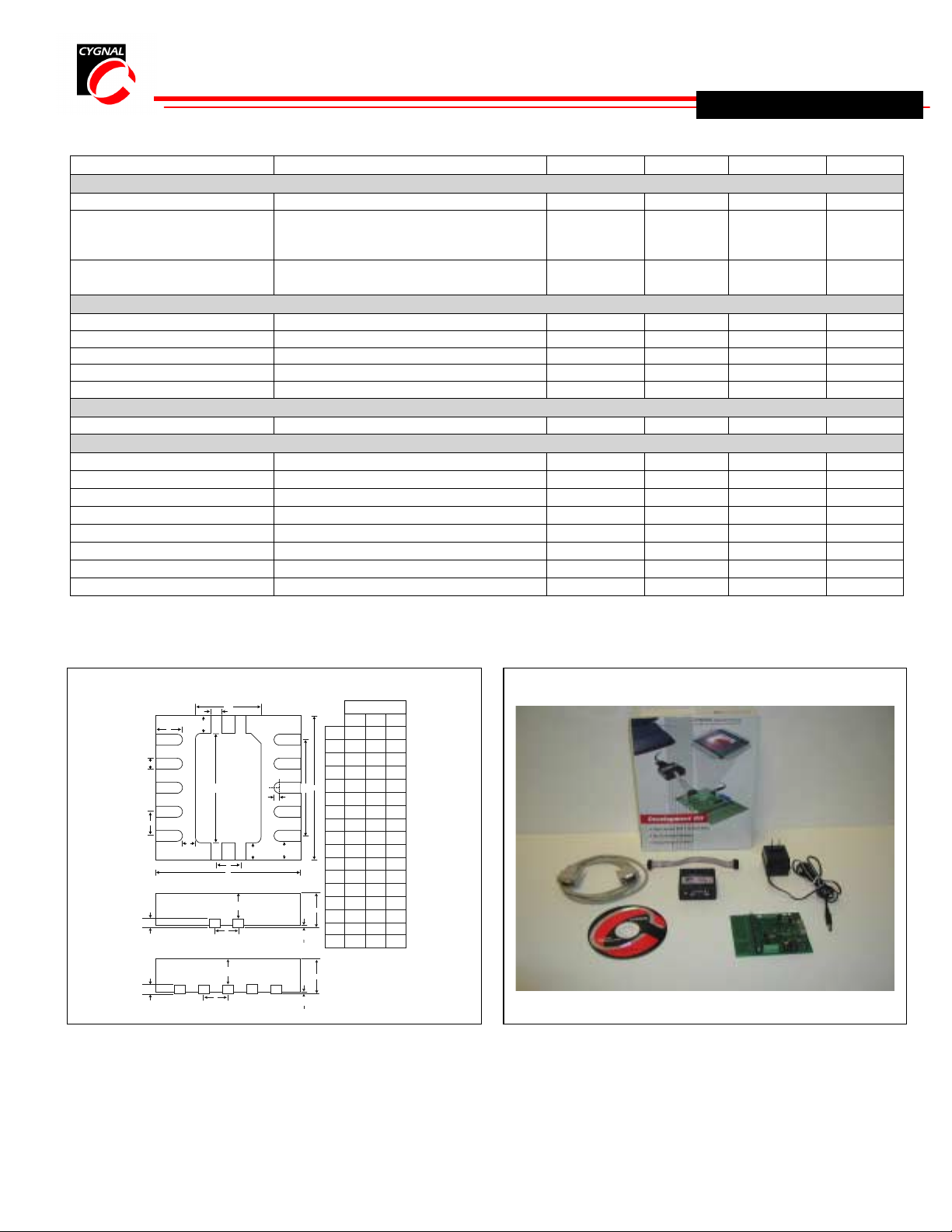
C8051F300DK DEVELOPMENT KIT
MM
MIN TYP MAX
A
0.80 0.90 1.00
A1
0 0.02 0.05
A2
0 0.65 1.00
A3
0.25
b
0.18 0.23 0.30
D
D2
R
D4
LB
A2
D
3.00
D2
0 2.20 2.25
D3
2.27
D4
0.386
E
3.00
E2
1.36
e
0.5
k
0.27
L
0.45 0.55 0.65
A
LB
0.36
LT
A1
A
A1
0.37
R
0.09
 Loading...