

CYGNL C8051F236 Datasheet
C8051F236 C8051F236 Mixed-Signal 8KB ISP FLASH MCU
PRELIMINARY
ANALOG PERIPHERALS
Two Comparators
- Programmable Hysteresis
- Configurable to Generate Interrupts or Reset
VDD Monitor and Brown-out Detector
ON-CHIP JTAG EMULATION
- On-Chip Emulation Circuitry Facilitates Full Speed,
Non-Intrusive In-Circuit Emulation
- Supports Breakpoints, Single Stepping,
Watchpoints
- Inspect/Modify Memory and Registers
- Superior Performance to Emulation Systems Using
ICE-Chips, Target Pods, and Sockets
- $99 Development Kit (C8051F236DK)
SUPPLY VOLTAGE .................... 2.7V to 3.6V
- Typical Operating Current: 9mA @ 25MHz
- Multiple Power Saving Sleep and Shutdown Modes
Temperature Range: –40 °°C to +85 °°C
48-Pin TQFP Package
8051-COMPATIBLE µµC Core
- Pipelined Instruction Architecture; Executes 70%
of Instructions in 1 or 2 System Clocks
- Up to 25MIPS Throughput with 25MHz Clock
- Expanded Interrupt Handler; Up to 22 Interrupt
Sources
MEMORY
- 1280 Bytes Data RAM
- 8k Bytes FLASH; In-System Programmable in 512
byte Sectors
DIGITAL PERIPHERALS
- 32 Port I/O; All are 5V tolerant
- Hardware SPITM and UART Serial Ports Available
Concurrently
- Three 16-bit Counter/Timers
- Dedicated Watch-Dog Timer
- Bi-directional Reset
CLOCK SOURCES
- Internal Programmable Oscillator: 2-to-16MHz
- External Oscillator: Crystal, RC, C, or Clock
- Can Switch Between Clock Sources on-the-fly;
Useful in Power Saving Modes
SPI is a trademark of Motorola, Inc.
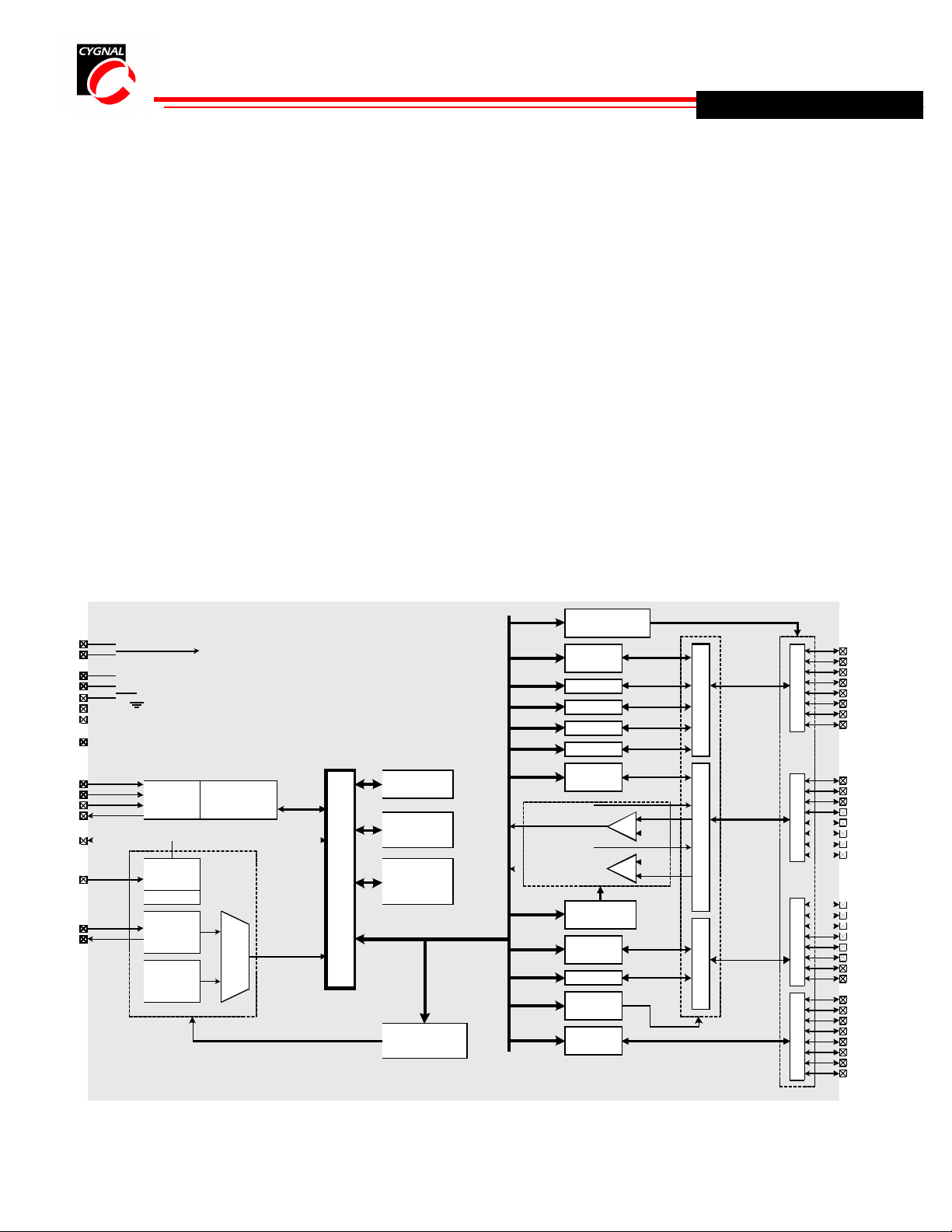
VDD
VDD
GND
GND
GND
GND
GND
N/C
TCK
TMS
TDI
TDO
/RST
MONEN
XTAL1
XTAL2
Analog/Digital
Power
JTAG
Logic
VDD
Monitor
WDT
External
Oscillator
Circuit
Internal
Oscillator
Debug HW
Reset
System Clock
8
0
5
1
C
o
SFR Bus
r
e
8kbyte
FLASH
256 byte
RAM
1024 byte
XRAM
Clock & Reset
Configuration
Port I/O Mode
& Config.
Port 0
Latch
UART
Timer 0
Timer 1
Timer 2
Port 1
Latch
CP0
CP1
CP0
CP1
Comparator
Config.
Port 2
Latch
SPI
Port Mux
Control
Port 3
Latch
CP0+
CP0-
CP1+
CP1-
P
0
M
U
X
P
1
M
U
X
P
2
M
U
X
P
0
D
r
v
P
1
D
r
v
P
2
D
r
v
P
3
D
r
v
P0.0/TX
P0.1/RX
P0.2//INT0
P0.3//INT1
P0.4/T0
P0.5/T1
P0.6/T2
P0.7/T2EX
P1.0/CP0+
P1.1/CP0P1.2/CP0
P1.3/CP1+
P1.4/CP1P1.5/CP1
P1.6/SYSCLK
P1.7
P2.0/NSS
P2.1/MISO
P2.2/MOSI
P2.3/SCK
P2.4
P2.5
P2.6
P2.7
P3.0
P3.1
P3.2
P3.3
P3.4
P3.5
P3.6
P3.7
12.20.2000
C8051F236 C8051F236 Mixed-Signal 8KB ISP FLASH MCU
PRELIMINARY
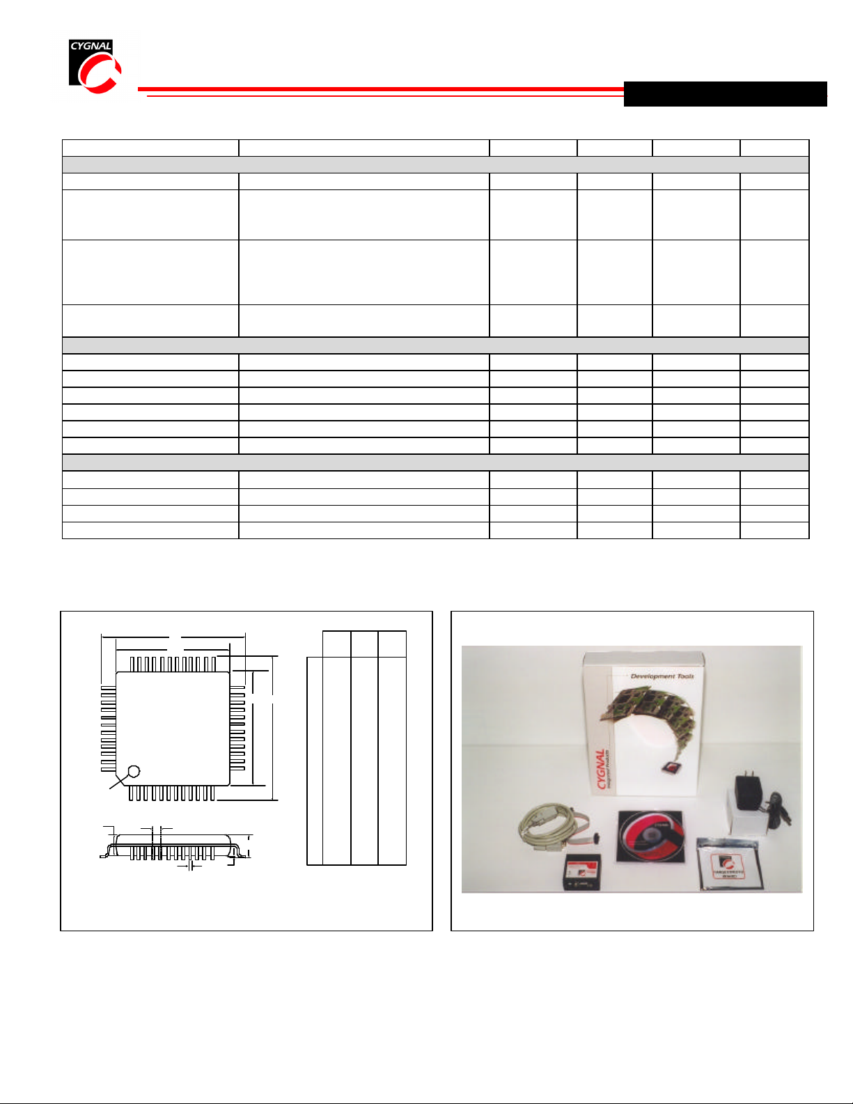
PACKAGE INFORMATION
C8051F236DK DEVELOPMENT KIT ($99)
SELECTED ELECTRICAL SPECIFICATIONS TA = -40°C to +85°C unless otherwise specified.
PARAMETER CONDITIONS MIN TYP MAX UNITS
GLOBAL CHARACTERISTICS
Digital Supply Voltage 2.7 3.6 V
Digital Supply Current with
CPU active
Digital Supply Current
(shutdown)
Digital Supply RAM Data
Retention Voltage
CPU & DIGITAL I/O PORTS
Clock Frequency Range DC 25 MHz
Port Output High Voltage IOH = -3mA, Port I/O push-pull VDD – 0.7 V
Port Output Low Voltage IOL = 8.5mA 0.6 V
Input High Voltage 0.8 x VDD V
Input Low Voltage 0.2 x VDD V
SPI Bus Clock Frequency fCLK=MCU Clock; SPI in Master Mode fCLK/2 MHz
COMPARATORS
Response Time | CP+ – CP- | = 100mV 4
Input Voltage Range -0.25 VDD + 0.25 V
Input Bias Current -5 0.001 +5 nA
Input Offset Voltage -10 +10 mV
Clock=25MHz
Clock=1MHz
Clock=32kHz
Oscillator not running; VDD Monitor
Enabled
Oscillator not running; VDD Monitor
Disabled
9
0.4
18
7
0.1
mA
mA
µA
µA
µA
1.5 V
µs
D
D1
48
PIN 1
IDENTIFIER
A2
1
e
A1
b
MIN
NOM
(mm)
-
-
1.00
0.22
9.00
7.00
0.50
9.00
7.00
MAX
(mm)
1.20
0.15
1.05
0.27
-
-
-
-
-
(mm)
A
-
A1
A2
D
D1
E
E1
0.05
0.95
b
0.17
-
-
e
-
-
-
EE1
A
 Loading...