

Page 1

COMPACTPCI-824
FEP BLADE INTELLIGENT
I/O CONTROLLER
USER’ S MANUAL
The information in this document has been carefully checked and is believed to be entirely reliable. However, no
responsibility is assumed for inaccuracies. Furthermore, Cyclone Microsystems, Inc. reserves the right to make
changes to any products herein to improve reliability, function, or design. Cyclone Microsystems, Inc. neither
assumes any liability arising out of the application or use of any product or circuit described herein, nor does it
convey any license under its right or the rights of others.
Revision 1.0, January 2006
Cyclone P/N 800-0824
Copyright 2005 by Cyclone Microsystems, Inc.
Page 2

CONTENTS
CHAPTER 1
1.1 INTRODUCTION..............................................................................................................................1-1
1.2 FEATURES ......................................................................................................................................1-2
1.3 SPECIFICATIONS............................................................................................................................1-3
1.4 ENVIRONMENTAL...........................................................................................................................1-3
1.5 REFERENCE MANUALS.................................................................................................................1-5
1.6 SOFTWARE DEVELOPMENT.........................................................................................................1-6
CHAPTER 2
2.1 AMCC POWERPC 440GX PROCESSOR.......................................................................................2-1
2.2 BYTE ORDERING............................................................................................................................2-1
2.3 MEMORY MAP........................ ... ... ... .... ... ... ... ....................................... ... ... .... ... ... ... .... .....................2-2
2.4 DDR SDRAM INTERFACE ..............................................................................................................2-2
2.4.1 Installation and Removal of Memory Modules.....................................................................2-3
2.5 INTERRUPTS...................................................................................................................................2-3
2.5.1 External Interrupts...............................................................................................................2-4
2.6 CONSOLE SERIAL PORT...................................................... ... .... ... ... ... ... .... ..................................2-4
2.7 ETHERNET......................................................................................................................................2-5
2.7.1 Gigabit Ethernet Port...........................................................................................................2-5
2.7.2 Gigabit Ethernet LEDs.........................................................................................................2-6
2.7.3 Fast Ethernet Port ...............................................................................................................2-6
2.7.4 Fast Ethernet LEDs .............................................................................................................2-6
2.8 PERIPHERAL BUS ..........................................................................................................................2-7
2.8.1 Flash ROM ..........................................................................................................................2-7
2.8.2 LEDs....................................................................................................................................2-7
2.8.3 User LEDs During Initialization............................................................................................2-7
2.8.4 Georgraphic Addressing.......................... ... ....................................... ... ... ... .... ... ... ... ... .... ... ..2-8
2.8.5 Power Supply Monitoring.....................................................................................................2-9
2.9 FAN MONITORING..........................................................................................................................2-9
2
2.10 I
C BUS......... ... ... ....................................... ... ... .... ... ... ... .... ...................................... .... .....................2-9
2.10.1 SDRAM EEPROM.............................................................................................................2-10
2.10.2 Temperature Sensors.................... ... ... .... ... ... ... .................................................................2-10
2.10.3 Serial EEPROM.................................................................................................................2-10
2.10.4 Phase Lock Loop Clock Driver ..........................................................................................2-10
2.11 JTAG EMULATOR SUPPORT.......................................................................................................2-10
APPENDIX A
A.1 INTRODUCTION............................................................................................................................. A-1
A.2 PHYSICAL ATTRIBUTES ............................................................................................................... A-1
A.3 PMC MODULE SIGNAL DEFINITIONS .......................................................................................... A-1
A.4 PMC MODULE CONNECTOR........................................................................................................ A-2
APPENDIX B
B.1 INTRODUCTION............................................................................................................................. B-1
CPCI-824 User’s Manual i
Revision 1.0., January 2006
Page 3

CONTENTS
LIST OF FIGURES
Figure 1-1. CPCI-824 Block Diagram ....................................................................................................1-1
Figure 1-2. CPCI-824 Physical Configuration........................................................................................1-4
Figure 2-1. CPCI-824 Memory Map.......................................................................................................2-2
Figure 2-2. LED Register Bitmpa, E800 0001H.....................................................................................2-7
Figure 2-3 Geographic Addressing Register, B800 0001h.......................................................... .... ... ..2-8
Figure 2-4 Power Supply Status Register, E000 0000H.......................................................................2-9
LIST OF TABLES
Table 1-1. CPCI-824 Power Requirements .........................................................................................1-3
Table 1-2. Environmental Specifications .. ... ... ... ...................................................................................1-3
Table 2-1. SDRAM Configurations .................................... .... ... ... ... .... ... ... ... ... ......................................2-3
Table 2-2. External Interrupts ................................... ... ... ... .... ... ... .......................................... ...............2-4
Table 2-3. Console Serial Port Connector............................................................................................2-5
Table 2-4 Gigabit Port Connector........................................................................................................2-5
Table 2-5 10/100 Fast Port Connector ................................................................................................2-6
Table 2-6 Breeze Start-up LEDs................. ... ... ... .... ... ... ... .... ... ... ... .... ......................................... .........2-8
Table 2-7 I
2
C Device Addresses .......................................................................................................2-10
Table 2-8 JTAG Emulator Pin Assignment. ... ... ... .... ... ... ... .... ... ... ... .... ... ... ... ... .... ... .............................2-11
Table A-1. PMC Clock & Arbitration Assignment................................................................................. A-2
Table A-2. PMC Interrupt Assignment ................................................................................................. A-2
Table A-3. P21 PMC Module Connector Pinout...................................................................................A-3
Table A-4. P22 PMC Module Connector Pinout...................................................................................A-4
Table A-5. P23 PMC Module Connector Pinout...................................................................................A-5
Table B-1. CPCI-821 J2 Definition........................ .... ... ... ... .... ... ... ... .... ... ... ... ........................................ B-1
CPCI-824 User;s Manual ii
Revision 1.0., January 2006
Page 4

CONTENTS
LIST OF FIGURES
Figure 1-1. CPCI-824 Block Diagram ....................................................................................................1-1
Figure 1-2. CPCI-824 Physical Configuration........................................................................................1-4
Figure 2-1. CPCI-824 Memory Map.......................................................................................................2-2
Figure 2-2. LED Register Bitmpa, E800 0001H.....................................................................................2-7
Figure 2-3 Geographic Addressing Register, B800 0001h.......................................................... .... ... ..2-8
Figure 2-4 Power Supply Status Register, E000 0000H.......................................................................2-9
LIST OF TABLES
Table 1-1. CPCI-824 Power Requirements .........................................................................................1-3
Table 1-2. Environmental Specifications .. ... ... ... ...................................................................................1-3
Table 2-1. SDRAM Configurations .................................... .... ... ... ... .... ... ... ... ... ......................................2-3
Table 2-2. External Interrupts ................................... ... ... ... .... ... ... .......................................... ...............2-4
Table 2-3. Console Serial Port Connector............................................................................................2-5
Table 2-4 Gigabit Port Connector........................................................................................................2-5
Table 2-5 10/100 Fast Port Connector ................................................................................................2-6
Table 2-6 Breeze Start-up LEDs................. ... ... ... .... ... ... ... .... ... ... ... .... ......................................... .........2-8
Table 2-7 I
2
C Device Addresses .......................................................................................................2-10
Table 2-8 JTAG Emulator Pin Assignment. ... ... ... .... ... ... ... .... ... ... ... .... ... ... ... ... .... ... .............................2-11
Table A-1. PMC Clock & Arbitration Assignment................................................................................. A-2
Table A-2. PMC Interrupt Assignment ................................................................................................. A-2
Table A-3. P21 PMC Module Connector Pinout...................................................................................A-3
Table A-4. P22 PMC Module Connector Pinout...................................................................................A-4
Table A-5. P23 PMC Module Connector Pinout...................................................................................A-5
Table B-1. CPCI-821 J2 Definition........................ .... ... ... ... .... ... ... ... .... ... ... ... ........................................ B-1
CPCI-824 User;s Manual ii
Revision 1.0., January 2006
Page 5
1.1 INTRODUCTION
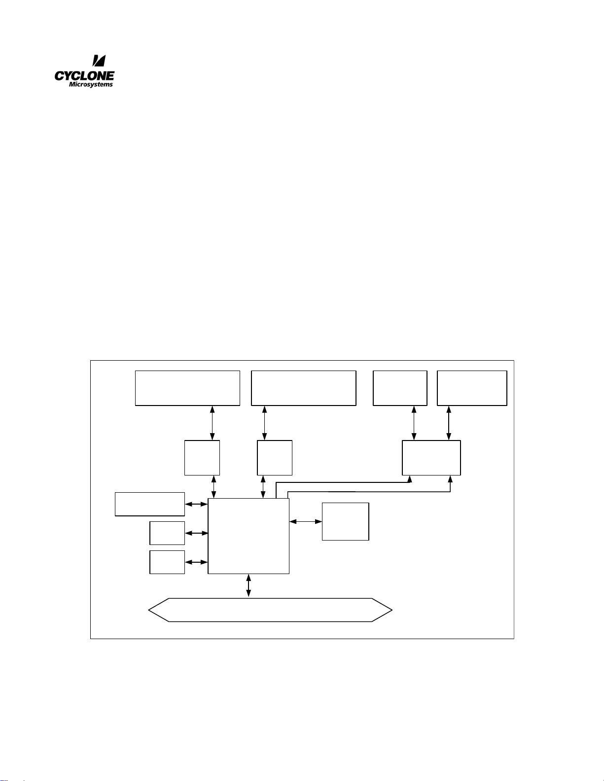
The CompactPCI-824 is a Hot Swap Intelligent I/O Controller.
The CPCI-824 card is based on the AMCC™ PowerPC™ 440GX, which is AMCC’s next generation
integrated processor based on the PowerPCI 440 core operating at a frequency of 667 MHz. The 440GX
supplies memory controller functions with up to 512 Mbytes of DDR SDRAM (64-bit with ECC) on an
SoDIMM module at 333 MHz DDR. The PowerPC core with 256K L2 cache, the memory controller,
the PCI-X Bridge, and the DMA controller of AMCC 440GX are among the features on the Processor
local bus operating at 128-bit and a frequency of 166 MHz. The 440GX Peripheral Bus (EPC) has three
devices; 8 Mbytes of Flash ROM, software LEDs, and external revision control registers. Additionally,
the 440GX contains four Ethernet MACs. Four Ethernet ports are provided on the CPCI-824. Two are
10/100/1Gb ports configured as RGMII and two are 10/100 Mbps ports and reconfigured as SMII. The
CPCI-824 also utilized one of the I2C bus interface units, and one of the two UART units. A block
diagram of the CPCI-824 is shown on Figure 1-1.
CHAPTER 1
GENERAL INTRODUCTION
Figure 1-1. CPCI-824 Block Diagram
DDR SDRAM
333 MHz
Flash
ROM
JTAG
10/100/1000
Ethernet Port
PHY PHY PHY
I/F
AMCC PPC440GX
MHz
Local Bus PCI-X
10/100/1000
Ethernet Port
Console
Serial
Port
10/100
Ethernet
Port
10/100
Ethernet Port
CPCI-824 User’s Manual 1-1
Revision 1.0, January 2006
Page 6

GENERAL INTRODUCTION
1.2 FEATURES
•PowerPC™ Processor An AMCC 440GX embedded processor based on the AMCC
PowerPC superscalar core. It operates at a maximum frequency of
667 MHz internally.
• SD RAM Up to 512 MByte of 333 MHz DDR SDRAM is supported via a 200
pin SoDIMM module.
• Flash ROM 8 Mbytes of in-circuit sector-programmable Flash ROM provides
non-volatile storage on the CPCI-824. One 128 Kbyte sector of the
Flash ROM is reserved for the storage of non-volatile boot and
system parameters. System calls for storing parameters in this
memory are included in the Breeze Development Environmentª
• Con sole Serial Port An asynchronous serial port based on a 16C750 UART with an RS232 interface is provided for a console terminal or workstation
connection.
• Ethernet Ports Two 10/100/1Gb Base-TX Ethernet ports are provided. Each port
supports up to 1Gbps and uses a RJ45 style modular phone jack. The
MAC contained within the 440GX interfaces with 2 Broadcom
BMC5461S PHY transceivers.
Two 10/100 Base-TX Ethernet ports. Each supports u p to 1 00 Mbps
and also uses a RJ45 style modular phone jack. In this case the MAC
contained within the 440GX interfaces with a Broadcom BCM5248.
The BCM5248 is an eight port PHY, but we are only using the first 2
ports.
• Temperature Sensors Two LM75 type programmable temperature sensors with interrupt
signaling capability are provided for system monitoring purposes.
•I
O Messaging The CPCI-824 supports the I2O specification for interprocessor
2
communication.
• DMA Controller The 440GX supports 4 separate DMA channels for high throu ghput
data transfers between PCI bus agents and the local SDRAM
memory.
• Breeze Development
Environment™
Flash-resident ROM monitor / firmware package which supports
board-level initialization and application software development.
More information on the Breeze Development Environment™ can
be found in Breeze Developer’s Manual.
• Blade Style Interface The CPCI-824 receives power, fan detect, power supply status and
geographic addressing from J1 and J2. Note that the fan detect and
power supply status signals are only available when a CPCI-824 is
installed in the system slot.
• Hot Swap The CPCI-824 is a Basic Hot Swap board, compliant with PICMG
2.1.
1-2
CPCI-824 User’s Manual
Revision 1.0, January 2006
Page 7
1.3 SPECIFICATIONS
GENERAL INTRODUCTION
Physical Characteristics The CPCI-824 is a single slo t, double high CompactPCI
™
card with a
peripheral slot interface. This product is equipped with an AMCC
PowerPC 440GX mcroprocessor.
Height 9.187” (233.35mm)
Double Eurocard (6U)
Depth 6.299” (160mm)
Width .8” (20.32mm)
Power Requirements The CPCI-824 requires +5V, +12V, -12V and +3.3V from the
CompactPCI
™
backplane J1 connector. The card is Universal and
support either +3.3V or +5V V(I/O).
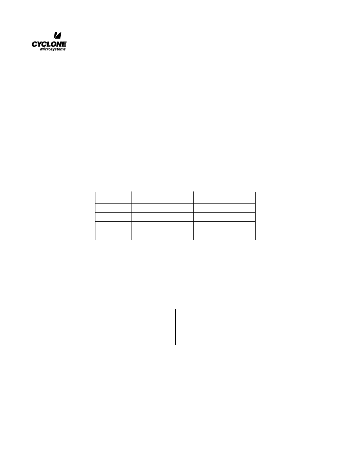
Table 1-1. CPCI-824 Power Requirements
Voltage Current Typical Current Maximum
+3.3V 3.49 Amps 4.99 Amps
+5V 0.03 Amps 0.04 Amps
+12V 0.01 Amps 0.02 Amps
-12V 0.02 Amps 0.03 Amps
1.4 ENVIRONMENTAL
A small amount of airflow will be required, such as is found in a typical Eurocard enclosure.
Table 1-2. Environmental Specifications
Operating Temperatures 0 to 55 Degrees Celsius
Relative Humidity
(non-condensing)
0-95%
Storage Temperatures -55 to 125 Degrees Celsius
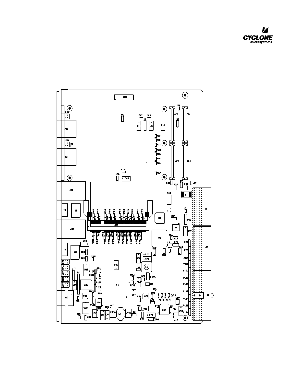
Figure 1-2 is a physical diagram (not to scale) of the CPCI-824 adapter, showing the location
designators of jumpers, connectors, and major ICs. Refer to this figure when component locations are
referenced in the manual text.
CPCI-824 User’s Manual 1-3
Revision 1.0, January 2006
Page 8
GENERAL INTRODUCTION
Figure 1-2. CPCI-824 Physical Configuration
1-4
CPCI-824 User’s Manual
Revision 1.0, January 2006
Page 9

1.5 REFERENCE MANUALS
PowerPC 440GX Processor
User’s Manual, Document#
Data Sheet, Document #
GENERAL INTRODUCTION
Applied Micro Circuits Corporation
6290 Sequence Drive
San Diego, CA 92121
(800) 755-2622
http://www.amcc.com
RC28F640J3 Strata Flash Data Sheet
Developer’s Manual, Document #278848
Data Sheet, Document #278821
Intel Corporation
Literature Sales
P.O. Box 7641
16215 Alton Parkway
Irvine, CA 92619-7013
http://www.broadcom.com
LM75 Digital Temperature Sensor National Semiconductor
2900 Semiconductor Drive
P.O. Box 58090
Santa Clara, CA 95052-8090
(800) 272-9959
http://www.national.com
CompactPCI
3.0
™
Specification PICMG 2.0R
PCI Industrial Computers Manufacturing Group
401 Edgewater Place, Suite 500
Wakefield, MA 01880
(781) 224-1100
(781) 224-1239 Fax
www.picmg.org
PCI Local Bus Specification, Revision 2.2
PCI special Interest Group
5440 SW Westgate Dr. Suite #217
PCI-X Addendum Rev 1.0
Portland, OR 97221
(800) 433-5177 (U.S.)
(503) 222-6190 (International)
(503)222-6190 (Fax)
[email protected]
Breeze for XScale 80331 Developer’s
Manual
Part Number 850-0151
Cyclone Microsystems Inc.
370 James Street
New Haven, CT 06513
(203) 786-5536
http://www.cyclone.com
2
I
0 Specification, Revision 1.0 I20 Special Interest Group
(415) 750-8352
http://www.i2osig.org
CPCI-824 User’s Manual 1-5
Revision 1.0, January 2006
Page 10

GENERAL INTRODUCTION
JTAG Debugger Wind River HSI
500 Wind River Way
Alameda, CA 94501
(510) 748-4100
http://www.windriver.com
1.6 SOFTWARE DEVELOPMENT
To simplify software development, Cyclone Microsystems has created the Breeze Development
Environment
TM
. Breeze includes initialization routines, hardware control routines and functions which
provide a simple interface to the PCI bus. Source code for accessing the Breeze Development Environ-
TM
ment
is included with the CPCI-824, allowing Breeze functions to be incorporated in a real-time
operating system as well.
The Breeze Development Environment
TM
has been designed to make the development cycle on the
CPIC-713 as simple as possible. Source code provided for Breeze also acts as example code to aid
developers in creatnig their own applications. Breeze is present on all CPCI-824 systems and its
debugging facilities are available during the development cycle.
Breeze for the CPCI-824 has been developed with the aid of the Wind River HSI VisionPROBE
software debugger and VisionCLICK user interface. The VisionPROBE degugger communicates with
a JTAG port on the C PCI-824. It provides the capability to download user code to Flash ROM or
SDRAM. It is recommended that developers obtain a set of these tools or their equivalents to support
application code development.
A complete description of the Breeze Development Environment
TM
can be found in the “Breeze for
PowerPC 440GX Developer’s Manual”, see Section 1.5, Reference Manuals.
1-6
CPCI-824 User’s Manual
Revision 1.0, January 2006
Page 11

2.1 AMCC POWERPC 440GX PROCESSOR
The AMCC PowerPC 440GX Embedded Processor is a member of AMCC’s PowerPC 400 family of
microprocessors. The 440GX on the CPCI-824 combines a powerful 667 MHz PowerPC core with
intelligent peripherals and is designed to optimize I/O processing tasks. The 440GX processor consolidates into a single system:
• AMCC PowerPC core.
• 256 Kbyte L2 Cache.
•32 Kbyte Data and Instruction Caches.
•PCI-X interface.
•High-Performance Memory Controller
•Interrupt Controller with 18 external interrupt inputs.
•Four Direct Memory Access (DMA) Controllers.
•Two 10/100/1Gb Ethernet ports with TCP/IP acceleration hardware (TAH)
•Two 10/100Mb Ethernet ports.
•Messaging Unit
•External Bus Control (EBC) interface.
2
•Two I
• Tw o 16750 compatible UARTS.
• Thirty two General Purpose Input Output (GXIO) ports.
C Bus Interface Units.
HARDWARE
CHAPTER 2
HARDWARE
For detailed descriptions of the 440GX, including programming information, consult the AMCC
PowerPC 440GX User’s Manual.
2.2 BYTE ORDERING
The CPCI-824 is configured to access external devices in big endian mode. The byte ordering determines
which memory location stores the least significant byte of the operand. Big endian stores the most significant byte in the lowest address.
CPCI-824 User’s Manual 2-1
Revision 1.0, January 2006
Page 12
HARDWARE
2.3 MEMORY MAP
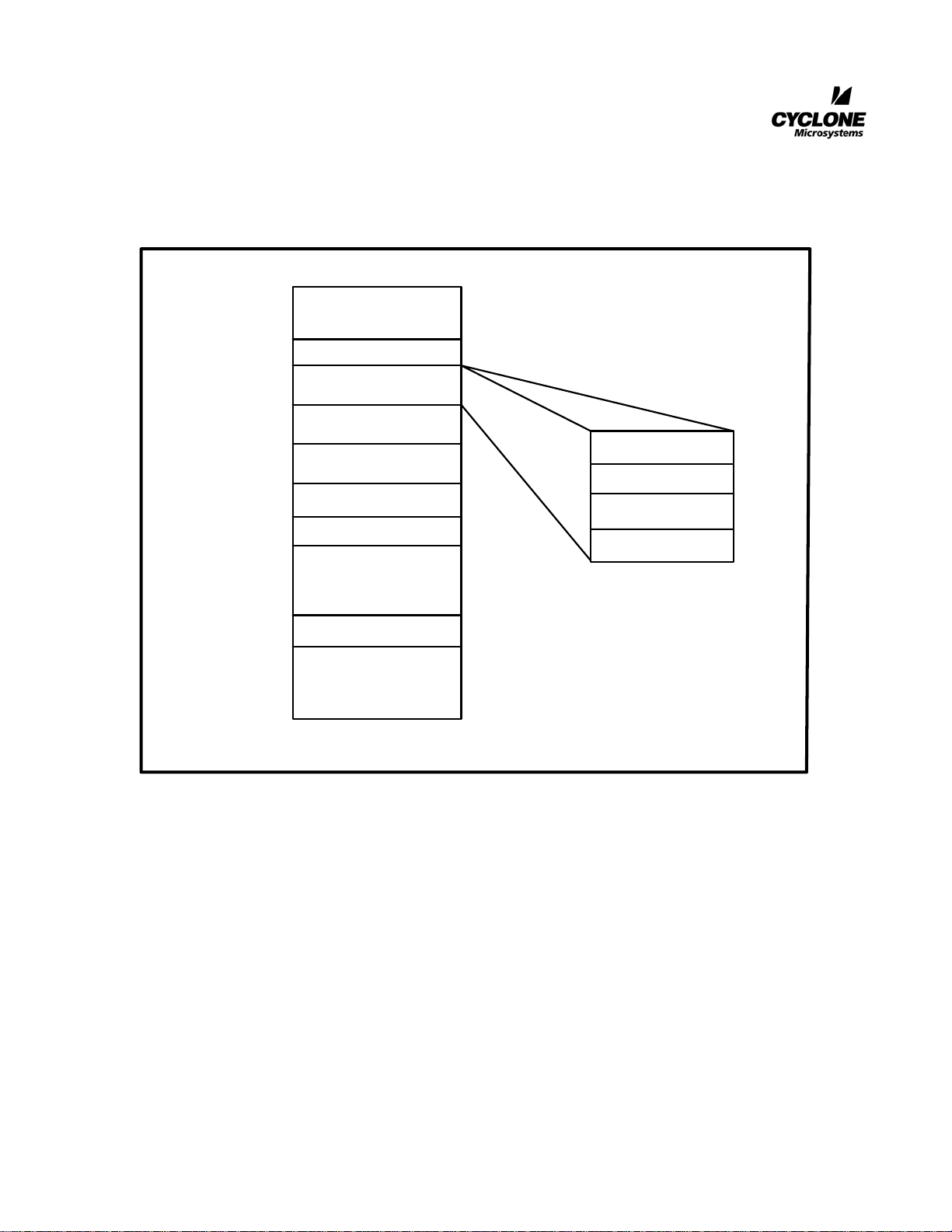
Figure 2-1 shows the CPCI-824 memory map, as configured by Breeze firmware.
FFFF FFFFh
FF80 0000h
F000 0000h
E000 0000h
D000 0000h
C000 0000h
8000 0000h
6000 0000h
4000 0000h
2000 0000h
0000 0000h
FLASH ROM
UNUSED
PERIPHERALS
PCI I/O
INTERNAL SRAM
PCI Memory
UNUSED
DDR*
SDRAM
NON-CACHEABLE
UNUSED
DDR*
SDRAM
CACHEABLE
Local PCI
Interrupts (Read Only)
LED Register
(Write Only)
Geographic Address
(Read Only)
Power Supply Status
(Read Only)
* These are physically the
same locations
E800 0002h
E800 0001h
E800 0001h
E800 0000h
Figure 2-1. CPCI-824 Memory Map
2.4 DDR SDRAM INTERFACE
The CPCI-824 is equipped with a 200 pin SoDIMM socket formatted to accept +2.5V synchronous
double data rate DRAM (DDR SDRAM) with or without Error Correction Code (ECC). The socket will
accept DDR SDRAM from 64 Mbytes to 1 Gbyte. The SDRAM is accessible from the host PCI bus.
The CPCI-824 uses 72-bit DDR SDRAM with ECC or 64-bit DDR SDRAM without ECC. DDR
SDRAM allows zero data-to-data wait state operation w ith an effective data transfer rate of 333 MHz.
The CPCI-824 is shipped with unbuffered ECC DDR SDRAM installed in the SoDIMM socket. The
memory may be expanded by inserting up to a 1 GByte module into the 200 pin SoDIMM socket. The
various memory combinations are shown in Table 2-1. Only 200 pin, one or two bank, +2.5V DDR
SDRAM modules with or without ECC rated as PC2700 or faster should be used on the CPCI-824.
2-2
CPCI-824 User’s Manual
Revision 1.0, January 2006
Page 13

Table 2-1. SDRAM Configurations
HARDWARE
DDR
SDRAM
Technology
DDR SDRAM
Arrangement# Banks
Row Column
Total
Memory Size
128 Mbit 16M x 8 bit 1 12 10 128 Mbyte
2 12 10 256 Mbyte
8M x 16 bit 1 12 9 64 Mbyte
2 12 9 128 Mbyte
256 Mbit 32M x 8 bit 1 13 10 256 Mbyte
2 13 10 512 Mbyte
16M x 16 bit 1 13 9 128 Mbyte
2 13 9 256 Mbyte
512 Mbit 64M x 8 bit 1 13 11 512 Mbyte
2 13 11 1 Gbyte
32M x 16 bit 1 13 10 256 Mbyte
2 13 10 512 Mbyte
2.4.1 Installation and Removal of Memory Modules
Installation or removal of SoDIMM memory on the CPC I-824 is a simple procedure and requires no
special tools. The CPCI-824 should be removed from the host system before changing a memory
module and care must be taken to avoid static discharge while contacting the board. A properly
connected grounding strap should be worn while installing or removing memo ry modules on the CPCI824 adapter.
Memory modules are removed by rotating the latches located on each end of the SoDIMM socket
outward, away from the module. As the latches are moved outward, the module will pop up, partially
out of the socket. Grasp the module by its edges and slide it out of the socket.
To in stall a memory module, first id entify its proper orientation. Each module is ke yed with a notch in
the card edge of the circuit board that corresponds to a tab in the socket. With the correct orientation
established, hold the module at an angle to the surface of the CPCI-824 and insert the module into the
card edge receptacle on the socket. When the module is fully inserted (the gold contacts on the module
will not be visible) press down on the high edge of the module until it snaps behind the latches.
2.5 INTERRUPTS
An Interrupt is the action in which th e PPC440GX saves its old context (Machine State Register (MSR)
and next instruction address) and begins execution at a pre-determined interrupt-handler address, with a
modified MSR. Exceptions are the events that may cause the processor to take an interrupt, if the corresponding interrupt type is enabled.
CPCI-824 User’s Manual 2-3
Revision 1.0, January 2006
Page 14
HARDWARE
Exceptions may be generated by the execution of instructions, or by si gns from devices external to the
PPCI440GX, the internal timer facilities, debug events, or error conditions.
All interuupts, except for Machine Check, can be categorized according to two independent characteristics of the interrupt. They are asynchronous or synchronous and critical and non-critical.
Asynchronous interrupts are caused by events that are independent of instruction execution. For
asynchronous interrupts, the address reproted to the interrupt handling routine is the address of the
instruction that would have executed next, had the asynchronous interrupt not occurred. Synchronous
interrupts are those that are caused directly by the execution (or attempted execution) of instructions.
Critical interrupt and non-critical interrupts use different save/restore register pairs. Machine check
interrupts are typically caused by some kind of hardware or storage subsystem failure, or by an attempt
to access an invalid address.
2.5.1 External Interrupts
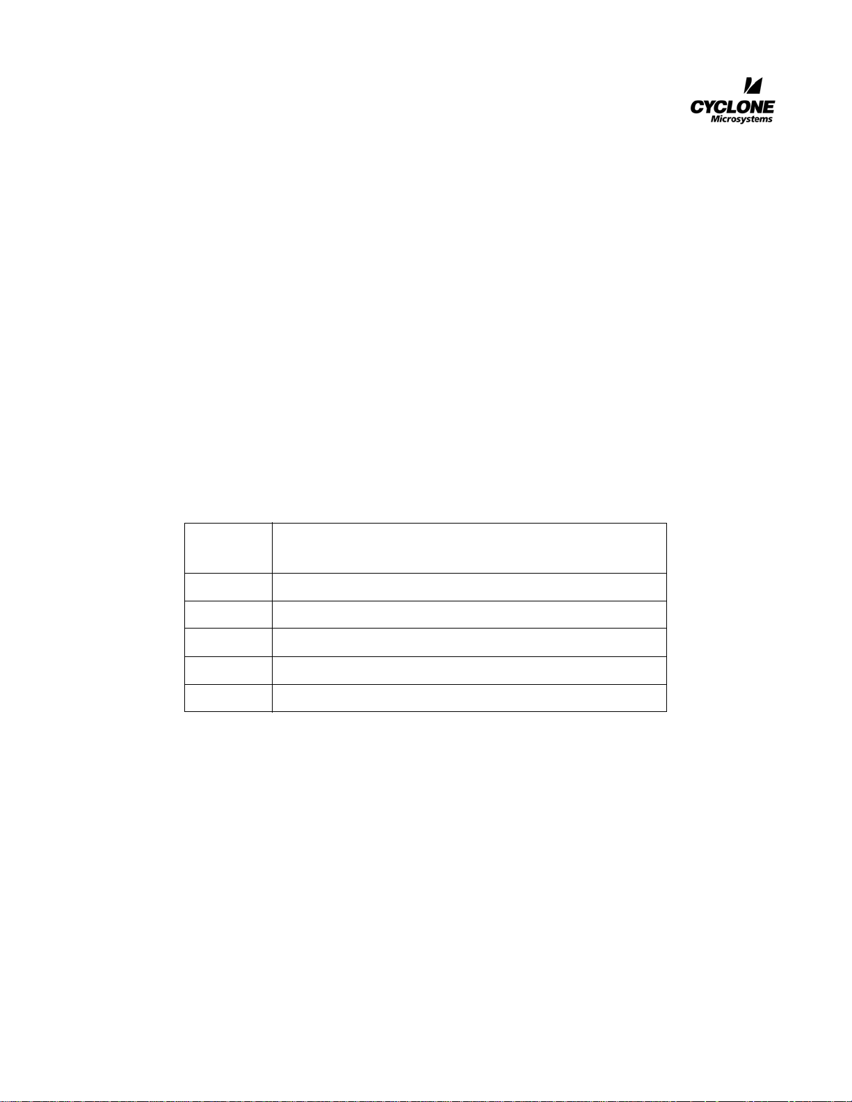
On the CPCI-824, the external interrupts are connected to t he PPC440GX as shown in Table 2-2. The
local PCI interrupts are shared. Therefore, to determine which of the four local PCI interrupts caused
the interrupt, a local board register is provided at address E800 0002h.
Table 2-2. External Interrupts
Interrupt
Input
IRQ6 TEMPERATURE INTERRUPT
IRQ7 FAN 0 INTERRUPT
IRQ8 FAN 1 INTERRUPT
IRQ9 POWER GOOD INTERRUPT
IRQ10 LOCAL PCI BUS INTERRUPT
2.6 CONSOLE SERIAL PORT
The CPCI-824 adapter utilizes the first of the two UART units of the 440GX. The console serial port
with an RS-232 line interfaces has been included on the CPCI-824. The port is connected to a RJ-11
type phone jack on the adapter and can be connected to a host system using the included phone jack to
DB-25 cable (Cyclone P/N 530-2006)
The serial port is capable of operating at speeds from 300 to 115200 bps and can be operated in
interrupt-driven or polled mode. Breeze firmware uses serial settings of 9600 bps, 8 bit data, no parity,
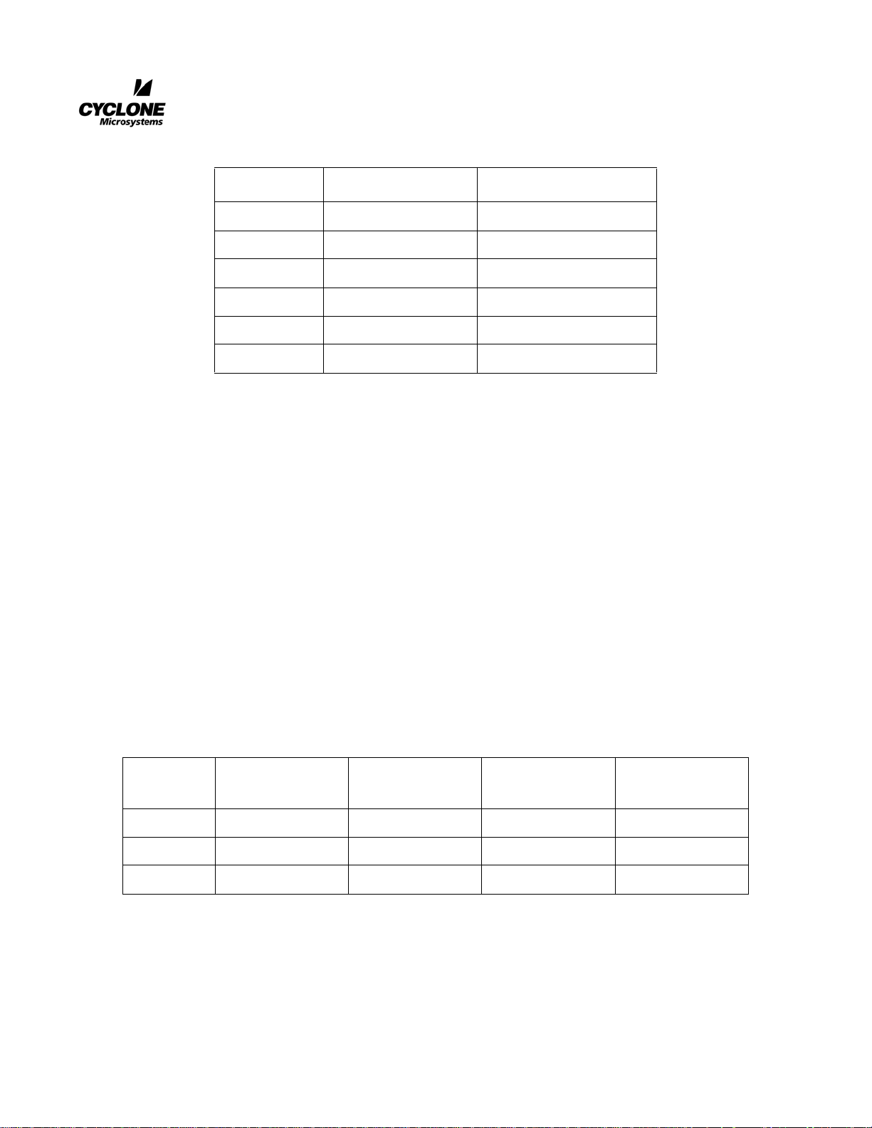
one stop bit, and no flow control. (9600-8N-1). The console serial port connector pin assignment is
shown in Table 2-3.
Interrupt Type
2-4
CPCI-824 User’s Manual
Revision 1.0, January 2006
Page 15
2.7 ETHERNET
The CPCI-824 has two 1 Gigabit Ethernet ports for CAT5 UTP (category 5 unshielded twisted pair).
The CPCI-824 1 Gigabit Ethernet is based on the 10/100/1G Ethernet MAC contained in the 440GX
and the Broadcom BCM5461 Gigabit Transciever (PHY). The interface between the MAC and PHY is
RGMII. The BCM5461 automatically negotiates with its link partner to determi ne the highest possible
operating speed. The two 10/100 Mbps Ethernet ports interface between the MAC contained within the
440GX and a Broadcom BCM5248 octal 10/100 Mbit PHY. Only two of the BCM5248 ports are used
in an SMII configuration.
HARDWARE
Table 2-3. Console Serial Port Connector
Pin Signal Description
1 N/C Not Used
2 GND Signal Ground
3 TXD Transmit Data
4 RXD Receive Data
5 N/C Not Used
6 N/C Not Used
2.7.1 Gigabit Ethernet Port
The copper line interface of each Gigabit Ethernet port is a shielded RJ45 (modular phone type)
connector. The connector conforms to the 1000/100/10Base-T specification. The aggregated input and
output ports exit the panel of the CPCI-824.
Note that in 10Base-T and 100Base-T mode, only two pairs are used, one for transmit data and one for
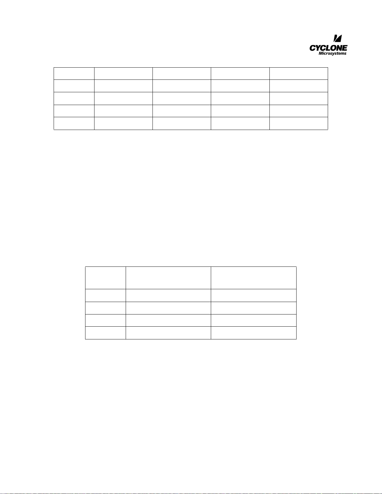
receive data. The pin assignment of copper port 0 (J13) and port 1 (J11) is shown on Table 2-4.
Pin
Signal
(10/100Base-T)
11 TX+ Output TRD0+ Input/Output
10 TX- Output TRD0- Input/Output
4 RX+ Input TRD1+ Input/Output
Table 2-4. Gigabit Port Connector
Description
(10/100Base-T)
Signal
(1000Base-T)
Description
(1000Base-T)
CPCI-824 User’s Manual 2-5
Revision 1.0, January 2006
Page 16
HARDWARE
5 RX- Input TRD1- Input/Output
3 Not Used TR2+ Input/Output
2 Not Used TRD2- Input/Output
8 Not Used TRD3+ Input/Output
9 Not Used TRD3- Input/Output
2.7.2 Gigabit Ethernet Port LEDs
Both of the Gigabit Ethernet prots of the CPCI-824 have LEDs associated with the connector. The ports
have the LEDs built into the RJ45 connectors. The “LNK” LED indicates, when lit, that the port is
LINKed to a functional ethernet network. The “ACT” LED indicates, when lit, that there is ACTivity
of transmit or receive data. Normal operation on a 1000Base-T network would have the “LNK” LED lit
and the “ACT” LED flashing.
2.7.3 Fast Ethernet Port
The copper line interface of each 10/100 Mbit Fast Ethernet port is a shielded RJ45 (modular phone
type) connector. The aggregated input and output ports exit the panel of the CPCI-824.
The pin assignment of Port 0 (J8) and port 1 (J5) is shown on Table 2-5.
Table 2-5. 10/100 Fast Port Connector
Pin
1 TX+ Output
2 TX- Output
3RX+ Input
6RX- Input
2.7.4 Fast Ethernet Port LEDs
Both of the Fast Ethernet ports of the CPCI-824 have LEDs associated with the connector. The ports
have the LEDs adjacent to the RJ45 connectors. The “LNK” LED indicates, when lit, that the port is
LINKed to a functional ethernet network. The “ACT” LED indicates, when lit, that there is ACTivity
of transmit or receive data. Normal operation on a 10/100 Base-T network would have the “LNK” LED
lit and the “ACT” LED flashing.
Signal
(10/100Base-T)
Description
(10/100Base-T)
2-6
CPCI-824 User’s Manual
Revision 1.0, January 2006
Page 17
2.8 PERIPHERAL BUS
The CPCI-824 utilizes the 440GX External Bus Controller (EBC) as a data communication path to the
Flash memory and other peripheral devices such as LEDs and the CPLD for the external register
control. The address/data path is on a programmable 8-bit width bus and operates at high bandwidth.
2.8.1 Flash ROM
The CPCI-824 provides 8 Mbytes of sector-programmable Flash ROM for non-volatile code storage.
The CPCI-824 Flash ROM is an Intel Strataflash J3 type-device, 8 (28F640J3) MBytes in size. The
width of the flash bus is 8 bits.
On the CPCI-824, the Flash ROM is mapped beginning at address FF80 0000h , and is divided into four
separate memory regions by Breeze firmware: boot region, flash file system, free flash, and boot
parameter region. The mapping ensures that, after a reset, the processor can begin execution at the reset,
the processor can begin execution at the reset vector address FFFF FFFCh. The size and start location
of each of these regions is defined by Breeze software. Refer to the Breeze for 440GX Developer’s
Manual for more information.
2.8.2 LEDS
HARDWARE
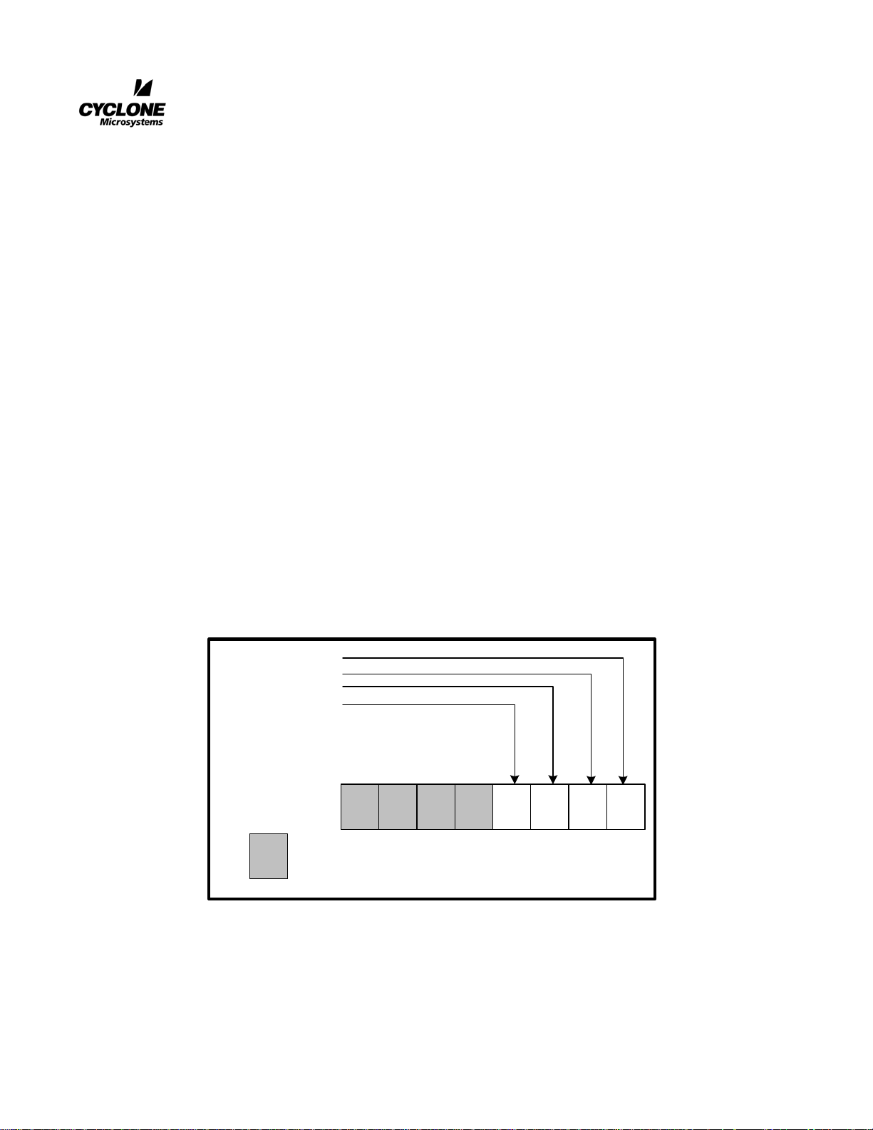
The CPCI-824 front panel has four green LEDs. The four green LEDs labeled IOP, ACT, STAT0, and
STAT1 are under software control. The LEDs are controlled by a write-only register which is located at
address E000 0001H. The LED Register bitmap is shown in Figure 2-2. A given LED is turned ON by
writing a “1” to the appropriate bit in the LED register.
Figure 2-2. LED Register Bitmap, E800 0001H
STAT0
Activity
IOP
STA1
(write only)
(1) LED on
(0) LED off
01324567
Reserved
2.8.3 User LEDs During Initialization
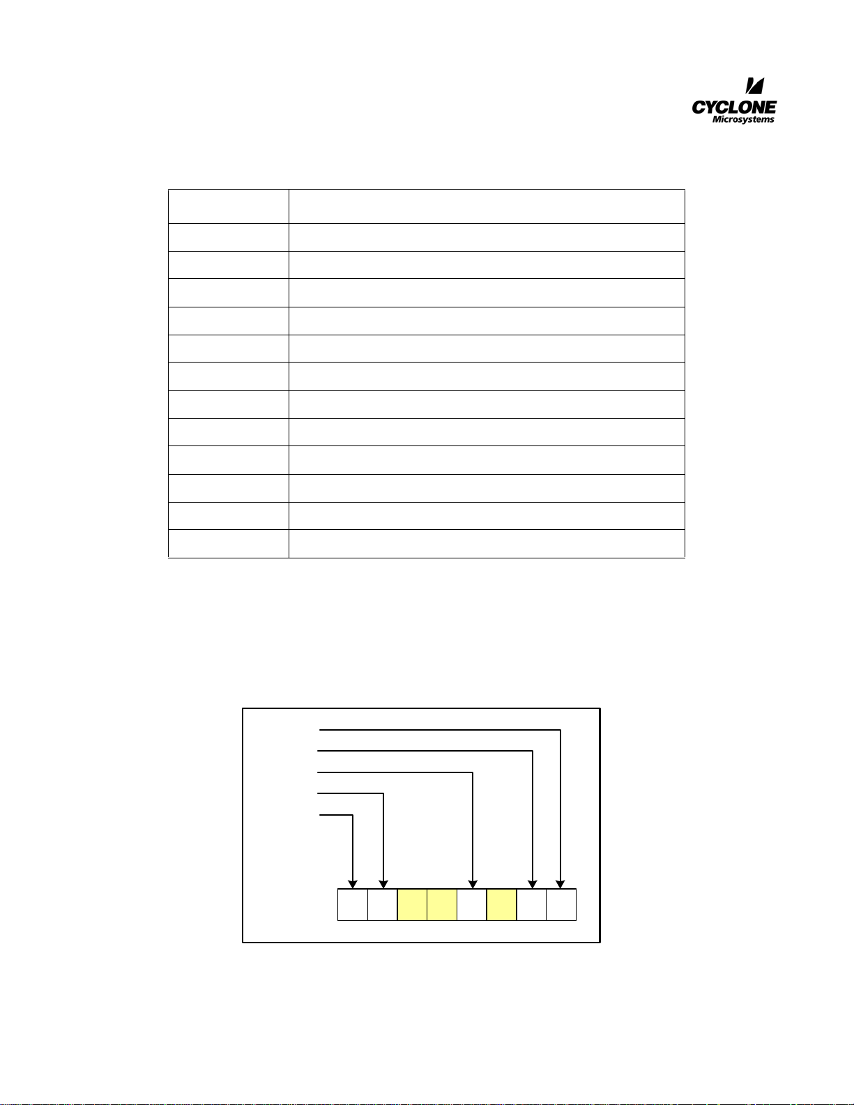
Breeze indicates the progress of its hardware initialization on the user LEDS. In the event that initialization should fail for some reason, the number of lit LEDs can be used to determine the cause of
failure. Table 2-6 lists the tests that correspond to each LED.
CPCI-824 User’s Manual 2-7
Revision 1.0, January 2006
Page 18
HARDWARE
Table 2-6. Breeze Start-up LEDS
LED TESTS
ACT TLBs set. External bus controller set
ST0 PCB arbitration priorities set
ST1 Interrupt controller set
IOP UART set
ACT, ST0 System reset check done.
ACT, ST1 I2C bus set. (first pass)
ACT, IOP Board configuration initialized
ST0, ST1 Board strapping validated
ST0, IOP I2C bus set. (second pass)
ST1, IP SDRAM initialized
ACT, ST0, ST1 SDRAM checked and cleared.
None Breeze entry
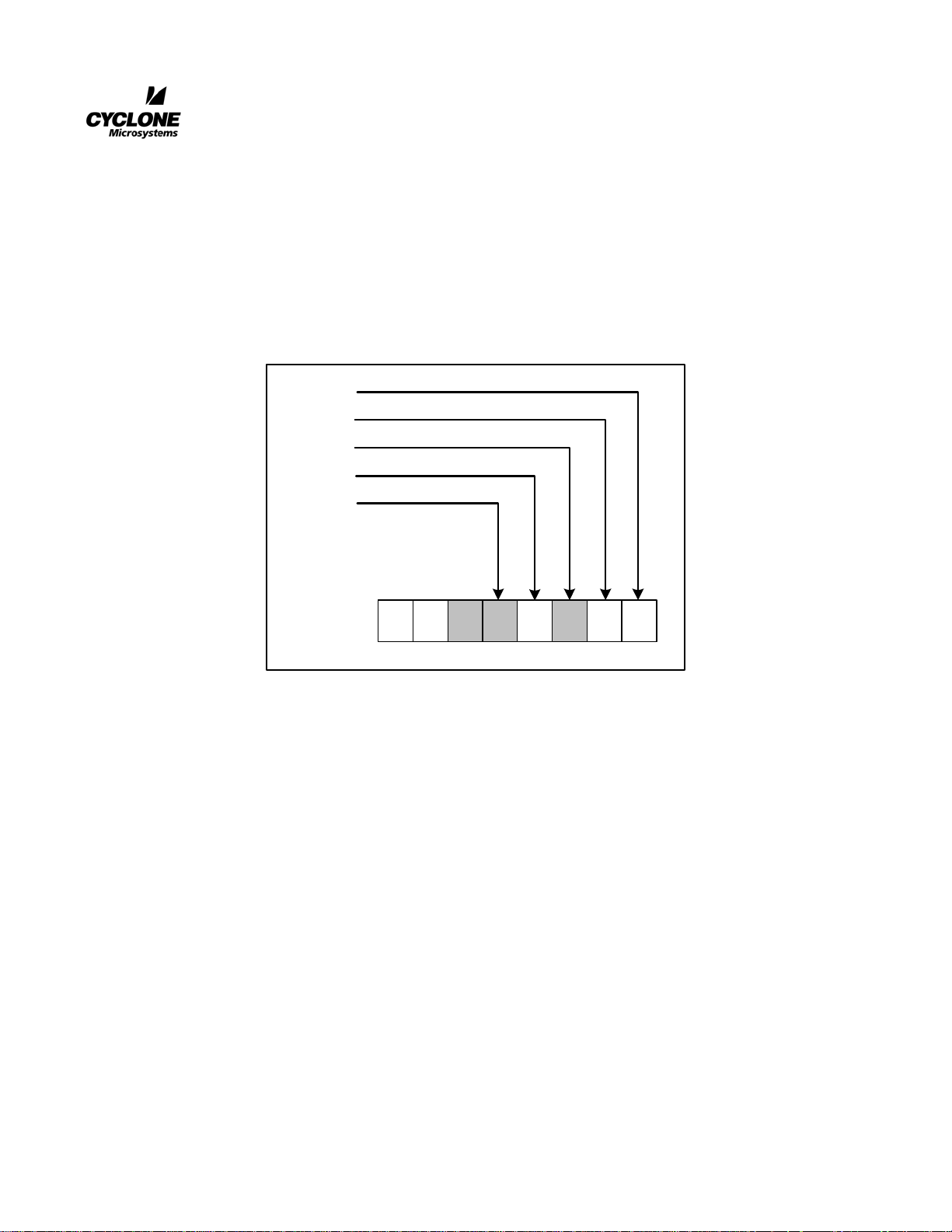
2.8.4 Geographic Addressing
CompactPCI backplanes that support 64-bit connector pin assignments are required to provide a unique
differentiation based upon which physical slot the board has been inserted. The CPCI-824 makes this
definition available to the software. The definition for GA[4:0] is shown in Figure 2.3.
Figure 2-3. Geographic Addressing Register, E800 0001h
GA0
GA1
GA2
GA3
GA4
READ Only
(1) +5V
(0) GND
2-8
7645 3210
CPCI-824 User’s Manual
Revision 1.0, January 2006
Page 19
2.8.5 Power Supply Monitoring
Two circuits are provided for monitoring the health of power supplies. Additional inputs to the
CompactPCI connector define pins for degraded, failed and detected power supplies. The definitions
for the CompactPCI connector J2 is provided in Appendix B. A failed or degraded power supply, as
long as it is detected, will cause an interrupt to the processor. Additionally, the state of the power
supply as defined by POWERGOOD, i.e. the power supply is neither degraded or failed, is displayed in
a green LED. Figure 2-4 shows the bit definition for the power supply status register.
Figure 2-4. Power Supply Status Register, E800 0000H
PS0 Failed
PS1 Failed
PS0 Detected
PS1 Detected
Degraded
HARDWARE
2.9 FAN MONITORING
Two circuits are provided for moni toring of the two fan frequ ency inputs. As in the case of the power
supply monitoring signals, additional inputs to J2 have been defined for the two fan inputs. Refer to
Appendix B for their pin locations. The fan monitoring circuits will provide an interrupt to the
processor if the frequency of the fan output falls below approximately 8K RPM. Green LEDs are
provided for fan interrupt status. If a fan frequency input causes an interrupt, the corresponding LED is
turned off.
2.10 I
2
C BUS
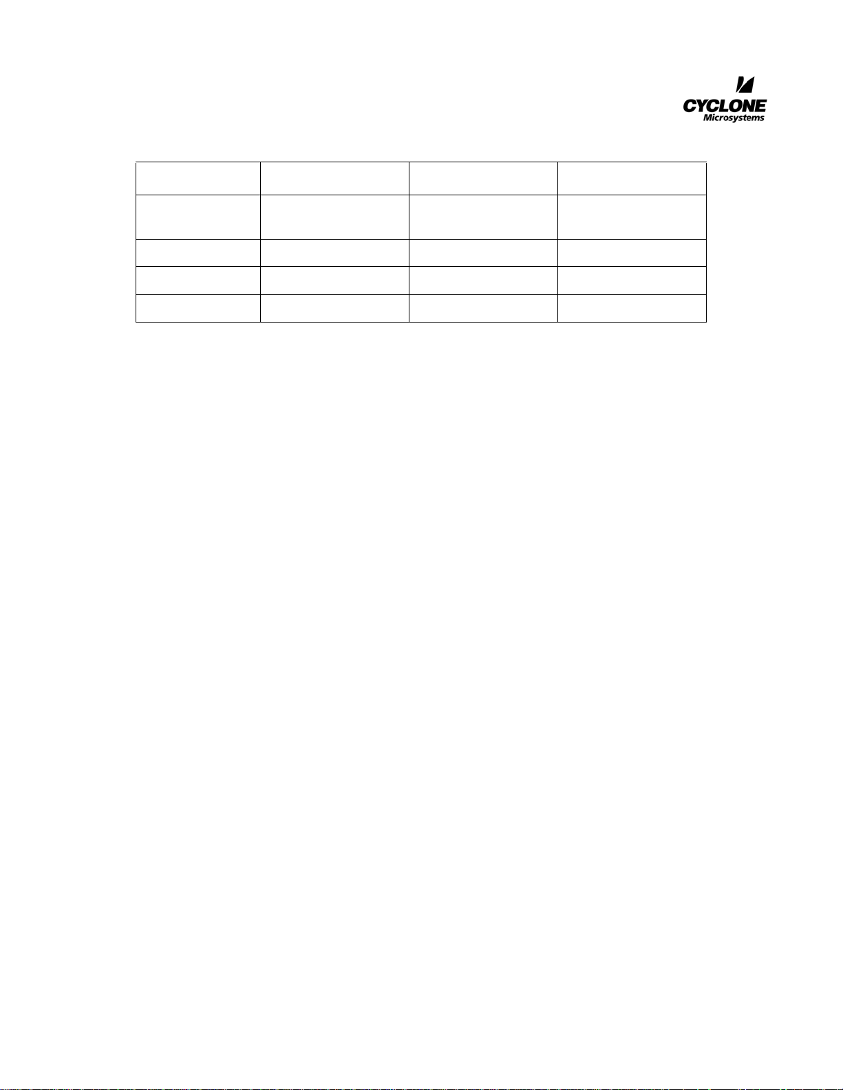
The CPCI-824 has five components attached to the Inter-Integrated Circuit (I
PPC440GP processor: the DDR SDRAM EEPROM, the two temperature sensors, the reset configuration Serial EEPROM, and the DDR SDRAM phase lock loop clock driver. The I
devices are shown in Table 2-7.
01324567
2
C) bus interface #0 of the
2
C addresses of the
CPCI-824 User’s Manual 2-9
Revision 1.0, January 2006
Page 20
HARDWARE
Designator Device Function Address
Table 2-7. I2C Device Addresses
J10
DDR SDRAM
EEPROM SODIMM
U13 LM75 Temp er ature Sensor 1001000x
U1 LM75 Temperature Sensor 1001001x
U16 24C08-LV Serial EEPROM 1010000x
2.10.1 SDRAM EEPROM
The EEPROM located on the DDR SDRAM module contains identification and configuration information. Breeze code will read this information on power-up and will properly configure the
PPC440GX processor to the SDRAM type. No user intervention is required.
2.10.2 Temperature Sensors
The LM75 temperature sensors have overtemperature trip points that will trigger an interrupt when
crossed. The sensors have been placed on the board U1 & U14 and share an interrupt line to the
processor. Polling the two devices will be required to determine which part has triggered the interrupt.
The sensors are placed in interrupt mode by the Breeze initialization code. The default overtemperature
point is 80 degrees Celsius. The sensors can be read for a temperature reading at any time, reading after
an interrupt clears the interrupt. The sensor will not interrupt again until the temperature h as dropped
below the hysteresis value (default is 75 degrees Celsius) and risen again passed the trip point. Consult
the LM75 data sheet for more details on programming the temperature sensors.
Memory
Configuration
10100011
2.10.3 Serial EEPROM
The first time a CPCI-820 is powered up, initial conditions are read from a serial EEPROM connected
to the I2C bus. The device is read during reset. Initially, the serial EEPROM is disabled and the
processor powers up in a default state. Once the board is programmed and the serial EEPROM is
programmed, then subsequent power ups will use the data stored.
2.10.4 Phase Lock Loop Clock Driver
The PPC440GX memory controller generates a single differential pair memory clock for the DDR
SDRAM devices. The CDCV850 is a low skew, low jitter, zero delay buffer that distributes the differential clock to the three input pairs of the 200 pin SoDIMM.
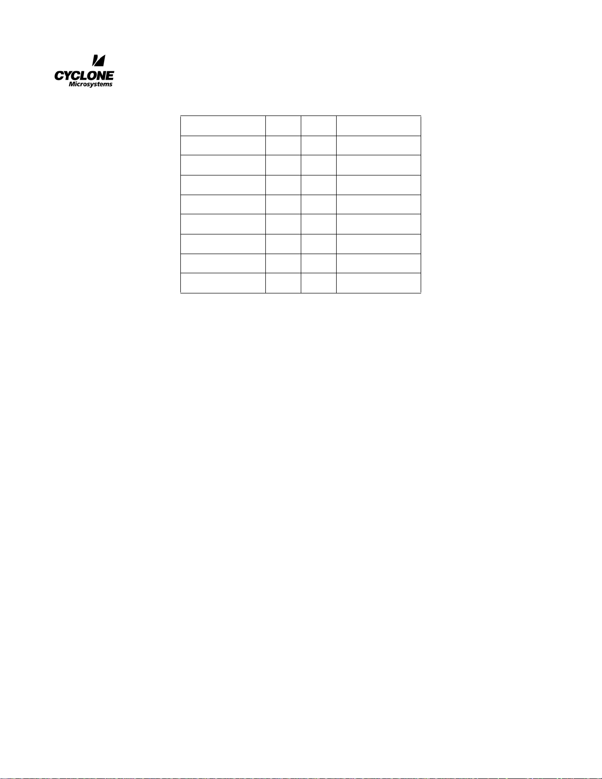
2.11 JTAG EMULATOR SUPPORT
The CPCI-824 provides a joint test action group JTAG emulator interface at J27 for XScale compatible
emulators. The JTAG emulator interface connects to the JTAG port of the IOP331 processor and has the
ability to assert a reset to the secondary PCI bus. The JTAG emulator header definition is shown in
Ta bl e 2-8
2-10
CPCI-824 User’s Manual
Revision 1.0, January 2006
Page 21
HARDWARE
Table 2-8. JTAG Emulator Pin Assignment
Signal Pin Pin Signal
TDO 1 2 No Connect
TDI 3 4 TRST#
NO Connect 5 6 VREF
TCK 7 8 No Connect
TMS 9 10 No Connect
SYS_HALT# 11 12 No Connect
No Connect 11 12 No Connect
No Connect 15 16 GND
CPCI-824 User’s Manual 2-11
Revision 1.0, January 2006
Page 22

A.1 INTRODUCTION
The PMC Module Interface allows PCI devices to be connected to the Local PCI interface of the CPCI824 host. The IEEE STD P1386.1, PCI Mezzanine Card (PMC), provides for one set of clocking and
arbitration signals per PMC Module. Cyclone Microsystems has expanded this to two sets per PMC
Module on the CPCI-824. With ability to connect a PMC module on the CPCI-824, up to two devices
are supported. Otherwise, with a few exceptions, the standard signals defined for 64-bit CPCI
connectors are used for the PMC Modules. The exceptions are noted in Section A.3. The timing for
devices on PMC Modules is the same as the timing for any other PCI device; see the PCI Local Bus
Specification revision 2.2 for details. The CPCI-824 PMC module location is defined as +3.3V
signalling. Note that only +3.3V or universal signalling PMC modules may be used on the CPCI-824.
A number of PMC Modules are available from Cyclone Microsystems. This section is intended for
users interested in developing their own modules.
A.2 PHYSICAL ATTRIBUTES
Please refer to IEEE P1386/Draft 2.0 for the physical dimensions of PMC modules.
APPENDIX A
PMC MODULE INTERFACE
A.3 PMC MODULE SIGNAL DEFINITIONS
PMC Modules use the signals defined in the IEEE STD P1386.1. The following four signals are added
to this definition to handle the expansion from one to two devices per PMC module:
• GNT1#
•REQ1#
•CLK1
• IDSEL1
Please note that the added signals used the PMC-RSVD signals as defined in IEEE STD P1386.1. The
PCI-RSVD remain untouched.
Also, note that GNT1# follows the description for GNT#, REQ1# follows th e description for REQ#,
CLK1 follows the description for CLK, and IDSEL1 follows the description for IDSEL. When the
appropriate signals are connected to PCI devices on a PMC Module, each device has the full
complement of PCI signals defined in the specification.
IDSEL signals are not provided. The designer of a PMC Module should connect the proper AD signal to
a device’s IDSEL pin. AD21:16 may be used depending on the desired number mapping scheme. The
suggested signal connections are shown in tables A-1 and A-2.
CPCI-824 User’s Manual A-1
Revision 1.0, January 2006
Page 23
PMC MODULE INTERFACE
Table A-1. PMC Clock & Arbitration Assignment
MODULE IDSEL ADDR IDSEL# CLOCK ARBITRATION
PMC 0 IDSEL# AD17 J12.25 CLKA REQ0#,GNT0#
PMC 0 IDSEL1# AD18 J12.34 CLKB REQ1#,GNT1#
Table A-2. PMC Interrupt Assignment
DEVICE INTx# 1
INTA# INTA# INTB#
INTB# INTB# INTC#
INTC# INTC# INTD#
INTD# INTD# INTA#
A.4 PMC MODULE CONNECTOR
PMC Modules use three board-to-board connectors (plug) with 64 pins each. The receptacles (i.e. AMP
P/N 120521-2) are located on the host platform and attach to the plugs (i.e. AMP P/N 1205 27-2). This
connector combination allows for a 10 mm board-to-board spacing. See IEEE P1386/Draft 2.0 for
dimensions and component clearance details.
ST
DEVICE 2ND DEVICE
A-2
CPCI-824 User’s Manual
Revision 1.0, January 2006
Page 24

PMC MODULE INTERFACE
Table A-3. P21 PMC Module Connector Pinout
Pin Signal Pin Signal
1TCK2-12V
3 GND 4 INTA#
5 INTB# 6 INTC#
7BUSMODE1#8 +5V
9 INTD# 10 PCI-RSVD
11 GND 12 PCI-RSVD
13 CLK 14 GND
15 GND 16 GNT#
17 REQ# 18 +5V
19 V(I/O) 20 AD31
21 AD28 22 AD27
23 AD25 24 GND
25 GND 26 C/BE3#
27 AD22 28 AD21
29 AD19 30 +5V
31 V(I/O) 32 AD17
33 FRAME# 34 GND
35 GND 36 IRDY#
37 DEVSEL# 38 +5V
39 GND 40 LOCK#
41 SDONE# 42 SBO#
43 PAR 44 GND
45 V(I/O) 46 AD15
47 AD12 48 AD11
49 AD09 50 +5V
51 GND 52 C/BE0#
53 AD06 54 AD05
55 AD04 56 GND
57 V(I/O) 58 AD03
59 AD02 60 AD01
61 AD00 62 +5V
63 GND 64 REQ64#
CPCI-824 User’s Manual A-3
Revision 1.0, January 2006
Page 25

PMC MODULE INTERFACE
Pin Signal Pin Signal
1 +12V 2 TRST#
3TMS4TDO
5 TDI 6 GND
7 GND 8 PCI-RSVD
9 PCI-RSVD 10 PCI-RSVD
11 BUSMODE2# 12 +3.3V
13 RST# 14 BUSMODE3#
15 +3.3V 16 BUSMODE4#
17 PCI-RSVD 18 GND
19 AD30 20 AD29
21 GND 22 AD26
23 AD24 24 +3.3V
25 IDSEL 26 AD23
27 +3.3V 28 AD20
29 AD18 30 GND
31 AD16 32 C/BE2#
33 GND 34 PMC+IDSEL1
35 TRDY# 36 +3.3V
37 GND 38 STOP#
39 PERR# 40 GND
41 +3.3V 42 SERR#
43 C/BE1# 44 GND
45 AD14 46 AD13
47 GND 48 AD10
49 AD08 50 +3.3V
51 AD07 52 PMC+REQ1
53 +3.3V 54 PMC+CLK1
55 PMC+GNT1# 56 GND
57 PMC-RSVD 58 PMC-RSVD
59 GND 60 PMC-RSVD
61 ACK64# 62 +3.3V
63 GND 64 PMC-RSVD
Table A-4. P22 PMC Module Connector Pinout
A-4
CPCI-824 User’s Manual
Revision 1.0, January 2006
Page 26

PMC MODULE INTERFACE
Table A-5. P23 PMC Module Connector Pinout
Pin Signal Pin Signal
1PCI-RSVD2 GND
3 GND 4 C/BE7#
5 C/BE6# 6 C/BE5#
7C/BE4#8 GND
9V(I/O)10PAR64
11 AD63 12 AD62
13 AD61 14 GND
15 GND 16 AD60
17 AD59 18 AD58
19 AD57 20 GND
21 V(I/O) 22 AD56
23 AD55 24 AD54
25 AD55 26 GND
27 GND 28 AD52
29 AD51 30 AD50
31 AD49 32 GND
33 GND 34 AD48
35 AD47 36 AD46
37 AD45 38 GND
39 V(I/O) 40 AD44
41 AD43 42 AD42
43 AD41 44 GND
45 GND 46 AD40
47 AD39 48 AD38
49 AD37 50 GND
51 GND 52 AD36
53 AD35 54 AD34
55 AD33 56 GND
57 V(I/O) 58 AD32
59 PCI-RSVD 60 PCI-RSVD
61 PCI-RSVD 62 GND
63 GND 64 PCI-RSVD
CPCI-824 User’s Manual A-5
Revision 1.0, January 2006
Page 27
B.1 INTRODUCTION
The CPCI-824 utilizes some of the reserved pins in J2 for Fan and Power Supply status informat ion.
Differences from the CPCI specification are shown in table B-1.
Pin C D E
20 FAL1# GND DET0#
21 FAN1 FAN0 DET1#
APPENDIX B
CPCI J2 DEFINITION
Table B-1. CPCI-824 J2 Definition
CPCI-824 User’s Manual B-1
Revision 1.0, January 2006
 Loading...