CyberOptics 003 Users Manual

CyberOptics
Semiconductor
WaferSense
AGS User’s
Guide
™

General
Information
WaferSense Gapping Wafer and Link
Changes or modifications not expressly approved by CyberOptics Semiconductor, Inc., may
void your authority to operate the WaferSense AGS.
The radio contained in the WaferSense AGS meets all the applicable FCC requirements for RF
Safety. While in operation, the FCC requires users and nearby persons to maintain a minimum
separation distance of 20 cm (8 inches) or farther from the WaferSense AGS.
The WaferSense Gapping Wafer and Link have been tested and found to comply with the
limits for a Class B digital device, pursuant to Part 15 of the FCC Rules. These limits are
designed to provide reasonable protection against harmful interference in a residential
installation. This equipment generates, uses and can radiate radio frequency energy and, if not
installed and used in accordance with the instructions, may cause harmful interference to radio
communications. However, there is no guarantee that interference will not occur in a particular
installation. If this equipment does cause harmful interference to radio or television reception,
which can be determined by turning the equipment off and on, the user is encouraged to try to
correct the interference by one or more of the following measures:
• Reorient or relocate the receiving antenna.
• Increase the separation between the equipment and receiver.
• Connect the equipment into an outlet on a circuit different from that to which the
receiver is connected.
• Consult the dealer or an experienced radio/TV technician for help.
This device complies with part 15 of the FCC Rules. Operation is subject to the following two conditions: (1)
This device may not cause harmful interference, and (2) this device must accept any interference received, including
interference that may cause undesired operation.
This ISM device complies with Canadian ICES-001.
Cet appareil ISM est conforme à la norme NMB-001 du Canada.
Caution
Electrostatic discharge (ESD) can damage the AGS. Handle the AGS in an ESD-safe
area. If such an area is not available, wear an antistatic wrist strap or touch a grounded
surface before handling the AGS.
ii

WaferSense Technical Support
Technical support is available from CyberOptics Semiconductor Monday through Friday,
8:00 A.M. to 5:00 P.M. Pacific Time.
E-mail: CSsupport@cyberoptics.com
Phone: +1 503 495-2200
800-366-9131 (US and Canada only)
Fax: +1 503 495-2201
WaferSense and GapView are trademarks of CyberOptics Semiconductor, Inc.
Third-party brands and names are the property of their respective owners.
Copyright © 2006-2008, CyberOptics Semiconductor, Inc. All rights reserved.
CyberOptics Semiconductor, Inc.
13555 S.W. Millikan Way
Beaverton, OR 97005
P/N 920-0701-02
iii

Table of
Contents
General Information ......................................................ii
Chapter 1
Introduction....................................................................................1.1
Chapter 2
Installing Your AGS....................................................................... 2.1
Installing the Software....................................................................2.1
Installing the Wireless Link............................................................2.3
Checking Communications Between the Link and the Wafer ......2.5
Registering Your Gapping Wafer for Calibration Service..............2.6
Running the GapView Application ................................................2.7
Technical Support ..........................................................................2.9
Chapter 3
Using Your AGS............................................................................. 3.1
Opening and Closing the Clean Box..............................................3.2
Using the AGS Gapping Wafer Buttons and Status Lights ...........3.3
Performing a Basic Gap Measurement ..........................................3.4
Setting the Gap Criteria ..................................................................3.9
Applying Offsets to the Gap Readings......................................... 3.10
Setting the Wafer Display Orientation .........................................3.12
Logging Your Readings ...............................................................3.13
Logging a Reading..................................................................................3.13
Including User-Specified Information in the Log File .....................3.14
Changing the Log File............................................................................3.15
Displaying Readings from a Log File ..................................................3.15
Printing the GapView Window..................................................... 3.16
Monitoring the Operating Temperature ...................................... 3.17
iv

Table of Contents
Using the Rechargeable Battery................................................... 3.18
Monitoring the Battery Level................................................................3.18
Charging the Battery ..............................................................................3.18
Monitoring the Wireless Connection to the Gapping Wafer ....... 3.19
Changing the Pairing Between the Gapping Wafer and Link .....3.20
Saving Your Settings..................................................................... 3.21
Loading Settings from a File.................................................................3.21
Chapter 4
Maintaining Your AGS .................................................................. 4.1
Annual Factory Calibration and Battery Replacement ..................4.2
Battery Use and Disposal ...............................................................4.2
Field Calibrating Your AGS............................................................4.3
Chapter 5
Specifications................................................................................. 5.1
System Requirements .....................................................................5.1
AGS Hardware ................................................................................5.1
Environmental ..........................................................................................5.1
Power..........................................................................................................5.1
Range and Accuracy.................................................................................5.1
Index.....................................................................Index.1
v

List of
Illustrations
Chapter 2
Figure 2.1: The InstallShield Wizard.......................................................2.2
Figure 2.2: Found New Hardware Wizard..............................................2.3
Figure 2.3: Installing the Wireless Link Device......................................2.4
Figure 2.4: Starting the GapView Application ........................................2.7
Figure 2.5: Calibration Registration Dialog............................................2.8
Figure 2.6: The About GapView Dialog..................................................2.9
Figure 2.7: The About your AGS Wafer Dialog ......................................2.9
Chapter 3
Figure 3.1: Opening the Clean Box.........................................................3.2
Figure 3.2: Gap Measurements ...............................................................3.4
Figure 3.3: The GapView Application.....................................................3.5
Figure 3.4: Aligning the Gapping Wafer .................................................3.6
Figure 3.5: Numeric Readouts................................................................3.7
Figure 3.6: Graphical Readouts...............................................................3.8
Figure 3.7: Set Gap Criteria Dialog .........................................................3.9
Figure 3.8: Set Gap Offsets Dialog........................................................ 3.10
Figure 3.9: Applying the Gap Offset ..................................................... 3.11
Figure 3.10: Wafer Orientation in GapView.......................................... 3.12
Figure 3.11: Logging a Reading ............................................................3.14
Figure 3.12: Set Station Information dialog ..........................................3.15
Figure 3.13: Temperature Monitoring Gauge ....................................... 3.17
Figure 3.14: Battery Monitor .................................................................3.18
Figure 3.15: Wireless Connection Monitor............................................3.20
Chapter 4
Figure 4.1: Wafer Calibration Status Dialog............................................4.2
Figure 4.2: Field Calibrate Button and Last Calibration ........................4.3
Figure 4.3: Step 1 of 3 Start Calibration Dialog.......................................4.4
Figure 4.4: Step 2 of 3 Place AGS Wafer Dialog......................................4.4
Figure 4.5: Step 3 of 3 Finish Calibration Dialog....................................4.5
vi

Chapter 1
Introduction
The CyberOptics Semiconductor WaferSense™ Automatic Gapping System (AGS) measures
gaps that are critical to the outcome of semiconductor processes such as thin-film deposition,
sputtering, and etch. It uses a capacitive sensing technique (patent pending) that consists of
three sensors and responds to the proximity of a conductive electrode, such as a shower head,
to return live gap measurements that display on your laptop or PC in numerical and graphical
form. The GapView™ software application makes it easy to precisely adjust equipment. The
large display and wireless link let you place the computer at a convenient distance from the
AGS gapping wafer.
AGS consists of the following components:
• Gapping wafer. The gapping wafer is designed with a wafer-like form factor, so it
can fit in most wafer-handling equipment. The gapping wafer package is also vacuum
compatible.
• GapView software. The GapView software application monitors the gapping wafer
and displays gap measurements and other status information in real time. GapView
runs on most personal computers that use the Microsoft Windows operating system.
• Wireless link. The GapView software communicates with the gapping wafer by
using a Bluetooth wireless link that attaches to a USB port on a personal computer.
• Clean box. The clean box lets you store the wafer when not in use.
• Battery charger and adapter cable. The battery charger and adapter cable let you
recharge the gapping wafer’s battery.
• Carrying case. The carrying case makes it easy to take your complete AGS system
with you in the plant or on the road.
The following chapter gives you instructions for installing your AGS system.
1.1

Chapter 2
Installing Your AGS
This chapter describes the procedures you need to perform to install your AGS and get it ready
for use. For best results, perform the procedures in the order they are presented in this chapter:
1. Installing the software
2. Installing the wireless link on the USB port
3. Checking communications between the link and the gapping wafer
4. Registering your gapping wafer
5. Running the GapView application
Caution
Dropping the gapping wafer or hitting it against a hard object can bend, break, or chip the
housing; damage the internal components; or knock the gapping wafer out of calibration.
While it is not as fragile as an actual silicon wafer, handle the gapping wafer with care, as
you would any precision instrument. If the gapping wafer is damaged or in need of
calibration, see Chapter 4, “Maintaining Your AGS.”
Installing the Software
To run the WaferSense AGS software, your computer must have the following:
• Windows 2000, Windows XP, or Windows Vista operating system
• One free high-power USB 1.1 or USB 2.0 port
To install the WaferSense AGS software:
1. Log on using an account with Administrator privileges.
2.1
Chapter 2. Installing Your AGS
2. Insert the WaferSense AGS Installation Disk into the CD drive.
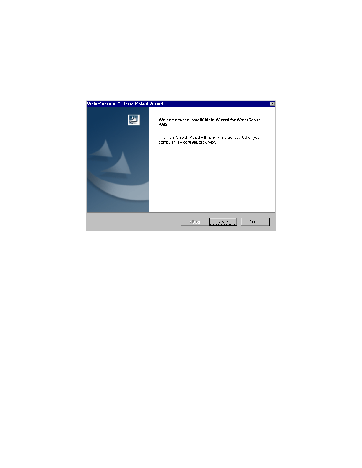
The InstallShield Wizard starts automatically, as shown in Figure 2.1. If the wizard doesn’t
start automatically, use Windows Explorer to view the contents of the CD and doubleclick the setup.exe program.
Figure 2.1: The InstallShield Wizard
3. Follow the instructions provided by the wizard to install the software.
4. After you complete the instructions for all of the wizard screens, click Finish. If
Windows notifies you that the drivers have not passed Windows logo testing, just click
Continue Anyway to complete the installation.
By default, the Setup program installs the GapView application in a new program group called
WaferSense AGS. Setup also installs an online copy of this user’s guide, which is available from
the GapView Help menu and in the WaferSense AGS program group in the Windows
Start menu.
2.2
Chapter 2. Installing Your AGS
Installing the Wireless Link
To install the wireless link:
1. Turn on your computer.
2. Locate an unused, high-power USB port on your computer. The AGS wireless link
module requires a high-power USB port, such as the built-in ports on your computer and
ports on USB hubs that have power cords. Unpowered USB hubs won’t work.
3. The USB cable provided with your AGS has a different plug on each end. Locate the end
with the plug that matches the USB port on your computer and plug the cable into
the port.
4. Plug the other end of the cable into the link module.
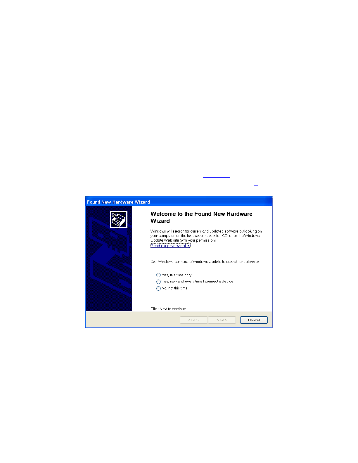
The Windows operating system recognizes the new link module hardware and displays
the Found New Hardware Wizard, as shown in Figure 2.2. If the wizard your system
displays doesn’t offer to check with Windows Update, skip to step 6.
Figure 2.2: Found New Hardware Wizard
5. Choose No, not this time and click Next.
2.3
Chapter 2. Installing Your AGS
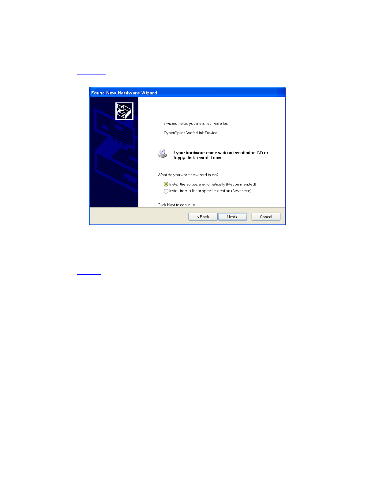
The wizard offers to help you install software for the WaferSense link, as shown in
Figure 2.3.
Figure 2.3: Installing the Wireless Link Device
6. Choose Install the software automatically and click Next.
If you already installed the WaferSense AGS software (see “Installing the Software,” on
page 2.1), Windows will automatically find the drivers. If not, the drivers are located in the
Utilities folder on the installation CD-ROM.
7. After you complete the instructions for all of the wizard screens, click Finish.
The Power light on the module turns on indicating that the module is getting power from
the USB port. Ignore the Pair Status and Connection Status lights for now.
2.4

Chapter 2. Installing Your AGS
Checking Communications Between the Link and the Wafer
To complete the installation, verify that the gapping wafer and link can communicate as
follows:
1. The gapping wafer operates from an internal rechargeable battery. Before using the
gapping wafer for the first time, charge it for two hours. For information on checking the
charge on the battery and the procedure for recharging, see “Using the Rechargeable
Battery,” on page 3.18.
2. Unplug the battery charger, open the clean box (see “Opening and Closing the Clean
Box,” on page 3.2), and remove the wafer from the box.
3. Press the ON / OFF button to turn on the gapping wafer.
The Power light on the gapping wafer turns on.
4. Verify that the Pair Status lights on both the gapping wafer and link module are on. If
either light is not on, your gapping wafer and link might not be paired with each other. To
reset the pairing, see “Changing the Pairing Between the Gapping Wafer and Link,” on
page 3.20.
5. Immediately after turning on the gapping wafer, the Connection Status lights on the
gapping wafer and link will blink slowly. After a few seconds the gapping wafer and link
will connect and both lights will be on and no longer blinking. If the lights continue to
blink, see “Monitoring the Wireless Connection to the Gapping Wafer,” on page 3.19.
6. After starting the GapView application (see “Running the GapView Application,” on
page 2.7), you can verify the connection to the gapping wafer by comparing the serial
number printed on the gapping wafer to the serial number shown in the About your AGS
Wafer dialog, which is available in the GapView application by choosing the Help >
About your AGS Wafer menu item. If the GapView application isn’t running, the AGS
wafer turns off automatically after 30 minutes.
That completes the installation of your AGS.
2.5

Chapter 2. Installing Your AGS
Registering Your Gapping Wafer for Calibration Service
To maintain optimum performance, every twelve months you should have your gapping wafer
calibrated and the battery replaced. These services can be performed only at the factory.
To help you keep track of the next service date so you can schedule this service when it is
convenient, register your WaferSense AGS gapping wafer with the factory. When you start the
GapView application (see “Running the GapView Application,” on page 2.7), it prompts you to
register your gapping wafer for calibration. You can also register your gapping wafer in any of
the following ways:
• On the Internet: http://www.cyberopticssemi.com/ws_register.html
• By phone: 800-366-9131 (US and Canada only)
• By faxing the WaferSense AGS Calibration Registration to: +1 503 495-2201
• By sending an e-mail message containing the information specified on the WaferS ense
AGS Calibration Registration to: register@cyberoptics.com.
2.6
Chapter 2. Installing Your AGS
Running the GapView Application
To start the GapView application:
1. From the Windows Start > All Programs menu, choose WaferSense AGS > GapView.
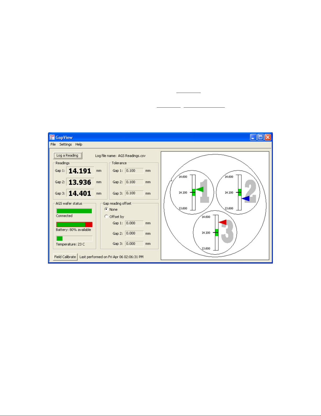
The GapView application starts, as shown in Figure 2.4. Initializing communications
between the gaping wafer and GapView usually takes less than one second. For
information on using GapView, see “Chapter 3, Using Your AGS.” If you haven’t
registered your gapping wafer, GapView also displays the Calibration Registration dialog.
To complete the registration, proceed to the next step.
Figure 2.4: Starting the GapView Application
2.7

Chapter 2. Installing Your AGS
2. If GapView displays the WaferSense AGS Calibration Registration dialog, as shown in
Figure 2.5, you haven’t registered your gapping wafer. Follow the instructions in the
dialog to complete the registration.
Figure 2.5: Calibration Registration Dialog
2.8
 Loading...