

CTLST CAT25C33U14A-1.8TE13, CAT25C33U14-TE13, CAT25C33U14-1.8TE13, CAT25C33U-TE13, CAT25C33U-1.8TE13 Datasheet
...
1
CAT25C03/05/09/17/33
2K/4K/8K/16K/32K SPI Serial CMOS E2PROM
FEATURES
■ 10 MHz SPI Compatible
■ 1.8 to 6.0 Volt Operation
■ Hardware and Software Protection
■ Zero Standby Current
■ Low Power CMOS Technology
■ SPI Modes (0,0 &1,1)
■ Commercial, Industrial and Automotive
Temperature Ranges
■ 1,000,000 Program/Erase Cycles
■ 100 Year Data Retention
■ Self-Timed Write Cycle
■ 8-Pin DIP/SOIC, 16-Pin SOIC and 14-Pin TSSOP
■ Page Write Buffer
■ Write Protection
– Protect First Page, Last Page, Any 1/4 Array
or Lower 1/2 Array
PIN CONFIGURATION
DIP Package (P)SOIC Package (S16)
PIN FUNCTIONS
Pin Name Function
SO Serial Data Output
SCK Serial Clock
WP Write Protect
V
CC
+1.8V to +6.0V Power Supply
V
SS
Ground
CS Chip Select
SI Serial Data Input
HOLD Suspends Serial Input
NC No Connect
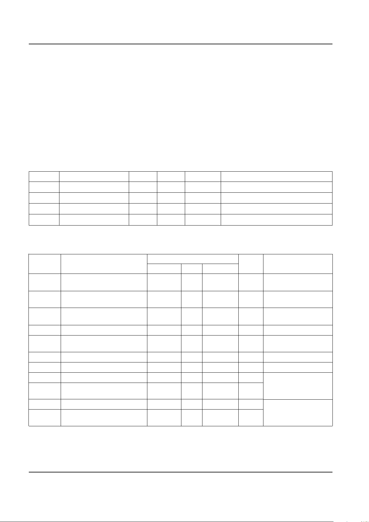
BLOCK DIAGRAM
© 1998 by Catalyst Semiconductor, Inc.
Characteristics subject to change without notice
Advanced
DESCRIPTION
The CAT25C03/05/09/17/33 is a 2K/4K/8K/16K/32K-Bit
SPI Serial CMOS E2PROM internally organized as
256x8/512x8/1024x8/2048x8/4096x8 bits. Catalyst’s
advanced CMOS Technology substantially reduces device power requirements. The CAT25C03/05 features a
16-byte page write buffer. The 25C09/17/33 features a
32-byte page write buffer.The device operates via the
SPI bus serial interface and is enabled though a Chip
Select (CS). In addition to the Chip Select, the clock
input (SCK), data in (SI) and data out (SO) are required
to access the device. The HOLD pin may be used to
suspend any serial communication without resetting the
serial sequence. The CAT25C03/05/09/17/33 is designed with software and hardware write protection
features. The device is available in 8-pin DIP, 8-pin
SOIC, 16-pin SOIC, 8-pin TSSOP and 14-pin TSSOP
packages.
TSSOP Package (U14)
SENSE AMPS
SHIFT REGISTERS
SPI
CONTROL
LOGIC
WORD ADDRESS
BUFFERS
I/O
CONTROL
E2PROM
ARRAY
COLUMN
DECODERS
XDEC
HIGH VOL T A GE/
TIMING CONTROL
SO
25C128 F02
STATUS
REGISTER
BLOCK
PROTECT
LOGIC
CONTROL LOGIC
DATA IN
STORAGE
SI
CS
WP
HOLD
SCK
SOIC Package (S)
V
SS
SO
WP
V
CC
HOLD
SCK
SI
1
2
3
4
8
7
6
5
CS
SO
WP
CS
V
CC
SCK
SI
1
2
3
4
8
7
6
5
V
SS
HOLD
CS
NC
1
2
3414
13
12
11
NC
NC
NC
5
6
710
98
NC
SCK
V
SS
SI
NC
WP
VCC
HOLDSO
15
16
NCNC
CS
WP
HOLD
VCC
NC
NC
NC NC
SO
NC
NC
V
SS
SCK
SI
1
2
3
4
5
6
7
8
9
10
11
12
13
14
TSSOP Package (U)
8
7
6
5
V
CC
WP
SCL
CS
V
SS
1
2
3
4
SO
HOLD
SI
Doc. No. 25068-00 2/98
2
CAT25C03/05/09/17/33
Doc. No. 25068-00 2/98
Advanced
D.C. OPERATING CHARACTERISTICS
VCC = +1.8V to +6.0V, unless otherwise specified.
Limits
Symbol Parameter Min. Typ. Max. Units Test Conditions
I
CC1
Power Supply Current 5 mA VCC = 5V @ 5MHz
(Operating Write) SO=open; CS=Vss
I
CC2
Power Supply Current 0.4 mA VCC = 5.5V
(Operating Read) F
CLK
= 5MHz
I
SB
Power Supply Current 0 µA CS = V
CC
(Standby) VIN = VSS or V
CC
I
LI
Input Leakage Current 2 µA
I
LO
Output Leakage Current 3 µAV
OUT
= 0V to VCC,
CS = 0V
V
IL
(3)
Input Low Voltage -1 VCC x 0.3 V
V
IH
(3)
Input High Voltage VCC x 0.7 V
CC
+ 0.5 V
V
OL1
Output Low Voltage 0.4 V
V
OH1
Output High Voltage VCC - 0.8 V
V
OL2
Output Low Voltage 0.2 V 1.8V≤VCC<2.7V
V
OH2
Output High Voltage VCC-0.2 V IOL = 150µA
IOH = -100µA
ABSOLUTE MAXIMUM RATINGS*
Temperature Under Bias ................. –55°C to +125°C
Storage Temperature....................... –65°C to +150°C
Voltage on any Pin with
Respect to Ground
(1)
............ –2.0V to +VCC +2.0V
VCC with Respect to Ground ............... –2.0V to +7.0V
Package Power Dissipation
Capability (Ta = 25°C)................................... 1.0W
Lead Soldering Temperature (10 secs) ............ 300°C
Output Short Circuit Current
(2)
........................ 100 mA
*COMMENT
Stresses above those listed under “Absolute Maximum
Ratings” may cause permanent damage to the device.
These are stress ratings only, and functional operation
of the device at these or any other conditions outside of
those listed in the operational sections of this specification is not implied. Exposure to any absolute maximum
rating for extended periods may affect device performance and reliability.
RELIABILITY CHARACTERISTICS
Symbol Parameter Min. Max. Units Reference Test Method
N
END
(3)
Endurance 1,000,000 Cycles/Byte MIL-STD-883, Test Method 1033
T
DR
(3)
Data Retention 100 Years MIL-STD-883, Test Method 1008
V
ZAP
(3)
ESD Susceptibility 2000 Volts MIL-STD-883, Test Method 3015
I
LTH
(3)(4)
Latch-Up 100 mA JEDEC Standard 17
Note:
(1) The minimum DC input voltage is –0.5V. During transitions, inputs may undershoot to –2.0V for periods of less than 20 ns. Maximum DC
voltage on output pins is VCC +0.5V, which may overshoot to VCC +2.0V for periods of less than 20 ns.
(2) Output shorted for no more than one second. No more than one output shorted at a time.
(3) This parameter is tested initially and after a design or process change that affects the parameter.
(4) Latch-up protection is provided for stresses up to 100 mA on address and data pins from –1V to VCC +1V.
4.5V≤VCC<5.5V
IOL = 3.0mA
IOH = -1.6mA
3
CAT25C03/05/09/17/33
Doc. No. 25068-00 2/98
Advanced
Limits
1.8, 2.5 4.5V-5.5V Test
SYMBOL PARAMETER Min. Max. Min. Max. UNITS Conditions
t
SU
Data Setup Time 50 10 ns VIH = 2.4V
t
H
Data Hold Time 50 20 ns CL = 100pF
t
WH
SCK High Time 200 40 ns VOL = 0.8V
t
WL
SCK Low Time 200 40 ns VOH = 2.0v
f
SCK
Clock Frequency DC 2 DC 10 MHz
t
LZ
HOLD to Output Low Z 50 50 ns
t
RI
(1)
Input Rise Time 2 2 µs
t
FI
(1)
Input Fall Time 2 2 µs
t
HD
HOLD Setup Time 100 40 ns
t
CD
HOLD HOLD Time 100 40 ns CL = 100pF
t
WC
Write Cycle Time 10 5 ms
t
V
Output Valid from Clock Low 200 80 ns
t
HO
Output HOLD Time 0 0 ns
t
DIS
Output Disable Time 250 75 ns
t
HZ
HOLD to Output High Z 100 50 ns
t
CS
CS High Time 250 100 ns
t
CSS
CS Setup Time 250 100 ns
t
CSH
CS HOLD Time 250 100 ns
NOTE:
(1) This parameter is tested initially and after a design or process change that affects the parameter.
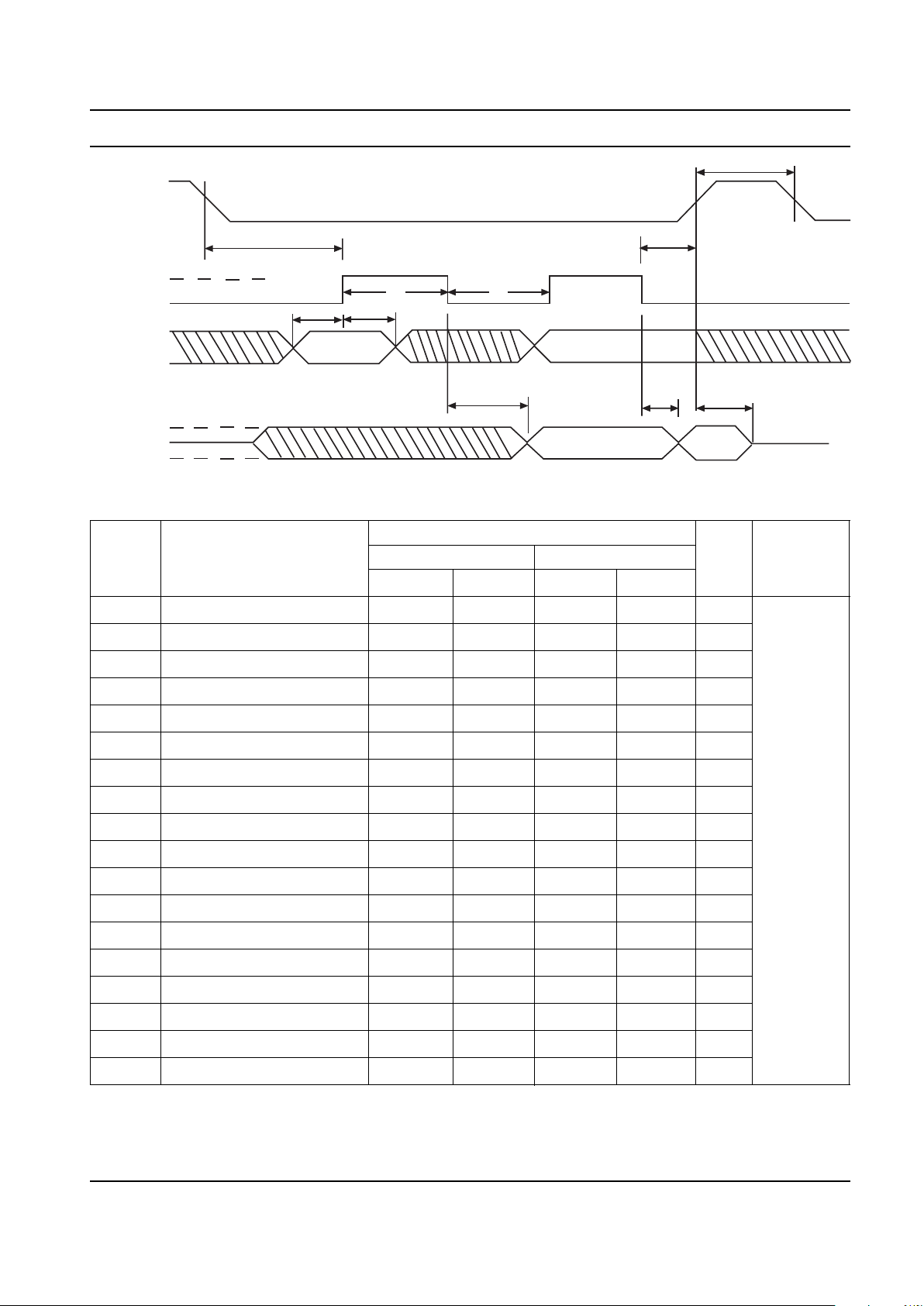
A.C. CHARACTERISTICS
Figure 1. Sychronous Data Timing
CL = 50pF
VALID IN
V
IH
V
IL
t
CSS
V
IH
V
IL
V
IH
V
IL
V
OH
V
OL
HI-Z
t
SU
t
H
t
WH
t
WL
t
V
t
CS
t
CSH
t
HO
t
DIS
HI-Z
CS
SCK
SI
SO
 Loading...