

CTLST CAT25C322U14-45TE13, CAT25C322U14-42TE13, CAT25C322U14-30TE13, CAT25C322U14-28TE13, CAT25C322U14-25TE13 Datasheet
...
9-95
CAT25CXXX
Supervisory Circuits with SPI Serial E2PROM, Precision Reset Controller and Watchdog Timer
FEATURES
■ 10 MHz SPI Compatible
■ 1.8 to 6.0 Volt Operation
■ Hardware and Software Protection
■ Zero Standby Current
■ Low Power CMOS Technology
■ SPI Modes (0,0 &1,1)
■ Commercial, Industrial and Automotive
Temperature Ranges
■ Active High or Low Reset Outputs
– Precision Power Supply Voltage Monitoring
– 5V, 3.3V, 3V and 1.8V Options
■ Watchdog Timer on
CSCS
CSCS
CS
■ 1,000,000 Program/Erase Cycles
■ 100 Year Data Retention
■ Self-Timed Write Cycle
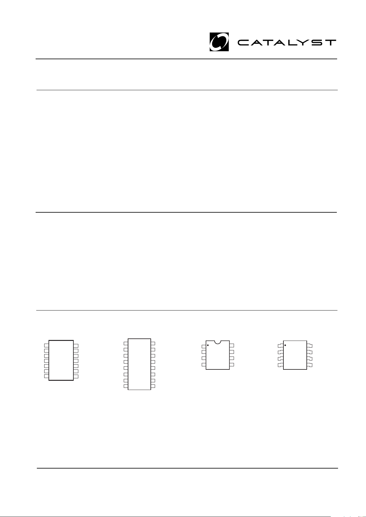
■ 8-Pin DIP/SOIC, 16-Pin SOIC and 14-Pin TSSOP
■ Page Write Buffer
■ Block Write Protection
– Protect 1/4, 1/2 or all of E2PROM Array
■ Programmable Watchdog Timer
■ Built-in inadvertent Write Protection
– VCC Lock Out
© 1998 by Catalyst Semiconductor, Inc.
Characteristics subject to change without notice
Advanced
DESCRIPTION
The CAT25CXXX is a single chip solution to three
popular functions of EEPROM Memory, precision reset
controller and watchdog timer. The EEPROM Memory is
a 2K/4K/8K/16K/32K-Bit SPI Serial CMOS E2PROM
internally organized as 256x8/512x8/1024x8/2048x8/
4096x8 bits. Catalyst’s advanced CMOS Technology
substantially reduces device power requirements. The
2K/4K devices feature a 16-byte page write buffer. The
8K/16K/32K devices feature a 32-byte page write
buffer.The device operates via the SPI bus serial interface and is enabled though a Chip Select (CS). In
addition to the Chip Select, the clock input (SCK), data
in (SI) and data out (SO) are required to access the
device. The reset function of the 25CXXX protects the
system during brown out and power up/down condtions.
During system failure the watchdog timer feature protects the microcontroller with a reset signal. The
CAT25CXXX is designed with software and hardware
write protection features including Block Lock protection. The device is available in 8-pin DIP, 8-pin SOIC, 16pin SOIC and 14-pin TSSOP packages.
CS
NC
1
2
3414
13
12
11
NC
NC
NC
5
6
710
98
NC
SCK
V
SS
SI
NC
WP
VCC
RESET/RESETSO
15
16
NCNC
PIN CONFIGURATION
DIP Package (P)
SOIC Package (S16)
TSSOP Package (U14)
SOIC Package (S)
V
SS
SO
WP
V
CC
RESET/RESE
T
SCK
SI
1
2
3
4
8
7
6
5
CS
CS
WP
RESET/RESET
VCC
NC
NC
NC NC
SO
NC
NC
V
SS
SCK
SI
1
2
3
4
5
6
7
8
9
10
11
12
13
14
SO
WP
CS
V
CC
SCK
SI
1
2
3
4
8
7
6
5
V
SS
RESET/RESET
9-96
CAT25CXXX
Stock No. 21085-01 4/98
Advanced
PIN FUNCTIONS
Pin Name Function
SO Serial Data Output
SCK Serial Clock
WP Write Protect
V
CC
+1.8V to +6.0V Power Supply
V
SS
Ground
CS Chip Select
SI Serial Data Input
RESET/RESET Reset I/O
NC No Connect
BLOCK DIAGRAM
RELIABILITY CHARACTERISTICS
Symbol Parameter Min. Max. Units Reference Test Method
N
END
(3)
Endurance 1,000,000 Cycles/Byte MIL-STD-883, Test Method 1033
T
DR
(3)
Data Retention 100 Years MIL-STD-883, Test Method 1008
V
ZAP
(3)
ESD Susceptibility 2000 Volts MIL-STD-883, Test Method 3015
I
LTH
(3)(4)
Latch-Up 100 mA JEDEC Standard 17
Power-Up Timing
(1)(2)
Symbol Parameter Max. Units
t
PUR
Power-up to Read Operation 1 ms
t
PUW
Power-up to Write Operation 1 ms
(1) This parameter is tested initially and after a design or process change that affects the parameter.
(2) t
PUR
and t
PUW
are the delays required from the time VCC is stable until the specified operation can be initiated.
(3) This parameter is tested initially and after a design or process change that affects the parameter.
(4) Latch-up protection is provided for stresses up to 100 mA on address and data pins from –1V to VCC +1V.
SENSE AMPS
SHIFT REGISTERS
SPI
CONTROL
LOGIC
WORD ADDRESS
BUFFERS
I/O
CONTROL
E2PROM
ARRAY
COLUMN
DECODERS
XDEC
HIGH VOL TAGE/
TIMING CONTROL
SO
25CXXX F02.1
STATUS
REGISTER
BLOCK
PROTECT
LOGIC
CONTROL LOGIC
DATA IN
STORAGE
SI
CS
WP
RESET/RESET
SCK
Reset Controller
Watchdog
High Precision
VCC Monitor
9-97
CAT25CXXX
Stock No. 21085-01 4/98
Advanced
D.C. OPERATING CHARACTERISTICS
VCC = +1.8V to +6.0V, unless otherwise specified.
Limits
Symbol Parameter Min. Typ. Max. Units Test Conditions
I
CC1
Power Supply Current 5 mA VCC = 5V @ 5MHz
(Operating Write) SO=open; CS=Vss
I
CC2
Power Supply Current 0.4 mA VCC = 5.5V
(Operating Read) F
CLK
= 5MHz
I
SB
Power Supply Current 0 µA CS = V
CC
(Standby) VIN = VSS or V
CC
I
LI
Input Leakage Current 2 µA
I
LO
Output Leakage Current 3 µAV
OUT
= 0V to VCC,
CS = 0V
V
IL
(3)
Input Low Voltage -1 VCC x 0.3 V
V
IH
(3)
Input High Voltage VCC x 0.7 V
CC
+ 0.5 V
V
OL1
Output Low Voltage 0.4 V
V
OH1
Output High Voltage VCC - 0.8 V
V
OL2
Output Low Voltage 0.2 V 1.8V≤VCC<2.7V
V
OH2
Output High Voltage VCC-0.2 V IOL = 150µA
IOH = -100µA
ABSOLUTE MAXIMUM RATINGS*
Temperature Under Bias ................. –55°C to +125°C
Storage Temperature....................... –65°C to +150°C
Voltage on any Pin with
Respect to Ground
(1)
............ –2.0V to +VCC +2.0V
VCC with Respect to Ground ............... –2.0V to +7.0V
Package Power Dissipation
Capability (Ta = 25°C)...................................1.0W
Lead Soldering Temperature (10 secs)............ 300°C
Output Short Circuit Current
(2)
........................ 100 mA
*COMMENT
Stresses above those listed under “Absolute Maximum
Ratings” may cause permanent damage to the device.
These are stress ratings only, and functional operation
of the device at these or any other conditions outside of
those listed in the operational sections of this specification is not implied. Exposure to any absolute maximum
rating for extended periods may affect device performance and reliability.
Note:
(1) The minimum DC input voltage is –0.5V. During transitions, inputs may undershoot to –2.0V for periods of less than 20 ns. Maximum DC
voltage on output pins is VCC +0.5V, which may overshoot to VCC +2.0V for periods of less than 20 ns.
(2) Output shorted for no more than one second. No more than one output shorted at a time.
(3) This parameter is tested initially and after a design or process change that affects the parameter.
4.5V≤VCC<5.5V
IOL = 3.0mA
IOH = -1.6mA
9-98
CAT25CXXX
Stock No. 21085-01 4/98
Advanced
Limits
1.8, 2.5 4.5V-5.5V Test
SYMBOL PARAMETER Min. Max. Min. Max. UNITS Conditions
t
SU
Data Setup Time 50 10 ns VIH = 2.4V
t
H
Data Hold Time 50 20 ns CL = 100pF
t
WH
SCK High Time 200 40 ns VOL = 0.8V
t
WL
SCK Low Time 200 40 ns VOH = 2.0v
f
SCK
Clock Frequency DC 2 DC 10 MHz
t
LZ
HOLD to Output Low Z 50 50 ns
t
RI
(1)
Input Rise Time 2 2 µs
t
FI
(1)
Input Fall Time 2 2 µs
t
HD
HOLD Setup Time 100 40 ns
t
CD
HOLD HOLD Time 100 40 ns CL = 100pF
t
WC
Write Cycle Time 10 5 ms
t
V
Output Valid from Clock Low 200 80 ns
t
HO
Output HOLD Time 0 0 ns
t
DIS
Output Disable Time 250 75 ns
t
HZ
HOLD to Output High Z 100 50 ns
t
CS
CS High Time 250 100 ns
t
CSS
CS Setup Time 250 100 ns
t
CSH
CS HOLD Time 250 100 ns
NOTE:
(1) This parameter is tested initially and after a design or process change that affects the parameter.
A.C. CHARACTERISTICS
CL = 50pF
Figure 1. Sychronous Data Timing
VALID IN
V
IH
V
IL
t
CSS
V
IH
V
IL
V
IH
V
IL
V
OH
V
OL
HI-Z
t
SU
t
H
t
WH
t
WL
t
V
t
CS
t
CSH
t
HO
t
DIS
HI-Z
CS
SCK
SI
SO

9-99
CAT25CXXX
Stock No. 21085-01 4/98
Advanced
FUNCTIONAL DESCRIPTION
The CAT25CXXX supports the SPI bus data transmission protocol. The synchronous Serial Peripheral Interface (SPI) helps the CAT25CXXX to interface directly
with many of today’s popular microcontrollers. The
CAT25CXXX contains an 8-bit instruction register. (The
instruction set and the operation codes are detailed in
the instruction set table)
After the device is selected with CS going low, the first
byte will be received. The part is accessed via the SI pin,
with data being clocked in on the rising edge of SCK.
The first byte contains one of the six op-codes that define
the operation to be performed.
PIN DESCRIPTION
SI: Serial Input
SI is the serial data input pin. This pin is used to input all
WPWP
WPWP
WP: Write Protect
WP is the Write Protect pin. The Write Protect pin will
allow normal read/write operations when held high.
When WP is tied low and the WPEN bit in the status
register is set to “1”, all write operations to the status
register are inhibited. WP going low while CS is still low
will interrupt a write to the status register. If the internal
write cycle has already been initiated, WP going low will
have no effect on any write operation to the status
register. The WP pin function is blocked when the WPEN
bit is set to 0.
Instruction Opcode Operation
WREN 0000 0110 Enable Write Operations
WRDI 0000 0100 Disable Write Operations
RDSR 0000 0101 Read Status Register
WRSR 0000 0001 Write Status Register
READ 0000 X011
(1)
Read Data from Memory
WRITE 0000 X010
(1)
Write Data to Memory
INSTRUCTION SET
RESET/
RESETRESET
RESETRESET
RESET: RESET I/O
These are open drain pins and can be used as reset
trigger inputs. By forcing a reset condition on the pins the
device will initiate and maintain a reset condition. RESET pin must be connected through a pull-down and
RESET pin must be connected through a pull-up device.
CSCS
CSCS
CS: Chip Select
CS is the Chip select pin. CS low enables the CAT25CXXX
and CS high disables the CAT25CXXX. CS high takes
the SO output pin to high impedance and forces the
devices into a Standby Mode (unless an internal write
operation is underway) The CAT25CXXX draws ZERO
current in the Standby mode. A high to low transition on
CS is required prior to any sequence being initiated. A
low to high transition on CS after a valid write sequence
is what initiates an internal write cycle.
Note:
(1) X=O for 25C02X/08X/16X/32X. X=A8 for 25C04X
76543210
WPEN X WD1 WD0 BP1 BP0 WEL RDY
STATUS REGISTER
opcodes, byte addresses, and data to be written to the
25CXXX. Input data is latched on the rising edge of the
serial clock.
SO: Serial Output
SO is the serial data output pin. This pin is used to
transfer data out of the 25CXXX. During a read cycle,
data is shifted out on the falling edge of the serial clock.
SCK: Serial Clock
SCK is the serial clock pin. This pin is used to synchronize the communication between the microcontroller
and the 25CXXX. Opcodes, byte addresses, or data
present on the SI pin are latched on the rising edge of the
SCK. Data on the SO pin is updated on the falling edge
of the SCK.

9-100
CAT25CXXX
Stock No. 21085-01 4/98
Advanced
The WPEN (Write Protect Enable) is an enable bit for the
WP pin. The WP pin and WPEN bit in the status register
control the programmable hardware write protect feature. Hardware write protection is enabled when WP is
low and WPEN bit is set to high. The user cannot write
to the status register, (including the block protect bits
and the WPEN bit) and the block protected sections in
the memory array when the chip is hardware write
protected. Only the sections of the memory array that
are not block protected can be written. Hardware write
protection is disabled when either WP pin is high or the
WPEN bit is zero.
The watchdog timer bits, WD0 and WD1, select the
watchdog time-out period. These nonvolatile bits are
programmed with the WRSR instruction.
Status Register Bits Array Address Protection
BP1 BPO Protected
0 0 None No Protection
0 1 25C02X: C0-FF Quarter Array Protection
25C04X: 180-1FF
25C08X: 0300-03FF
25C16X: 0600-07FF
25C32X: 0C00-0FFF
1 0 25C02X: 80-FF Half Array Protection
25C04X: 100-1FF
25C08X: 0200-03FF
25C16X: 0400-07FF
25C32X: 0800-0FFF
1 1 25C02X: 00-FF Full Array Protection
25C04X: 000-1FF
25C08X: 0000-03FF
25C16X: 0000-07FF
25C32X: 0000-0FFF
BLOCK PROTECTION BITS
WD1 WD0 Watchdog Timer Time-Out (Typical)
0 0 1.4 Seconds
0 1 600 Milliseconds
1 0 200 Milliseconds
1 1 Disabled
WATCHDOG TIMER BITS
Status Register
The Status Register indicates the status of the device.
The RDY (Ready) bit indicates whether the CAT25CXXX
is busy with a write operation. When set to 1 a write cycle
is in progress and when set to 0 the device indicates it is
ready. This bit is read only.The WEL (Write Enable) bit
indicates the status of the write enable latch . When set
to 1, the device is in a Write Enable state and when set
to 0 the device is in a Write Disable state. The WEL bit
can only be set by the WREN instruction and can be
reset by the WRDI instruction.
The BPO and BP1 (Block Protect) bits indicate which
blocks are currently protected. These bits are set by the
user issuing the WRSR instruction. The user is allowedto
protect quarter of the memory, half of the memory or the
entire memory by setting these bits. Once protectedthe
user may only read from the protected portion of the
array. These bits are non-volatile.

9-101
CAT25CXXX
Stock No. 21085-01 4/98
Advanced
Figure 2. WREN Instruction Timing
DEVICE OPERATION FOR THE MEMORY
FUNCTION
Write Enable and Disable
The CAT25CXXX contains a write enable latch. This
latch must be set before any write operation. The device
powers up in a write disable state when Vcc is applied.
WREN instruction will enable writes (set the latch) to the
device. WRDI instruction will disable writes (reset the
latch) to the device. Disabling writes will protect the
device against inadvertent writes.
READ Sequence
The part is selected by pulling CS low. The 8-bit read
instruction is transmitted to the CAT25CXXX, followed
by the 16-bit address for 25C08X/16X/32X (only 10-bit
addresses are used for 25C08X, 11-bit addresses are
used for 25C16X, and 12-bit addresses are used for
25C32X. The rest of the bits are don't care bits) and 8bit address for 25C02X/04X (for the 25C04X, bit 3 of the
read data instruction contains address A8).
After the correct read instruction and address are sent,
the data stored in the memory at the selected address is
shifted out on the SO pin. The data stored in the memory
at the next address can be read sequentially by continuing to provide clock pulses. The internal address pointer
is automatically incremented to the next higher address
SK
SI
CS
SO
00000
110
HIGH-Z
Protected Unprotected Status
WPEN
WPWP
WPWP
WP WEL Blocks Blocks Register
0 X 0 Protected Protected Protected
0 X 1 Protected Writable Writable
1 Low 0 Protected Protected Protected
1 Low 1 Protected Writable Protected
X High 0 Protected Protected Protected
X High 1 Protected Writable Writable
WRITE PROTECT ENABLE OPERATION
WRITE Sequence
The CAT25CXXX powers up in a Write Disable state.
Prior to any write instructions, the WREN instruction
must be sent to CAT25CXXX. The device goes into
w rite enable state by pulling the CS low and then
clocking the WREN instruction into CAT25CXXX. The
CS must be brought high after the WREN instruction to
enable writes to the device. If the write operation is
initiated immediately after the WREN instruction without
CS being brought high, the data will not be written to the
array because the write enable latch will not have been
properly set. Also, for a successful write operation the
address of the memory location(s) to be programmed
must be outside the protected address field location
selected by the block protection level.
after each byte of data is shifted out. When the highest
address is reached, the address counter rolls over to
0000H allowing the read cycle to be continued indefinitely. The read operation is terminated by pulling the CS
high. To read the status register, RDSR instruction
should be sent. The contents of the status register are
shifted out on the SO line. The status register may be
read at any time even during a write cycle. Read
sequece is illustrated in Figure 4. Reading status register
is illustrated in Figure 5.

9-102
CAT25CXXX
Stock No. 21085-01 4/98
Advanced
Byte Write
Once the device is in a Write Enable state, the user may
proceed with a write sequence by setting the CS low,
issuing a write instruction via the SI line, followed by the
16-bit address for 25C08X/16X/32X (only 10-bit addresses are used for 25C08X, 11-bit addresses are
used for 25C16X, and 12-bit addresses are used for
25C32X. The rest of the bits are don't care bits) and 8bit address for 25C02X/04X (for the 25C04X, bit 3 of the
read data instruction contains address A8). Programming will start after the CS is brought high. The low to
high transition of the CS pin must occur during the SCK
low time, immediately after clocking the least significant
bit of the data. Figure 6 illustrates byte write sequence.
During an internal write cycle, all commands will be
ignored except the RDSR (Read Status Register) instruction.
The Status Register can be read to determine if the write
cycle is still in progress. If Bit 0 of the Status Register is
set at 1, write cycle is in progress. If Bit 0 is set at 0, the
device is ready for the next instruction.
Page Write
The CAT25CXXX features page write capability. After
the initial byte, the host may continue to write up to 16
bytes of data to the CAT25C02X/04X and 32 bytes of
data for 25C08X/16X/32X. After each byte of data
received, lower order address bits are internally
incremented by one; the high order bits of address will
remain constant.The only restriction is that the X (X=16
for 25C02X/04X and X=32 for 25C08X/16X/32X) bytes
must reside on the same page. If the address counter
reaches the end of the page and clock continues, the
counter will “roll over” to the first address of the page
and overwrite any data that may have been written. The
CAT25CXXX is automatically returned to the write disable state at the completion of the write cycle. Figure 8
illustrates the page write sequence.
To write to the status register, the WRSR instruction
should be sent. Only Bit 2, Bit 3 and Bit 7 of the status
register can be written using the WRSR instruction.
Figure 7 illustrates the sequence of writing to status
register.
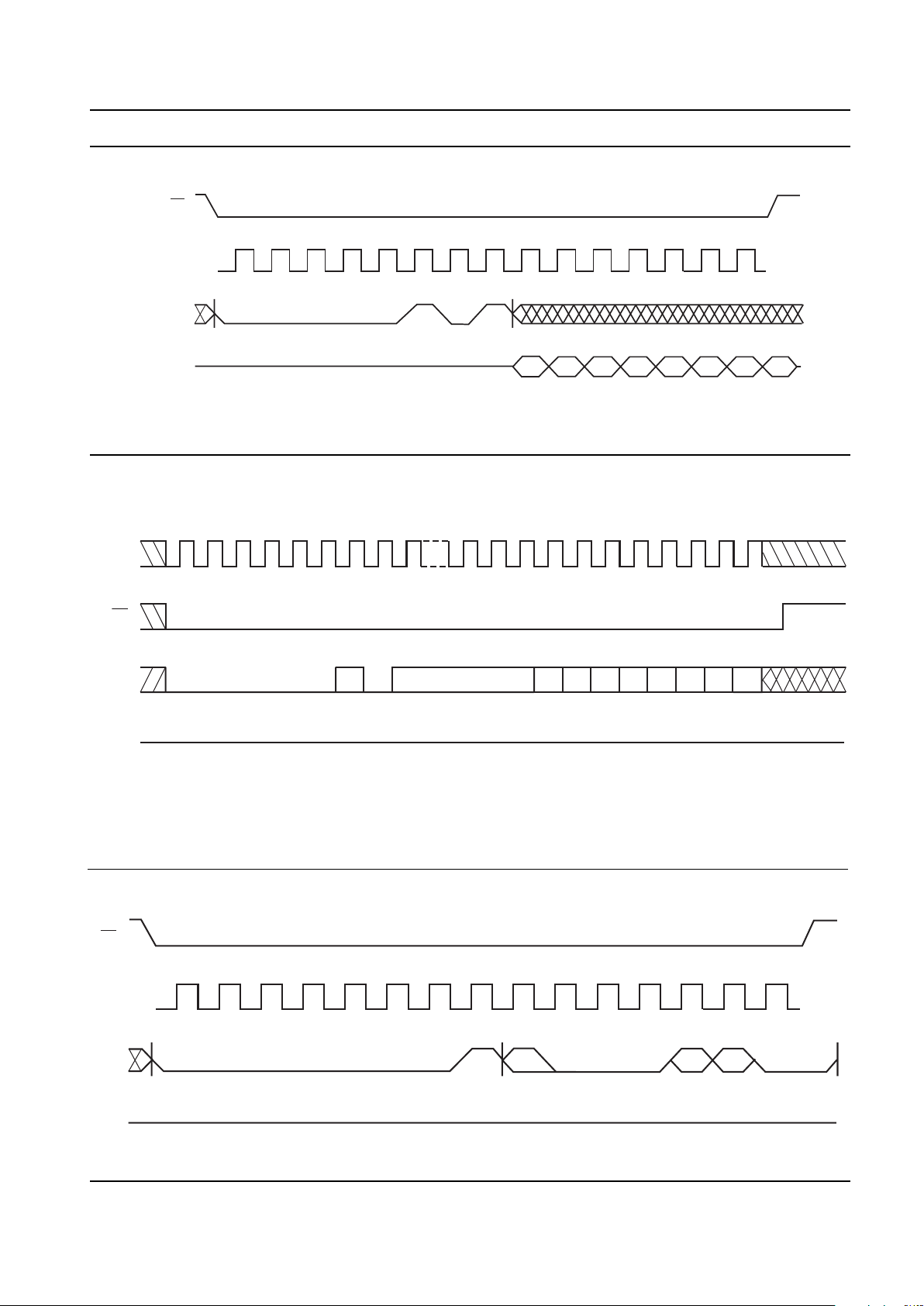
Figure 4. Read Instruction Timing
SK
SI
CS
SO
RESET
00000011
BYTE ADDRESS*
012345678910 2021222324252627282930
7 6 5 4 3 2 1 0
*Please check the instruction set table for address
Figure 3. WRDI Instruction Timing
SK
SI
CS
SO
0
0
000100
HIGH-Z
25C128 F05
9-103
CAT25CXXX
Stock No. 21085-01 4/98
Advanced
Figure 7. WRSR Timing
25C128 F08
012345678 10911121314
67453210
CS
SCK
SI
SO
INSTRUCTION
DATA IN
Figure 6. Write Instruction Timing
SK
SI
CS
SO
0 0 0 0 0 0 1 0 ADDRESS
D7 D6 D5 D4 D3 D2 D1 D0
012345678 2122232425262728293031
Figure 5. RDSR Timing
25C128 F09
012345678 10911121314
67453210
CS
SCK
SI
SO
HIGH IMPEDANCE
MSB
DATA OUT

9-104
CAT25CXXX
Stock No. 21085-01 4/98
Advanced
DEVICE OPERATION FOR THE
SUPERVISORY CIRCUIT
Reset Controller Description
The CAT25CXXX provides a precision RESET controller that ensures correct system operation during brownout and power-up/down conditions. It is configured
with open drain RESET outputs. During power-up, the
RESET outputs remain active until VCC reaches the
V
TH
threshold and will continue driving the outputs for
approximately 200ms (t
PURST
) after reaching V
TH.
After
the t
PURST
timeout interval, the device will cease to drive
reset outputs. At this point the reset outputs will be
pulled up or down by their respective pull up/pull down
devices. During power-down, the RESET outputs will
begin driving active when VCC falls below V
TH.
The
RESET outputs will be valid so long as VCC is >1.0V
(V
RVALID
).
The RESET pins are I/Os; therefore, the CAT25CXXX
can act as a signal conditioning circuit for an externally
applied reset. The inputs are level triggered; that is, the
RESET input in the 25CXXX will initiate a reset timeout
after detecting a high and the RESET input in the
25CXXX will initiate a reset timeout after detecting a low.
Watchdog Timer
The Watchdog Timer provides an independent protection for microcontrollers. During a system failure, the
CAT25CXXX will respond with a reset signal after a
time out period (the time out period is defined by the
watchdog timer bits WD0 an d WD1) for lack of activity.
25CXXX is designed with the Watchdog Timer feature
on the CS input. For the 25CXXX, if the microcontroller
does not toggle the CS pin within the time out period the
Watchdog Timer times out. This will generate a reset
condition on reset outputs. The Watchdog Timer is
cleared by any transition on CS.
As long as the reset signal is asserted, the Watchdog
Timer will not count and will stay cleared.
Reset Threshold Voltage
From the factory the 25CXXX is offered in six different
variations of reset threshold voltages. They are 4.50-
4.75V, 4.25-4.50V, 3.00-3.15V, 2.85-3.00V, 2.55-2.70V
and 1.7-1.8V. To provide added flexibility to design
engineers using this product, the 25CXXX is designed
with an additional feature of programming the reset
threshold voltage. This allows the user to change the
existing reset threshold voltage to one of the other five
reset threshold voltages. Once the reset threshold
voltage is selected it will not change even after cycling
the power, unless the user uses the programmer to
change the reset threshold voltage. However, the
programming function is available only through third
party programmer manufacturers. Please call Catalyst
for a list of programmer manufacturers who support this
function.
Figure 8. Page Write Instruction Timing
SK
SI
CS
SO
0 0 0 0 0 0 1 0 ADDRESS
Data
Byte 1
012345678 212223
24-31
32-39
Data
Byte 2
Data
Byte 3
Data
Byte N

9-105
CAT25CXXX
Stock No. 21085-01 4/98
Advanced
Symbol Parameter Min. Max. Units
t
GLITCH
Glitch Reject Pulse Width 100 ns
V
RT
Reset Threshold Hystersis 15 mV
V
OLRS
Reset Output Low Voltage (I
OLRS
=1mA) 0.4 V
V
OHRS
Reset Output High Voltage Vcc-0.75 V
Reset Threshold (Vcc=5V) 4.50 4.75
(25CXXX-45)
Reset Threshold (Vcc=5V) 4.25 4.50
(25CXXX-42)
Reset Threshold (Vcc=3.3V) 3.00 3.15
(25CXXX-30)
Reset Threshold (Vcc=3.3V) 2.85 3.00
(25CXXX-28)
Reset Threshold (Vcc=3V) 2.55 2.70
(25CXXX-25)
Reset Threshold (Vcc=1.8V) 1.70 1.80
(25CXXX-17)
t
PURST Power-Up Reset Timeout 130 270 ms
t
RPD V
TH
to RESET Output Delay 5 µs
V
RVALID
RESET Output Valid 1 V
RESET CIRCUIT CHARACTERISTICS
V
V
TH
Figure 9. RESET Output Timing
GLITCH
t
V
CC
PURST
t
PURST
t
RPD
t
RVALID
V
V
TH
RESET
RESET
RPD
t

9-106
CAT25CXXX
Stock No. 21085-01 4/98
Advanced
Notes:
(1) The device used in the above example is a 25C161SI-30TE13 (RESET, SOIC, Industrial Temperature, 3.0-3.15 Reset Threshold
Voltage, Tape & Reel)
ORDERING INFORMATION
DESIGN CONSIDERATIONS
The CAT25CXXX powers up in a write disable state and
in a low power standby mode. A WREN instruction must
be issued to perform any writes to the device after power
up. Also,on power up CS should be brought low to enter
a ready state and receive an instruction. After a successful byte/page write or status register write the
CAT25CXXX goes into a write disable mode. CS must
be set high after the proper number of clock cycles to
start an internal write cycle. Access to the array during
an internal write cycle is ignored and programming is
continued. On power up,SO is in a high impedance. If
an invalid op code is received, no data will be shifted into
the CAT25CXXX, and the serial output pin (SO) will
remain in a high impedance state until the falling edge
of CS is detected again.
The VCC sense provides write protection when VCC falls
below the reset threshold value (VTH). The VCC lock out
inhibits writes to the serial EEPROM whenever VCC falls
below (power down) VTH or until VCC reaches the reset
threshold (power up) VTH.
Package
P = PDIP
S = 8-pin SOIC
S16 = 16-pin SOIC
U14 = 14-pin TSSOP
Prefix Device # Suffix
25C16
S
I
TE13
Product
Number
25C32: 32K
25C16:16K
25C08: 8K
25C04: 4K
25C02: 2K
Tape & Reel
TE13: 2000/Reel
CAT
Temperature Range
Blank = Commercial (0˚C to +70˚C)
I = Industrial (-40˚C to +85˚C)
A = Automotive (-40˚ to +105˚C)*
* -40˚C to +125˚C is available upon request
Optional
Company ID
-30
Reset Threshold
V oltage
45: 4.5-4.75V
42: 4.25-4.5V
30: 3.0-3.15V
28: 2.85-3.0V
25: 2.55-2.7V
17: 1.7-1.8V
1
RESET
1. RESET
2. RESET
 Loading...