

CTLST CAT24C02CWI-1.8, CAT24C02CWI, CAT24C02CWA-1.8, CAT24C02CWA, CAT24C02CW-1.8 Datasheet
...
1
CAT24C02C
2K-Bit Serial E2PROM
* Catalyst Semiconductor is licensed by Philips Corporation to carry the I2C Bus Protocol.
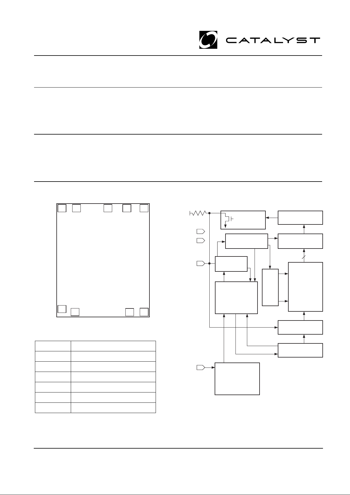
DIE PAD CONFIGURATION
BLOCK DIAGRAM
PIN FUNCTIONS
Pin Name Function
NC No Connect
SDA Serial Data/Address
SCL Serial Clock
V
CC
+1.8V to +6.0V Power Supply
V
SS
Ground
DC Don't Connect
FEATURES
■ 400 KHZ I
2
C Bus Compatible*
■ 1.8 to 6.0Volt Operation
■ Low Power CMOS Technology
■ Page Write Buffer
■ Self-Timed Write Cycle with Auto-Clear
■ 1,000,000 Program/Erase Cycles
■ 100 Year Data Retention
DESCRIPTION
The CAT24C02C is a 2K-bit Serial CMOS E2PROM
internally organized as 256 words of 8 bits each. Catalyst’s
advanced CMOS technology substantially reduces device power requirements. The the CAT24C02C features
a 16-byte page write buffer. The device operates via the
I2C bus serial interface and has a ISO 7816 compatible
pinout.
© 1999 by Catalyst Semiconductor, Inc.
Characteristics subject to change without notice
Doc. No. 25086 -00 8/99 S-1
D
OUT
ACK
SENSE AMPS
SHIFT REGISTERS
CONTROL
LOGIC
WORD ADDRESS
BUFFERS
STAR T/STOP
LOGIC
STATE COUNTERS
SLAVE
ADDRESS
COMPARATORS
E2PROM
V
CC
EXTERNAL LOAD
COLUMN
DECODERS
XDEC
DATA IN STORAGE
HIGH VOL TAGE/
TIMING CONTROL
V
SS
SCL
SDA
NC NC
DC
DCDC
V
SS
V
CC
SCL
SDA
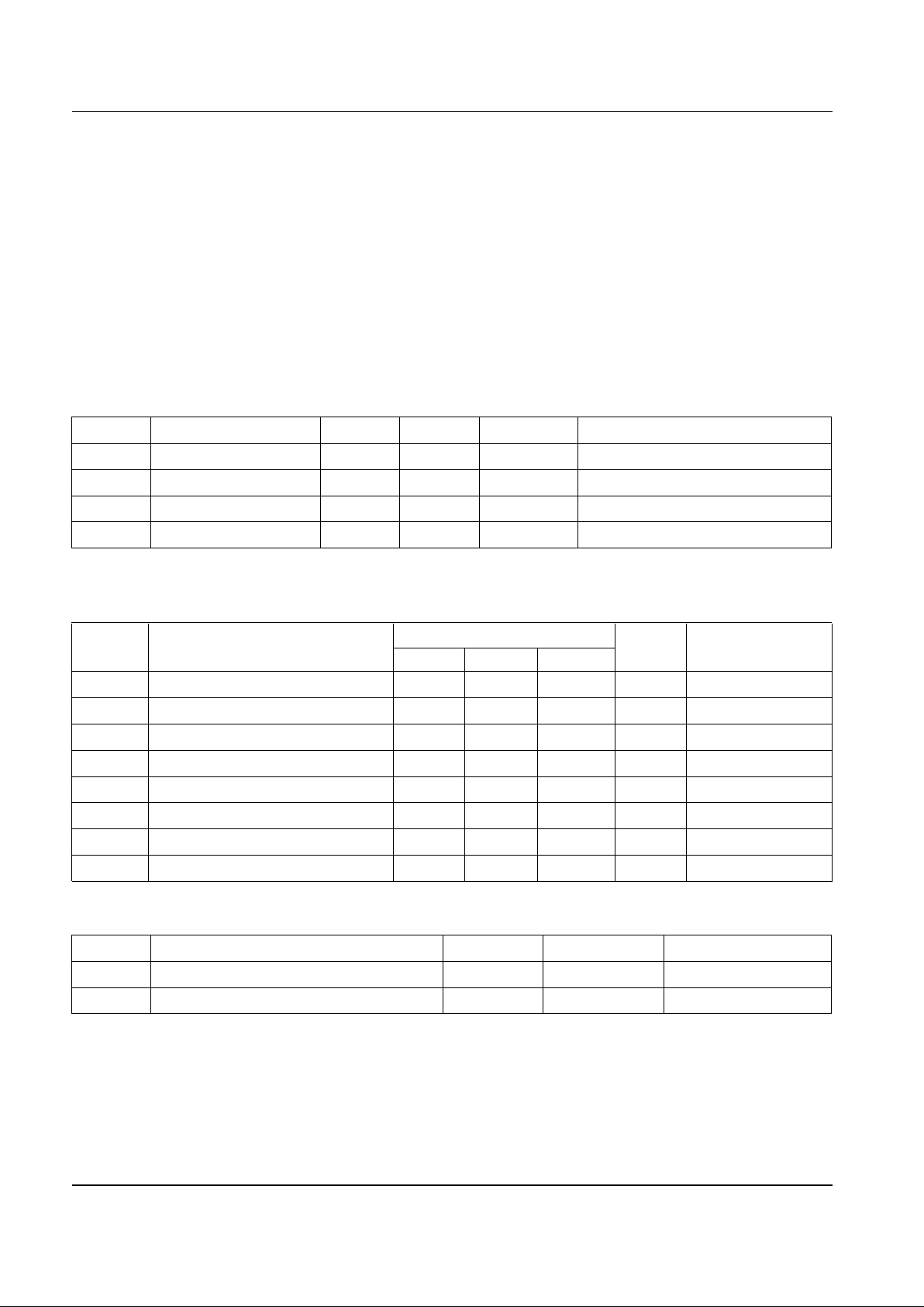
CAT24C02C
2
Doc. No. 25086-00 8/99 S-1
ABSOLUTE MAXIMUM RATINGS*
Temperature Under Bias ................. –55°C to +125°C
Storage Temperature....................... –65°C to +150°C
Voltage on Any Pin with
Respect to V
SS
(1)
................. –2.0V to +V
CC
+ 2.0V
VCC with Respect to V
SS
................................
–2.0V to +7.0V
Package Power Dissipation
Capability (Ta = 25°C)................................... 1.0W
Lead Soldering Temperature (10 secs) ............ 300°C
Output Short Circuit Current
(2)
........................ 100mA
*COMMENT
Stresses above those listed under “Absolute Maximum
Ratings” may cause permanent damage to the device.
These are stress ratings only, and functional operation of
the device at these or any other conditions outside of those
listed in the operational sections of this specification is not
implied. Exposure to any absolute maximum rating for
extended periods may affect device performance and
reliability.
RELIABILITY CHARACTERISTICS
Symbol Parameter Min. Max. Units Reference Test Method
N
END
(3)
Endurance 1,000,000 Cycles/Byte MIL-STD-883, Test Method 1033
T
DR
(3)
Data Retention 100 Years MIL-STD-883, Test Method 1008
V
ZAP
(3)
ESD Susceptibility 2000 Volts MIL-STD-883, Test Method 3015
I
LTH
(3)(4)
Latch-up 100 mA JEDEC Standard 17
D.C. OPERATING CHARACTERISTICS
VCC = +1.8V to +6.0V, unless otherwise specified.
Limits
Symbol Parameter Min. Typ. Max. Units Test Conditions
I
CC
Power Supply Current 3 mA f
SCL
= 100 KHz
I
SB
(5)
Standby Current (VCC = 5.0V) 0 µAVIN = GND or V
CC
I
LI
Input Leakage Current 10 µAVIN = GND to V
CC
I
LO
Output Leakage Current 10 µAV
OUT
= GND to V
CC
V
IL
Input Low Voltage –1 VCC x 0.3 V
V
IH
Input High Voltage VCC x 0.7 VCC + 0.5 V
V
OL1
Output Low Voltage (VCC = 3.0V) 0.4 V IOL = 3 mA
V
OL2
Output Low Voltage (VCC = 1.8V) 0.5 V IOL = 1.5 mA
Note:
(1) The minimum DC input voltage is –0.5V. During transitions, inputs may undershoot to –2.0V for periods of less than 20 ns. Maximum DC
voltage on output pins is VCC +0.5V, which may overshoot to VCC + 2.0V for periods of less than 20ns.
(2) Output shorted for no more than one second. No more than one output shorted at a time.
(3) This parameter is tested initially and after a design or process change that affects the parameter.
(4) Latch-up protection is provided for stresses up to 100 mA on address and data pins from –1V to VCC +1V.
(5) Standby Current (ISB) = 0µA (<900nA).
CAPACITANCE TA = 25°C, f = 1.0 MHz, VCC = 5V
Symbol Test Max. Units Conditions
C
I/O
(3)
Input/Output Capacitance (SDA) 8 pF V
I/O
= 0V
C
IN
(3)
Input Capacitance (SCL) 6 pF V
IN
= 0V
CAT24C02C
3
Doc. No. 25086-00 8/99 S-1
A.C. CHARACTERISTICS
VCC = +1.8V to +6.0V, unless otherwise specified.
Read & Write Cycle Limits
Symbol Parameter 1.8V, 2.5V 4.5V-5.5V
Min. Max. Min. Max. Units
F
SCL
Clock Frequency 100 400 kHz
T
I
(1)
Noise Suppression Time 200 200 ns
Constant at SCL, SDA Inputs
t
AA
SCL Low to SDA Data Out 3.5 1 µs
and ACK Out
t
BUF
(1)
Time the Bus Must be Free Before 4.7 1.2 µs
a New Transmission Can Start
t
HD:STA
Start Condition Hold Time 4 0.6 µs
t
LOW
Clock Low Period 4.7 1.2 µs
t
HIGH
Clock High Period 4 0.6 µs
t
SU:STA
Start Condition Setup Time 4.7 0.6 µs
(for a Repeated Start Condition)
t
HD:DAT
Data In Hold Time 0 0 ns
t
SU:DAT
Data In Setup Time 50 50 ns
t
R
(1)
SDA and SCL Rise Time 1 0.3 µs
t
F
(1)
SDA and SCL Fall Time 300 300 ns
t
SU:STO
Stop Condition Setup Time 4 0.6 µs
t
DH
Data Out Hold Time 100 100 ns
Note:
(1) This parameter is tested initially and after a design or process change that affects the parameter.
(2) t
PUR
and t
PUW
are the delays required from the time VCC is stable until the specified operation can be initiated.
The write cycle time is the time from a valid stop
condition of a write sequence to the end of the internal
program/erase cycle. During the write cycle, the bus
interface circuits are disabled, SDA is allowed to remain
high, and the device does not respond to its slave
address.
Write Cycle Limits
Symbol Parameter Min. Typ. Max Units
t
WR
Write Cycle Time 10 ms
Power-Up Timing
(1)(2)
Symbol Parameter Max. Units
t
PUR
Power-up to Read Operation 1 ms
t
PUW
Power-up to Write Operation 1 ms
 Loading...