

Page 1
Page 2

Page 3

Table of Contents
i
Chapter 1. Introduction …………………………………………... 1
1.1 General …………………………………………………….. 1
1.2 Functional Description ……………………………………. 1
1.3 Technical Specifications …………………………………... 3
1.4 T1 Signal Structure ……………………………………….. 4
1.5 Applications / Capabilities ………………………………… 6
Chapter 2. Installation ……………………………………………. 9
2.1 General …………………………………………………….. 9
2.2 Site Preparation …………………………………………… 9
2.3 Mechanical Assembly ……………………………………... 9
2.4 Electrical Installation ……………………………………… 10
2.5 Power Supply Modules …………………………………… 12
Chapter 3. Data Modules ………………………………………… 13
3.1 Data Modules Overview …………………………………... 13
3.2 Data Module LED Indicators …………………………….. 16
3.3 V.35 Data Module …………………………………………. 17
3.4 RS-530 Data Module ……………………………………… 18
3.5 RS-449 Data Module ……………………………………… 19
3.6 X.21 Data Module …………………………………………. 20
3.7 ET10 Ethernet Module ……………………………………. 21
Page 4

Table of Contents
ii
Chapter 4. Loop Back Testing …………………………………... 23
4.1 General ……………………………………………………... 23
4.2 User Activate Loop Back …………………………………. 23
4.3 T1 Link local digital loop back ……..…………….………. 23
4.4 Data Port local analog loop back ……………….………… 24
4.5 T1 Link remote loop back ………………………………… 24
4.6 BERT local loop back ……………...……………………… 25
4.7 BERT remote loop back for system test .………………… 25
Chapter 5. Troubleshooting ……………………………………… 27
5.1 General …………………………………………………….. 27
5.2 Connections .……………………………………………….. 27
5.3 Configuration ..…………………………………………….. 28
5.4 FT1 Card testing .………………………………………….. 29
Appendix A. DIP Switch Setting Tables ………………………. 33
Notes: …………………………………………………………………. 39
Technical Inquiry Card
Page 5

Chapter 1. Introduction
1 TRM-01 APR 2000
1.1 General
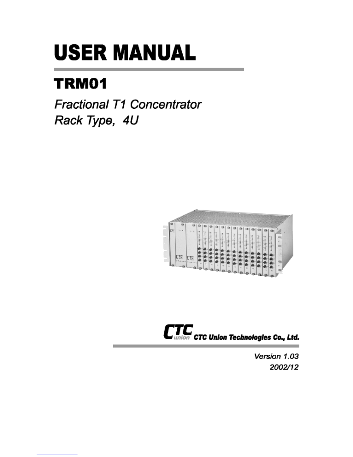
The TRM-01 is a 4U (7") high 19" Rack, containing multiple T1
CSU/DSUs for Fractional T1 network access. The TRM-01 provides an
economic solution in high density T1 installations such as central offices. There
are 13 slots available for installation of FT1 Cards (G.703 Fractional T1) into
the TRM-01 compact RACK. An optional SNMP Card may be installed into
the last slot, for local and remote management purposes, leaving 12 slots
available for FT1 Cards. Each FT1 Card may be linked to a remote TTU-01
or TTU-01A stand alone T1 CSU/DSU Access Unit to provide a variety of
LAN-to-LAN, Video Conference, Host to client, or Host to Host applications
over T1 Network Services.
1.2 Functional Description
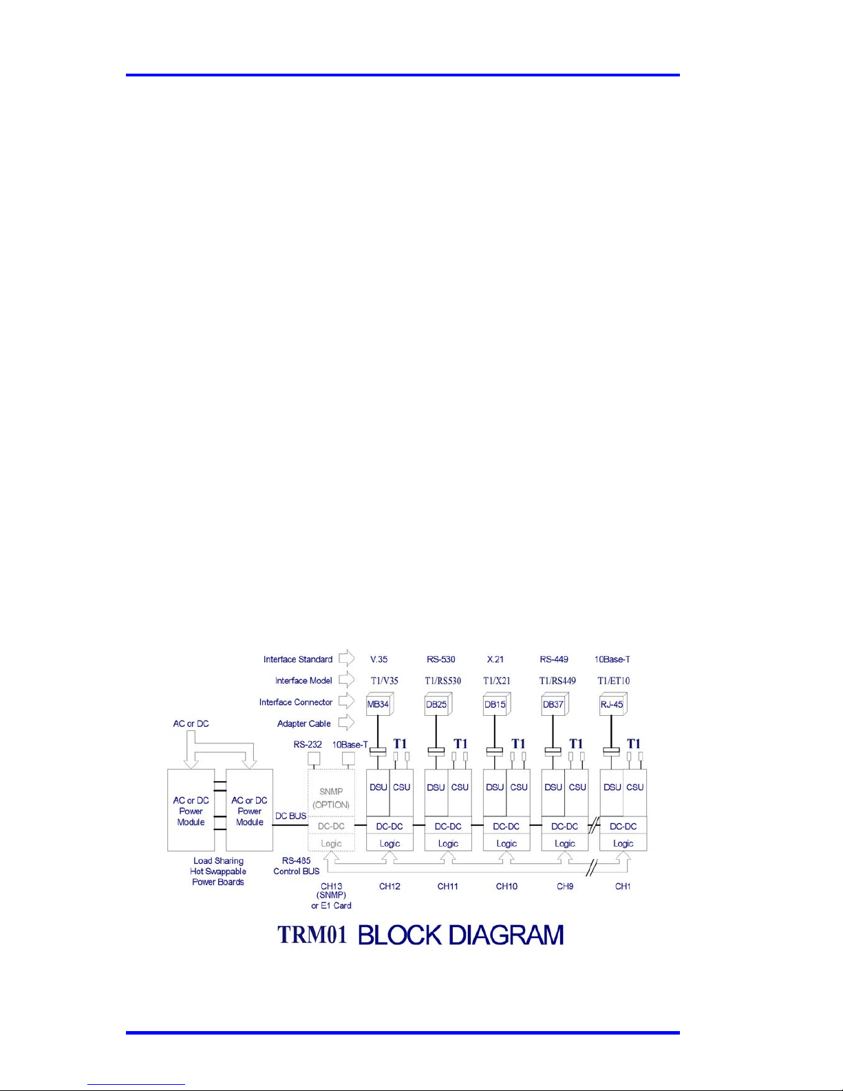
The TRM-01 may optionally incorporate two separate Power Module
supplies, which, depending on the model, may derive power from either an AC
power source (95~250VAC) or DC (-54 to -42VDC) power source. The power
supply modules provide for power redundancy and are hot swappable even
during the FT1 Cards' transmissions. The TRM-01 provides all interface
connections on the rear panel. BNC and Terminal Blocks are used for T1 Line
interface connections, while optional cable adapters are used to convert the
HDB26 DCE ports to V.35, RS-530, RS-449 or X.21. When an FT1/ET10
Card (Ethernet bridge interface) is installed in the TRM-01, the card can
provide either Ethernet bridging or repeating (non-filter mode) over the T1 link.
When cards are inserted in slots, LEDs on the front panel will show both the T1
Line and Data port statuses, Power Status, and any Alarm indications.
The FT1 Card data channels support user-selectable transmission rates,
which are integer multiples of 56Kbps or 64Kbps (fractional T1), up to a
maximum 2048Kbps (unframed T1), for a line attenuation of up to 43 dB on
twisted pair or coax cables. This provides an approximate operating range of up
to 2Km (over 22AWG wire).
The FT1 Card packs its data channel into user selected T1 link time slots.
The unused time slots may have IDLE code of 0xff or 0x7e inserted (in frame
mode) or they may insert the receive side time slot's data (In cascade mode).
The TRM-01 has three major types of FT1 Card data port interface
modules, which provide the desired interface: V.35, RS-530, or ET10 Ethernet.
X.21 and RS-449 interfaces are fully supported using the RS-530 (public) card
and appropriate X.21 and RS-449 adapter cables.
Page 6
Chapter 1. Introduction
2 TRM-01 APR 2000
The TRM-01 and FT1 Cards fully meet all T1 specifications including
ITU-T G.703, G.704, G.706, G.732, and G.823.
Each FT1 Card features V.54 diagnostic capabilities for performing local
loop back and remote loop back. The operator at either end of the T1 line may
test both the FT1 Card and the line in the digital loop back mode. The loop
back is controlled by either a manual push-button switch or by the DTE
interface for V.35 or RS-530.
When the local loop back switch is activated, an internal 511 bit pseudo
random test pattern is generated, according to ITU-T, for direct end-to-end
integrity testing. The Err indicator LED flashes for each bit error detected.
Multiple clock source selection provides maximum flexibility in
connecting both the T1 and user data interface. The T1 link may be clocked
from the recovered receive clock, from user data port, or from an on-card
oscillator.
When the TRM-01 is ordered with an optional SNMP Card, the card is
placed in slot number 13. Each FT1 Card will have DIP Sw7-6 turned ON to
enable remote setting. In this mode, the other DIP switch settings are ignored
while the SNMP Card controls all settings (with the exception of termination
impedance). Control is accomplished either via local control on the
asynchronous RS-232 port with an ASCII terminal or via Ethernet and any
standard SNMP network management software. If the SNMP Card option is
not installed, slot number 13 may hold an additional FT1 Card.
Figure 1-1 : TRM-01 Block Diagram
Page 7
Chapter 1. Introduction
3 TRM-01 APR 2000
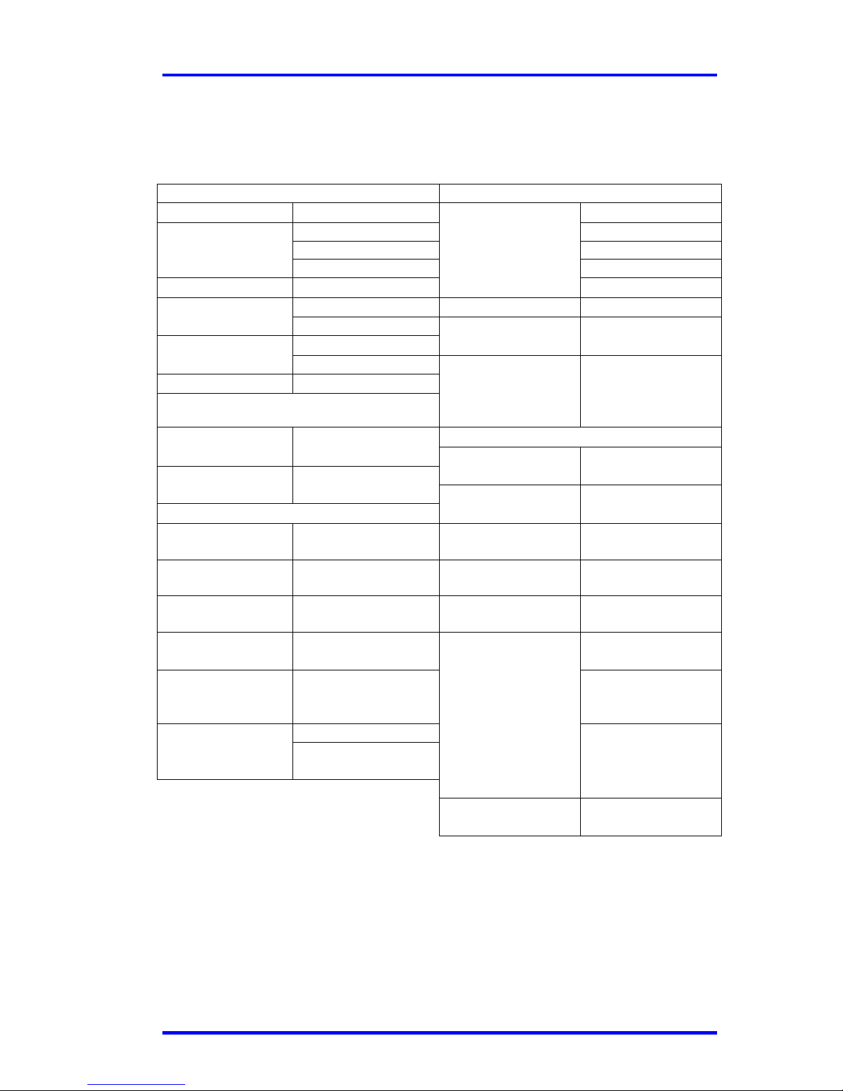
1.3 Technical Specifications
T1 Link User Data Channels
• Framing
Unframed/Framed V.35
D4(SF) RS-530
ESF RS-449
X.21
• Bit Rate
1.544Mbps
• Interface Type
Ethernet 10Base-T
AMI
• I/F Connectors
HDB26 female
• Line Code
B8ZS
100 Ω
• Line Code
NRZ (except
Ethernet)
• Line
Impedance
Balanced
• Receive Level
0 to –36dB
Transmit Level
• Data Rate
1536Kbps(unframe)
nx56 or nx64Kbps
where N equal
1 ~24
Clock Modes Pulse
amplitude
3.00V ±10% (100Ω)
Mode 0
(DCT1)
Rx and Tx clock
recovered from T1
Zero
amplitude
±0.1V
• Transmit Frequency Tracking
Mode 1
(DCE2)
Rx and Tx clock
internal oscillator
Internal
timing
±30ppm
Mode 2
(DTT1)
Sync to Rx clock
(transparent)
Loopback
timing
±50ppm
Mode 3
(DTE2)
Tx from ETC and
Rx from ERC
External
timing
±100ppm
Mode 4
(DTE3)
Tx and Rx both
from ETC
• Jitter
performance
According to ITU-T
G.824
CTS constantly ON
• Complies with
ITU-T G.703,G.704,
G.706,G.733,G824
and ANSI T1 403
DSR constantly ON
except during test
BNC for unbalanced
• I/F connectors
5 pin Molex ™ for
balanced
• Handshaking
control signals
DCD constantly ON
(except during
signal loss)
• Timeslot
Allocation
User Defined
Table 1-1 : TRM-01 Specifications
Page 8

Chapter 1. Introduction
4 TRM-01 APR 2000
1.4 T1 Signal Structure
The T1 line operates at a nominal rate of 1.544Mbps. The data transferred
over the T1 line is organized into frames, with each T1 frame containing 256
bits. The 256 bits are a total of the 24 time slots, each containing eight bits, that
carry the data payload.
T1 transmission utilizes two main types of framing: Superframe Format
(SF) and Extended Superframe Format (ESF). A T1 framing format that uses
the framing bit to provide maintenance and diagnostic functions. D4-frame - A
T1 line uses the D4 format, also known as the superframe (SF) format, to frame
data at the physical layer. The D4 format consists of 12 consecutive frames,
each separated by framing bits. Framing is necessary in order for equipment
receiving the T1 signal to be able to identify and extract the individual channels.
Superframe Format (SF)
SF - Also known as D4, T1 lines use this format to frame data at the
physical layer. The SF format consists of 12 consecutive frames, each separated
by framing bits.
Extended Superframe Format (ESF)
ESF is a framing format that consists of 24 consecutive frames separated
by framing bits. The ISDN specification advises that you use ESF with ISDN
D-channel signaling.
T1 line signal
The basic T1 line signal is coded using either the Alternate Mark
Inversion (AMI) or B8SZ rule.
Page 9

Chapter 1. Introduction
5 TRM-01 APR 2000
In the AMI format, “ones” are alternately transmitted as positive and
negative pulses, whereas “zeros” are transmitted as a zero voltage level. AMI is
not used in most 1.544Mbps transmissions because synchronization loss occurs
during long strings of data zeros.
B8ZS: Abbreviation for bipolar with eight-zero substitution . A T-carrier
line code in which bipolar violations are deliberately inserted if user data
contains a string of 8 or more consecutive zeros. Note 1: B8ZS is used to ensure
a sufficient number of transitions to maintain system synchronization when the
user data stream contains an insufficient number of "ones" to do so. Note 2:
B8ZS is used in the European hierarchy at the T1 rate.
T1 link line coding
The TRM-01 supports two T1 line codes:
AMI coding.
B8ZS coding.
T1 framing formats
The TRM-01 supports three frame formats:
Unframed format.
SF Superframe Format.
ESF Extended Superframe Format.
Page 10
Chapter 1. Introduction
6 TRM-01 APR 2000
1.5 Applications / Capabilities
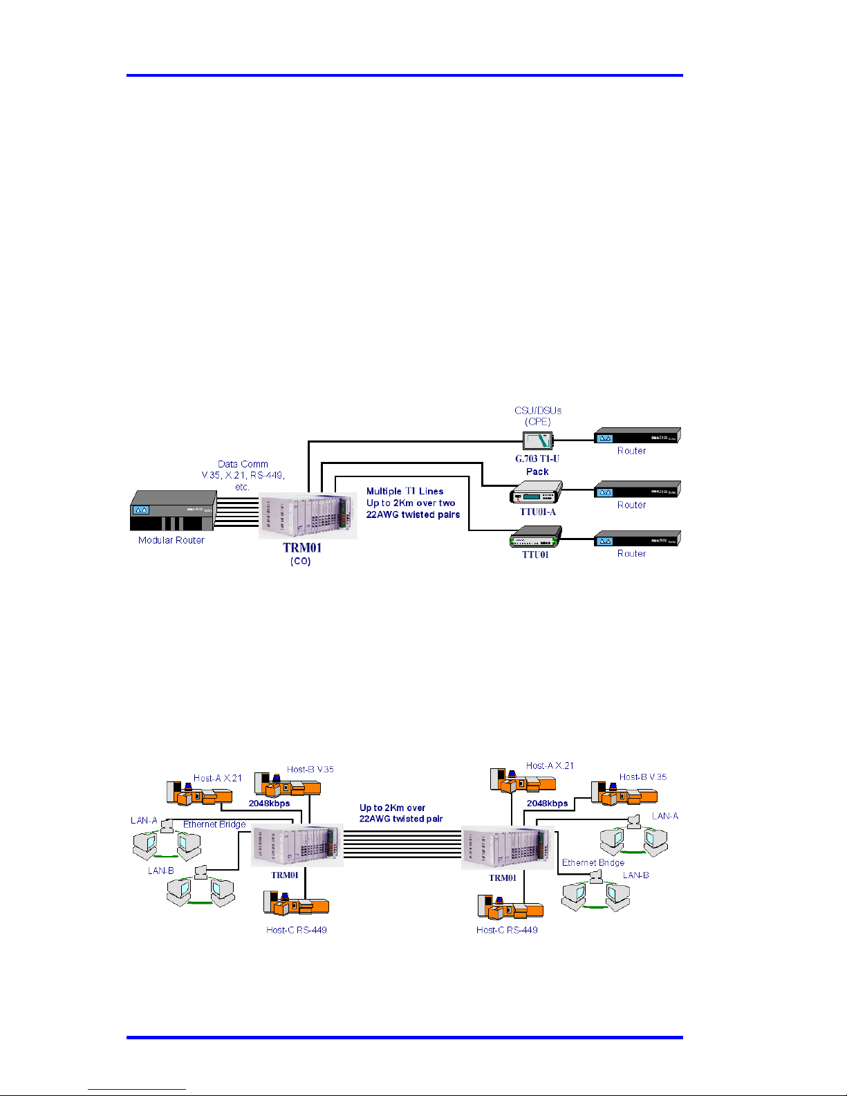
In the following example, the TRM-01 is installed at an ISP's central
office and provides "last mile" access to corporate customers over dedicated T1
transmission lines. The customer site utilizes a single data port CSU/DSU,
which could be one of our pack series or standalone units. While utilizing
fraction T1 connections, the ISP can provide a variety of bandwidth options to
its customers. By varying timeslot assignments, data rates from 64Kbps up to
1536Kbps may be utilized in frame mode.
The FT1 Cards in the TRM-01 could all be set to internal oscillator
timing or they could receive timing from the DTE on the data port. The remote
units would all be set to recovery.
Figure 1-2 : T1 nest for ISP
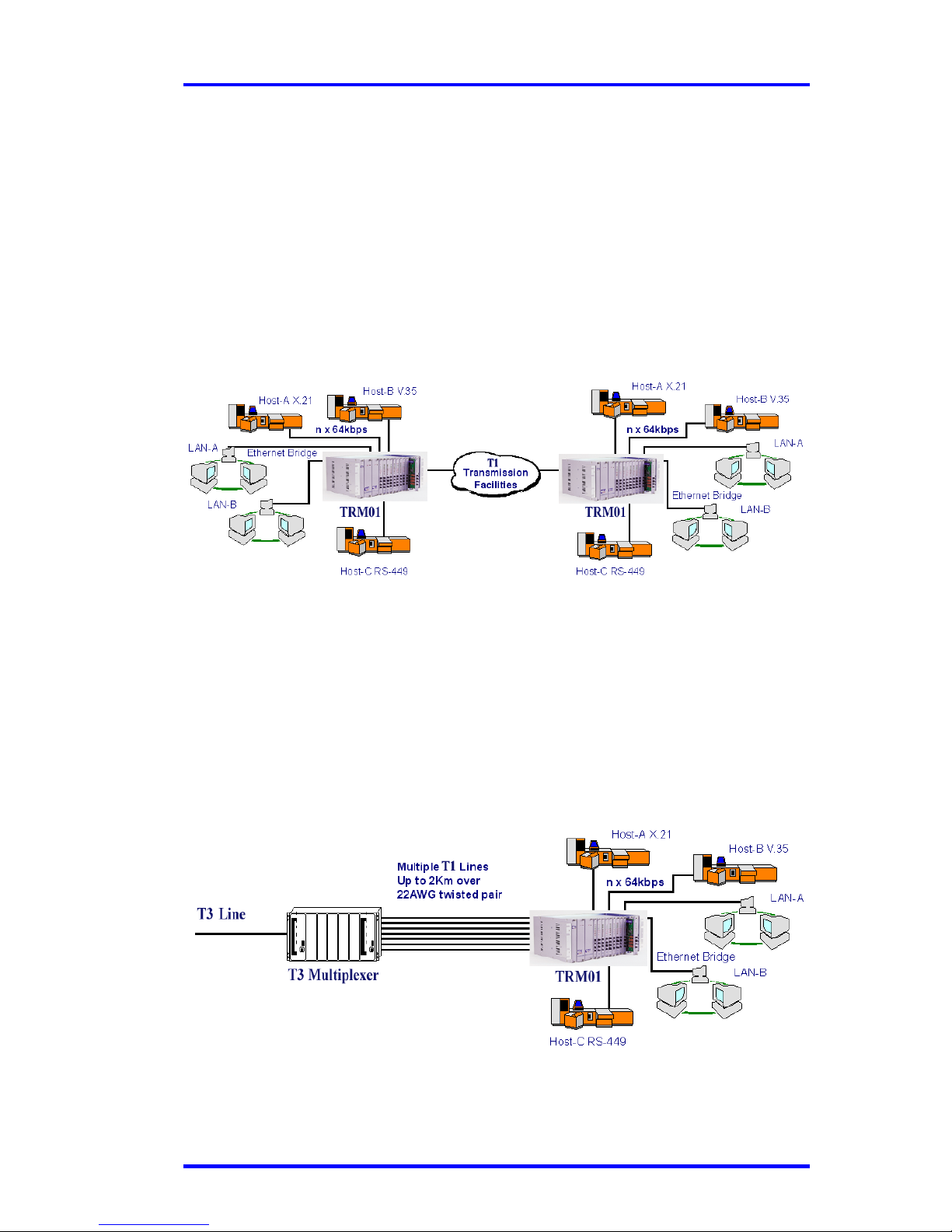
In the next application example, the TRM-01 is used in a point-to-point
T1 line environment. Each FT1 Card acts as a stand alone Digital Access Unit,
connecting individual T1 lines to data port interfaces or bridging Ethernet LANs.
For any T1 link, one CSU/DSU should provide internal timing while the linked
unit should be set to recovery.
Figure 1-3 : Point-to-point Application of TRM-01
Page 11
Chapter 1. Introduction
7 TRM-01 APR 2000
The next example utilizes the cascade capability of the FT1 Cards. In this
example, multiple FT1 Cards are set to “cascade”. Each card is assigned non-
overlapping timeslots of a single T1 line. In cascade mode, the FT1 Card
passes unused timeslot data transparently from Rx to Tx, creating a multiplexer
effect. By careful assignment of timeslots in the T1 frame, the TRM-01 could
be used as a 13 data channel multiplexer. It should also be noted however, that
removal or failure of any one card in this configuration would negatively effect
all other card data throughput.
Figure 1-4 : Multiplexer function (cascade mode) over T1 services
In the last application example, the TRM-01’s FT1 Cards provide
multiple data port connections via T1 lines connected through an T3 multiplexer
from an T3 line. Since the timing is normally passed from the network side, the
FT1 Cards should all be set to recovery.
Figure 1-5 : Multiple T1 Access via E3 multiplexer
Page 12

Chapter 1. Introduction
8 TRM-01 APR 2000
This page left blank intentionally.
Page 13
Chapter 2. Installation
9 TRM-01 APR 2000
2.1 General
This chapter explains in detail the requirements and procedures for the
installation of the TRM-01 Rack Mount Series T1 Digital Access Unit.
2.2 Site Preparation
Install the TRM-01 within reach of an easily accessible grounded AC
outlet. The outlet should be capable of furnishing 90 to 250 VAC. Allow at least
10cm (4 inch) clearance at the rear of the TRM-01 for signal lines and interface
cables.
2.3 Mechanical Assembly
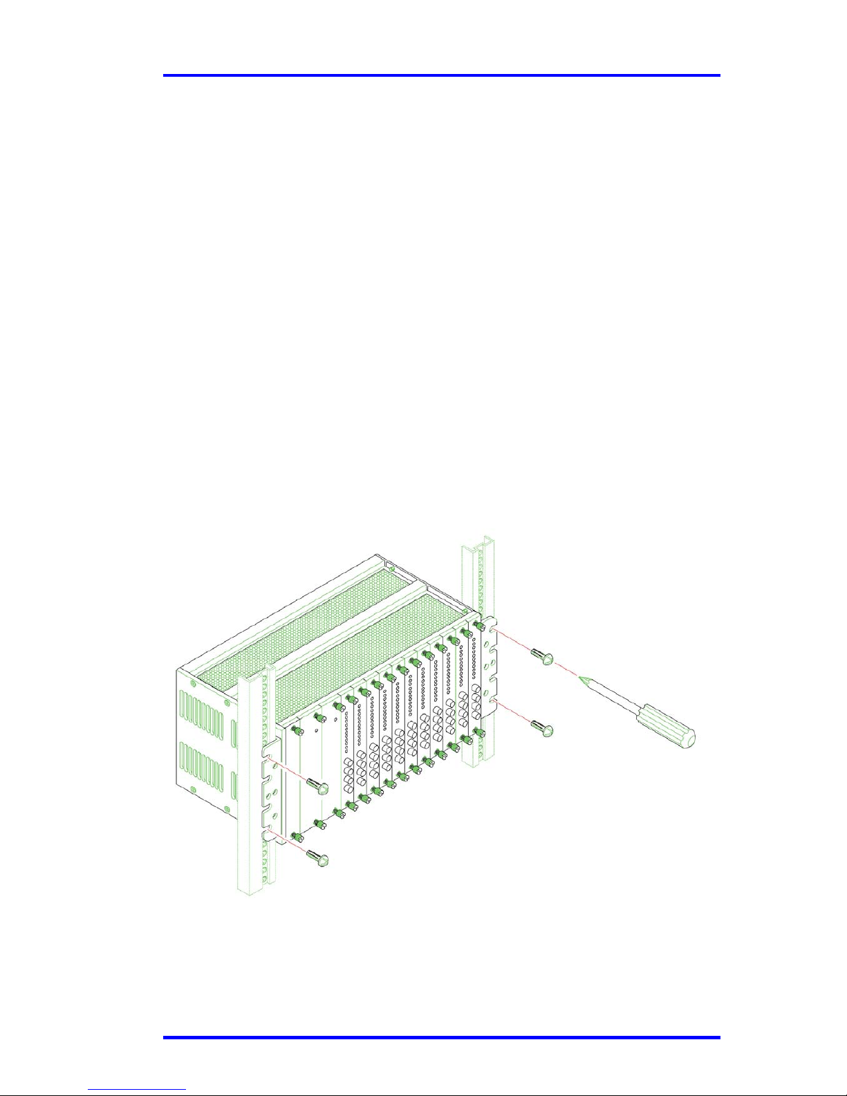
The TRM-01 is designed for rack mount installation and only requires 4U
space (7") in a standard EIA 19 inch rack. It is highly recommended that the
unit be placed in a rack. The TRM-01 is delivered completely assembled. No
provision is made for bolting the TRM-01 to a tabletop.
Figure 2-1 : Rackmount Installation of the TRM-01 Unit
Page 14
Chapter 2. Installation
10 TRM-01 APR 2000
2.4 Electrical Installation
2-4-1. Power connection
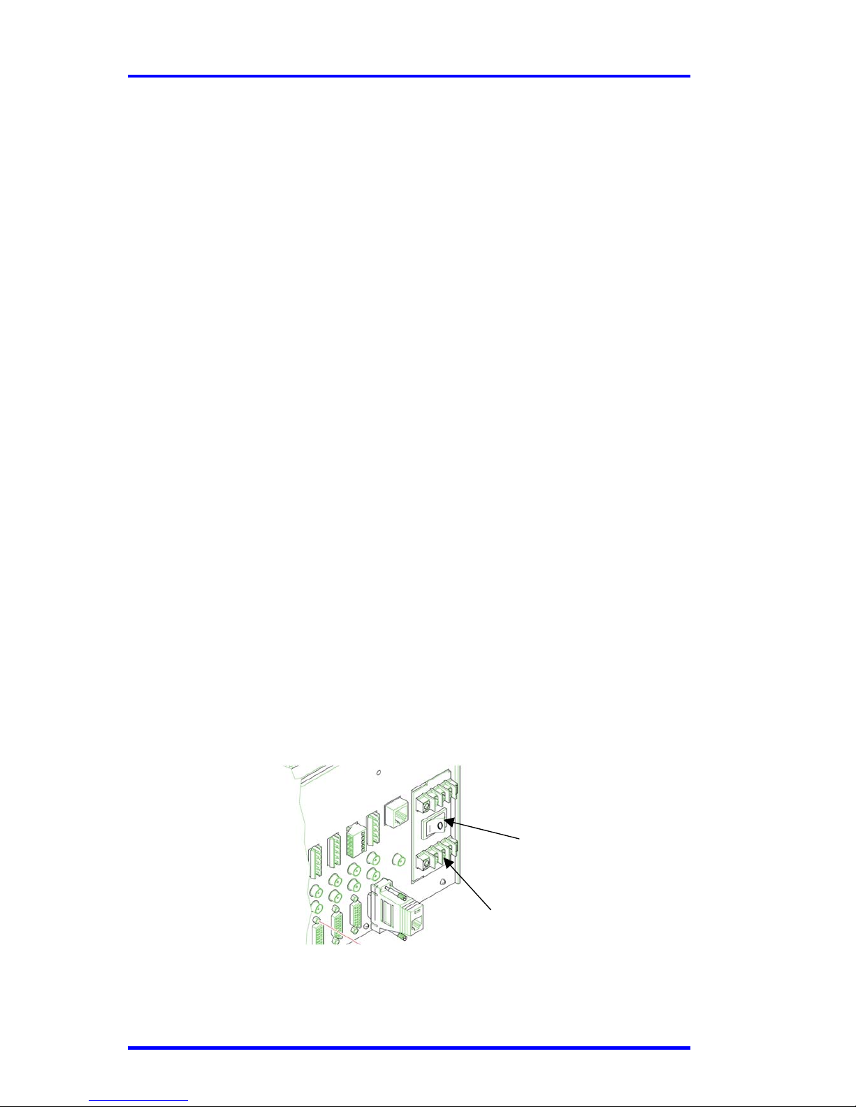
In the AC model, AC power is supplied to the TRM-01 through a standard
IEC 3-prong receptacle, located on the rear of the chassis. In the DC model,
DC –48V is connected to the lower terminal block, observing the proper
polarity. The TRM-01 should always be grounded through the protective earth
lead of the power cable in AC installations, or via the ground connection for DC
installations.
The line fuses for the TRM-01 are located on the Power Module units
themselves. Access to the fuses requires removal of the Power Module card.
The fuse, a 20mm type, is located in the fuse holder labeled "F1". Make sure
that only fuses of the same rating are used for replacement. Do not use repaired
fuses or short-circuit the fuse holder.
Figure 2-2 : Fuse Location on AC Power Module
Line
Fuse
Holder
Location
Power
Module
(one or two)
Mains
Switch
in back
TRM-01
Chassis
Page 15
Chapter 2. Installation
11 TRM-01 APR 2000
2-4-2. Rear panel connectors
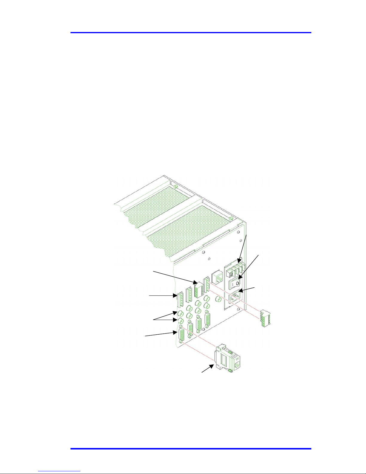
The FT1 Cards install into the front of the TRM-01 and receive DC
power from the back plane or “main board”. The back plane provides both DC
power to the T1 Cards and routes signals from the cards to the T1 (CSU) and
data port (DSU) connectors accessible at the rear of the TRM-01. Three
interface connector groups are provided for each slot. The T1 signals may use
either the Rx/Tx BNC pair for unbalanced transmissions or the 5pin Molex
connectors with terminal block adapters for balanced transmissions. The data
port connections are made with optional adapter cables, using a common panel
connector, HDB26F for all interfaces.
Figure 2-3 : TRM-01 Rear Panel Connections
HDB26F Data Port
T1 unbalanced BNCs
T1 balanced Molex
HDB26F to RJ-45
(
for FT1/ET10)
Molex to terminal
post adapter
Alarm Relay Contacts
Mains Switch
IEC AC Mains Input
Page 16
Chapter 2. Installation
12 TRM-01 APR 2000
2.5 Power Supply Modules
The Power Supply Modules in the TRM-01 are available in two
versions, AC or DC. The AC version supports input voltages of 90 to 250 volts
at frequencies of 50 to 60 Hertz. The DC version supports –42 to -54VDC input
voltage. Only one power supply module is required to power a completely full
rack. When two Power Supply Modules are installed, the supplies are hot
swappable, meaning any one supply may be removed and replaced without
impacting the operation of the TRM-01 Rack.
When an AC Power Module is used in the TRM-01, AC power enters
from the IEC mains input connector on the rear panel. AC power is supplied to
the AC Power Module card(s) when the mains toggle switch is closed. The AC
passes through the F1 fuse(s), located on the Power Module card(s). The AC
power is rectified and filtered before being passed to the regulator module. The
regulator module is factory adjusted to provide 48VDC to the back plane with
complete regulation and over-voltage, over-current, and over-temperature
protection.
When a DC Power Module is used in the TRM-01, DC –48V enters from
the terminal block on the rear panel (see Figure 2-4). DC power is supplied to
the DC Power Module card(s) when the mains toggle switch is closed. The DC
passes through the F1 fuse(s), located on the Power Module card(s). The DC
power passes through the rectifier and filtering circuits, which provide reverse
polarity protection before being passed to the DC-DC regulator module. The
regulator module is factory adjusted to provide 48VDC to the back plane with
complete regulation and over-voltage, over-current, and over-temperature
protection.
Figure 2-4 : DC Model Power Connection
3-pole terminal block
for –48VDC Input
plus Frame Ground
Mains Switch
Page 17
Chapter 3. Data Modules
13 TRM-01 APR 2000
3.1 Data Module Overview
The Data Modules for the TRM-01 are FT1 (fractional T1) Cards which
slide into the TRM-01 chassis, and interface with the pack panel “main board”.
The back panel provides an interface connection to the FT1 cards for power,
T1 connection, data port connection and control logic (for optional SNMP/local
management terminal). The cards are designed to be “hot” swappable, meaning
the TRM-01 chassis need not be powered off in order to replace a card or pull it
for configuration setting. Each FT1 Card has a protection fuse and its own on
card DC-DC regulator. Each FT1 Card in the TRM-01 receives the DC buss
48VDC and uses its own on-card DC to DC converter to derive the required
operating voltage of 5VDC. Removal and installation of FT1 cards with the
rack chassis under power will not effect the operation of other FT1 cards. The
one exception to this would be a case where the improper fuse (rated too high)
were placed on a defective FT1 card, causing the main AC or DC power
module's fuse(s) to open. It should also be noted, that the FT1 cards themselves
have no redundancy. Therefore, if a card is pulled from the chassis while the
communication link is active, the link will be broken.
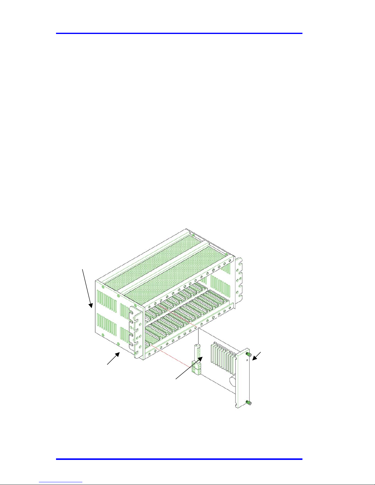
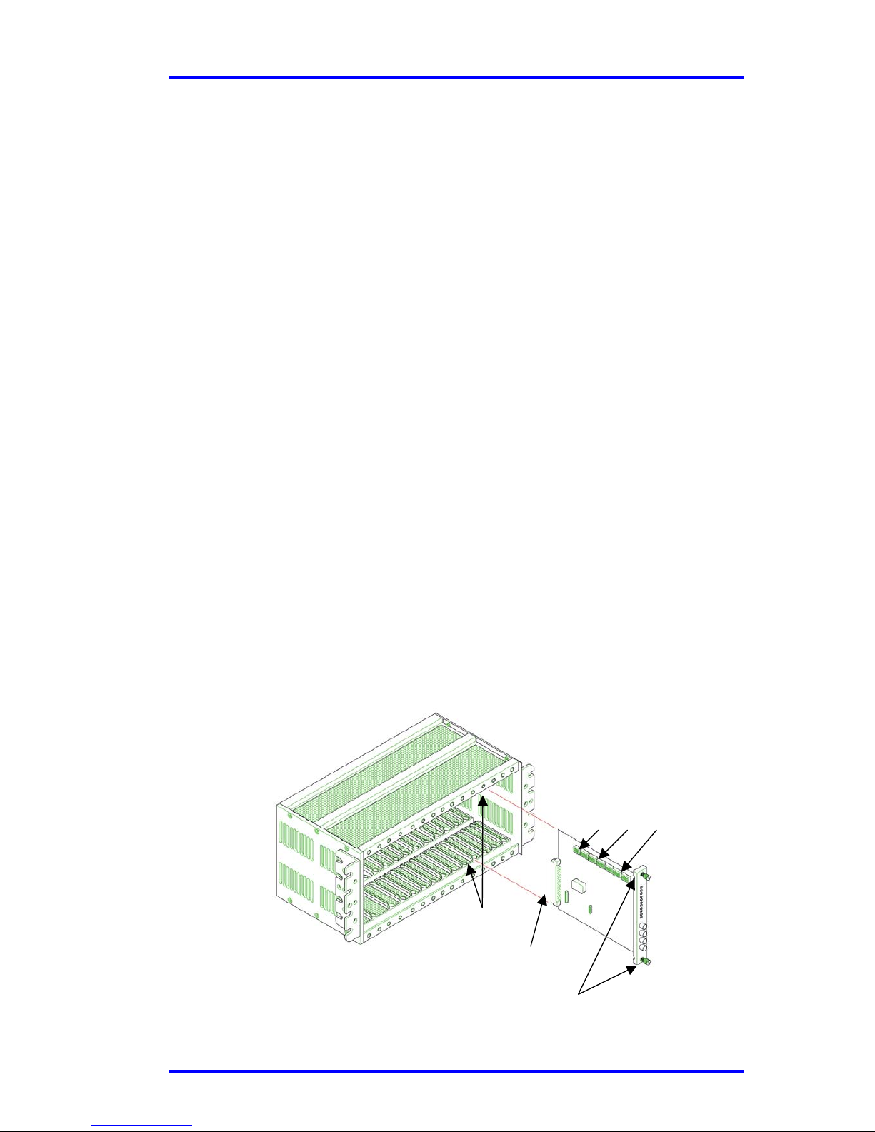
Removal of an FT1 Card is accomplished by loosing the two (2) captive
screws on the face plate of the card module, and then pulling the card straight
out of the chassis with the same screws. Apply equal pulling force to both top
and bottom captive screws to avoid the card binding in the rails of the chassis.
(refer to Figure 3-1) Replace the card by reversing the procedure, align in the
slot groove and gently seat the card. Retighten the captive screws.
Figure 3-1 : Removal/Replacement of FT1 Card in TRM-01 Chassis
Captive
Screws
TRM-01
Chassis
Card
Rails
Interface
Connector
FT1 Card
Configuration
DIP Switches
Page 18
Chapter 3. Data Modules
14 TRM-01 APR 2000
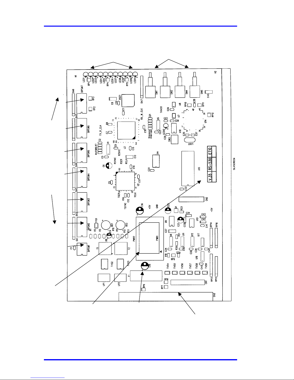
Figure 3-2 : FT1 Card Detail
Push button
switches
for Test
Loop Back
Power, Status
and
Alarm LEDs
9
Interface
Connector
DC-DC
Converter
Power
Protection
Fuse
Configuration DIP Switches
Hardware Version, I/F Type
Page 19

Chapter 3. Data Modules
15 TRM-01 APR 2000
The FT1 Card in the TRM-01 uses a common bare PC board. During
production, the card assembly is outfitted with the required interface circuitry
and firmware for a particular interface type. A check mark is placed in the box
as noted in the previous figure (shown with V.35 checked). The appropriate
interface adapter cable is then necessary for proper functioning. Care must
always be taken when swapping boards. Always check and match the correct
type. The three board types are RS-530 (public), V.35 and ET10 (Ethernet).
X.21 and RS-449 interfaces are fully supported by adapter cable paired to the
RS-530 (public) card.
There are seven (7) DIP (Dual Inline Package) Switches located along the
top of the FT1 Card numbered DIPSW1~7. The switches functions are to set
the T1 line connection impedance, frame mode, Time Slot allocation, clock
mode, line code, CRC, idle code, and data channel interface rate. Please refer to
Appendix A for the setting tables.
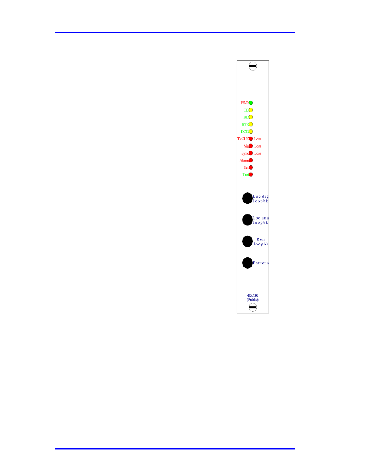
Located on the upper half of the front panel are the indicator LEDs. There
is a green power indicator which will light when the card is placed in an active
chassis. Failure of this LED to light indicates a possible power failure on the
FT1 Card itself. The TD, RD, RTS, and DCD yellow LEDs indicate status of
the data communication port. The red TxCLK, signal loss, sync loss and alarm
LEDs all indicate error conditions on the T1 line or link connection. When loop
back testing is being performed, the red test LED will light. If any bits are
received in error, the red err LED will flash.
Located on the lower half of the front panel are the manual test switches.
The top three switches set the type of loop back test to be performed. The
bottom switch enables the internal pattern generator. The Loc dig loopbk (local
digital loop back) switch tests the performance of the local FT1 Card, the
remote unit and the connections between by looping back the T1 received data
to the remote unit. The Loc ana loopbk (local analog loop back) switch tests the
performance of the local FT1 Card, the data terminal device and the
connections between by looping back the received terminal’s data back to the
terminal. The Rem loopbk (remote digital loop back) switch tests the
performance of the local and remote units, as well as the line, by issuing a
proprietary loop back command to the remote CSU/DSU. In order to perform
remote loop back, the FT1 Card must not be in unframed mode. When the
Pattern switch is depressed, the local FT1 Card sends out a 511-bit test pattern
(according to ITU-T V.54) on the T1 link, enabling testing of the entire link.
Refer to Chapter 4 for detailed diagrams of the loop back functions of the TRM-
01’s FT1 Card.
Page 20
Chapter 3. Data Modules
16 TRM-01 APR 2000
3.2 Data Module LED Indicators
PWR: This green LED should be lit when the chassis is
powered and the FT1 Card is seated in the rack slot.
TD: This yellow LED will flash when there is transmit data
activity from the connected DTE equipment to the FT1 Card.
RD: This yellow LED will flash when there is receive data
activity from the FT1 Card to the connected DTE equipment.
RTS: This yellow LED will be lit when the Request To Send
signal is active on the data port.
DCD: This yellow LED will be lit when the carrier signal is
active between the DSU and the connected DTE equipment.
TxCLK Loss: This red LED will light in the event of CSU
clock signal loss.
Sig Loss: This red LED will light in the event of CSU signal
loss.
Alarm: This red LED will light in the event of the following
alarm conditions: Remote Alarm Indication (RAI), Bi-Polar
Violation (BPV) error, All ones (AIS), CRC4 error, or Frame
Slip.
Err: This red LED will flash upon receiving an error while in
BERT mode (pattern depressed and looped back).
Test: This red LED will light if any of the test pushbuttons are
depressed or if the FT1 Card is in analog loop back due to
reception of a V.54 remote loop back code from the remote unit.
Figure 3-3 : FT1 Card face (RS530 public
card for RS-530, X.21, or RS-449)
Page 21

Chapter 3. Data Modules
17 TRM-01 APR 2000
3.3 V.35 Data Module
When the TRM-01 is ordered with an TRM01/V35 option, an FT1/V35
card is supplied and an optional V.35 adapter cable may be ordered or
assembled according to the following table. The adapter cable follows the pin
out standards shown below exactly.
Abbreviation HDB26
PIN#
MB34
PIN#
V.35
Circuit
FG 1 ↔ A Frame
SG 7 ↔ B Signal Ground
TD(A)
TD(B)
2
11
↔
↔
P S TD(A)
TD(B)
RD(A)
RD(B)
3
21
↔
↔
R T RD(A)
RD(B)
RTS(A) 4 ↔ C RTS
CTS(A) 5 ↔ D CTS
DSR(A) 6 ↔ E DSR
DTR(A) 20 ↔ H DTR
DCD(A) 8 ↔ F DCD
ETC(A)
ETC(B)
24
16
↔
↔
U W ETC(A)
ETC(B)
TC(A)
TC(B)
15
23
↔
↔
Y
AA
TC(A)
TC(B)
RC(A)
RC(B)
17
25
↔
↔
V X RC(A)
RC(B)
RLB 9 ↔ HH RL
LLB 18 ↔ JJ LL
TM 10 ↔ KK TM
Table 3-1 : HDB26 –MB34 adapter cable pin out for V.35
Page 22

Chapter 3. Data Modules
18 TRM-01 APR 2000
3.4 RS-530 Data Module
When the TRM-01 is ordered with an TRM01/530 option, an
FT1/530(public) card is supplied and an optional RS-530 adapter cable may be
ordered or assembled according to the following table. The adapter cable
follows the pin out standards shown below exactly.
Abbreviation HDB26
PIN#
DB25
PIN#
RS-530
Circuit
FG 1 ↔ 1 Frame
SG 7 ↔ 7 AB
TD(A)
TD(B)
2
11
↔
↔
2
14
BA(A)
BA(B)
RD(A)
RD(B)
3
21
↔
↔
3
16
BB(A)
BB(B)
RTS(A)
RTS(B)
4
13
↔
↔
4
19
CA(A)
CA(B)
CTS(A)
CTS(B)
5
14
↔
↔
5
13
CB(A)
CB(B)
DSR(A)
DSR(B)
6
22
↔
↔
6
22
CC(A)
CC(B)
DTR(A)
DTR(B)
20
12
↔
↔
20
23
CD(A)
CD(B)
DCD(A)
DCD(B)
8
26
↔
↔
8
10
CF(A)
CF(B)
ETC(A)
ETC(B)
24
16
↔
↔
24
11
DA(A)
DA(B)
TC(A)
TC(B)
15
23
↔
↔
15
12
DB(A)
DB(B)
RC(A)
RC(B)
17
25
↔
↔
17 9 DD(A)
DD(B)
RLB 9 ↔ 21 RL
LLB 18 ↔ 18 LL
TM 10 ↔ 25 TM
Table 3-2 : HDB26 –DB25 adapter cable pin out for RS-530
Page 23

Chapter 3. Data Modules
19 TRM-01 APR 2000
3.5 RS-449 Data Module
When the TRM-01 is ordered with an TRM01/449 option, an
FT1/530(public) card is supplied and an optional RS-449 adapter cable may be
ordered or assembled according to the following table. The adapter cable
follows the pin out standards shown below exactly.
Abbreviation HDB26
PIN#
DB37
PIN#
RS-449
Circuit
FG 1 ↔ 1 Frame
SG 7 ↔ 19,20,37 SG,RC,SC
TD(A)
TD(B)
2
11
↔
↔
4
22
SD(A)
SD(B)
RD(A)
RD(B)
3
21
↔
↔
6
24
RD(A)
RD(B)
RTS(A)
RTS(B)
4
13
↔
↔
7
25
RS(A)
RS(B)
CTS(A)
CTS(B)
5
14
↔
↔
9
27
CS(A)
CS(B)
DSR(A)
DSR(B)
6
22
↔
↔
11
29
DM(A)
DM(B)
DTR(A)
DTR(B)
20
12
↔
↔
12
30
TR(A)
TR(B)
DCD(A)
DCD(B)
8
26
↔
↔
13
31
RR(A)
RR(B)
ETC(A)
ETC(B)
24
16
↔
↔
17
35
TT(A)
TT(B)
TC(A)
TC(B)
15
23
↔
↔
5
23
ST(A)
ST(B)
RC(A)
RC(B)
17
25
↔
↔
8
26
RT(A)
RT(B)
RLB 9 ↔ 14 RL
LLB 18 ↔ 10 LL
TM 10 ↔ 18 TM
Table 3-3 : HDB26 –DB37 adapter cable pin out for RS-449
Page 24

Chapter 3. Data Modules
20 TRM-01 APR 2000
3.6 X.21 Data Module
When the TRM-01 is ordered with an TRM01/X21 option, an
FT1/530(public) card is supplied and an optional X.21 adapter cable may be
ordered or assembled according to the following table. The adapter cable
follows the pin out standards shown below exactly.
Abbreviation HDB26
PIN#
DB15
PIN#
X.21
Circuit
FG 1 ↔ 1 Shield
SG 7 ↔ 8 Ground
TD(A)
TD(B)
2
11
↔
↔
2 9 Transmit(A)
Transmit(B)
RD(A)
RD(B)
3
21
↔
↔
4
11
Receive(A)
Receive(B)
RTS(A)
RTS(B)
4
13
↔
3
10
Control(A)
Control(B)
DCD(A)
DCD(B)
8
26
↔
5
12
Indication(A)
Indication(B)
ETC(A)
ETC(B)
24
16
↔
↔
7
14
Ext. Timing(A)
Ext. Timing(B)
RC(A)
RC(B)
17
25
↔
↔
6
13
Signal Timing(A)
Signal Timing(B)
Table 3-4 : HDB26 –DB15 adapter cable pin out for X.21
Page 25
Chapter 3. Data Modules
21 TRM-01 APR 2000
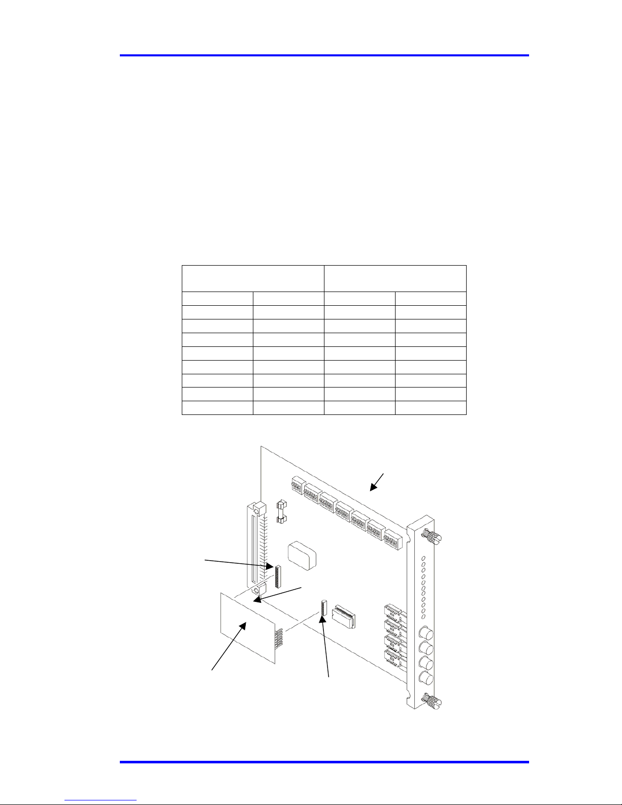
3.7 ET10 10Base-T Ethernet Bridge Module
When the TRM-01 is ordered with an TRM01/ET10 option, an
FT1/ET10 card and HDB26 to RJ-45 adapter are supplied and assembled
according to the following table. The FT1/ET10 Card includes an additional
“daughter” board to handle the Ethernet interface and Bridging functions. This
board has two (2) DIP switches which may only be accessed by removing the
daughter board. (Refer to Figure 3-4.) Pull the board straight out and avoid
bending the pins. After setting, press the daughter board back onto the FT1
Card, closely observing the 20 and 26 pin connectors.
Connection to HUB (1:1)
(depends on S1 setting)
Connection to PC (cross)
(depends on S1 setting)
HDB26 RJ-45 HDB26 RJ-45
11 1 T+ 11 1 R+
12 2 T- 12 2 R13 3 R+ 13 3 T+
14 4 14 4
15 5 15 5
16 6 R- 16 6 T17 7 17 7
18 8 18 8
Table 3-5 : HDB26 –RJ-45 adapter pin out for 10Base-T
Figure 3-4 : ET10 Daughter Board Removal/Replacement
20 pin
connector
ET10
Daughter Board
26 pin
connector
FT1/ET10
Ethernet Bridge Card
daughter board
DIP Switches S1&S2
Page 26
Chapter 3. Data Modules
22 TRM-01 APR 2000
ET10 : Attach to HUB (1:1) or PC (Crossover)
S1 === =x=
1 ON* OFF
2 ON* OFF
3 ON* OFF
4 ON* OFF
5 OFF* ON
6 OFF* ON
7 OFF* ON
8 OFF* ON
* factory setting
Table 3-6 : ET10 Daughter Board DIP Switch S1 Settings
S2 Set Comment Comment
1 ON* Factory Default Do not change
2 ON* Factory Default Do not change
3 ON* Factory Default Do not change
4 OFF* Factory Default Do not change
5 ON* Factory Default Do not change
6 X
OFF* = Full Duplex
ON = Half Duplex
7 X OFF* = Compression enabled ON = Compression disabled
8 X OFF* = Filter Disabled
(Repeater mode)
ON = Filter Enabled
(Bridge mode)
* factory setting
Table 3-7 : ET10 Daughter Board DIP Switch S2 Settings
SPECIFICATIONS
• BRIDGE
LAN Table: 10,000 MAC address with 5 minute automatic aging
Filtering and Forwarding: 15,000 frames/sec
Buffer: 256 frames
Delay: 1 frame
• LAN
Standard: Conforms to IEEE 802.3 / 10Base-T Ethernet
Data Rate: 10Mbps (20Mbps/ 10Base-T in Full duplex topology)
Filter:
When this feature is disabled (S2-8 OFF), all frames are passed transparently. In
this configuration, the ET10 acts as a repeater. When the filter is enabled, frame
destinations are tested against the internal MAC address table. Filtering enabled is the
normal selection for Bridging.
Compression:
Enhanced Tinygram Compression increases data throughput over the WAN.
Valid Ethernet frames have a minimum length of 64 bytes. Frames shorter than 64 bytes
are padded. With compression enabled (S2-7 OFF), these padding bytes are stripped off
before being transmitted over the WAN, and re-padded when received on the other side.
Page 27
Chapter 4. Loop Back Testing
23 TRM-01 APR 2000
4.1 General
In this chapter we shall explain the detailed functioning of the loop back
switches.
4.2 User Activated Loop back
The FT1 Card supports the following types of test loop backs.
Data Port local analog loop back.
T1 link local digital loop back.
T1 link remote loop back. (only works in CAS or CCS frame mode)
The user activated loop back functions may be accessed from the front
panel FT1 Card push-button switches, via the LOOPBACK PARAMETER
menu under ASCII terminal mode, or via SNMP. The latter two methods both
require the optional SNMP Card installed and will not be discussed any further
here. The available test functions via pushbutton switches are described on this
and the following pages.
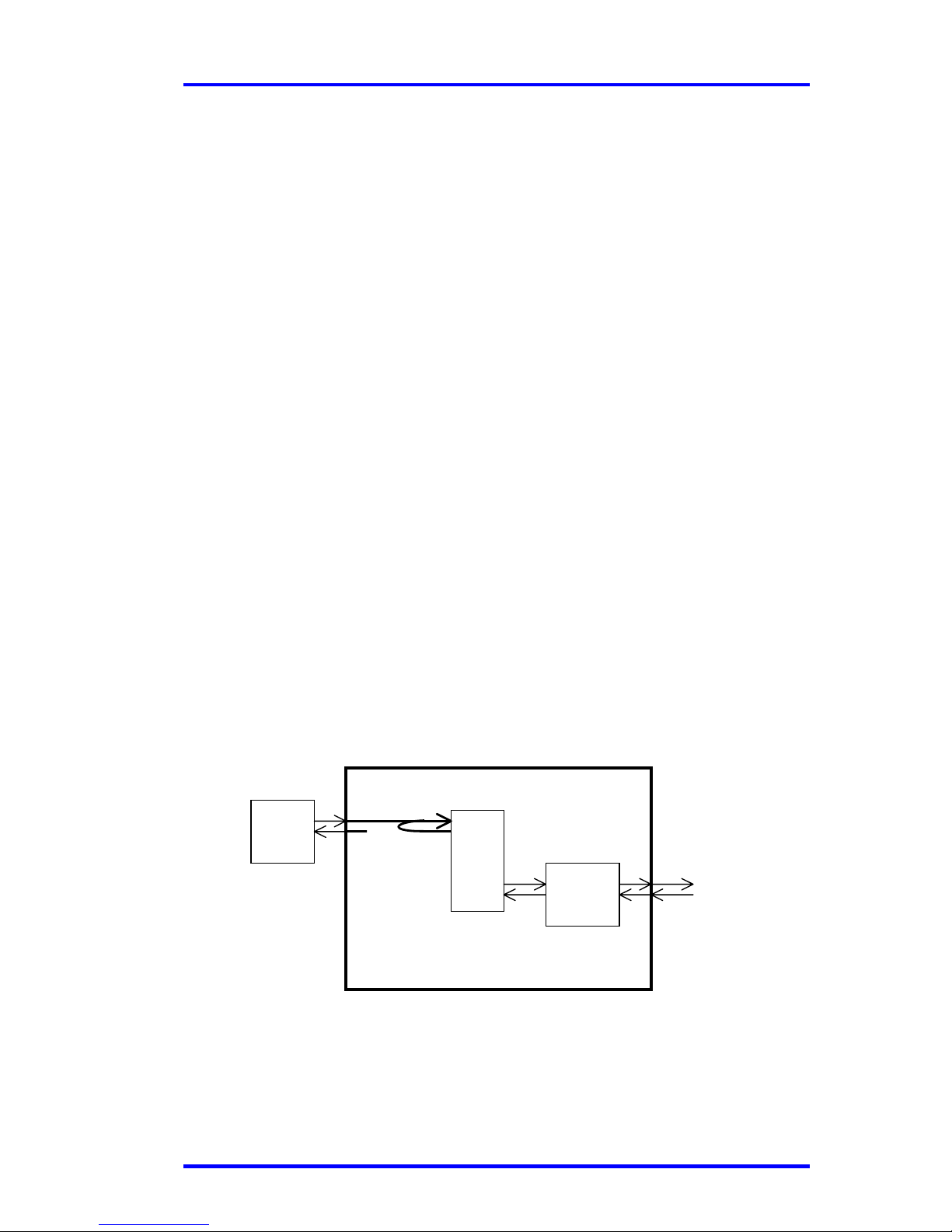
4.3 T1 link local digital loop back
The FT1 Card local digital loop back is established as close to the DTE
interface as possible to check the satisfactory working of the FT1 Card and the
T1 link connection. Using this setting, the remote CSU/DSU must supply the
test signal and verify it upon its return.
(Loc dig loopbk depressed)
Figure 4-1. T1 link local digital loop back
User
DTE
Data
Port
T1
CSU
LOCAL FT1 Card
Page 28
Chapter 4. Loop Back Testing
24 TRM-01 APR 2000
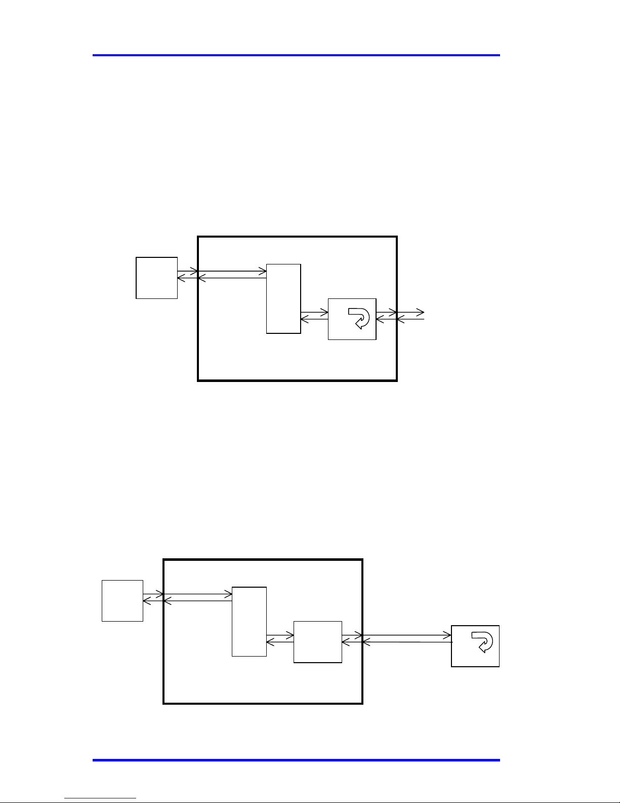
4.4 Data port local analog loop back
The FT1 Card local analog loop back is established in analog mode as
close as possible to the T1 line, to check the satisfactory working of the FT1
Card and the connection between the DTE and FT1 Card. This returns the
transmit signal of the Data port to the receive path of the Data port. The Data
Port must receive its own transmission, therefore we recommend never doing
this test when the data port is ET10 Ethernet bridge or collisions may result.
(Loc ana loopbk depressed)
Figure 4-2. Data port local analog loop back
4.5 T1 link remote loop back
The local FT1 Card signals the remote unit into digital loop back to
check satisfactory operation of the local FT1 Card, remote CSU/DSU and the
link between. If the User DTE is replaced with a BERT tester, the data cable,
FT1 Card, remote CSU/DSU and T1 link may all be tested.
(Rem loopbk depressed)
Figure 4-3. T1 link remote loop back
User
DTE
Data
Port
T1 to Remote
CSU
LOCAL FT1 Card
User
DTE
Data
Port
CSU
LOCAL FT1 Card
T1
link
Remote
CSU/DSU
loop back
code sent
Page 29
Chapter 4. Loop Back Testing
25 TRM-01 APR 2000
4.6 BERT local loop back
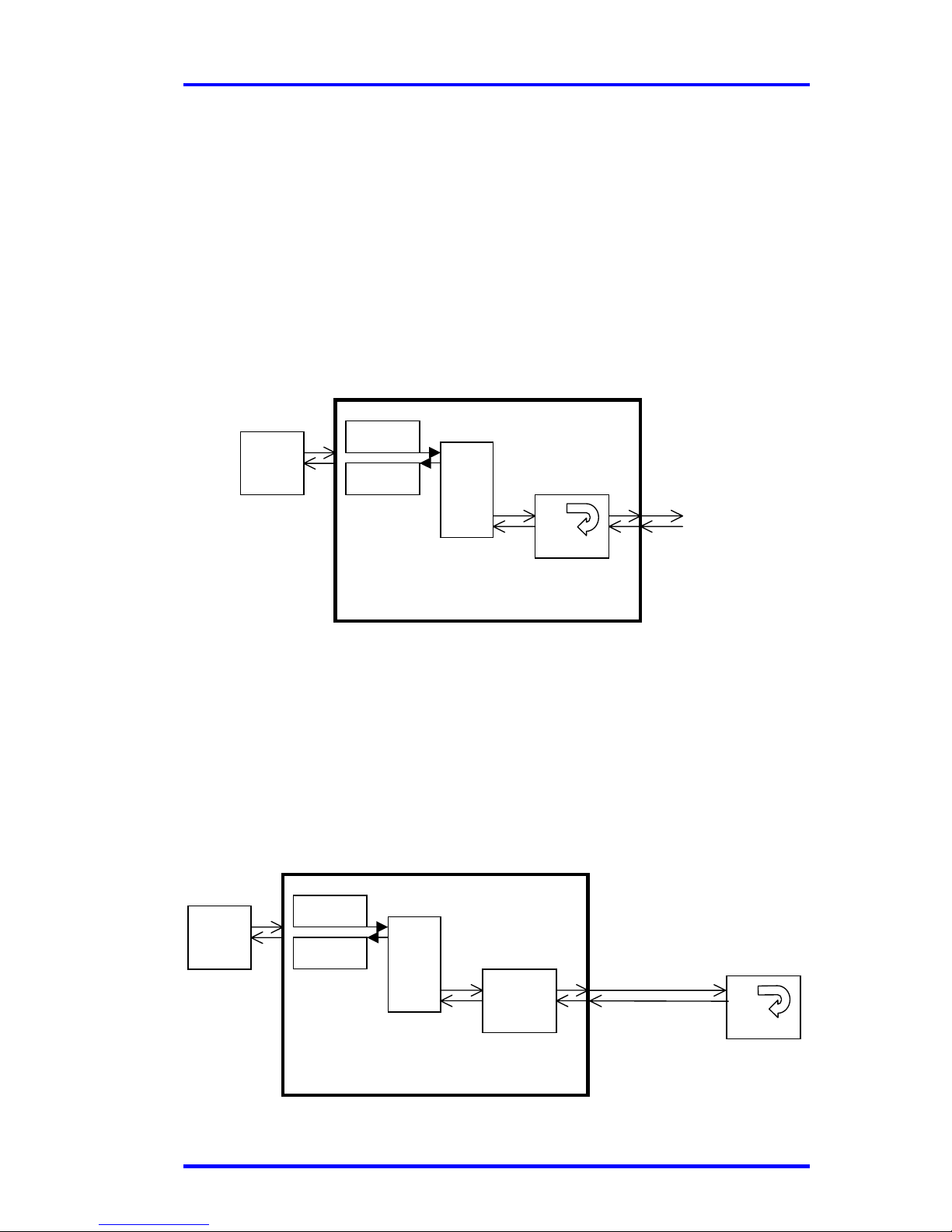
For a local test, depress the Loc ana loopbk pushbutton or physically
hardwire the T1 link TX to the T1 link RX with coaxial (BNC) cable. Depress
the Pattern push-button switch. During BERT testing, the local DTE is
disconnected and the DSR line is off. An internal 511-bit pattern will be
generated according to ITU-T and connected to the transmit input of the local
data channel interface. The receive output is connected to the pattern tester. The
tester compares the received and transmitted patterns and detects errors, as
shown in Figure 4-4. (Err LED should be off during successful loop back.)
(Pattern and Loc ana loopbk depressed)
Figure 4-4. BERT for local test
4.7 BERT remote loop back for system test
For a system test, the remote site CSU/DSU must support CTC's
proprietary remote loop back (Such as TTU-01 or another FT1 Card) and both
must be in matching frame mode. The local unit will depress both the Pattern
and Rem loopbk pushbutton switches. The entire T1 link may then be tested, as
shown in Figure 4-5.
(Rem loopbk and Pattern depressed)
Figure 4-5. BERT used for system test
User
DTE
Data
Port
T1
CSU
LOCAL FT1 Card
Generator
Tester
User
DTE
Data
Port
CSU
LOCAL FT1 Card
Generator
Tester
T1
link
Remote
CSU/DSU
loop back
code sent
Page 30

Chapter 4. Loop Back Testing
26 TRM-01 APR 2000
This page left blank intentionally
Page 31

Chapter 5. Troubleshooting
27 TRM-01 APR 2000
5.1 General
As in troubleshooting any type of computer, network, or communication
problem, it is very important to follow a very logical procedure. During any
troubleshooting session, the importance of taking notes cannot be overstated. It
is very easy to forget connections or settings when troubleshooting a large
network. Notes will help in logically checking all items and will also serve as a
valuable aid in writing a system log or other report to your supervisor or your
customer following successful completion of work. Notes also serve as
important tools for future troubleshooting or for training of new personnel or
just simply as a memory refresher.
When dealing with troubleshooting of first time installation problems, the
best place to start is with double-checking of configuration settings and
connections. It is very easy to misinterpret a DIP switch setting and cause the
failure of a link. Initial configuration problems will also cause either immediate
failure or inconsistent operations. Although the FT1 Cards all comply with ITU
G.703 recommendations, it is very important to understand the differences in
terminology between different equipment manufactures. A thorough
understanding of the settings and configuration of related equipment is
mandatory when integrating many vendors' equipment.
Having the proper tools is also important in any troubleshooting endeavor.
When troubleshooting T1 connections a transmission analyzer is an invaluable
tool in isolating configuration, line or hardware problems. CTC Union's BTM-
10 T1 Transmission Analyzer is an excellent choice. The unit is very portable,
battery operated, with built-in keyboard and LCD display. The tester is designed
to do BERT (Bit Error Rate) testing via T1 connection or via Data Port
connection at speeds up to 1.544Mbps.
5.2 Connections
When checking for connection related problems, start by looking for
physical defects in the connectors themselves. Check for broken or bent pins,
corrosion and mis-wiring. Check cables for pinching that could indicate a
broken or shorted wire. For twisted pair wiring, confirm that a wire pair actually
goes to the proper transmit or receive signal pairs. Build yourself an RJ-45
break-out-box from a pigtail converter. Loop back the pairs in the BOB and
confirm continuity with a multi-meter.
Page 32

Chapter 5. Troubleshooting
28 TRM-01 APR 2000
5.3 Configuration
When physical connections have been confirmed, start looking for
configuration problems. Confirm that the proper line code is being used. The
FT1 Cards all support AMI and B8ZS line codes. In almost all instances, the
line code will be B8ZS. Confirm settings.
Framing errors can result if setting errors are made. Confirm the mode,
whether which framed-format. If both sides of the T1 link are using different
framing, there will be alarm indications.
Data errors may result if the timeslot assignments in fractional mode do
not match. Check the settings carefully. For reduced monthly charges, a
customer may only request a fraction of the T1 bandwidth. In this instance, an
ISP may provide a fraction of the full 1.544Mbps bandwidth to a customer by
utilizing Fractional T1. If only 512Kbps is requested, only eight (8) timeslots
are required to carry the data payload. Carefully check the settings at the central
site and confirm that the same eight timeslots are active on each end of the link.
Configuration check list:
T1 Line Code: Under most circumstances, line code should be set to B8ZS. Confirm
settings on both sides of the T1 link. (Sw6-4)
Frame Mode: Confirm switch settings for unframed or framed. Both sides of T1 link
must match. (Sw6-5, Sw2~Sw4 all off is unframed mode)
Timeslot settings: Double check same active timeslots on each side of link. (Sw2, Sw3,
Sw4)
Cascade: If not cascading, ensure this setting is off. (Sw7-4)
Data channel rate: May be set for 56 or 64Kbps. (Sw6-8)
DTE/DCE: The FT1 Card's data port is DCE. Connect to DTE equipment or custom
make the appropriate "null" cable.
System timing: In point-to-point applications, one unit must provide clock, whether
from internal or from the data port. The other unit must be set to recovery. For network
connections, both units are usually set to recovery, as the network provides the timing
source.
Page 33
Chapter 5. Troubleshooting
29 TRM-01 APR 2000
5.4 FT1 Card Testing
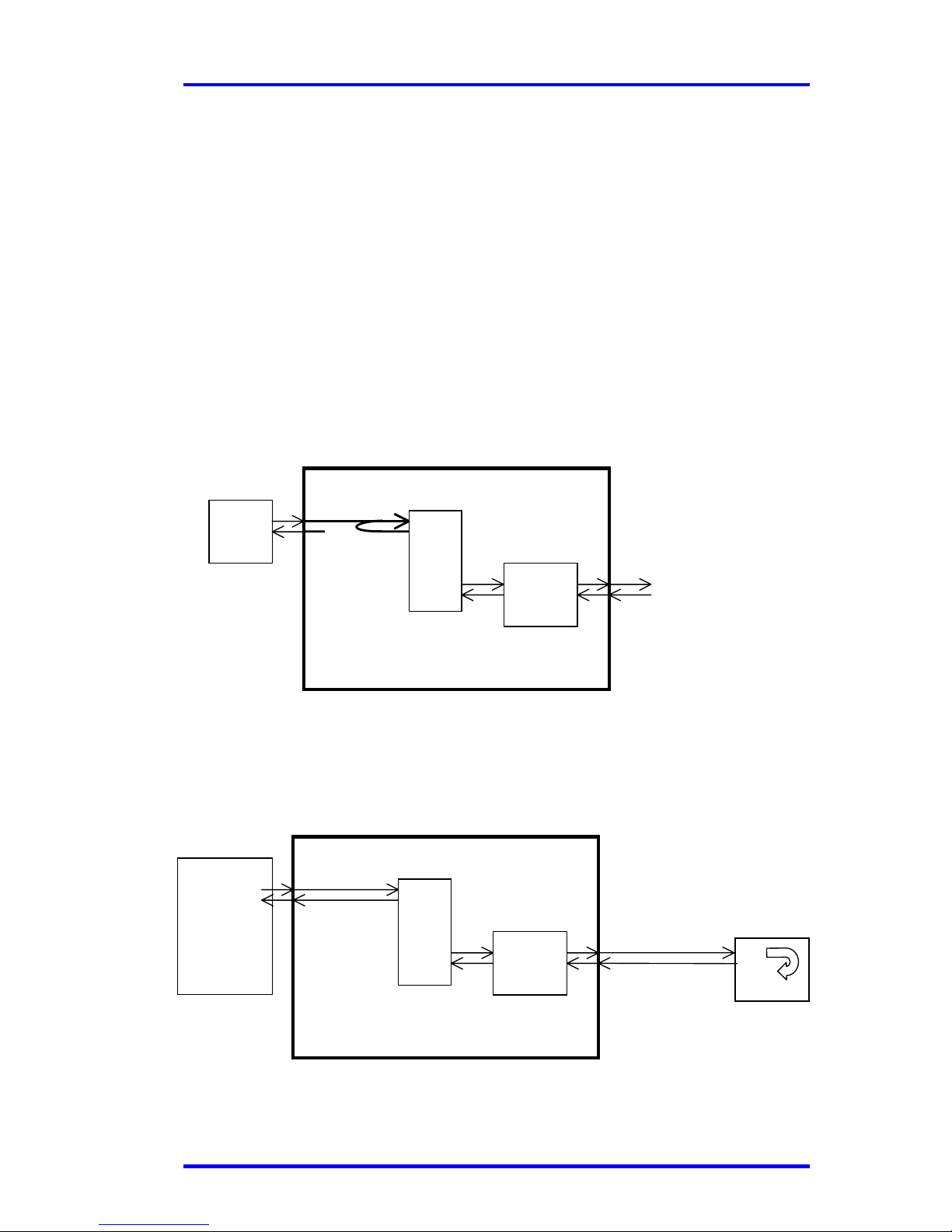
The example given here refers to use of CTC Union's BTM-10 T1
Transmission Analyzer. To test any of the FT1 Cards, connect either an RJ-45
T1 cable or two coaxial cables between the Device Under Test (DUT) and the
BTM-10 tester.
Configure the FT1 Card framed mode, B8ZS line code, termination (100
ohm, and internal clock source. Depress the front panel Loc dig loopbk switch.
Configure the analyzer for T1 BERT, unframed, 100 ohm termination, B8ZS
line code, external Tx and Rx clock, QRSS pattern and run "forever". Run the
BERT. Confirm 1.536Mbps rate and no receive errors. If testing a remote link,
inject a forced error and confirm loop back receipt of one error.
The BTM-10 may also be configured to do high-speed BERT from its
data port. Alternatively, our HCT-6000 or HCT-BERT 2M analyzers may be
configured to connect to the data port side of the DUT. In this setup, the FT1
Card and the link may be tested.
User
DTE
Data
Port
BTM-10
Analyzer
CSU
LOCAL FT1 Card
Datacom
tester
(BTM-10
or
HCT-6000)
Data
Port
CSU
LOCAL FT1 Card
T1
link
Remote
CSU/DSU
loop back
code sent
Page 34
Chapter 5. Troubleshooting
30 TRM-01 APR 2000
If for example the FT1 Card is an FT1/RS530, the tester is connected
directly to the RS-530 interface of the data port. The clock on the tester is set to
"external". Set up for BERT test and run a pattern to the data port. Depress the
Rem loopbk switch on the local unit. This will place the remote CSU into
loop back mode allowing the BERT signal to be received at the local unit. You
may run the BERT for a twenty-four hour period for a longevity test. It is
always a good idea to manually inject an error and confirm proper receipt of the
error from the link.
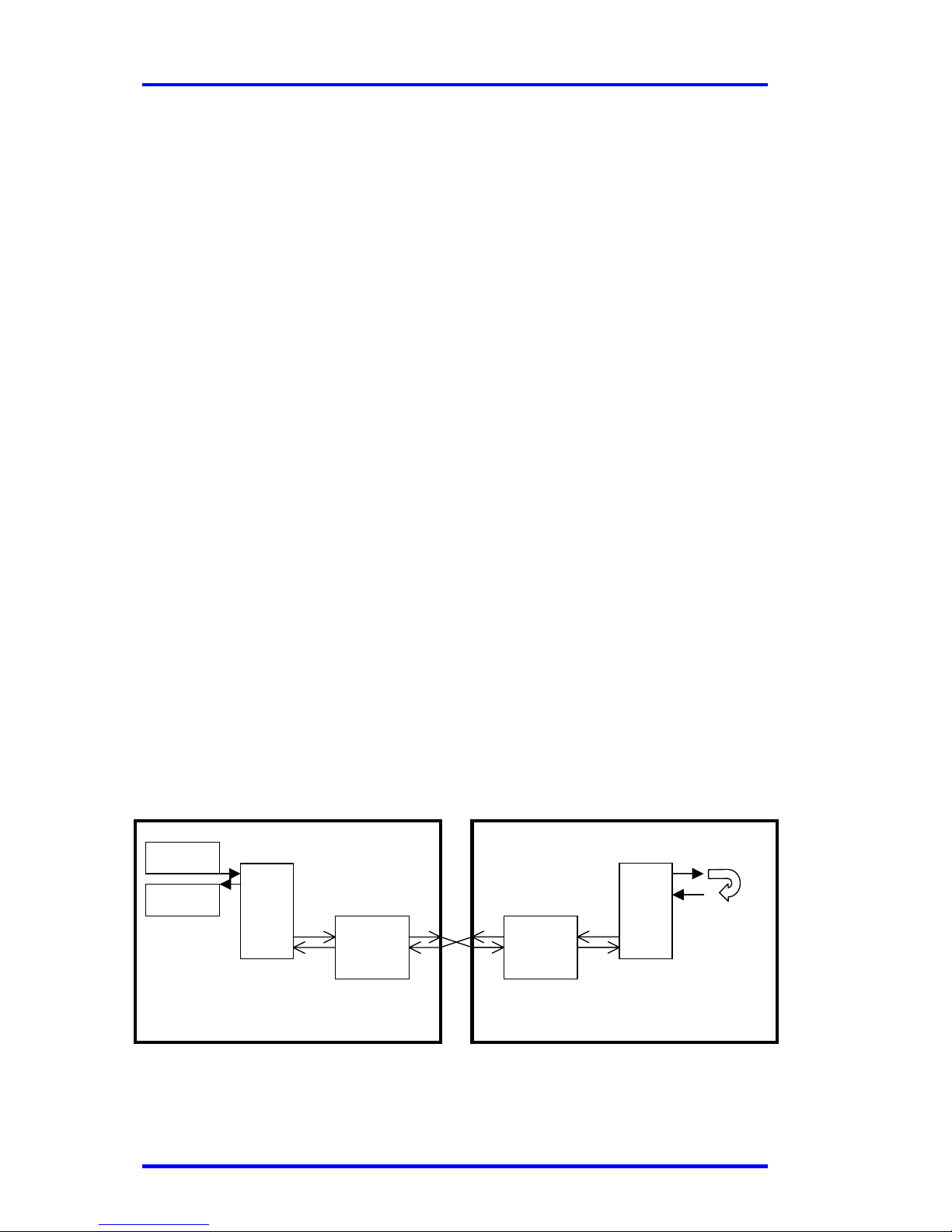
To test the FT1 Card standalone in the rack, the on-card pattern generator
and local loop back functions may be used without any external equipment.
Ensure that the FT1 Card has its clock source set to internal. Depress both the
Pattern and Loc ana loopback switches. The pattern generator is internally
connected to the DSU side while the loop back is placed on the CSU in analog
mode. (Refer to Figure 4-4 on page 25) The red Test LED will be lit and there
should be no Err LED indications. The yellow RD LED will flash since the
pattern generator is connected, running, and looping back to the DTE. The T1
link will experience Sig Loss, since it is not connected.
To test a pair of FT1 Cards in a rack, cross connect the T1 lines (Rx to
Tx, Tx to Rx), configure both cards for framed mode, and time slots 1 ~ 24 all
active. Set one card with internal clock source and the other for recovery. On
one card depress both the Pattern and Rem loopbk switches. Alternatively, on
one card depress the Pattern switch while depressing the Loc dig loopbk switch
on the other card. During successful loop back, both cards will exhibit flashing
yellow RD LEDs, and no red LED indications except Test.
Data
Port
CSU
LOCAL FT1 Card
Generator
Tester
CSU
Data
Port
LOCAL FT1 Card
Page 35
Chapter 5. Troubleshooting
31 TRM-01 APR 2000
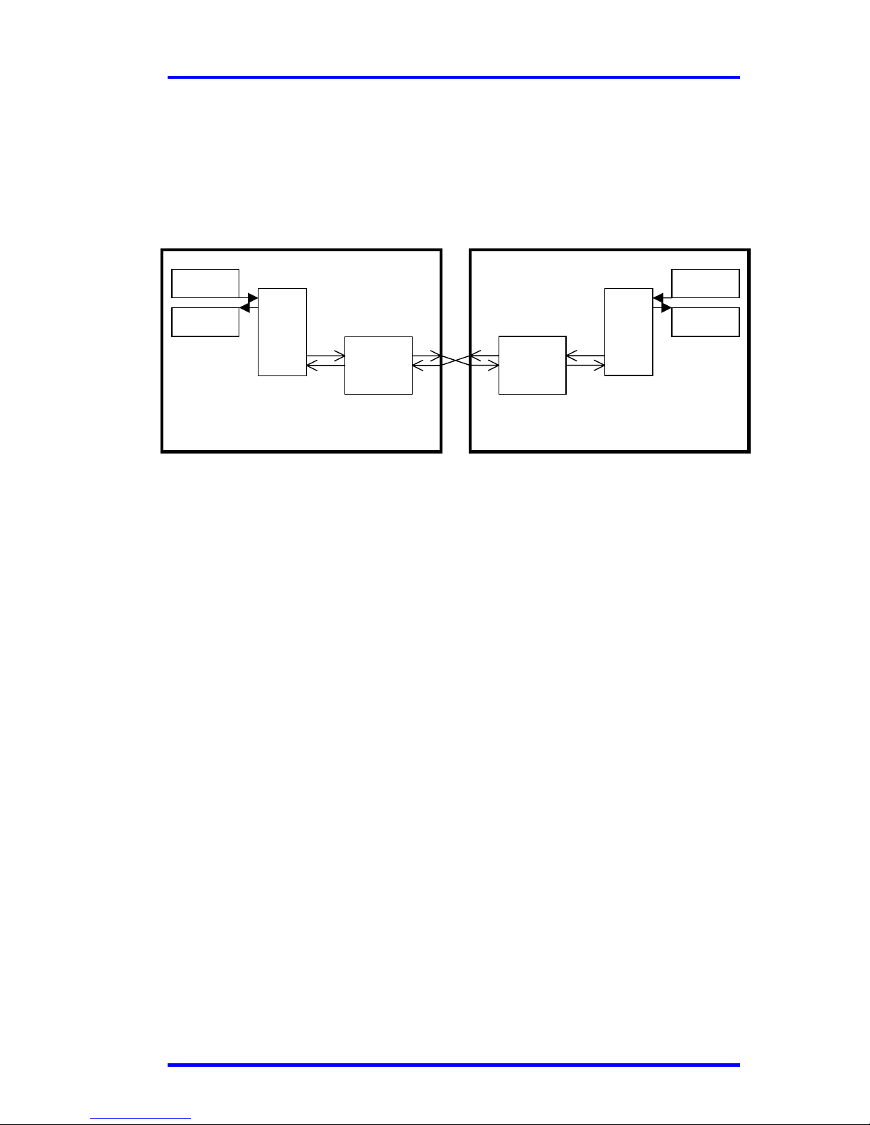
Here's one more test based upon the previous setup. Depress both Pattern
switches on each card. Now, each pattern generator is sending to the other card,
while each pattern tester is receiving the 511-bit pattern from the other card.
The same successful indicators as previous apply.
Data
Port
CSU
LOCAL FT1 Card
Generator
Tester
CSU
Data
Port
Generator
Tester
LOCAL FT1 Card
Page 36

Chapter 5. Troubleshooting
32 TRM-01 APR 2000
This page left blank intentionally.
Page 37
Appendix A. DIP Switch Settings
33 TRM-01 APR 2000
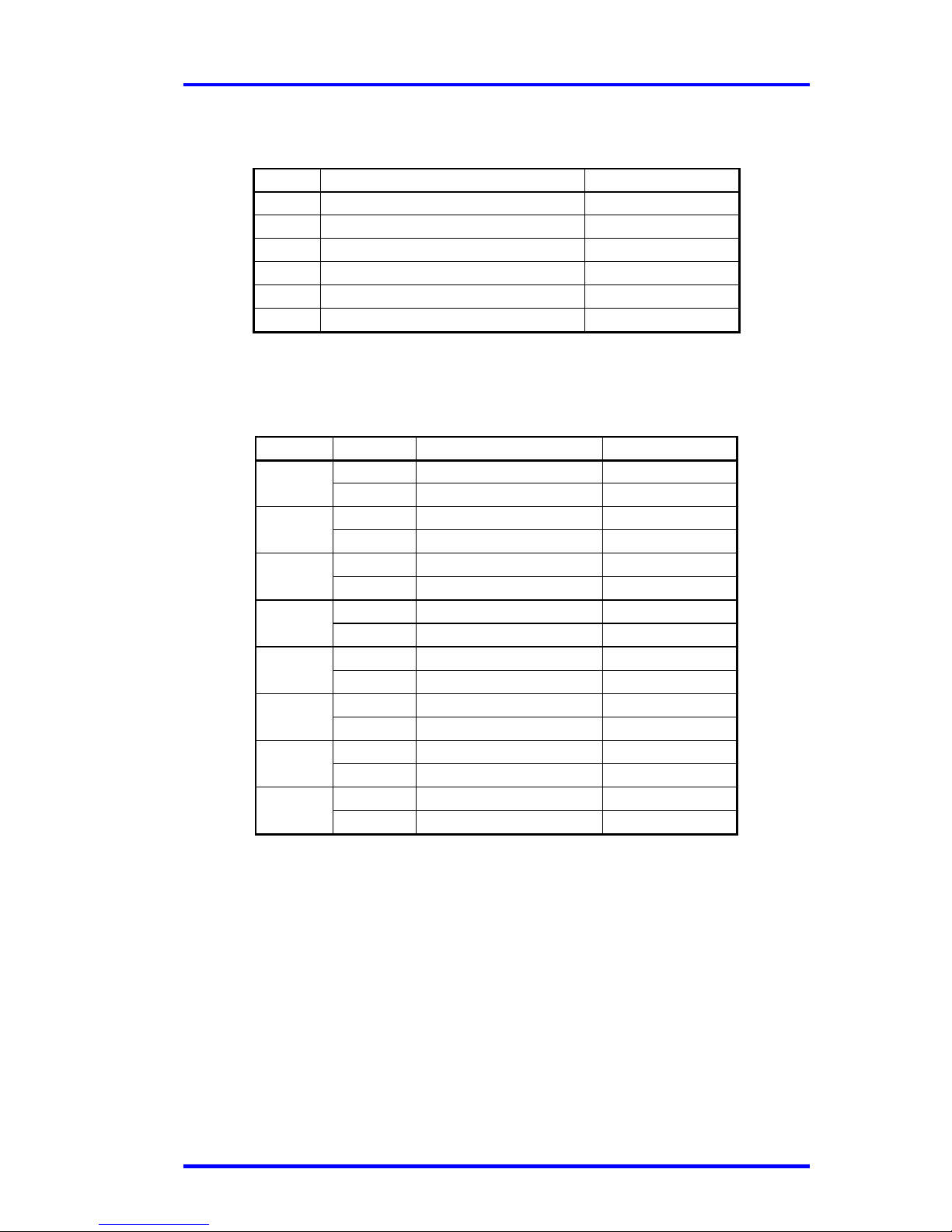
DIP SWITCH FUNCTION DESCRIPTIONS
DIPSW FUNCTION COMMENT
2 Time slot 1 to 8 settin
g
See Table A-2
3 Time slot 9 to 16 setting See Table A-3
4 Time slot 17 to 24 setting See Table A-4
5 Line build out setting See Table A-5
6 Parameter group 1 setting See Table A-6
7 Parameter group 2 setting See Table A-7
Table A-1 : DIP SWITCH FUNCTION DESCRIPTIONS
DIPSW2
DIP SW2 STATE FUNCTION COMMENT
-1 OFF Time slot 1 disable Note 1
ON Time slot 1 enable Note 2
-2 OFF Time slot 2 disable
ON Time slot 2 enable
-3 OFF Time slot 3 disable
ON Time slot 3 enable
-4 OFF Time slot 4 disable
ON Time slot 4 enable
-5 OFF Time slot 5 disable
ON Time slot 5 enable
-6 OFF Time slot 6 disable
ON Time slot 6 enable
-7 OFF Time slot 7 disable
ON Time slot 7 enable
-8 OFF Time slot 8 disable
ON Time slot 8 enable
Table A-2 : DIPSW2 TIME SLOT 1 TO 8 SETTING
Page 38
Appendix A. DIP Switch Settings
34 TRM-01 APR 2000
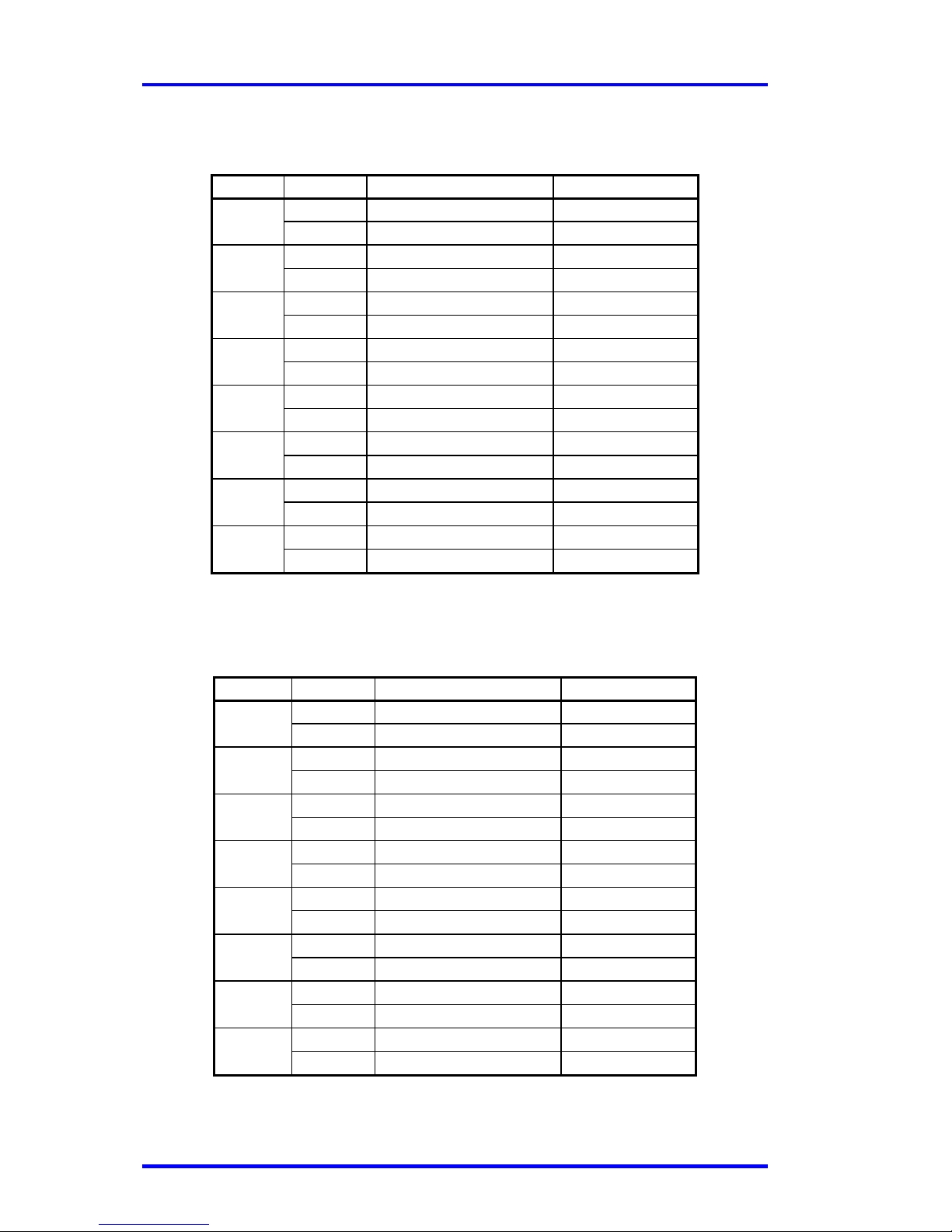
DIPSW3
DIP SW3 STATE FUNCTION COMMENT
-1 OFF Time slot 9 disable
ON Time slot 9 enable
-2 OFF Time slot 10 disable
ON Time slot 10 enable
-3 OFF Time slot 11 disable
ON Time slot 11 enable
-4 OFF Time slot 12 disable
ON Time slot 12 enable
-5 OFF Time slot 13 disable
ON Time slot 13 enable
-6 OFF Time slot 14 disable
ON Time slot 14 enable
-7 OFF Time slot 15 disable
ON Time slot 15 enable
-8 OFF Time slot 16 disable
ON Time slot 16 enable
Table A-3 : DIPSW3 TIME SLOT 9 TO 16 SETTING
DIPSW4
DIP SW4 STATE FUNCTION COMMENT
-1 OFF Time slot 17 disable
ON Time slot 17 enable Note 1
-2 OFF Time slot 18 disable
ON Time slot 18 enable
-3 OFF Time slot 19 disable
ON Time slot 19 enable
-4 OFF Time slot 20 disable
ON Time slot 20 enable
-5 OFF Time slot 21 disable
ON Time slot 21 enable
-6 OFF Time slot 22 disable
ON Time slot 22 enable
-7 OFF Time slot 23 disable
ON Time slot 23 enable
-8 OFF Time slot 24 disable
ON Time slot 24 enable
Table A-4 DIPSW4 TIME SLOT 17 TO 24 SETTING
Page 39
Appendix A. DIP Switch Settings
35 TRM-01 APR 2000
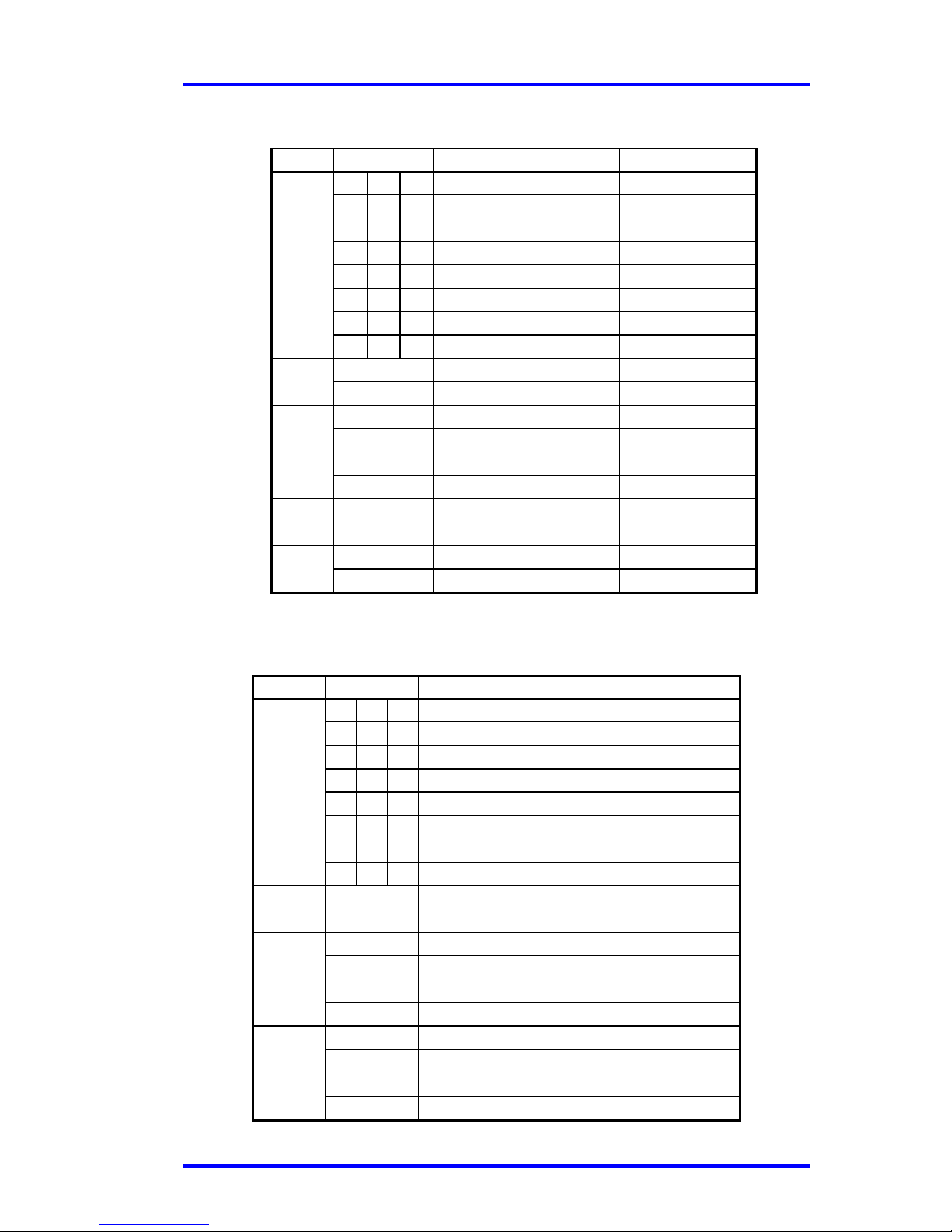
DIPSW5
DIP SW4
STATE FUNCTION COMMAND
-1,-2,-3
OFF OFF OFF
0 to 133 feet / 0dB
ON OFF OFF
133 to 266 feet
OFF ON OFF
266 to 399 feet
ON ON OFF
399 to 533 feet
OFF OFF ON
533 to 655 feet
ON OFF ON
-7.5 dB
OFF ON ON
-15 dB
ON ON ON
-22.5 dB
-4 OFF Reserved
ON Reserved
-5 OFF Reserved
ON Reserved
-6 OFF Reserved
ON Reserved
-7 OFF Reserved
ON Reserved
-8 OFF Reserved
ON Reserved
Table A-7 : DIPSW5 SETTING
DIPSW6
DIP SW6 STATE FUNCTION COMMENT
-1,-2,-3 OFF OFF OFF Clock mode 0
(
DCE1) Recover
y
1
ON OFF OFF Clock mode 1 (DCE2) Internal Osc.
1
OFF ON OFF Clock mode 2 (DTE1) Transparent
1
ON ON OFF Clock mode 3 (DTE2) Data Port
1
OFF OFF ON Clock mode 4 (DTE3) Data Port
1
ON OFF ON Reserve
OFF ON ON Reserve
ON ON ON Reserve
-4 OFF Line code: HDB3
ON Line code: AMI
-5 OFF Frame mode: CCS (PCM31) ignored when unframed
ON Frame mode: CAS (PCM30) ignored when unframed
-6 OFF CRC4: OFF ignored when unframed
ON CRC4: ON ignored when unframed
-7 OFF Idle code: Mark (0xff) ignored when unframed
ON Idle code: Flag (0x7e) ignored when unframed
-8 OFF Data channel rate: n × 64K ignored when unframed
ON Data channel rate: n × 56K ignored when unframed
Table A-8 : DIPSW6 PARAMETER GROUP 1 SETTING
Note 1: See Table A-10 for detailed clock mode.
Page 40
Appendix A. DIP Switch Settings
36 TRM-01 APR 2000
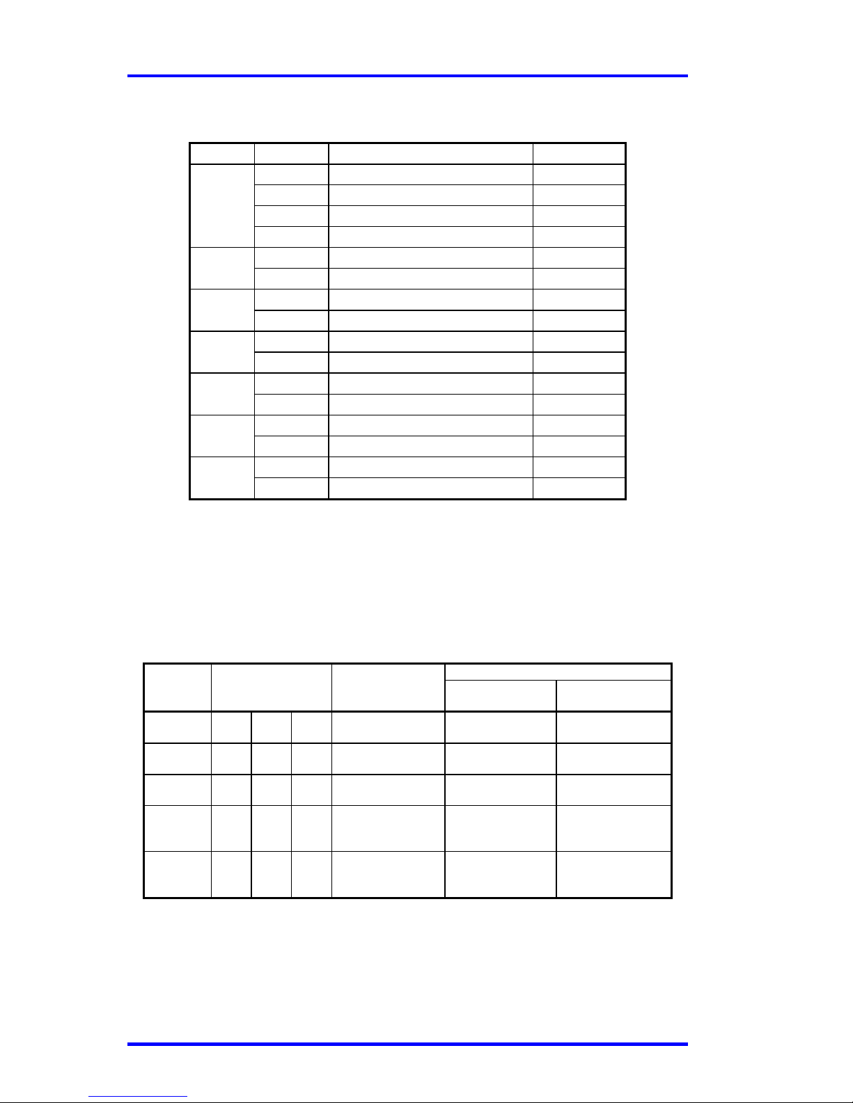
DIPSW7
DIP SW7 STATE FUNCTION COMMENT
-1 OFF RC timin
g p
olarity : Normal
ON RC timing polarity : Invert
-2 OFF TC timing polarity : Normal
ON TC timing polarity : Invert
-3 OFF DCD control : Always ON
ON DCD control : Follow RTS
-4 OFF Multiple (cascade) : Disable
ON Multiple (cascade) : Enable
-5 OFF Signaling : Non pass through
ON Signaling : Pass through
-6 OFF Setting from : DIP switch
ON Setting from : EEPROM
-7 OFF Data port controlled loopback: Disable
ON Data port controlled loopback: Enable
-8 OFF Front panel loopback: Disable Note 3
ON Front panel loopback: Enable
Table A-7 : DIPSW7 PARAMETER GROUP 2 SETTING
Note 1: Use this setting to de-activate the front panel pushbuttons. This will prevent unauthorized or accidental link breakage. In order for the front panel switches to function,
this setting must be ON. By default, it is ON from the factory.
CLOCK MODE DESCRIPTION
CLOCK DIPSW 6 T1 LINE USER DATA PORT
MODE STATE TRANSMIT RECEIVE TRANSMIT
-1 -2 -3 CLOCK SOURCE CLOCK SOURCE CLOCK SOURCE
0*
(DCT1)
OFF* OFF* OFF*
RECOVERY
RECOVERY
Output to RC pin
RECOVERY
Output to TC pin
1
(DCE2)
ON OFF OFF
INTERNAL
OSCILLATOR
INTERNAL
Output to RC pin
INTERNAL
Output to TC pin
2
(DTT1)
OFF ON OFF
EXTERNAL
Locked to ETC pin
RECOVERY
Output to RC pin
EXTERNAL
Input from ETC pin
3
(DTE2)
ON ON OFF
EXTERNAL
Locked to ETC pin
EXTERNAL
Input from DTR
pin
EXTERNAL
Input from ETC pin
4
(DTE3)
OFF OFF ON
EXTERNAL
Locked to ETC pin
EXTERNAL
Input from ETC
pin
EXTERNAL
Input from ETC pin
Table A-8 : CLOCK MODE DESCRIPTION
* This is the normal setting for network operation.
Page 41

Appendix A. DIP Switch Settings
37 TRM-01 APR 2000
This page left blank intentionally.
Page 42

notes:
38
Page 43

notes:
39
Page 44
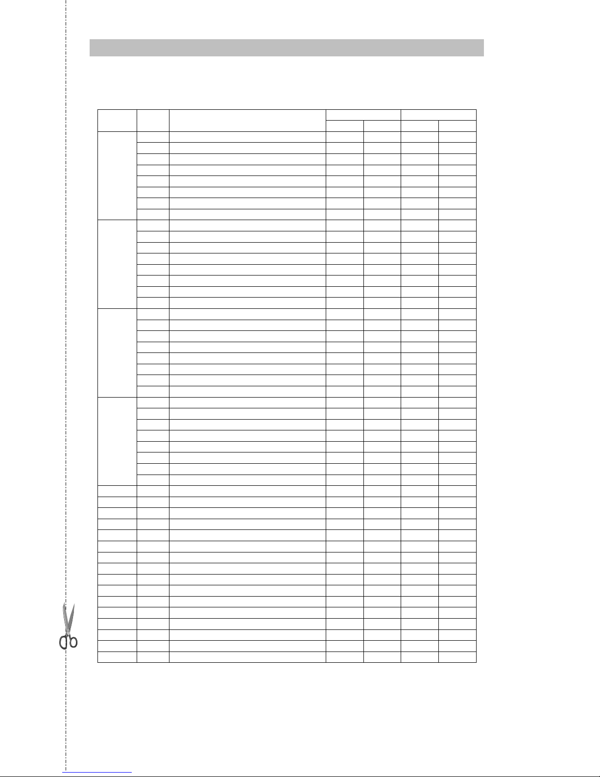
Technical Inquiry Form
TRM-01 MODEL No.: FT1/V.35 FT1/RS-530 FT1/ET10
Please fill in the DIP switches configuration with '✓' marks into the following
table. Send it to us by fax, and we will reply to you immediately.
Your Setting CTC Suggestion
SW NO. DIP
FUNCTION
ON OFF ON OFF
1 Timeslot 1
2 Timeslot 2
3 Timeslot 3
4 Timeslot 4
5 Timeslot 5
6 Timeslot 6
7 Timeslot 7
SW2
8 Timeslot 8
1 Timeslot 9
2 Timeslot 10
3 Timeslot 11
4 Timeslot 12
5 Timeslot 13
6 Timeslot 14
7 Timeslot 15
SW3
8 Timeslot 16
1 Timeslot 17
2 Timeslot 18
3 Timeslot 19
4 Timeslot 20
5 Timeslot 21
6 Timeslot 22
7 Timeslot 23
SW4
8 Timeslot 24
1 Line Build Out Setting
2 Line Build Out Setting
3 Line Build Out Setting
4 Reserved
5 Reserved
6 Reserved
7 Reserved
SW5
8 Reserved
SW6 1 Rx/Tx timing source
2 Rx/Tx timing source
3 Rx/Tx timing source
4 Line code: B8ZS or AMI
5 Frame mode : SF or ESF
6 Reserved
7 Idle code: Mark or Flag
8 Data port rate: n x 64K or n x 56K
SW7 1 RC Timing Polarity : Normal or Invert
2 TC Timing Polarity : Normal or Invert
3 DCD control : On or RTS
4 Cascade : Disable or Enable
5 Signaling : Non pass or pass through
6 Setting source : DIP SW or EEPROM
7 Data port loop back
8 Front panel switch functions
Page 45

Page 46

Page 47

Page 48

T1 Access Unit
CTC Union Technologies Co., Ltd.
Far Eastern Edison Science and Technologies Center
(Nei-Hu HI-TEC Park)
6F-3, Lane 360, Nei-Hu Road, Section 1
Nei-Hu, Taipei, Taiwan
Phone:(886) 2.2659.1021 (Rep) Fax:(886) 2.2799.1355
E-mail: [email protected]
http://www.ctcu.com
 Loading...