

Page 1
ST4761B01-3 Product Specification
MODEL: ST4761B01-3
Ver. 0.1
Date: 08.Mar.2013
Customer’s Approval
Signature Date
CSOT
Approved By Product Director
Name:Richard Lung
Signature:
Reviewed By PM Manager
Name:Aaron Tu
Signature:
Reviewed ByProject Leader
Name:Guanzheng lee
Signature:
Reviewed ByPM
Name:Yingnan Zou
Signature:
Date
Date
Date
Date
The copyright belongs to Shenzhen China Star 1 / 22Ver. 0.1
Optoelectronics Technology Co., Ltd.
Any unauthorized use is prohibited.
Page 2

ST4761B01-3 Product Specification
Contents
1. General Description ....................................................................................................................................... 4
1.1 Product Features .................................................................................................................................. 4
1.2 Overview .............................................................................................................................................. 4
1.3 General Information ............................................................................................................................. 4
2. Absolute Maximum Ratings .......................................................................................................................... 5
2.1 Absolute Maximum Ratings (TA = 25 ± 2 °C) .................................................................................... 5
2.2 Environment Requirement (Based on CSOT Module MT4761B01-1) ............................................... 5
2.3 Absolute Ratings of Environment (Open Cell) .................................................................................... 5
3. Electrical Specification .................................................................................................................................. 6
3.1 Open Cell Power Consumption (TA = 25 ± 2 °C) ............................................................................... 6
3.2 LVDS Characteristics ........................................................................................................................... 7
4. Input Terminal Pin Assignment ..................................................................................................................... 8
4.1 Interface Pin Assignment ..................................................................................................................... 8
4.2 Block Diagram of Interface ................................................................................................................. 9
4.3 LVDS Interface .................................................................................................................................. 10
4.3.1 NS Format (SELLVDS = H) ................................................................................................... 10
4.3.2 JEIDA Format (SELLVDS = L or Open) ................................................................................ 11
5. Interface Timing ........................................................................................................................................... 12
6. Optical Characteristics ................................................................................................................................. 14
6.1 Measurement Conditions ................................................................................................................... 14
6.2 Optical Specifications ........................................................................................................................ 15
7. Mechanical Characteristics .......................................................................................................................... 18
7.1 Mechanical Specification ................................................................................................................... 17
7.2 Packing............................................................................................................................................... 19
7.2.1 Packing Specifications ............................................................................................................ 19
7.2.2 Packing Method ...................................................................................................................... 19
8. Definition of Labels ..................................................................................................................................... 20
8.1 Open Cell Label ................................................................................................................................. 20
8.2 Carton Label ...................................................................................................................................... 21
8.3 Pallet Label ........................................................................................................................................ 21
9. Precautions ................................................................................................................................................... 22
9.1 Assembly and Handling Precautions ................................................................................................. 22
9.2 Safety Precautions.............................................................................................................................. 22
The copyright belongs to Shenzhen China Star 2 / 22Ver. 0.1
Optoelectronics Technology Co., Ltd.
Any unauthorized use is prohibited.
Page 3
ST4761B01-3 Product Specification
Revision History
Version Date Page (New) Section Description Revision by
Ver. 0.1 08.Mar..2013
All All
Tentative Specification was First Issued. Yingnan Zou
The copyright belongs to Shenzhen China Star 3 / 22Ver. 0.1
Optoelectronics Technology Co., Ltd.
Any unauthorized use is prohibited.
Page 4
1. General Description
Typical value measured at CSOT’s
ST4761B01-3 Product Specification
1.1 Product Features
- FHD Resolution (1920 x 1080)
- VeryHigh Contrast Ratio:4000:1
- Fast Response Time
- Ultra Wide Viewing Angle: 178° (H)/178° (V)(CR≥≥≥≥10)
- DE (Data Enable) Mode
- LVDS (Low Voltage Differential Signaling) Interface
1.2Overview
ST4761B01-3 is a diagonal47.6”color active matrix LCDopen cellwith2ch-LVDS interface. This open cellis a
transmissive type display operating in the normally black mode. It supports 1920x1080FHD resolution and can display up
to16.7M colors (8bit). Each pixel is divided into Red, Green and Blue sub-pixels which are arranged in vertical stripe.
This open celldedicates for LCD TV products and provides excellent performance which includes high transparency, ultra
wide viewing angleand high color depth. CSOT open cell comply with RoHS for identification.
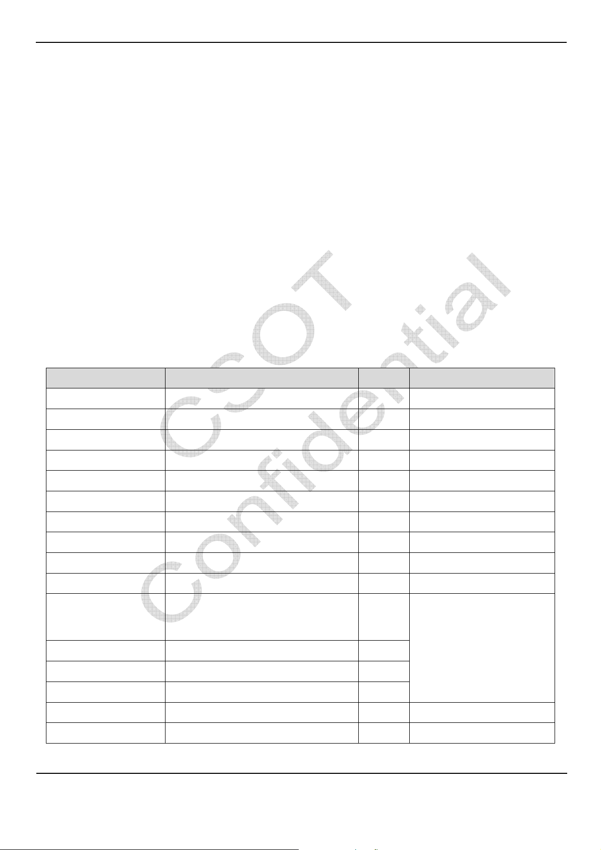
1.3 General Information
Item Specification Unit Note
Active Area 1054.08(H)x592.92(V) mm
Cell Size 1068.750(H) x 607.610 (V) x 1.750 (D) mm
Weight 1.9 kg Max.
Driving Scheme a-Si TFT Active Matrix -
Number of Pixels 1920x1080 pixel
Pixel Pitch (Sub Pixel) 0.183 (H) x 0.549 (V) mm
Pixel Arrangement RGB Vertical Stripe -
Display Colors 16.7 M color 8bit
Display Mode Transmissive Mode, Normally Black -
Glass Thickness (Array/CF) 0.5/0.5 mm
R=(0.639,0.335)
Color Chromaticity
G=(0.319,0.626)
B=(0.155,0.052)
W=(0.280,0.290)
Contrast Ratio 4000:1(Typ.)
module: MT4761B01-1
Cell Transmittance 5.65% (Typ.) %
View Angle(CR>10) +89/-89(H),+89/-89(V) (Typ.)
Polarizer(CF side) Anti-glare, Haze2%, Hard Coating(3H)
Polarizer(TFT side) Hard Coating(3H)
The copyright belongs to Shenzhen China Star 4 / 22Ver. 0.1
Optoelectronics Technology Co., Ltd.
Any unauthorized use is prohibited.
Page 5
2.Absolute Maximum Ratings
2.1 AbsoluteMaximum Ratings (TA= 25 ± 2 °C)
The followings are maximum values which, if exceeded, may cause damage to the unit.
ST4761B01-3 Product Specification
Item Symbol
Min. Max.
Power Supply Voltage VCC -0.3 13.8 V
Input Signal Voltage VIN -0.3 4.0 V
Value
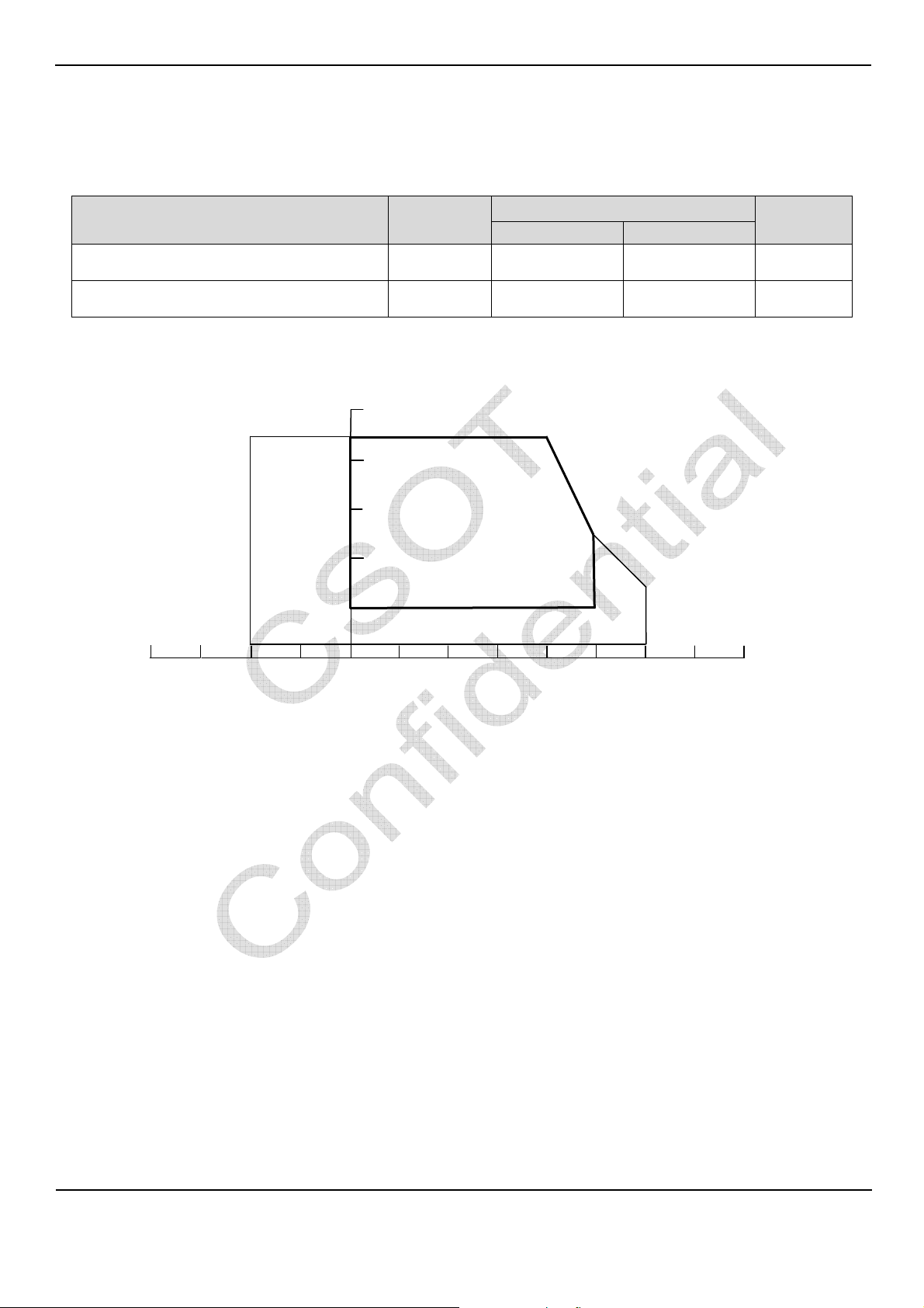
2.2 Environment Requirement (BasedonCSOT ModuleMT4761B01-1)
(1) Temperature and relative humidity range are shown as below.
Relative Humidity (%RH)
100
39ºC,90%
80
60
Operating Range
40
-40
-20
20
0
Storage Range
20
40
60
Temperature (ºC)
80
Unit
Fig. 2.1Operating and storage environment
(a) 90%RH maximum (TA≤39 ºC).
(b) Wet-bulb temperature should be 39ºCmaximum (TA>39 ºC).
(c) No condensation.
(2) The storage temperature is between - 20 ºCto 60 ºC,and the operating ambient temperature is between 0 ºC to 50 ºC.
The maximum operating temperature is based on the testcondition that the surface temperature of display area is less than
or equalto 65ºC with LCD module in a temperature controlled chamber alone. Thermalmanagement should be considered
in final product design to prevent the surfacetemperature of display area from being over 65ºC. The range of operating
temperature may degrade in case of improper thermal management in the end product design.
(3) The rating of environment is based on LCD module. Leave LCD cell alone, this environment conditioncan’t be guaranteed.
Except LCD cell, the customer has to consider the ability of other parts of LCDmodule and LCD module process.
2.3 AbsoluteRatings of Environment (Open Cell)
When storing open cell as spares for a long time,please follow the precaution instructions:
(1) Do not store the module in high temperatureand high humidity for a long time. It is highly recommended to store the
module with temperature from20ºC to 30ºCin normal humidity (50±10%RH) with shipping package.
(2)The open cell should be keep within one month shelf life
The copyright belongs to Shenzhen China Star 5 / 22Ver. 0.1
Optoelectronics Technology Co., Ltd.
Any unauthorized use is prohibited.
Page 6
Shenzhen China Star
3.Electrical Specification
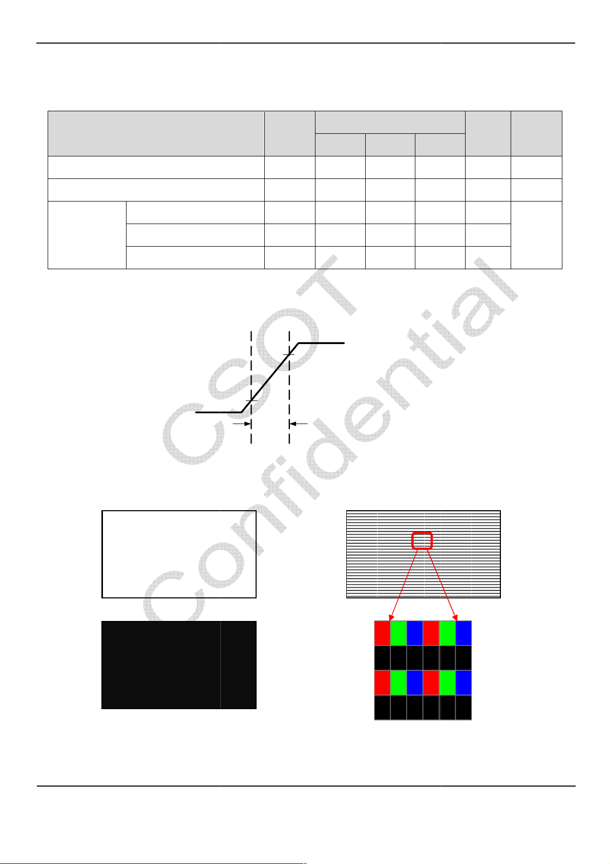
Consumption (TA = 25 ± 2 °C)
The ripple voltage should be controlled
rising time
3
= 25 ± 2ºC,
White Pattern B
CC
ST4761B01
Max.
13.2
2.0
0.49
1.01
0.44
shown as below.
B B R
R
R
R
G
G
R
R
R
R
G
G
B
B
B B G
G
B
G
G
B
-3 Product Specification
3.1 Open Cell Power
Parameter
Power Supply Voltage
Rush Current
White Pattern
Power Supply
Horizontal Stripe
Current
Black Pattern
Note:
(1)
(2)Measurement condition: V
CC=
12V
GND
less than10%ofVCC.
V
=470μs.
x 0.1
Symbol
Min.
VCC 10.8 12.0
I
- -
RUSH
ICC -
ICC -
ICC -
VCCx 0.9
470μs
VCC
Value
Typ.
0.38
0.78
0.34
Unit Note
V (1)
A (2)
A
A
A
(3)
(3)Measurement condition:VCC=12V, Ta
A.
C. Black Pattern
Fig. 3.2 Test patterns
Fig.
.1 VCC rising time condition
F = 60 Hz. The test patterns are
. Horizontal Pattern
The copyright belongs to
Optoelectronics Technology Co., Ltd.
Any unauthorized use is prohibited.
6 / 22Ver. 0.1
Page 7
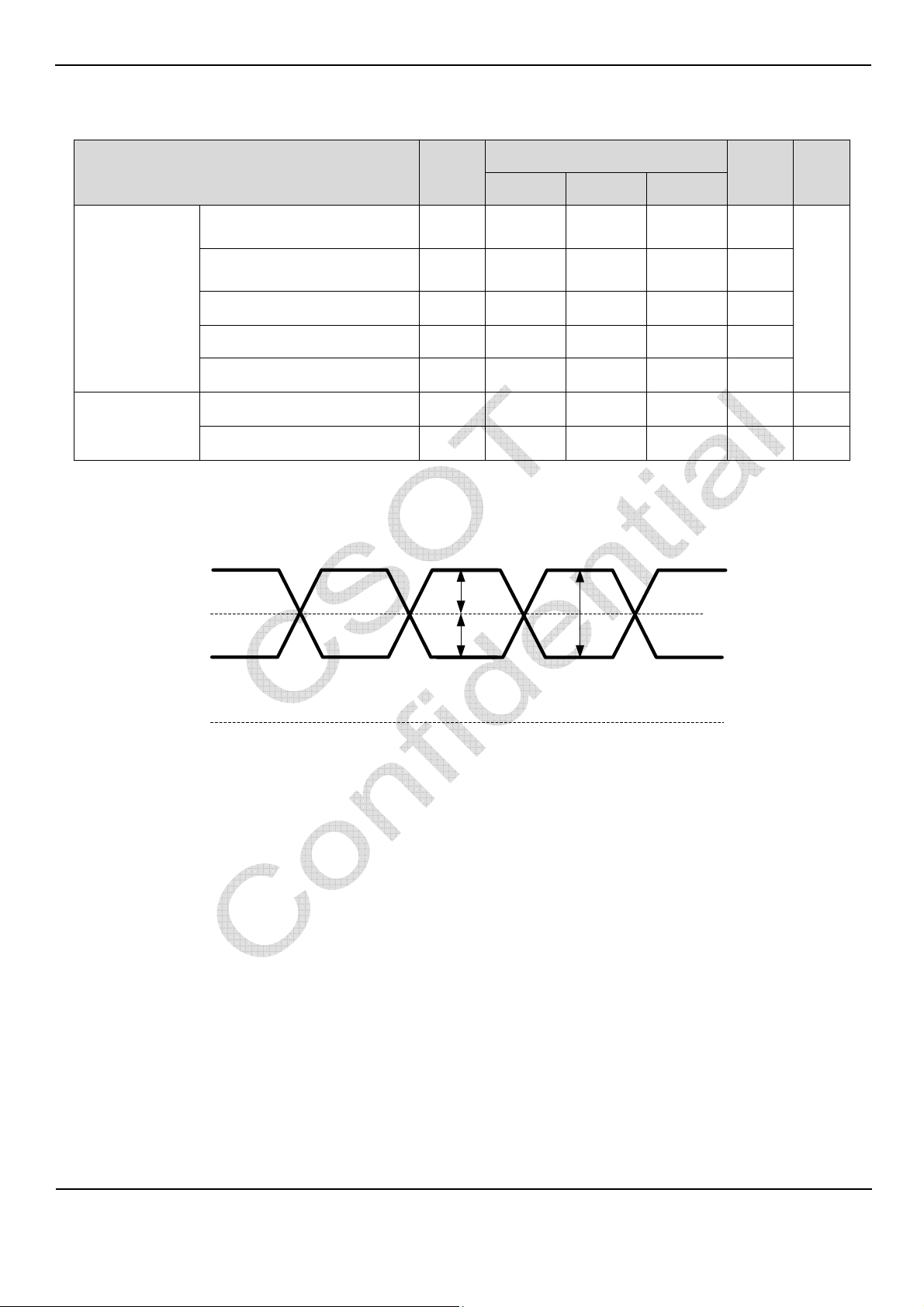
3.2 LVDS Characteristics
Parameter
Symbol
ST4761B01-3 Product Specification
Value
Unit Note
Min. Typ. Max.
Differential Input High
Threshold Voltage
Differential Input Low
Threshold Voltage
LVDS Interface
Common InputVoltage VCM 1.0 1.2 1.4 V
Differential Input Voltage |VID| 200 400 600 mV
Terminating Resistor RT 87.5 100 112.5 ohm
Input High ThresholdVoltage VIH 2.7 - 3.3 V
CMOSInterface
Input Low Threshold Voltage VIL 0 - 0.7 V
Note:
(1) The LVDS input signal has been defined as follows:
VCM
VTH +100 - - mV
VTL - - -100 mV
VTH
|VID|
VTL
(1)
GND
Fig. 3.3 LVDS input signal
The copyright belongs to Shenzhen China Star 7 / 22Ver. 0.1
Optoelectronics Technology Co., Ltd.
Any unauthorized use is prohibited.
Page 8
4.Input Terminal Pin Assignment
ST4761B01-3 Product Specification
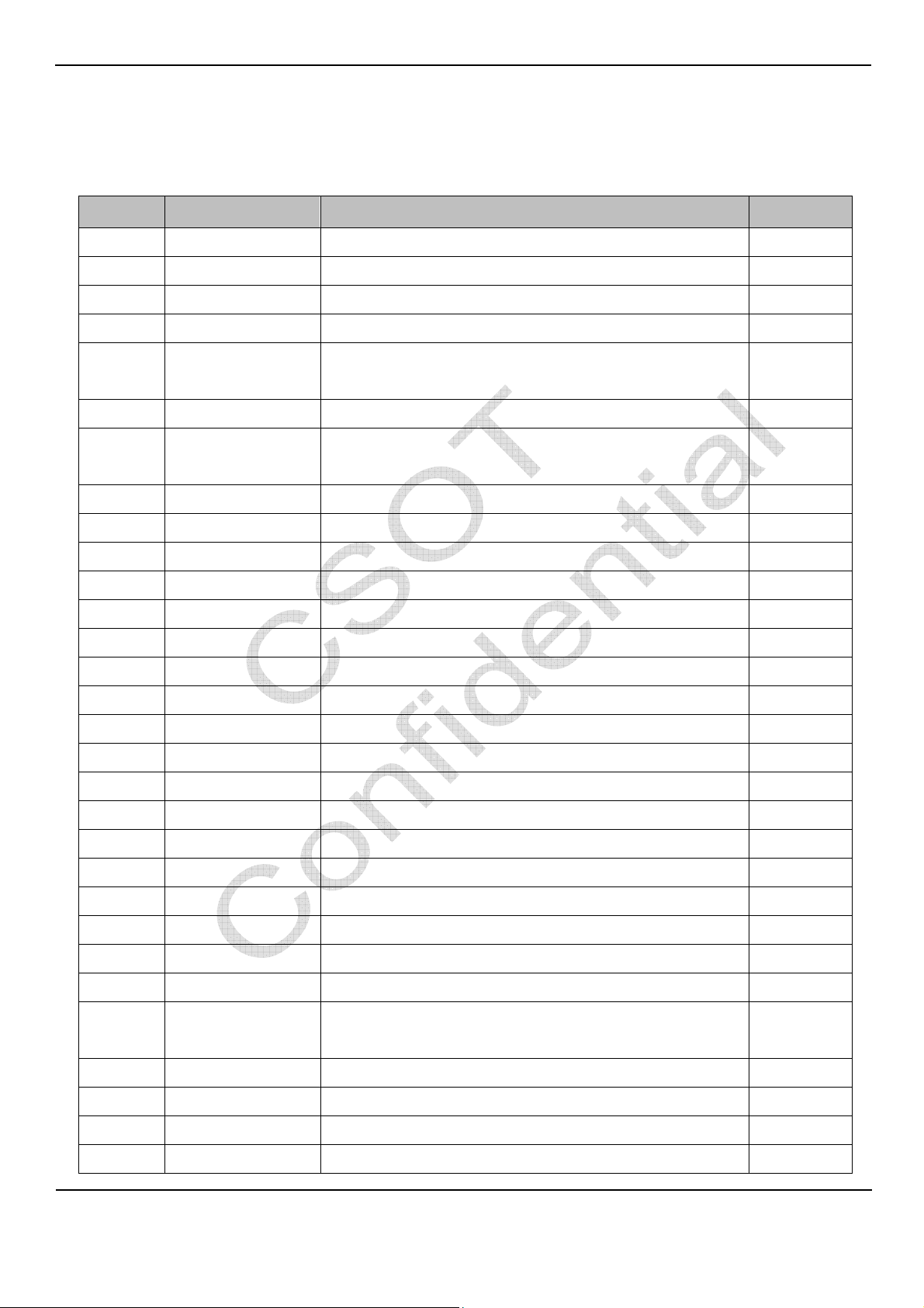
4.1 Interface Pin Assignment
CN1: CT000041-513C (FCN)or equivalent(see Note (1))
Pin No.
Symbol Description Note
1 N.C No Connection (1)
2 SCL I2C Serial Clock (for 3D Format Selection Function)
3 SDA I2C Serial Data (for 3D Format Selection Function)
4 N.C No Connection (1)
Output Signal for Left Right Glasses Control
5 L/R_O
(High: Left Glass turn onLow:Right glass turn on)
6 N.C. No Connection
Input Signal for LVDS Data Format Selection
7 SELLVDS
(High:VESA Format,Low or Open JEIDA Format)
8 N.C. No Connection (1)
9 N.C. No Connection (1)
10 N.C. No Connection (1)
11 GND Ground
(2)
12 ORX0- Odd Pixel Negative LVDS Differential Data Input. Channel 0
13 ORX0+ Odd Pixel Positive LVDS Differential Data Input. Channel 0
14 ORX1- Odd Pixel Negative LVDS Differential Data Input. Channel 1
15 ORX1+ Odd Pixel Positive LVDS Differential Data Input. Channel 1
16 ORX2- Odd Pixel Negative LVDS Differential Data Input. Channel 2
17 ORX2+ Odd Pixel Positive LVDS Differential Data Input. Channel 2
18 GND Ground
19 OCLK- Odd Pixel Negative LVDS Differential Clock Input
20 OCLK+ Odd Pixel Positive LVDS Differential Clock Input
21 GND Ground
22 ORX3- Odd Pixel Negative LVDS Differential Data Input. Channel 3
23 ORX3+ Odd Pixel Positive LVDS Differential Data Input. Channel 3
24 N.C. No Connection (1)
25 N.C. No Connection (1)
Input Signal for 2D/3D Mode Selection
26 2D/3D
(High:3D Enable,LOW:3D Disable)
27 N.C. No Connection (1)
28 ERX0- Even Pixel Negative LVDS Differential Data Input. Channel 0
29 ERX0+ Even pixel Positive LVDS Differential Data Input. Channel 0
30 ERX1- Even Pixel Negative LVDS Differential Data Input. Channel 1
The copyright belongs to Shenzhen China Star 8 / 22Ver. 0.1
Optoelectronics Technology Co., Ltd.
Any unauthorized use is prohibited.
Page 9
ST4761B01-3 Product Specification
CN1
31 ERX1+ Even Pixel Positive LVDS Differential Data Input. Channel 1
32 ERX2- Even Pixel Negative LVDS Differential Data Input. Channel 2
33 ERX2+ Even Pixel Positive LVDS Differential Data Input. Channel 2
34 GND Ground
35 ECLK- Even Pixel Negative LVDS Differential Clock Input
36 ECLK+ Even Pixel Negative LVDS Differential Clock Input
37 GND Ground
38 ERX3- Even Pixel Negative LVDS Differential Data Input. Channel 3
39 ERX3+ Even Pixel Positive LVDS Differential Data Input. Channel 3
40 N.C. No Connection
41 N.C. No Connection
42 N.C. No Connection (1)
43 N.C. No Connection (1)
44 GND Ground
45 GND Ground
46 GND Ground
47 N.C. No Connection (1)
48 VCC +12V Power Supply
49 VCC +12V Power Supply
50 VCC +12V Power Supply
51 VCC +12V Power Supply
Note:
(1)For CSOT internal only,please let it open.
(2) High: connect to +3.3V
(3)The first LVDS data is ODD LVDS data
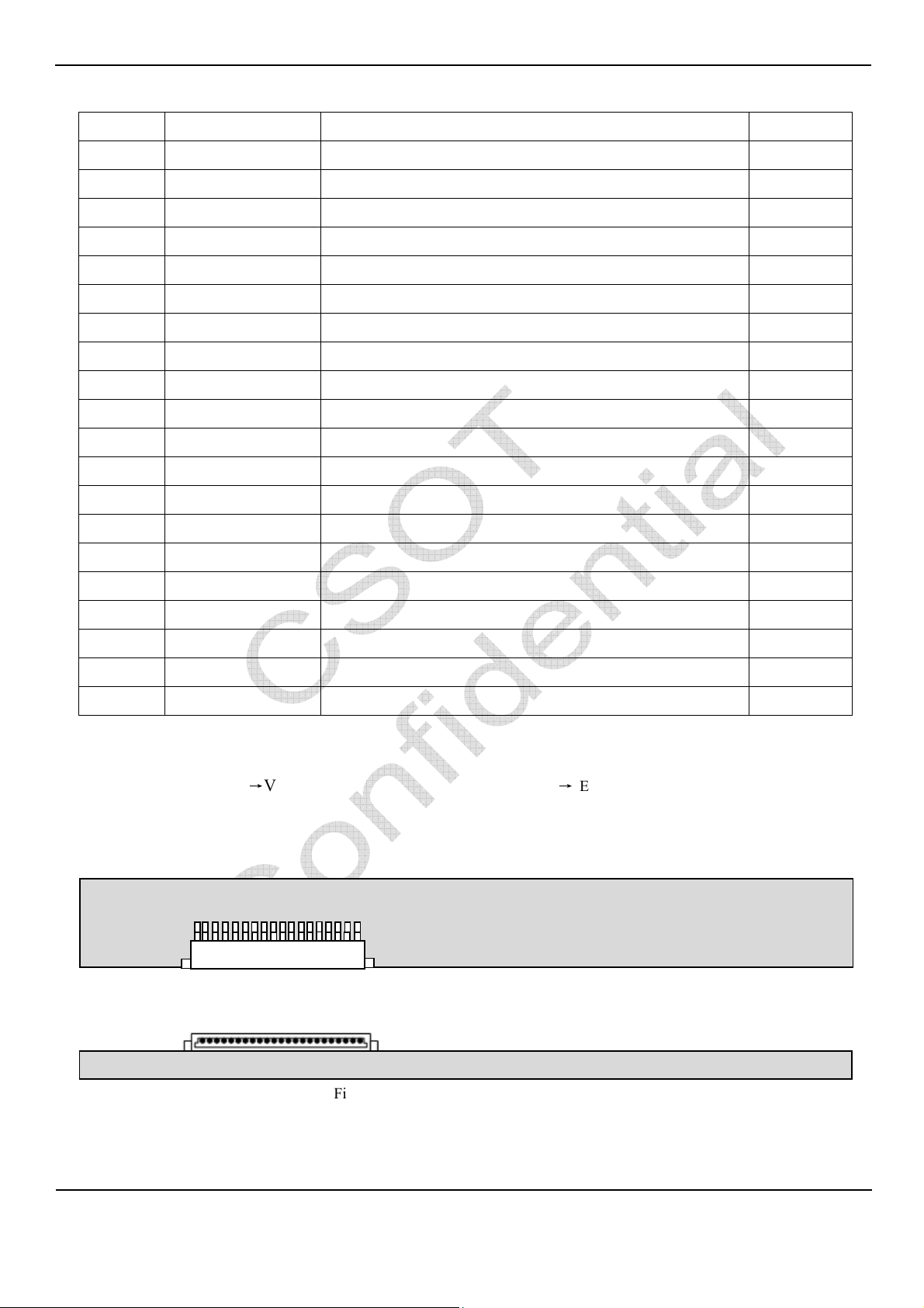
(4)The direction of pin assignment is shown as below:
→
VESA Format
;Low: connect to GND or Open→JEIDA format.
#1
#51
(1)
(2)
CN1
#1
(3)
The copyright belongs to Shenzhen China Star 9 / 22Ver. 0.1
Optoelectronics Technology Co., Ltd.
Any unauthorized use is prohibited.
#51
Fig. 4.1 LVDS connector direction sketch map
Page 10
Shenzhen China Star
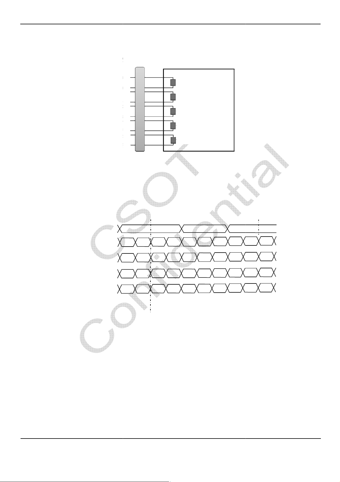
Block Diagram of Interface
resistor between positive and negative lines of each receiver input
ohms per signal line or about
Format (SELLVDS =
Connector
LV
CK1P
LV1N
3
LV1
P1
LV1N
2
LV1N0
LV1P0
L
V1N
1
LV1
P2
LV
CK1
N
LV1
P3
ST4761B01
pair line
Connector
3
100Ω
100Ω
100Ω
100Ω
100Ω
-3 Product Specification
4.2
Attention:
(1) Thisopen cell uses a 100 ohms (Ω)
(2) LVDS cable impedance shall be 50
4.3 LVDS Interface
4.3.1 VESA
Timing Controller
H)
100 ohms per twist-
.
respectively.
RCLK1P/ RCLK2P
RA1P/ RA2P
RB1P/ RB2P
RC1P/ RC2P
RD1P/ RD2P
G0 R5 R4R3R2R1R0
B1 B0G5 G4 G3G2G1
DE VS HS B5 B4B3B2
NAB7B6G7 G6R7R6
Fig. 4.2VESAformat
The copyright belongs to
Optoelectronics Technology Co., Ltd.
Any unauthorized use is prohibited.
10 / 22Ver. 0.1
Page 11
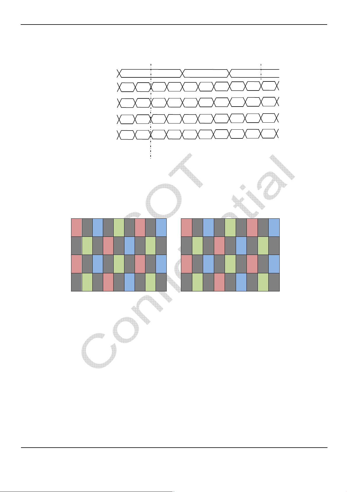
4.3.2 JEIDA Format (SELLVDS = L or Open)
RCLK1P / RCLK2P
ST4761B01-3 Product Specification
RA1P/ RA2P
RB1P/ RB2P
RC1P/ RC2P
RD1P/ RD2P
4.4Pattern FOR Vcom Adjustment
Dot - inversion pattern
Frame N Frame N+1
+
-
+
-
+
-
+
-
+
-
+
-
G2 R7 R6R5R4R3R2
B3 B2G7 G6 G5G4G3
DE VS HS B7 B6B5B4
NAB1B0G1 G0R1R0
Fig. 4.3 JEIDA format
+
-
+
-
+
-
-
+
-
+
-
+
-
+
-
+
-
+
-
+
-
+
-
+
+
-
+
-
+
-
+
-
+
-
+
-
+
-
+
-
+
-
-
+
-
+
-
+
-
+
-
+
-
+
-
+
-
+
-
+
The copyright belongs to Shenzhen China Star 11 / 22Ver. 0.1
Optoelectronics Technology Co., Ltd.
Any unauthorized use is prohibited.
Page 12
5.Interface Timing
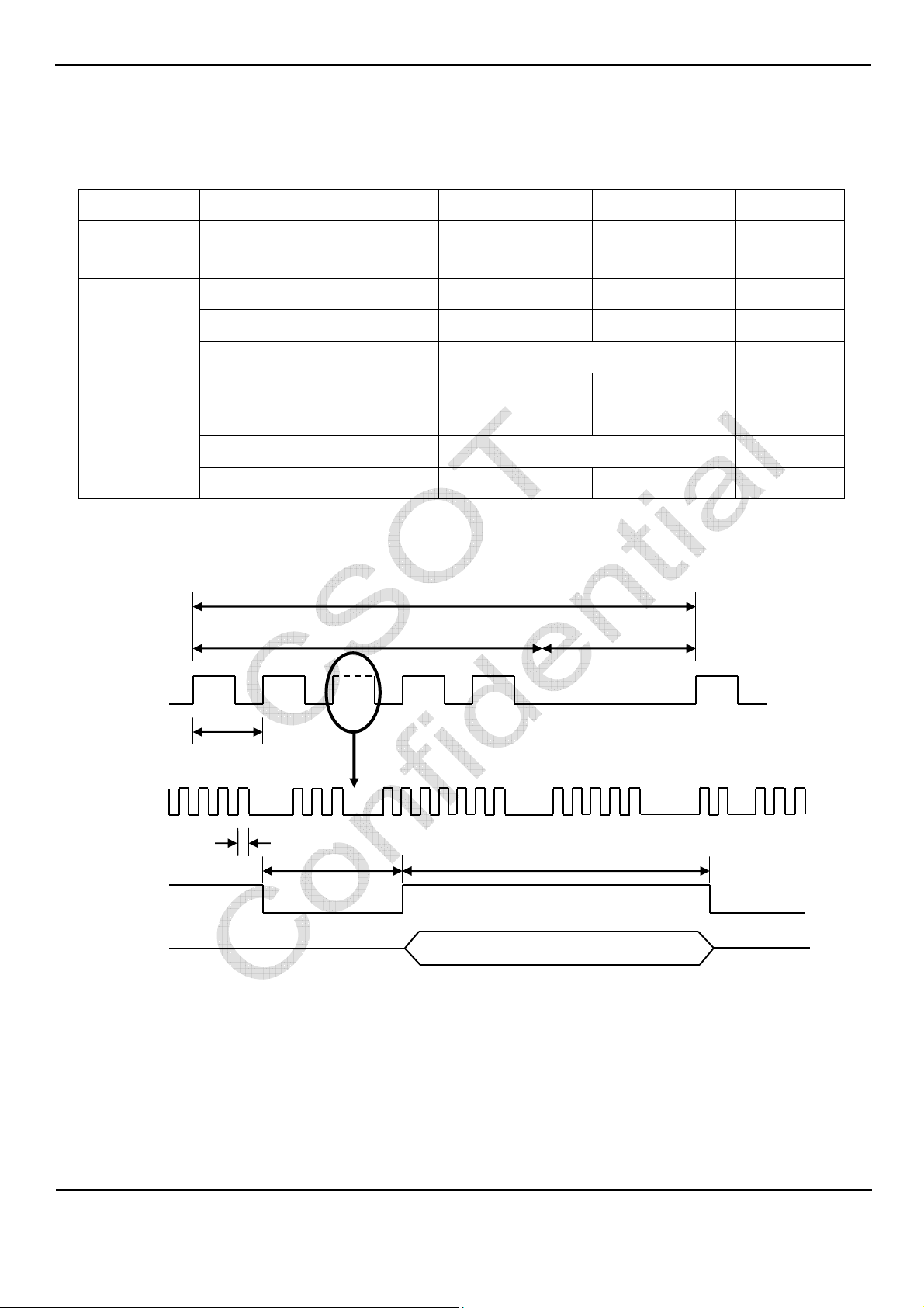
5.1 TimingTable (DE Only Mode)
Signal Item Symbol Min. Typ. Max. Unit Note
LVDSClock Frequency
Frame Rate F 57 60 62.5 Hz
F
(=1/T
CLK
CLK
ST4761B01-3 Product Specification
55.2 74.25 77.8 MHz
)
Vertical
Term
Horizontal
Term
Attention:
(1)The module is operated in DE only mode, Hsync and Vsync input signal have no effect on normal operation.
Total TV 1115 1125 1380 TH TV=TVD+TVB
Display TVD 1080
Blank TVB 35 45 300 TH
Total TH 1050 1100 1150 T
Display THD 960
Blank THB 90 140 190 T
TV
TVD TVB
TH=THD+THB
CLK
CLK
DE
TH
DCLK
DE
T
CLK
THB
DATA
ValidDisplay Data(960 clocks)
Fig. 5.1 Interface signal timingdiagram
The copyright belongs to Shenzhen China Star 12 / 22Ver. 0.1
Optoelectronics Technology Co., Ltd.
Any unauthorized use is prohibited.
THD
Page 13
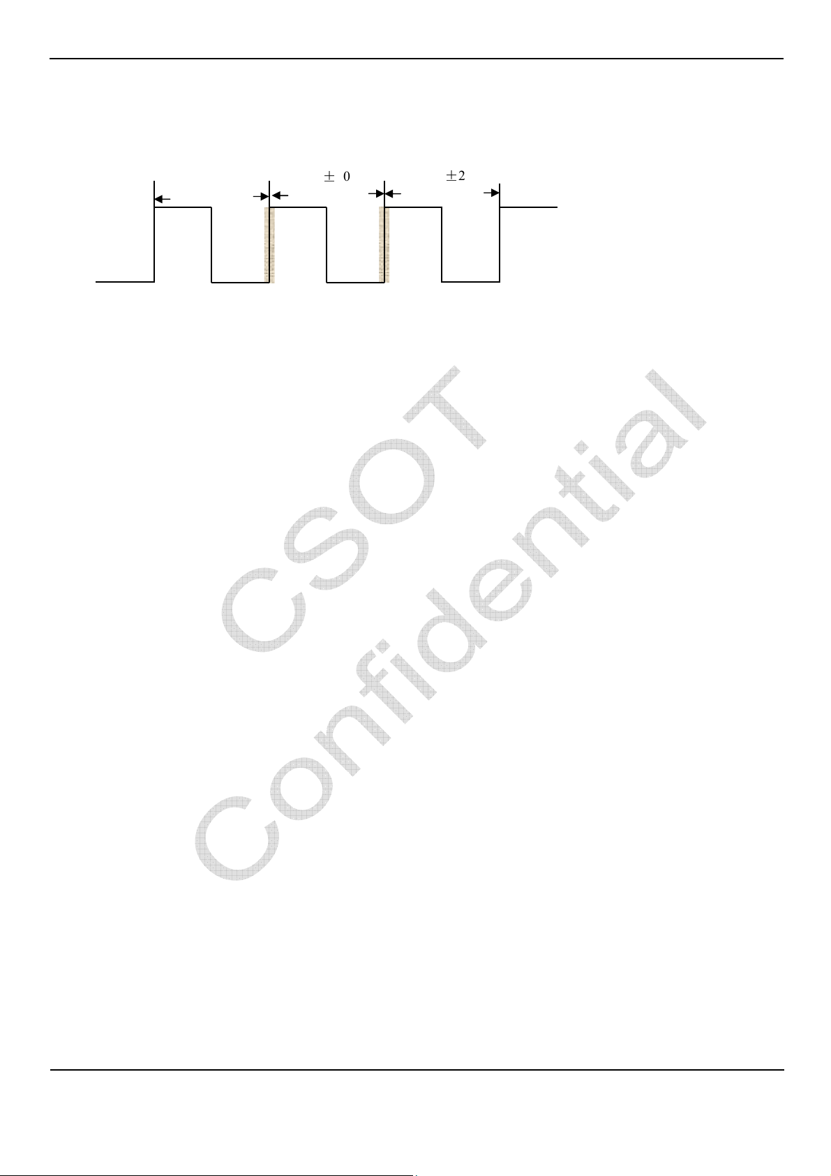
(2) The input clock cycle-to-cycle is defined as below figures.
T2=T1
200ps
T
T1=T±200ps
ST4761B01-3 Product Specification
±
Fig. 5.2 jitter
The copyright belongs to Shenzhen China Star 13 / 22Ver. 0.1
Optoelectronics Technology Co., Ltd.
Any unauthorized use is prohibited.
Page 14
6. Optical Characteristics
N =
S
A
6.1 Measurement Conditions
The tablebelow is the test condition of optical measurement.
Item Symbol Value Unit
ST4761B01-3 Product Specification
Ambient Temperature TA
Ambient Humidity HA
25±2
50±10
ºC
%RH
Supply Voltage VCC 12 V
Driving Signal Refer to the typical value inChapter 3: Electrical Specification
Vertical Refresh Rate FR 120 Hz
To avoid abrupt temperature change during optical measurement, it’s suggested to warm up the LCD module more than 60
minutes after lighting the backlight and in the windless environment.
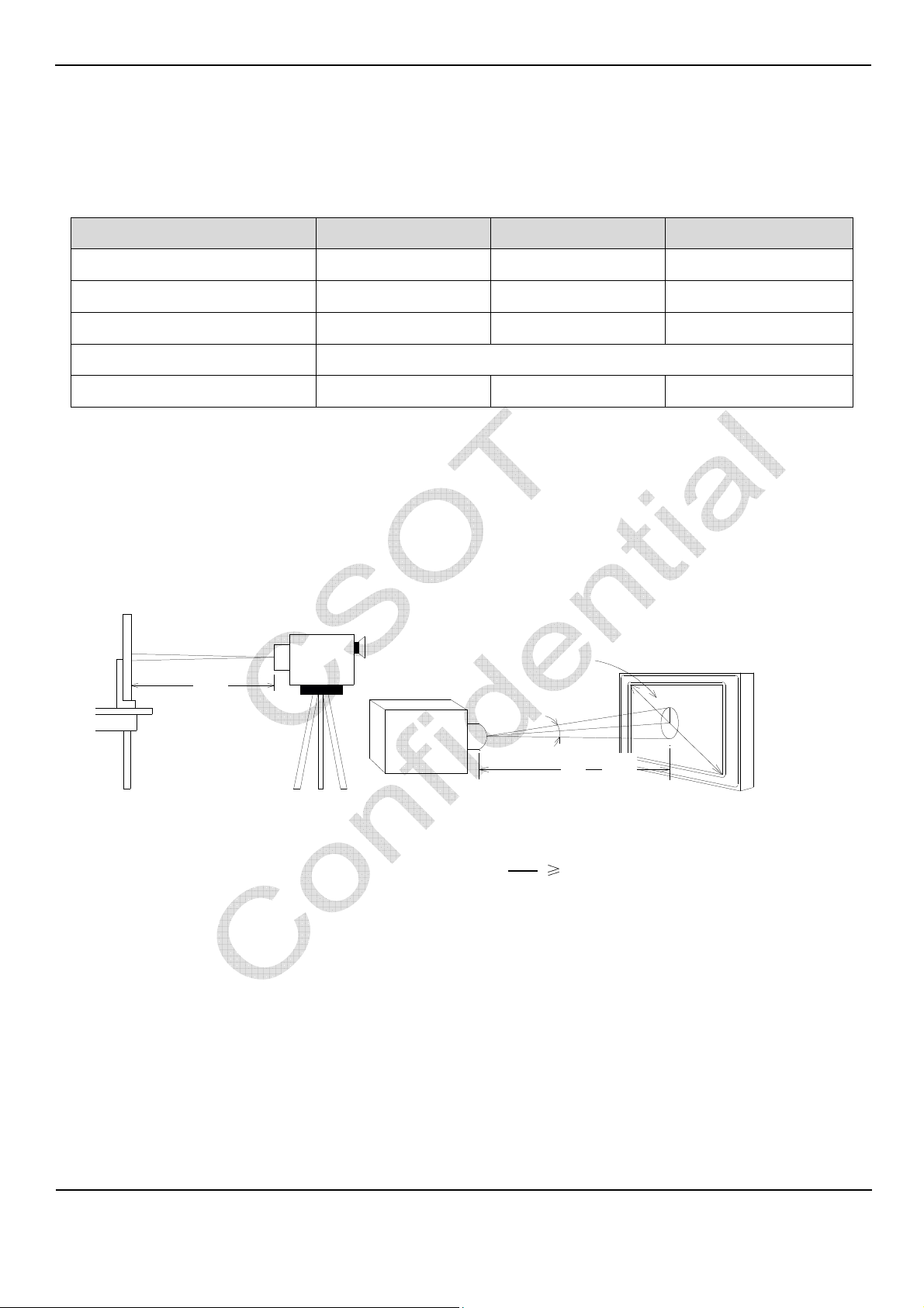
To measure the LCD cell, it is suggested to set up the standard measurement system as Fig. 6.1. The measuring area S
should contain at least 500 pixels ofthe LCD cell as illustrated in Fig.6.2(A means the area allocated to one pixel).In this model,
for example, the minimum measuring distance Z is 370mm when θ is 2 degree. Hence, 500mm is the typical measuring
distance. This measuring condition is referred to 301-2H of VESA FPDM 2.0 about viewing distance, angle, and angular field
of view definition.
θ
Z
For Square
S = πr²
Fig. 6.1The standard set-up system of measurement
θ
r
Z
Fig. 6.2The area S contains at least 500 pixels to be measured
≥
500pixels
N means the actual number of the pixels in the area S.
The copyright belongs to Shenzhen China Star 14 / 22Ver. 0.1
Optoelectronics Technology Co., Ltd.
Any unauthorized use is prohibited.
Page 15
ST4761B01-3 Product Specification
CR-W
6.2 Optical Specifications
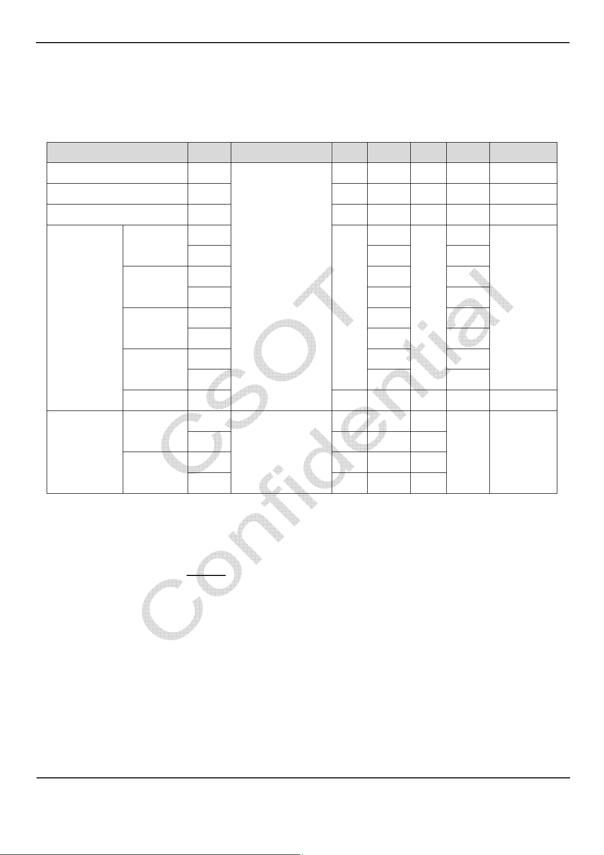
The table below of optical characteristics is measured by MINOLTA CS2000,MINOLTA CA310, ELDIM
OPTIScope-SAand ELDIM EZContrast in dark room.
Item Symbol
Static Contrast Ratio CR
Condition Min.
- 4000 - - (1) (2)
Typ. Max. Unit Note
Response Time TL - 6.5 12 ms (3)
Center Transmittance T% - 5.65 % (2)(4)
Color
Chromaticity
(CIE1931)
Red
Green
Blue
RX
RY
GX
GY
BX
BY
WX
θH=0°, θV=0°
Normal direction at
center point
withCSOT’s module:
MT4761B01-1
Typ.
- 0.03
0.639
0.335
0.319
0.626
0.155
0.052
0.280
Typ.
+0.03
-
-
-
(2) (5)
-
-
-
White
0.290
- 89 -
-
Color Gamut
WY
CG - 72 - % NTSC
θH+
Horizontal
89
89
Deg. (6)
-
Viewing Angle
θH-
θV+
-
CR≥10
-
Vertical
θV-
-
89
-
Note:
(1)Definition of static contrast ratio (CR):
It’s necessary to switch off all the dynamic and dimming function when measuring the static contrast ratio.
Static Contrast Ratio (CR) =
CR-D
CR-W is the luminancemeasured by LMD (light-measuring device) at the center point of the LCD module with full-screen
displaying white. The standard setup of measurement is illustrated in Fig. 6.3; CR-D is the luminance measured by LMD
at the center point of the LCD module with full-screen displaying black. The LMD in this item is CS2000.
(2)The LMD in the item could be a spectroradiometer such as (KONICA MINOLTA) CS2000, CS1000(TOPCON), SR-UL2
or the same level spectroradiometer. Other display color analyzer (KONICA MINOLTA) CA210, CA310 or (TOPCON)
BM-7 could be involved after being calibrated with a spectroradiometer on each stage of a product.
The copyright belongs to Shenzhen China Star 15 / 22Ver. 0.1
Optoelectronics Technology Co., Ltd.
Any unauthorized use is prohibited.
Page 16
100%
0%
X:0%,25%,50%,75%,100%
Black & White
ST4761B01-3 Product Specification
LMD
LCD Module
Fig. 6.3 The standard setup of CR measurement
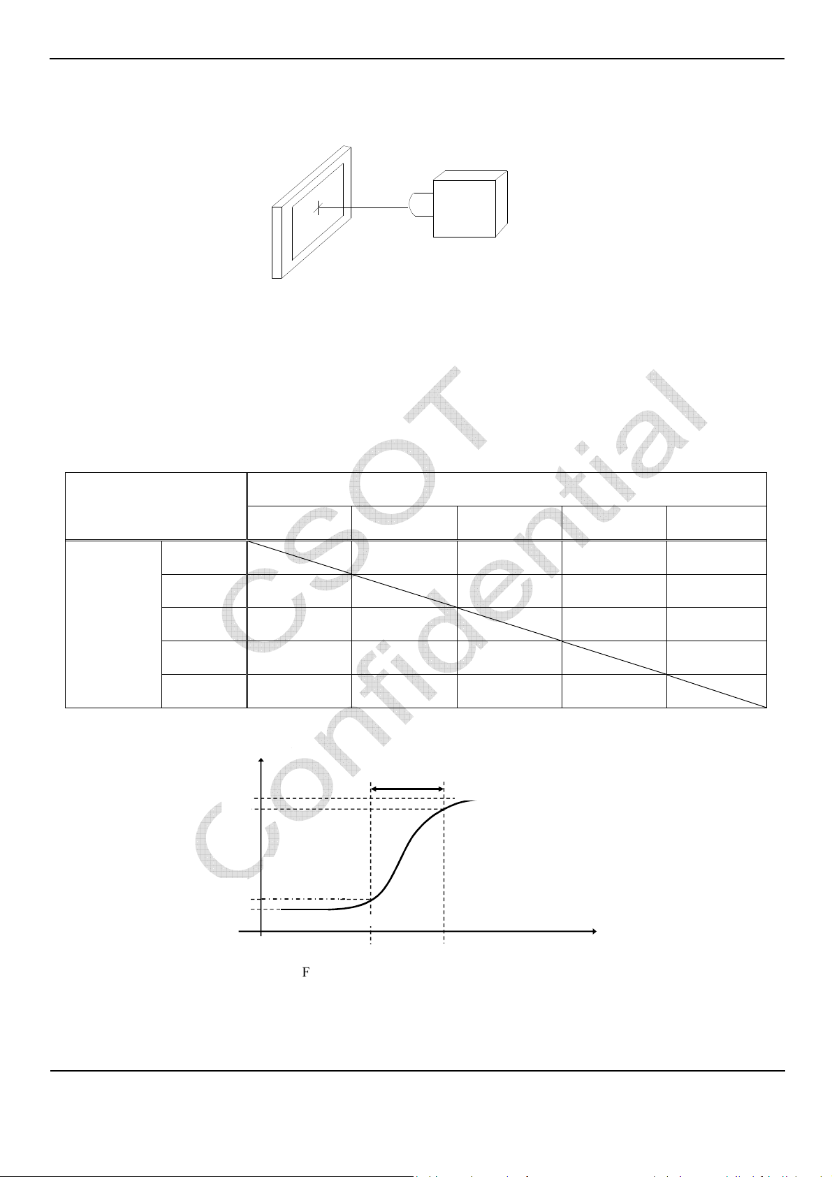
(3) Response time TLis defined as the average transition time in the response time matrix. The table below is the response time
matrix in which each element t
ratiosamong0%,25%,50%,75%, and 100%luminance. The transition time t
90% of the luminance difference between X and Y (X<Y) as illustrated in Fig.6.4. When X>Y, the definition of t
the time taken from 90% to 10% of the luminance difference between X and Y.The response time is optimized on refresh
rate Fr =60Hz.
Measured
Transition Time
0%
Luminance
Ratio of
Current Frame
25% t
50% t
75% t
is the transition time from luminance ratio X to Y. X and Yare two different luminance
X to Y
is defined as the time taken from 10% to
X to Y
Luminance Ratio of Previous Frame
0% 25% 50% 75% 100%
0% to 25%
0% to 50%
0% to 75%
t
t
t
25% to 50%
25% to 75%
25% to 0%
t
t
50% to 0%
t
50% to 25%
50% to 75%
t
t
75% to 0%
75% to 25%
t
75% to 50%
t
t
t
100% to 0%
100% to 25%
100% to 50%
t
100% to 75%
X to Y
is
100% t
t
means the transition time from luminance ratioX to Y.
X to Y
0% to 100%
t
25% to 100%
t
50% to 100%
t
75% to 100%
Luminance
Luminance
t
t
X to Y
100%
90%
90%
X to Y
Y:0%,25%,50%,75%,100%
Y: 0%, 25% 50%, 75%, 100%
Brighter state
Brighter State
Darker State
10%
10%
Darker state
0%
X: 0%, 25% 50%, 75%, 100%
Time
Time
Fig. 6.4The definition of t
X to Y
All the transition time is measured at the center point of the LCD module by ELDIM OPTIScope-SA.
The copyright belongs to Shenzhen China Star 16 / 22Ver. 0.1
Optoelectronics Technology Co., Ltd.
Any unauthorized use is prohibited.
Page 17

(4) Definition of center Transmittance (T%):
Luminance of LCD module
Thetransmittance is measured with full white pattern (Gray 255)
ST4761B01-3 Product Specification
Static Contrast Ratio (CR) =
Luminance of Backlight
(5) Definition of color chromaticity:
Each chromaticity coordinates (x, y) are measured in CIE1931 color space when full-screen displaying primary color R, G,
B and white. The color gamut is defined as the fraction in percent of the area of the triangle bounded by R, G, B
coordinates and the area is defined by NTSC 1953 color standard in the CIE color space. Chromaticity coordinates are
measured by CS2000 and the standard setup of measurement is shown in Fig. 6.5.
Colors
LMD
LCD Module
Fig. 6.5 The standard setup of color chromaticity measurement
(6)Definition of viewing angle coordinate system (θH,θV):
The contrast ratio is measured at the center point of the LCD module. The viewing angles are defined at the angle that the
contrast ratio is larger than 10 at four directions relative to the perpendicular direction of the LCD module(two vertical
angles:up θV+ and downθV-; and two horizontal angles:right θH+ and leftθH-) as illustrated in Fig. 6.6. The contrast ratio is
measured by ELDIM EZContrast.
Y
X
θ
H+
θ
θ
H-
V+
θ
V-
Z
Fig. 6.6Viewing angle coordination system
The copyright belongs to Shenzhen China Star 17 / 22Ver. 0.1
Optoelectronics Technology Co., Ltd.
Any unauthorized use is prohibited.
Page 18
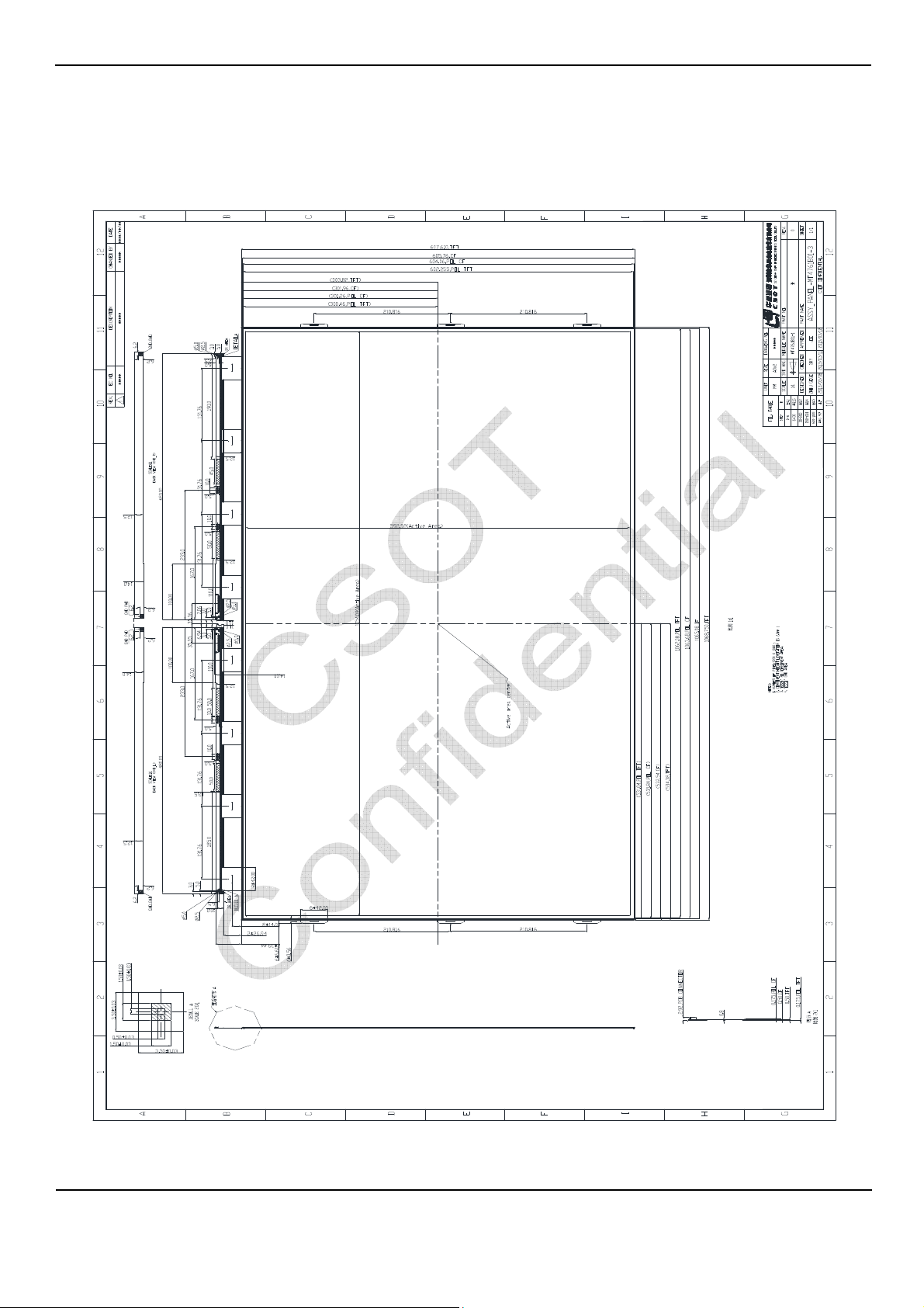
7. MechanicalCharacteristics
7.1Mechanical Specification
ST4761B01-3 Product Specification
The copyright belongs to Shenzhen China Star 18 / 22Ver. 0.1
Optoelectronics Technology Co., Ltd.
Any unauthorized use is prohibited.
Page 19
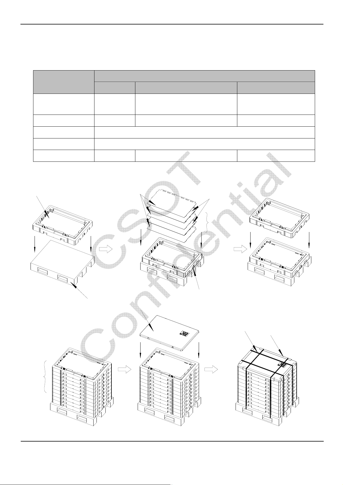
7.2 Packing
7.2.1PackingSpecifications
Item
ST4761B01-3 Product Specification
Specification
Quantity Dimension (mm) Weight (kg)
Packing Box 9 pcs/box 1235(L) x 883 (W) x95 (H)
Net Weight: 18 (Max.)
Gross Weight: 22(Max.)
Pallet 1 1250.00 (L) x 1000.00 (W) x 160.00 (H) Net Weight:22
Stack Layer 10
Boxes per Pallet 10boxes/pallet
Pallet after Packing 90pcs/pallet 1250.0 (L) x 1000.0 (W) x 995.0 (H) Gross Weight:244kg/pallet
7.2.2 PackingMethod
47.6’’EPP Tray
EPE Spacer
Open cell
9pcs Open cell
10pcs EPE Spacer
Pallet
Empty EPP Top Tray
10pcs EPP Tray
The copyright belongs to Shenzhen China Star 19 / 22Ver. 0.1
Optoelectronics Technology Co., Ltd.
Any unauthorized use is prohibited.
2 pcs Carton label on the each side
PP Belt
Corner Protector
Page 20
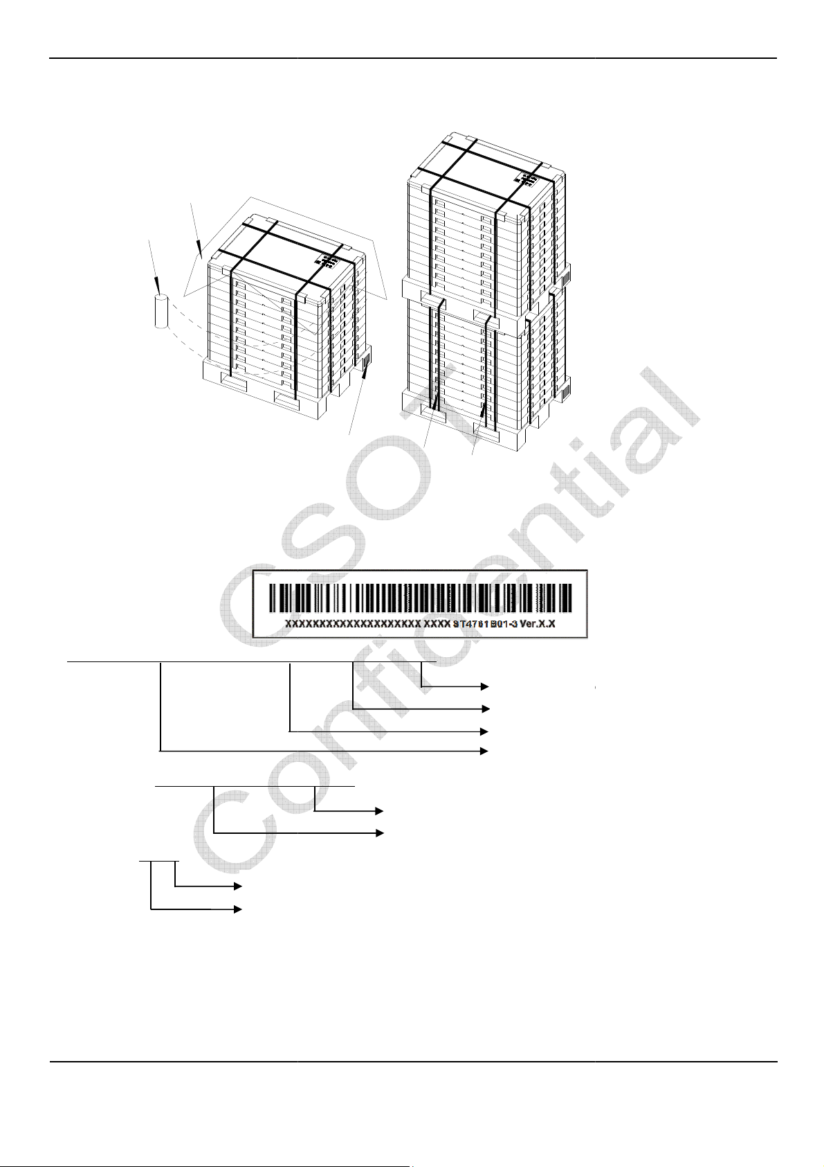
Shenzhen China Star
XXXX
XXXXXXXXXXXXXXXXXXXX
0, 20
Ver.X.X: Version, for example: 0.1, 0.2, … , 1.1, 1.2, …, 2.1, 2.2, …
2 pcs Carton label on the each side
PE Film
Week
Year
ST4761B01
Model Version Code
-3 Product Specification
PE Sheet
8. Definition of Labels
8.1Open CellLabel
XXXXXXXXXXXXXXXXXXXX
Serial Number:
Week Code: XXXX
PP Belt
ST4761B01-3Ver. X.X
CSOT Internal Use
Panel ID
PP Belt
Model Name
Week Code
Serial Number
Year: 2010 =10, 2011 = 11 …2020= 2
Week: 01, 02, 03 …
Model Name: ST4761B01-3
The copyright belongs to
Optoelectronics Technology Co., Ltd.
Any unauthorized use is prohibited.
21= 21…
20 / 22Ver. 0.1
Page 21
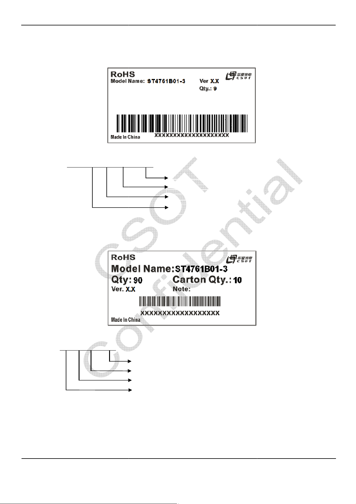
Shenzhen China Star
8.2 Carton Label
XXXXXXXXX
ST4761B01
-3 Product Specification
Serial Number: XXXXXXXX
8.3PalletLabel
Model Name: ST4761B01-3
XXX
CSOT Internal Use
Year, Month, Date
Model Version Code
CSOT Internal Use
Serial Number: XXXXXXXXXXXXX
The copyright belongs to
Optoelectronics Technology Co., Ltd.
Any unauthorized use is prohibited.
CSOT Internal Use
Year, Month
Model Version Code
CSOT Internal Use
21 / 22Ver. 0.1
Page 22

ST4761B01-3 Product Specification
9. Precautions
9.1 Assembly and Handling Precautions
(1) Do not apply rough force such as bending or twisting to the open cell during assembly.
(2) It is recommended to assemble or install a open cell into the user’s system in clean working areas. The dust and
oil may cause electrical shortor damage the polarizer.
(3) Do not apply pressure or impulse to the open cell to prevent the damage to the open cell.
(4) Always follow the correct power-on sequence. This can prevent the damage and latch-up to the LSI chips.
(5) Do not plug in or pull out the interface connector while the open cell is in operation.
(6)Use soft dry clothwithout chemicals for cleaning because the surface of polarizeris very soft and easily be scratched.
(7) Moisture can easily penetrate into the open cell and may cause the damage during operation.
(8) High temperature or humidity may deteriorate the performance of the open cell. Please store open cell in the
specified storageconditions.
(9) When ambient temperature is lower than 10ºC, the display quality might be deteriorated. For example, the
response time will become slow.
9.2 Safety Precautions
(1) If the liquid crystal material leaks from the panel, it should be kept away from the eyes or mouth. In case of
contact with hands, skin or clothes, it has to be washed away thoroughly with soap.
(2)After the open cell end of life, it is not harmful in case of normal operation and storage.
The copyright belongs to Shenzhen China Star 22 / 22Ver. 0.1
Optoelectronics Technology Co., Ltd.
Any unauthorized use is prohibited.
 Loading...