

Page 1
MT5461D01-1 Product Specification
Signature
Date
Approved By Product Director
Date
Reviewed By PM Manager
Date
Reviewed By Project Leader
Date
Reviewed By PM
Date
MODEL: MT5461D01-1
Ver. 1.3
Date:09.Jan.2013
Customer’s Approval
CSOT
Name:
Signature:
Name:
Signature:
Name:
Signature:
Name:
Signature:
The cop yright bel ongs to Shenzhen China Star 1 / 37 Ver.1.3
Opt oe lect ronics Techno log y Co., Ltd.
Any unauthorized us e is prohibited.
Page 2

MT5461D01-1 Product Specification
Contents
Rev ision Histo ry ........................................................................................................................................... 4
1. General Descript ion .................................................................................................................................. 5
1.1 Product Features.............................................................................................................................. 5
1.2 Overview ........................................................................................................................................ 5
1.3 General Informat ion ........................................................................................................................ 5
2. Absolute Maximum Ratings ...................................................................................................................... 6
2.1 Absolute Max imum Ratings (Ta = 25 ± 2 °C) .................................................................................. 6
2.2 Environ ment R equirement............................................................................................................... 6
2.3 Package Storage .............................................................................................................................. 7
3. Electr ical Specification ............................................................................................................................. 8
3.1 Electrical Characteristics ................................................................................................................. 8
3.1.1 Power Consumption (Ta = 25 ± 2 ºC) ................................................................................... 8
3.1.2 V by on e Characteristics ....................................................................................................... 9
3.1.3 V by on e Input Signal Timing ............................................................................................. 10
3.2 Backlight Converter U nit .............................................................................................................. 11
3.2.1 LED Converter Electrical Characteristics (Ta = 25 ± 2 ºC) .................................................. 11
3.2.2 LED Converter Power S equ ence ......................................................................................... 13
4. Input Terminal Pin Assignment ............................................................................................................... 14
4.1 TFT LCD Modu le ......................................................................................................................... 14
4.2 Converter Unit .............................................................................................................................. 16
4.2.1 Co nvert e r Input Connector Pin Definition ........................................................................... 16
4.3 4K2K Data Format ........................................................................................................................ 17
4.4 Color Data Input Assignment ........................................................................................................ 19
5. V-by-One Each Lane Timing Spec .......................................................................................................... 20
5.1 Timing Table (DE Only Mode) ...................................................................................................... 20
5.2 Power On/Off Seque nce ................................................................................................................ 22
5.2.1 Power On/Off Sequence ..................................................................................................... 22
6. Optical Characteristics ............................................................................................................................ 25
6.1 Mea surement C onditions ............................................................................................................... 25
6.2 Optical Sp e cificatio ns ................................................................................................................... 26
7. Mechanical Characteristics ..................................................................................................................... 31
7.1 Mechanical Specification .............................................................................................................. 31
7.2 Packing ......................................................................................................................................... 32
7.2.1 Packing Specifications ........................................................................................................ 33
7.2.2 Packing Method.................................................................................................................. 33
8. D efinition of Labels ................................................................................................................................ 35
The cop yright bel ongs to Shenzhen China Star 2 / 37 Ver.1.3
Opt oe lect ronics Techno log y Co., Ltd.
Any unauthorized us e is prohibited.
Page 3

MT5461D01-1 Product Specification
8.1 Module Label ................................................................................................................................ 35
8.2 Carton Label ................................................................................................................................. 35
8.3 Pallet Label ................................................................................................................................... 36
9. Precautions ............................................................................................................................................. 37
9.1 Assemb ly and Handling Precautions .............................................................................................. 37
9.2 Safety Precautions ......................................................................................................................... 37
The cop yright bel ongs to Shenzhen China Star 3 / 37 Ver.1.3
Opt oe lect ronics Technology Co., Ltd.
Any unauthorized use is prohibi ted.
Page 4
MT5461D01-1 Product Specification
Revision History
Version Date Page (New) Section Description Revision by
Ver. 0.1 15.Oct.2012 37 All
Ver. 1.1 1.Dec.2012 37 All
Ver. 1.2 12.Dec.2012 26 6.2
Ver. 1.3 9.Jan.2013 31 7.1
Tentative Specification was First Issued.
Chenguo W u
Preliminar y Specification was First Issued Chenguo W u
Modify Center Luminance. Chenguo W u
Update Mechanical Specification. Chenguo W u
The cop yright bel ongs to Shenzhen China Star 4 / 37 Ver.1.3
Opt oe lect ronics Technology Co., Ltd.
Any unauthorized use is prohibi ted.
Page 5
1. General Description
1.1 Product Features
- QFHD Resolution (3840 x 2160)—2D
- 4K1K Resolution (38 40 x 1080)—3D
- High Brightnes s: 400 cd/m²—2D,50 cd/m²—3D
- Very High Contrast Ratio: 4000:1
- Fast Response Time
- High Color Satu ra t i o n: 72% NTSC
- Ultra Wide Viewing Angle: 178° (H)/178° (V) (CR ≥ 10)
- Low Power Cons umption: Typ. 135 W
- DE (Data Enable) Mode
- V by One Interface
1.2 Overview
MT5461D01-1 Product Specification
MT5461D01-1 is a diagonal 54.6”color active matrix LCD module with edge LED backlight and 8 lanes V by one
interface. This module is a transmissive type display operating in th e normally bla ck m ode. It supports 3840 x 2160 QFHD
resolution and can disp l ay up t o 1073.7M colors (10bit). Each pixel is divided into Red, Green and Blue sub-pixels which ar e
arranged in vertical stripe. The converter of backlight is built-in.
This module dedica tes for LC D T V products and provides excell ent per formance which in cludes high brightness, ultra
wide viewing angle, high color sa turation and high color depth.
1.3 General Information
Item Specification Unit Note
Active Area 1209.6 (H) x 680.4 (V) mm
Bezel Opening Area 1215.8 (H) x 686.6 (V) mm
Outline Dimension 1225.8 (H) x 696.6 (V) x 15.1 (D) mm D: From Be zel t o Re ar
Weight 16 kg Max.
Driving Scheme a-Si TFT Active Matrix -
Number of Pixels 3840 x 2160 pixel
Pixel Pitch (Sub Pixel) 0.105 (H) x 0.315 (V) mm
Pixel Arrangeme nt RGB Vertical Stripe -
Display Colors 1073.7M color 10bit
Display Mode Transmissive Mode, Normally Black -
Surface Treatment Anti-glare, Haze 2%, Hard Coati ng (3H) -
Luminance of White
The cop yright bel ongs to Shenzhen China Star 5 / 37 Ver.1.3
Optoelect ronics T ec hno log y Co., Ltd.
Any unauthorized use is prohibi ted.
400—2D,50—3D
cd/m² Center Point, Typ.
Page 6

MT5461D01-1 Product Specification
2. Absolute Maximum Ratings
2.1 Absolute Maxim um R ati ng s (Ta = 25 ± 2 °C)
The followings a re maximum values whic h, if exceeded, may cau se d amage to the unit.
Value
Item Symbol
Min. Max.
Power Supply Voltage VCC -0.3 14.0 V
Input Signal Voltage VIN -0.3 4.0 V
V
58 69
W(2D)
Light Bar Voltage
V
71 77
W(3D)
Converter Input Voltage VBL 0 30 V
Con t rol Signal Le ve l - -0.3 7.0 V
Unit
V
RMS
2.2 Environment Requirement
(1) Temperature and relative humidity range are shown as below.
Relative Humidity (%RH)
100
90
80
60
Operating Range
40
-40
(a) 90%RH maximum (Ta ≤ 39 ºC).
(b) Wet-bu lb temperature should be 39 ºC maximum (Ta > 39 ºC).
20
Storage Ra nge
10
0
20
Fig. 2.1 Operating and storage environment
39 ºC, 90%
40
60 -20
Tem perature (ºC)
80
(c) No condensati on.
(2) The storage tempera ture is between - 20 ºC to 60 ºC, and the operatin g ambient temperature is between 0 ºC to 50 ºC.
The max imu m oper a tin g tem per atur e i s based on th e test condi tion that th e sur fa ce tem per at ur e of disp la y ar ea is les s th an
or equal to 65 ºC with LC D module in a temperature controlled chamber alone. Thermal management should be considered
in fin al produ ct de sign t o pre vent the s urfa ce temper ature of display ar ea fr om being over 65 ºC. The range of oper ating
temper ature may degr ade in case of im proper therm al managemen t in the e nd product design.
(3) The TFT module includ ing glass should be avoided any shock or vibration.
The cop yright bel ongs to Shenzhen China Star 6 / 37 Ver.1.3
Optoelect ronics T ec hno log y Co., Ltd.
Any unauthorized use is prohibi ted.
Page 7

MT5461D01-1 Product Specification
While t est ing sh ock an d vi br a t ion , the fixture holding the module shoul d be a s sur e d to be ha rd an d r igi d en ou gh to pr e ven t
the module twisted or bent by the fixture. The test conditions should be less th an:
Shock (Non-operating): 35 G, 11 ms, half sine wave, 1 time for ± X, ± Y, ± Z.
Vibration (Non-operating): Random 1.0 Grms, 10 ~ 200 Hz, 10 min, 1 time for each X, Y, Z.
2.3 Package Storage
When storing modules as spares for a long time, please follow the precaution instructions:
(1) Do n ot store the module in high temperature and high humidity for a long time. It is highly recommended to store the
module with temperature from 0 ºC to 35 ºC in normal humidity.
(2) The module shall be stored in a dark area and avoided to be ex posed in direct sunlight or fluorescent light.
The cop yright bel ongs to Shenzhen China Star 7 / 37 Ver.1.3
Optoelect ronics T ec hno log y Co., Ltd.
Any unauthorized use is prohibi ted.
Page 8
MT5461D01-1 Product Specification
B
B
B
B
R
G
R
R
R
G
G
G
B
R
R
R
R
G
G
G
G
B
B
B
3. Electrical Specification
3.1 Electrical Characteristics
3.1.1 Power Consumption (Ta = 25 ± 2 ºC)
Value
Parameter Symbol
Min. Typ. Max.
Power Supply Voltage VCC 10.8 12.0 13.2 V (1)
Unit Note
Rush Current I
White P attern Icc - - 1.1 A
Power Supply
Horizontal Stripe Icc - - 3 A
Current
Black Pattern Icc - - 1.1 A
Note:
(1) The ripple voltage should be control led less than 10% of V
(2) Measurement condition: V
(3) Measurement condition: V
A. White Patt e r n B. Hor izontal Pattern
rising ti me = 470 μs.
CC
VCC x 0.1
GND
Fig. 3.1 VCC rising time condition
= 12 V, Ta = 25 ± 2 ºC, F = 120 Hz. The test patter ns are shown as below.
CC
RUSH
470 μs
- - 4 A (2)
(3)
.
CC
VCC
V
x 0.9
CC
C. Black Pat tern
Fig. 3.2 Test patterns
The cop yright bel ongs to Shenzhen China Star 8 / 37 Ver.1.3
Optoelect ronics T ec hno log y Co., Ltd.
Any unauthorized use is prohibi ted.
Page 9
3.1.2 V by One Characteristics
Differential Input High
Differential Input Low
Parameter
Threshold Voltage
Threshold Voltage
V by one Interface
Common Input Voltag e
Differential Input Voltage |VID| - - - mV
Terminating Re s istor RT 90 100 110 ohm
MT5461D01-1 Product Specification
Value
Symbol
Min. Typ. Max.
V
- - +50 mV
TH
V
- 50 - - mV
TL
V
- - - V
CM
Unit
Input High Threshold Voltage V
2.4 - 3.3 V
IH
CMOS Interface
Input Low Threshold Voltage VIL - - 0.6 V
The cop yright bel ongs to Shenzhen China Star 9 / 37 Ver.1.3
Optoelect ronics T ec hno log y Co., Ltd.
Any unauthorized use is prohibi ted.
Page 10
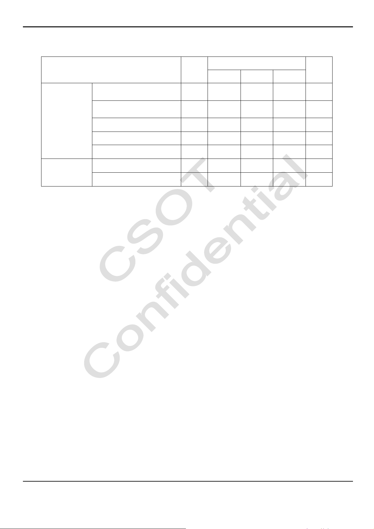
3.1.3 V by One Input Signal Timi ng
F
E
tREYE
mV
Parameter Symbol Condition Min. Typ. Max. Unit
MT5461D01-1 Product Specification
3-byte 380 tTCIP/30 1667 PS
Unit Interval (VBO Operation Bit Rate)
Eye Width At Package Pin
Eye Width Positio n A at Package Pin
Eye Width Position B at Package Pin tB - - 0.3 - UI
Eye Width Position C at Package Pin tC - - 0.7 - UI
Eye Width Position D at Package Pin tD - - 0.75 - UI
Eye Width Position E at Package Pin tE - - 0.7 - UI
Eye Width positio n F at Package Pin tF - - 0.3 - UI
Intra-pair Skew TTOSK_intra - -0.3 - 0.3 UI
Inter-pair Skew TTOSK_inter - -500 - 500 UI
tRBIT
tREYE - - 0.5 - UI
tA - - 0.25 - UI
4-byte 285 tTCIP /40 1250 PS
5-byte 266 tTCIP /50 1000 PS
tRBIT
B C
A
D
Y- 0
X=0 UI
Fig. 3.3 V by one input signal tim ing
The cop yright bel ongs to Shenzhen China Star 10 / 37 Ver. 1.3
Optoelect ronics T ec hno log y Co., Ltd.
Any unauthorized use is prohibi ted.
Page 11

3.2 Backlight Converter Unit
3.2.1 LED Converter Electrical Characteristics (Ta = 25 ± 2 ºC)
MT5461D01-1 Product Specification
Parameter Symbol
Unit Note
Min. Typ. Max.
Value
- 124.6 143.3 W
P
BL(2D)
No dim ming
att
Power Consumpti on
P
- 76 84.2 W
BL(3D)
att
Input Voltage VBL 22.8 24.0 25.2 V
I
BL(2D)
- 5.19 6.63
A No dimming
Input Current
I
BL(3D)
I
- - 5
RS-VIN
- 3.17 3.69
A
A (1)
Input Inrush Current
I
On/Off Control Voltage
On
- - 12
RS-EN
2.5 3.3 3.6 V
V
BLON
A (2)
Off 0.0 - 0.8 V
On/Off Control Current
PWM Dimming Control Voltage
- I
Max.
- - 1.5 mA
BLON
V
V
PDIM
2.5 3.3 3.6
Min. 0.0 - 0.8 V
External PWM Control Current
I
- - 2 mA
P-DIM
PWM Dimming Frequency F
Dimming Duty Ratio D
150 160 170 Hz
PWM
10
DIM
-
DET HI Open Collector
DET Status Signal
DET Low 0
Input Impedance RIN 300
Note:
(1) Th e measurement condition: V
BL
(2) The measurement condition: the V
rising ti me is 20 ms. (V
= 24V, and then on the V
BL
from 10% ~ 90%)
BL
= 3.3V.
BLON
(3) Less t han 10% dimming c ontrol is functional well and no backlight happens to shut down.
100 % (3)
0.8 V
Kohm
The cop yright bel ongs to Shenzhen China Star 11 / 37 Ver.1.3
Optoelect ronics T ec hno log y Co., Ltd.
Any unauthorized use is prohibi ted.
Page 12
MT5461D01-1 Product Specification
VBL
20ms
V
BLON
t
I
RS-VIN
I
RS-EN
IBL
t
t
Fig. 3.4 The timing sequen ce diagram of inrush current measurement
The cop yright bel ongs to Shenzhen China Star 12 / 37 Ver. 1.3
Optoelect ronics T ec hno log y Co., Ltd.
Any unauthorized use is prohibi ted.
Page 13

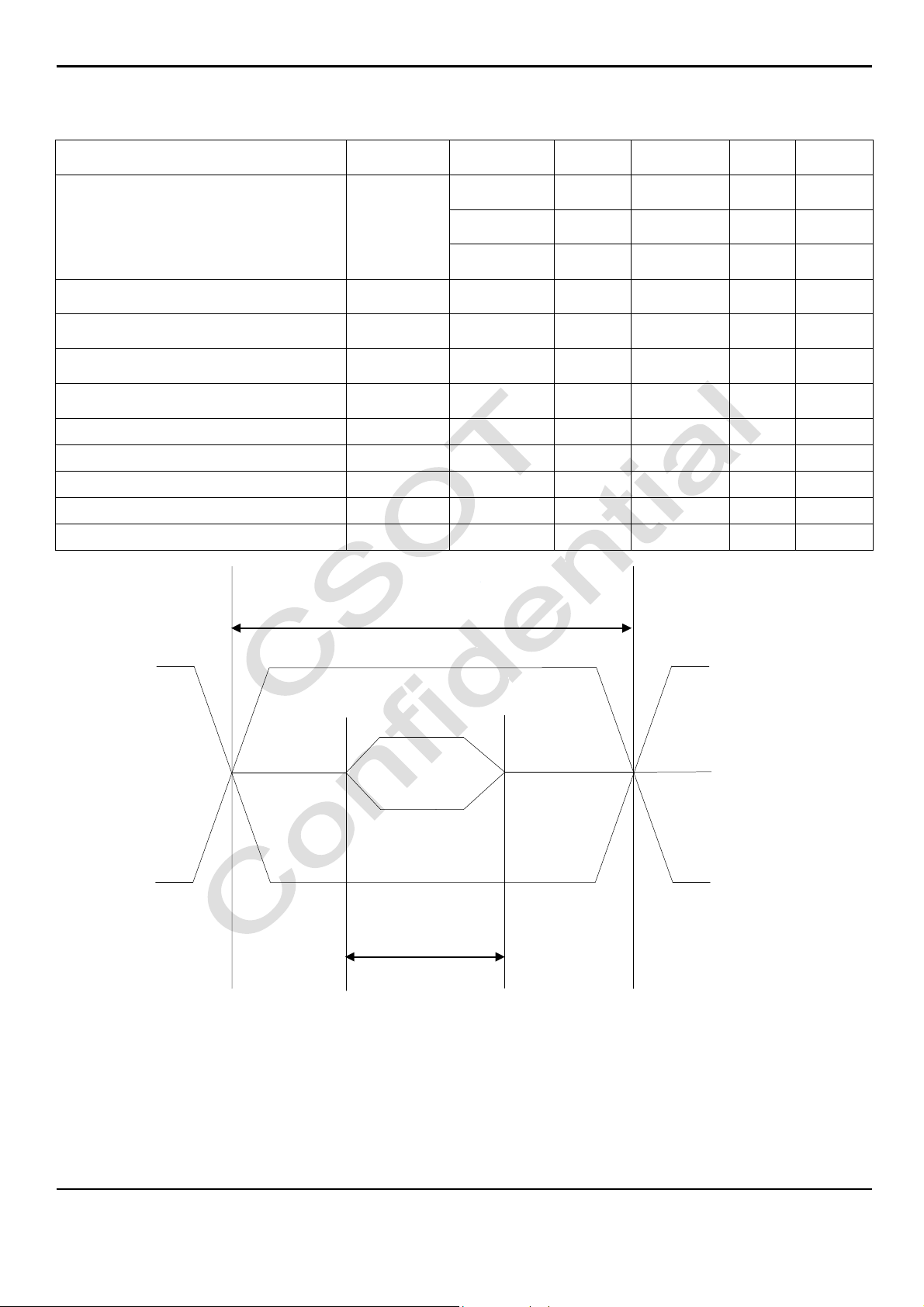
3.2.2 LED Converter Power Sequence
Tr1
0.1VBL
0.9 VBL
MT5461D01-1 Product Specification
No ITEM SYMBOL MIN. TYP. MAX. UNIT
1 VBL Rising T ime Tr 20 - - ms
2 VBL Falling Time Tf 20 - - ms
3 VBLON Rising Time Tr1 - - 100 ms
4 VBLON Falling Time Tf1 - - 100 ms
VBL to VP_DIM Delay
5
T1 500 - - ms
Time
6 BLON Delay Time T2 250 - - ms
7 BLON Off Time T3 0 - - ms
8 VP_DIM Off Time T4 250 - - ms
V
BL
0
0.9VBL
0.1V
BL
T1
Tr
REMARK
See Fig.3.5
T4
Tf
V
P_DIM
V
BLON
Note: The power sequence
V
:
POWER ON
POWER OFF
BL > VP_DIM >VBLON
V
V
:
BLON >= VP_DIM> VBL
Any other single( sync, 3D_EN,2D/3D)>VBL
T2
Tf1
Fig. 3.5 The power sequence of V
:
any other single( sync, 3D_EN,2D/3D)
BL >
2.0V
0.8V
T3
2.0V
0.8V
and V
BL
BLON
The cop yright bel ongs to Shenzhen China Star 13 / 37 Ver. 1.3
Optoelect ronics T ec hno log y Co., Ltd.
Any unauthorized use is prohibi ted.
Page 14

4. Input Terminal Pin Assignment
4.1 TFT LCD Mo d ule
CN1: CT000041-513C (P-TWO)
Pin No. Symbol Description Note
1 VIN12 Power 12V in (1)
2 VIN12 Power 12V in (1)
3 VIN12 Power 12V in (1)
4 VIN12 Power 12V in (1)
5 VIN12 Power 12V in (1)
6 VIN12 Power 12V in (1)
7 VIN12 Power 12V in (1)
8 NC (1)
9 GND Ground (1)
MT5461D01-1 Product Specification
10 GND Ground (1)
11 Rx0N Vx1 Lane0- (1)
12 Rx0P Vx1 Lane0+ (1)
13 GND Ground (1)
14 Rx1N Vx1 Lane1- (1)
15 Rx1P Vx1 Lane1+ (1)
16 GND Ground (1)
17 Rx2N Vx1 Lane2- (1)
18 Rx2P Vx1 Lane2+ (1)
19 GND Ground (1)
20 Rx3N Vx1 Lane3- (1)
21 Rx3P Vx1 Lane3+ (1)
22 GND Ground (1)
23 HTPDN Hot Plug Detect (1)
24 LOCKN Lock Detect (1)
25 GND Ground (1)
26 Rx4N Vx1 Lane4- (1)
27 Rx4P Vx1 Lane4+ (1)
28 GND Ground (1)
29 Rx5N Vx1 Lane5- (1)
30 Rx5P Vx1 Lane5+ (1)
31 GND Ground (1)
32 Rx6N Vx1 Lane6- (1)
33 Rx6P Vx1 Lane6+ (1)
The cop yright bel ongs to Shenzhen China Star 14 / 37 Ver. 1.3
Optoelect ronics T ec hno log y Co., Ltd.
Any unauthorized use is prohibi ted.
Page 15

MT5461D01-1 Product Specification
CN1
34 GND Ground (1)
35 Rx7N Vx1 Lane7- (1)
36 Rx7P Vx1 Lane7+ (1)
37 GND Ground (1)
38 3D_SYNC_I Shutter Glass Sync Input Signal (1)
39 3D_SYNC_O Shutter Glass Sync Signal (1)
40 3D_EN 3D_EN Signal (1)
41 NC (2)
42 NC (2)
43 NC (2)
44 NC (2)
45 NC (2)
46 NC (2)
47 NC (2)
48 NC (2)
49 NC (2)
50 NC (2)
51 NC (2)
Note:
(1)The direction of pi n assignmen t is shown as below:
#1
#51
Fig. 4.1 Connector direction sketch map
(2) For CSOT internal only, pl ease let it open.
Attention: Default JEDIA mode
(1)
(2)
The cop yright bel ongs to Shenzhen China Star 15 / 37 Ver. 1.3
Optoelect ronics T ec hno log y Co., Ltd.
Any unauthorized use is prohibi ted.
Page 16

4.2 Converter Unit
4.2.1 Converter Inp ut Connector Pin Definiti on
CN1: CT000019-143N(FCN) (see 4.2 Note (1))
MT5461D01-1 Product Specification
Pin No. Symbol Feature
1
2
V
3
Power Sup ply, + 24 V DC Regulated
BL
4
5
6
7
8
GND GND
9
10
11
12
13
DET Normal (0 ~ 0.8 V), Abnormal (Open Collector)
BLON BLON/OFF
NC NC
Note
(1)
Note (1):
14
P_DIM PWM Dimming Control
#1
#1
Fig. 4.2 Power input connector direction sketch map
#14
CN1
CN1
#14
The cop yright bel ongs to Shenzhen China Star 16 / 37 Ver. 1.3
Optoelect ronics T ec hno log y Co., Ltd.
Any unauthorized use is prohibi ted.
Page 17

4.3 4K2K Data Format
Lane4-Lane7
2D Mode:
MT5461D01-1 Product Specification
Scan Out1
Scan Out2 2
Scan Out3 3
Scan Out4 4
………………
Scan Out2160
2160
1
Pixel1
…………. ……………
Pixel2
Pixel1919
Pixel1920
Pixel1921
Pixel1922
1920
Lane0-Lane3
Left Right
1920
Pixel3839
Pixel3840
TCON
Vx1
Fig. 4.3 2D data format
3840*2160 60Hz in
TCON
Vx1
The cop yright bel ongs to Shenzhen China Star 17 / 37 Ver. 1.3
Optoelect ronics T ec hno log y Co., Ltd.
Any unauthorized use is prohibi ted.
Page 18

3D Mode:
MT5461D01-1 Product Specification
Scan Out1
Scan Out2 1
Scan Out3 2
Scan Out4 2
………………
Scan Out2160
1080
1
Pixel1
…………. ……………
Pixel2
Pixel1919
Pixel1920
Pixel1921
Pixel1922
1920
Lane0-Lane3
Left Right
1920
Pixel3839
Lane4-Lane7
Pixel3840
TCON
Vx1
Fig. 4.4 3D data format
3840*1080 120Hz in
TCON
Vx1
The cop yright bel ongs to Shenzhen China Star 18 / 37 Ver. 1.3
Optoelect ronics T ec hno log y Co., Ltd.
Any unauthorized use is prohibi ted.
Page 19

4.4 Color Data Input Assignment
B9
The br ightn ess of ea ch prim ary color is base d on th e 10-bit gray scal e data input for each color. The higher th e binary
input, the bright e r the col or. Th e t able bel ow provides t he assignm ent of the c olor versus.
Data Signal
MT5461D01-1 Product Specification
Data Input Color
Basic Colors
Gray Scale of Red
Red Green Blue
MSB LSB
R9 R8 R7 R6 R5 R4 R3 R2 R1 R0 G9 G8 G7 G6 G5 G4 G3 G2 G1 G0
Black 0 0 0 0 0 0 0 0 0 0 0 0 0 0 0 0 0 0 0 0 0 0 0 0 0 0 0 0 0 0
Red (1023) 1 1 1 1 1 1 1 1 1 1 0 0 0 0 0 0 0 0 0 0 0 0 0 0 0 0 0 0 0 0
Green (1023) 0 0 0 0 0 0 0 0 0 0 1 1 1 1 1 1 1 1 1 1 0 0 0 0 0 0 0 0 0 0
Blue (1023) 0 0 0 0 0 0 0 0 0 0 0 0 0 0 0 0 0 0 0 0 1 1 1 1 1 1 1 1 1 1
Cyan 0 0 0 0 0 0 0 0 0 0 1 1 1 1 1 1 1 1 1 1 1 1 1 1 1 1 1 1 1 1
Magenta 1 1 1 1 1 1 1 1 1 1 0 0 0 0 0 0 0 0 0 0 1 1 1 1 1 1 1 1 1 1
Yellow 1 1 1 1 1 1 1 1 1 1 1 1 1 1 1 1 1 1 1 1 0 0 0 0 0 0 0 0 0 0
White 1 1 1 1 1 1 1 1 1 1 1 1 1 1 1 1 1 1 1 1 1 1 1 1 1 1 1 1 1 1
Red (000) 0 0 0 0 0 0 0 0 0 0 0 0 0 0 0 0 0 0 0 0 0 0 0 0 0 0 0 0 0 0
Red (001) 0 0 0 0 0 0 0 0 0 1 0 0 0 0 0 0 0 0 0 0 0 0 0 0 0 0 0 0 0 0
:
: : : : : : : : : : : : : : : : : : : : : : : : : : : : : : : : : : : : : : : : : : : : : : : : : : : : : : : : : : :
:
Red (1022) 1 1 1 1 1 1 1 1 1 0 0 0 0 0 0 0 0 0 0 0 0 0 0 0 0 0 0 0 0 0
MSB LSB
MSB LSB
B8 B7 B6 B5 B4 B3 B2 B1 B0
:
Red (1023) 1 1 1 1 1 1 1 1 1 1 0 0 0 0 0 0 0 0 0 0 0 0 0 0 0 0 0 0 0 0
Green (000) 0 0 0 0 0 0 0 0 0 0 0 0 0 0 0 0 0 0 0 0 0 0 0 0 0 0 0 0 0 0
Green (001) 0 0 0 0 0 0 0 0 0 0 0 0 0 0 0 0 0 0 0 1
:
Gray Scale of Green
Green (1022) 0 0 0 0 0 0 0 0 0 0 1 1 1 1 1 1 1 1 1 0 0 0 0 0 0 0 0 0 0 0
Green (1023) 0 0 0 0 0 0 0 0 0 0 1 1 1 1 1 1 1 1 1 1 0 0 0 0 0 0 0 0 0 0
Blue (000) 0 0 0 0 0 0 0 0 0 0 0 0 0 0 0 0 0 0 0 0 0 0 0 0 0 0 0 0 0 0
Blue (001) 0 0 0 0 0 0 0 0 0 0 0 0 0 0 0 0 0 0 0 0 0 0 0 0 0 0 0 0 0 1
Gray Scale of Blue
Blue (1022) 0 0 0 0 0 0 0 0 0 0 0 0 0 0 0 0 0 0 0 0 1 1 1 1 1 1 1 1 1 0
Blue (1023) 0 0 0 0 0 0 0 0 0 0 0 0 0 0 0 0 0 0 0 0 1 1 1 1 1 1 1 1 1 1
: : : : : : : : : : : : : : : : : : : : : : : : : : : : : : : : : : : : : : : : : : : : : : : : : : : : : : : : : : :
:
:
: : : : : : : : : : : : : : : : : : : : : : : : : : : : : : : : : : : : : : : : : : :
:
Attention:
0: Low level voltage; 1: High level voltage.
0 0 0 0 0 0 0 0 0 0
: : : : : : : : : : : : : : :
:
:
:
The cop yright bel ongs to Shenzhen China Star 19 / 37 Ver. 1.3
Optoelect ronics T ec hno log y Co., Ltd.
Any unauthorized use is prohibi ted.
Page 20

5. V-by-One Each Lane Timing Spec
5.1 Timing Table (DE O nly Mode)
2D Mode:
Signal Item Symbol Min. Typ. Max. Unit Note
F
Frequency
Fram e Ra te F - 60 - Hz
CLK
(= 1 / T
CLK
MT5461D01-1 Product Specification
- 74.25 - MHz (1)
)
Vertical
Term
Total TV - 2250 - TH TV = TVD + TVB
Display TVD 2160
T
H
Blank TVB - 90 - TH
Total T
- 550 - T
H
TH = THD + THB
CLK
Horizontal
Display THD 480
T
CLK
Term
Blank THB - 70 - T
CLK
3D Mode:
Signal Item Symbol Min. Typ. Max. Unit Note
Frequency
CLK
(= 1 / T
CLK
)
- 74.25 - MHz (1)
F
Fram e Ra te F - 120 - Hz
Vertical
Term
Total TV - 1125 - TH TV = TVD + TVB
Display TVD 1080 T
H
Blank TVB - 45 - TH
Total T
Horizontal
Display THD 480
- 550 - T
H
TH = THD + THB
CLK
T
CLK
Term
Blank THB - 70 - T
CLK
Attention:
The module is operated in DE only mode, H sync and V sync inpu t s ignal have no effect on normal operation.
Note:
(1) Please make sur e the range of pixel clock follo ws th e followin g equations:
Fclkin(max) ≥ Fr6 × Tv× Th
Fr5 × Tv × Th ≥ Fclkin(min)
The cop yright bel ongs to Shenzhen China Star 20 / 37 Ver. 1.3
Optoelect ronics T ec hno log y Co., Ltd.
Any unauthorized use is prohibi ted.
TV
Page 21

MT5461D01-1 Product Specification
THB
TVD TVB
DE
TH
DCLK
DE
T
CLK
THD
DATA
Valid Display Data (960CLK)
Fig. 5.1 Interface signal timing diagram
The cop yright bel ongs to Shenzhen China Star 21 / 37 Ver. 1.3
Optoelect ronics T ec hno log y Co., Ltd.
Any unauthorized use is prohibi ted.
Page 22

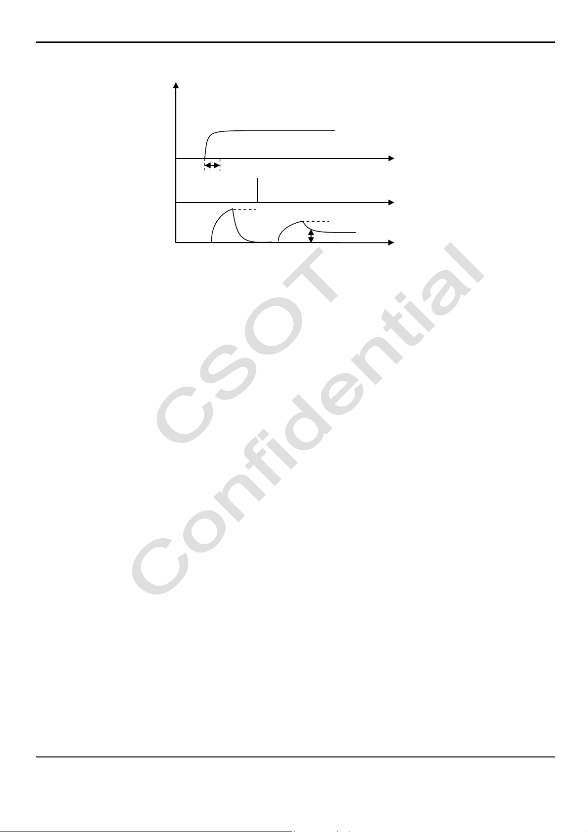
5.2 Po wer On/Off Sequence
50%
0.9 VCC
0.9 VCC
5.2.1 Power On/Off Sequen ce
To preven t a latch-up or DC opera tion of LCD module, th e power on/off sequence should be as th e diagram below.
V
CC
0 V
MT5461D01-1 Product Specification
0.1 V
CC
Vx1 Signals
Option Signals
(2D/3D L/R)
V
BLON
0 V
T1
T2
Valid Data
Power On
T7 T8
50%
T5
Fig. 5.2 Power on/off sequence
T3
T4
Power Off
T6
The cop yright bel ongs to Shenzhen China Star 22 / 37 Ver. 1.3
Optoelect ronics T ec hno log y Co., Ltd.
Any unauthorized use is prohibi ted.
Page 23

MT5461D01-1 Product Specification
0.1 VCC
0.9 VCC
50%
5.2.2 2D/3D C hange Signal Sequence wit hout Vcc Turn off and Turn on
V
CC
0 V
Vx1 Signals
2D/3D
V
BLON
0 V
Parameter
T1
T2
Power On
T7
T5
Fig. 5.3 2D/3D power on/off sequence
Values
Min. Typ. Max.
T9
Unit
T1 0.5 - 10.0 ms
T2 0.0 - - ms
T3 0.0 - - ms
T4 1000 - - ms
T5 500 - - ms
T6 100 - - ms
T7 - - T2 ms
T8 - - T3 ms
T9 0.0 - 10.0 ms
Attention:
(1)While system turn from 2D/3D function to 3D/2D function,the V
(2) The supply voltage of the external system for the module input should follow the definition of V
The cop yright bel ongs to Shenzhen China Star 23 / 37 Ver. 1.3
Optoelect ronics T ec hno log y Co., Ltd.
Any unauthorized use is prohibi ted.
signal should be always high .
BLON
CC
.
Page 24

MT5461D01-1 Product Specification
(3) Apply the lightbar voltage within the LCD operation range. When the ba ckl igh t tur ns on befor e th e LC D oper ati on or th e
LCD turns off befor e the backlight turns off, the displa y m ay momentari ly become abnormal sc reen.
(4) In case that V
is in off l evel, pl ease keep th e level of in put signa ls on the low or high impedan ce. If T2 < 0, th at ma y
CC
cause el ect rical over s tress.
(5) T4 shou ld be mea sured after the module has been fully discharged between power off and on period.
(6) Interface signal shall not be kept at high impedance when the p ower is on.
The cop yright bel ongs to Shenzhen China Star 24 / 37 Ver. 1.3
Optoelect ronics T ec hno log y Co., Ltd.
Any unauthorized use is prohibi ted.
Page 25

6. Optical Characteristics
S
A
6.1 Measurement Conditions
The table below is the test condition of optical measurement.
Item Symbol Val ue Unit
MT5461D01-1 Product Specification
Ambie nt Tempera ture TA
Ambient Humidity HA
25±2
50±10
ºC
% RH
Supply Voltage VCC 63 V
Driving S ignal Refer to the typical value in Chapter 3: Electrical Specification
Light Source Curr ent (Each Unit) IL 110 mA
Ver t ical Refresh Rate FR 60 Hz
To avoid abrupt temperature change during optical measurement, it’s suggested to warm up the LCD module more than 60
minutes after lighting the backlight and in the windless environment.
To measure th e LC D m odule, it is suggested to set up the s tandard mea surement system as Fig. 7.1. The measuring area S
should contain at least 500 pixe ls of the LCD module as illustrated in Fig. 7.2 (A means the area allocated to one pixel). In this
model, for exam p le, the minim um measuring distance Z is 370 mm when θ is 2 degree. Hence, 500 mm is t he typical
mea s urin g distance. This me as uring condition is referred to 301-2H of VESA FPDM 2.0 about viewing distance, angle, and
angular field of view definition.
θ
S = πr²
Z
For Square
θ
r
Z
Fig. 6.1 The standard set-up system of measurement
The cop yright bel ongs to Shenzhen China Star 25 / 37 Ver. 1.3
Optoelect ronics T ec hno log y Co., Ltd.
Any unauthorized use is prohibi ted.
Fig. 6.2 The area S contains at least 500 pixels to be measured
N =
≥ 500 pixels
N mean s th e actual number of t he pixels in the area S.
Page 26

MT5461D01-1 Product Specification
CR-W
6.2 Optical Specif icat i ons
The table below of optical characteristics is measured by MINOLTA CS2000, MINOLTA CA310, ELDIM OPTI
Scope-SA and ELDIM EZ Contrast in dark room.
Item Symbol Condition Min. Typ. Max. Unit Note
Static Contrast Ratio CR
- 4000 - - (1) (2)
(3) OPTI
Response Time TL - 6.5 - ms
Scope-SA
L
400 - cd/m2 (2) (4)
W-2D
Center Luminance
L
- 50 - - (5)
W -3D
3D Crosstalk CT-3D - 3.5% - - (5)
Unifor mity of White Screen - 70 75 - % (2) (6)
R
X
Red
RY
G
X
= 0°, θV = 0°
θ
H
Normal direction at
center p oint of the
LCD module.
0.642
0.337
0.327
-
-
-
Green
Color
Chromaticity
(CIE1931)
Blue
GY
BX
Typ.
- 0.03
BY
W
0.280 -
X
0.626
0.157
0.055
Typ.
+ 0.03
(2) (7)
-
-
White
WY 0.290 -
Color Gamut CG - 72 - % NTSC (2) (7)
θ
H+
- 89 -
Horizontal
89
89
-
(8)
Deg.
-
V iew ing A ngle
θ
H-
-
CR ≥ 10
θ
V+
-
Vertical
θ
V-
-
89
-
Note:
(1) Definition of static contrast ratio (CR):
It’s necessary to switch off all the dynamic and dimming function when measuring the stati c contrast ratio.
Static Contrast Ratio (CR) =
CR-D
CR-W is the luminance measured by LMD (light-measuring device) at the center point of the LCD module with
full-screen displ aying white. T he standard setup of measurement is illustrated in Fig. 6.3; CR-D is the luminance measured
by L M D at the cent er p oint of the LCD module with full-screen displaying black.
(2) The LMD in the item could be a spectroradiometer such as (KONICA MINOLTA) CS2000, CS1000, (TOPCON)
The cop yright bel ongs to Shenzhen China Star 26 / 37 Ver. 1.3
Optoelect ronics T ec hno log y Co., Ltd.
Any unauthorized use is prohibi ted.
Page 27

MT5461D01-1 Product Specification
X: 0%, 25%, 50%, 75%, 100%
100%
10%
SR-UL2 or the same level spectroradiometer. Other display col or analyzer (KONICA MINOLTA) CA210, CA310 or
(TOPCON) BM-7 could be involved after being cal ibrated with a sp ectroradi om eter on each st ag e of a product.
Black & White
LMD
LCD Module
Fig. 6.3 The standard setup of CR measurement
(3) Response time T
time matrix in which each element t
luminance ratios among 0%, 25%, 50%, 75%, and 100% luminance. The transition time t
from 10 % t o 9 0% of the luminance difference between X and Y ( X < Y) as illustrated in Fig6.4. When X > Y, the
definition of t
optimized on refresh rate F
Measured
is defined as the average transition time in the response time matrix. The table below is the response
L
is the transition time from luminance ratio X to Y. X and Y are two different
X to Y
is defined as the time taken
X to Y
is the time taken from 9 0 % t o 10% of the luminan ce di ff erence between X and Y. The response time is
X to Y
= 60Hz.
R
Luminance Rati o of Previous Frame
Luminance
Ratio of
Current Frame
t
means the transition tim e from luminance ratio X to Y.
X to Y
Transition Time
25% t
50% t
75% t
100% t
90%
0%
0% 25% 50% 75% 100%
0% t
0% to 25%
t
0% to 50%
t
0% to 75%
0% to 100%
Luminance
t
t
X to Y
Darker S tate
25% to 0%
25% to 50%
25% to 75%
25% to 10 0%
t
t
t
t
50% to 25%
50% to 75%
50% to 100%
50% to 0%
t
t
t
Y: 0%, 25%, 50%, 75%, 100%
Darker S tate
75% to 0%
75% to 25%
t
75% to 50%
75% to 100%
t
t
t
100% to 0%
100% to 25%
100% to 50%
t
100% to 75%
The cop yright bel ongs to Shenzhen China Star 27 / 37 Ver. 1.3
Optoelect ronics T ec hno log y Co., Ltd.
Any unauthorized use is prohibi ted.
Fig. 6.4 The definition of t
X to Y
Time
Page 28

MT5461D01-1 Product Specification
All the transition time is measured at the center point of the LCD module by ELDIM OPTI Scope-SA.
(4) Definition of center luminance (L
The lum in ance is measured at the center poin t of the LCD module with full-screen displa ying white. Fig. 6.5 shows t he
standard setup of l u minance meas urement.
(5) Definition of the 3D mode performance:
Test pattern
Pattern Left eye image Right eye image remark
WW
):
W
White
LMD
LCD Module
Fig. 6.5 The standard setup of lu minance measurement
Left eye image: L2 5 5
Right eye image:L255
L(WW) is d enoted as the l uminance of “WW”
WB
BW
BB
LCD Module
Fig. 6.6 3D optical measurement system
3D optical
Shutter glasses
Left eye image: L2 5 5
Right eye image:L0
L(WB) is denoted as the luminance of “WB”
Left eye image: L0
Right eye image:L255
L(BW) is denoted as the luminance of “BW”
Left eye image: L0
Right eye image:L0
L(BB) is denoted as th e luminance of “BB”
Measur e th e center poin t of the LCD module through the shutter glasses unde r 3D mode ope ration.
The cop yright bel ongs to Shenzhen China Star 28 / 37 Ver. 1.3
Optoelect ronics T ec hno log y Co., Ltd.
Any unauthorized use is prohibi ted.
Page 29

MT5461D01-1 Product Specification
(1)
(4)
(3)
(2)
(5)
(6)
(7)
(8)
(9)
V/9
V/9
V/2
V/2
V
L(WB)-L(BB)
The 3D lum in ance (Lw-3D) is the luminan ce measured by LMD with well controlled shutter glasses a t the center point of the
LCD module wi th tes t pattern L(WW).
The 3D crosstalk is measuremd at the center point of the LCD module through right-eye glasses..
Definition of the 3D mode crosstalk:
CT-3D =
L(BW)-L(BB)
(6) Definition of uniformity of white screen:
The lum in ance Li (i fr om 1 to 9) is meas ured at the 9 points defined in Fig. 6.7. H and V indicate active area.
From th e measured s et of lumin ance valu es Li (i from 1 to 9), the minimum luminance is den oted as L
luminance is denoted as L
Unifor mity = L
min
/ L
max
.The uniformity of white screen is defined accordin g to
max.
x 100%.
H
H/9
H/2
H/2
H/9
(7) Definition of color chromaticity:
Fig. 6.7 Symbol “ + ” defines the 9 measuring locations (1), (2), (3) ··· (9)
and th e ma ximum
min
Each chr omaticity coordinates (x, y) are m easur ed in CIE1931 color spa ce when ful l-screen displaying primary color R, G, B
and white. The color g amu t is defi n ed as th e fra cti on in p ercen t of th e ar ea of th e tri an gl e boun ded b y R, G, B coordi n at es a n d
the ar ea is defined by NTSC 1953 color standard in the CIE color space. Chromati city coor dinates are measur ed by CS2000
and the standard setup of measurement is shown in Fig. 6.8.
Colors
LMD
LCD Module
Fig. 6.8 The standard setup of color chromaticity measurement
(8) Definition of viewing angle coordinate system (θH, θV):
The con tr ast rati o i s m easured at the center poin t of the LCD module. The viewing angles are defined at the angle that the
contrast ratio is larger than 10 at four directions relative to the perp en dicular direction of the LCD module (two vertica l angles:
The cop yright bel ongs to Shenzhen China Star 29 / 37 Ver. 1.3
Optoelect ronics T ec hno log y Co., Ltd.
Any unauthorized use is prohibi ted.
Page 30

MT5461D01-1 Product Specification
up θV+ and down θV-; and two horizontal angles: right θH+ and left θH-) as illustrated in Fig. 6.9. The contrast ratio is measured
by ELDIM EZ Contrast.
Y
X
θ
H+
θ
θ
H-
θ
V+
V-
Z
Fig. 6.9 Viewing angle coordination system
The cop yright bel ongs to Shenzhen China Star 30 / 37 Ver. 1.3
Optoelect ronics T ec hno log y Co., Ltd.
Any unauthorized use is prohibi ted.
Page 31

7. Mechanical Characteristics
7.1 Mechanical Specification
MT5461D01-1 Product Specification
The cop yright bel ongs to Shenzhen China Star 31 / 37 Ver. 1.3
Optoelect ronics T ec hno log y Co., Ltd.
Any unauthorized use is prohibi ted.
Page 32

MT5461D01-1 Product Specification
The cop yright bel ongs to Shenzhen China Star 32 / 37 Ver. 1.3
Optoelect ronics T ec hno log y Co., Ltd.
Any unauthorized use is prohibi ted.
Page 33

7.2 Packing
Masking Tape
LCD TV Module
Panel Protector
7.2.1 Packing Specifications
Item
Quantity Dimension (mm) Weight (kg)
MT5461D01-1 Product Specification
Specification
Packing Box 5 pcs / box 1357.0 (L) x 365.0 (W) x 798.0 (H)
Net Weig h t: 80.0
Gross Weight:88.7
Pallet 1 1420 (L) x 1120 (W) x 150 (H) Net Weight:32
Stack La yer 1
Boxes per Pallet 3 boxes / pallet
Pall et after Packin g 15 pcs / pallet 1420 (L) x 1120 (W) x951(H) Gross Weight: 299
7.2.2 Packing Method
PE Bag
Carton
Bottom Cushion
LCD TV Module(5pcs)
Eart h Box
Top Cushion
Box Tape
PP Belt
Carton Label(2pcs)
Fig. 7.1 Packing method (protector film stick on the front of the LCD module)
The cop yright bel ongs to Shenzhen China Star 33 / 37 Ver. 1.3
Optoelect ronics T ec hno log y Co., Ltd.
Any unauthorized use is prohibi ted.
Page 34

MT5461D01-1 Product Specification
PE Film(2Layers)
Corner Protector(1)
Corner Protector(3)
Corner Protector(2)
PE Sheet
PP Belt
Pallet
Pallet Label(2sides)
Exceed 1 0 0 mm to the pallet
Pallet(Plastic:1420*1120*150mm)as
Out of the PE F ilm
Fig. 7.2 Shipping method
The cop yright bel ongs to Shenzhen China Star 34 / 37 Ver. 1.3
Optoelect ronics T ec hno log y Co., Ltd.
Any unauthorized use is prohibi ted.
Page 35

MT5461D01-1 Product Specification
Week
Year
CSOT Internal Use
Panel ID
8. Definition of Labels
8.1 Module Label
For RoHs compatible products, CSOT will add RoHS for identification.
Model Name: MT5461D01-1
Ver.X.X: Version, for example: 0.1, 0.2, … , 1.1, 1.2, …, 2.1, 2.2, …
WC (Week Code): XX XX
Year: 2010 = 10, 2011 = 11 … 2020 = 20, 2021 = 21…
Week: 01, 02, 03 …
Serial Number: XXXXXXXXXXXX XXXXXXXX
8.2 Carton Label
Model Name: MT5461D01-1
The copyright belongs to Shenzhen China Star 35 / 37 Ver.1.3
Optoelectronics Technology Co., Ltd.
Any unauthorized use is prohibited.
Page 36

Serial Number: XXXXX XX XXXXX XXXXX
CSOT Internal Use
Model Version Code
Year, Month, Date
CSOT Internal Use
CSOT Internal Use
Model Version Code
Year, Month
CSOT Internal Use
Manufactured Date:
Year: 2010 = 10, 2011 = 11…2020 = 20, 2021 = 21…
Month: 1~9, A~C, for Jan. ~ Dec.
Date: 01~31, for 1st to 31st
Model Version Code: Version of product, for example: 01, 02, 11, 12…
8.3 Pallet Label
MT5461D01-1 Product Specification
Model Name: MT5461D01-1
Serial Number: XXX XX XXX XXXXX
The copyright belongs to Shenzhen China Star 36 / 37 Ver.1.3
Optoelectronics Technology Co., Ltd.
Any unauthorized use is prohibited.
Page 37

MT5461D01-1 Product Specification
9. Precautions
9.1 Assembly and Handling Precautions
(1) Do not apply rough force such as bending or twisting to the LCD module during assembly.
(2) It is recommended to assemble or install a LCD module into the user’s system in clean working areas. The dust
and oil may cause electrical short or damage the polarizer.
(3) Do not apply pressure or impulse to the LCD module to prevent the damage to LCD panel and backlight.
(4) Always follow the correct power-on sequence. This can prevent the damage and latch-up to the LSI chips.
(5) Do not plug in or pull out the interface connector while the module is in operation.
(6) Do not disassemble the LCD module.
(7) Use soft dry cloth without chemicals for cleaning because the surface of polarizer is very soft and easily be
scratched.
(8) Moisture can easily penetrate into the LCD module and may cause the damage during operation.
(9) High temperature or humidity may deteriorate the performance of the LCD module. Please store LCD modules in
the specified storage conditions.
(10) When ambient temperature is lower than 10ºC, the display quality might be deteriorated. For example, the
response time will become slow, and the starting voltage of LED light bar will be higher than that in room
temperature.
9.2 Safety Precautions
(1) If the liquid crystal material leaks from the panel, it should be kept away from the eyes or mouth. In case of
contact with hands, skin or clothes, it has to be washed away thoroughly with soap.
(2) After the LCD module’s end of life, it is not harmful in case of normal operation and storage.
The copyright belongs to Shenzhen China Star 37 / 37 Ver.1.3
Optoelectronics Technology Co., Ltd.
Any unauthorized use is prohibited.
 Loading...