

Page 1
MT3151A05-1 Product Specification
Customer’s Approval
CSOT
Signature
Date
Approved By Product Director
Name: Richard Lung
Signature:
Date
Reviewed By PM Manager
Name: Aaron Tu
Signature:
Date
Reviewed By Project Leader
Name: Richard Lung
Signature:
Date
Reviewed By PM
Name: Teng Ma
Signature:
Date
MODEL: MT3151A05-1
Ver. 2.1
Date: 8.Jun.2012
The copyright belongs to Shenzhen China Star 1 / 30 Ver. 2.1
Optoelectronics Technology Co., Ltd.
Any unauthorized use is prohibited.
Page 2
MT3151A05-1 Product Specification
Contents
Revision History ................................................................................................................................................ 4
1. General Description ....................................................................................................................................... 5
1.1 Product Features .................................................................................................................................. 5
1.2 Overview .............................................................................................................................................. 5
1.3 General Information ............................................................................................................................. 5
2. Absolute Maximum Ratings .......................................................................................................................... 6
2.1 Absolute Maximum Ratings ................................................................................................................ 6
2.2 Environment Requirement ................................................................................................................... 6
2.3 Package Storage.......................................................................................................................... ......... 7
3. Electrical Specification .................................................................................................................................. 8
3.1 Electrical Characteristics ..................................................................................................................... 8
3.1.1 Power Consumption .................................................................................................................. 8
3.1.2 LVDS Characteristics ................................................................................................................ 9
3.2 Backlight Converter Unit ................................................................................................................... 10
3.2.1 LED Converter Electrical Characteristics............................................................................... 10
3.2.2 LED Converter Power Sequence ............................................................................................ 11
4. Electrical Block Diagram............................................................................................................................. 12
5. Input Terminal Pin Assignment ................................................................................................................... 13
5.1 TFT LCD Module .............................................................................................................................. 13
5.2 Converter Unit ................................................................................................................................... 15
5.2.1 Converter Input Connector Pin Definition.............................................................................. 15
5.3 Block Diagram of Interface ............................................................................................................... 16
5.4 LVDS Interface .................................................................................................................................. 16
5.4.1 VESA Format (SELLVDS = L or Open) ................................................................................ 16
5.4.2 JEIDA Format (SELLVDS = H) ............................................................................................. 16
5.5 Color Data Input Assignment ............................................................................................................ 17
6. Interface Timing ........................................................................................................................................... 18
6.1 Timing Table (DE Only Mode) .......................................................................................................... 18
6.2 Power On/Off Sequence .................................................................................................................... 19
7. Optical Characteristics ................................................................................................................................. 20
7.1 Measurement Conditions ................................................................................................................... 20
7.2 Optical Specifications ........................................................................................................................ 21
8. Mechanical Characteristics .......................................................................................................................... 25
8.1 Mechanical Specification ................................................................................................................... 25
8.2 Packing............................................................................................................................................... 27
8.2.1 Packing Specifications ............................................................................................................ 27
The copyright belongs to Shenzhen China Star 2 / 30 Ver. 2.1
Optoelectronics Technology Co., Ltd.
Any unauthorized use is prohibited.
Page 3

MT3151A05-1 Product Specification
9. Definition of Labels ..................................................................................................................................... 28
9.1 Module Label ..................................................................................................................................... 28
9.2 Carton Label ...................................................................................................................................... 28
9.3 Pallet Label ........................................................................................................................................ 28
10. Precautions ................................................................................................................................................. 30
10.1 Assembly and Handling Precautions ............................................................................................... 30
The copyright belongs to Shenzhen China Star 3 / 30 Ver. 2.1
Optoelectronics Technology Co., Ltd.
Any unauthorized use is prohibited.
Page 4
MT3151A05-1 Product Specification
Version
Date
Page (New)
Section
Description
Revision by
Ver. 0.1
6.Jan.2012
30
10
Preliminary Specification was First Issued.
Teng Ma
Ver. 1.1
8.Mar.2012
30
10
Tentative Specification.
Teng Ma
Ver. 2.1
8.Jun.2012
30
10
Approval Specification.
Teng Ma
8
3.1.1
Update Vertical Pattern.
Teng Ma
18
6.1
Update Timing Table.
Teng Ma
21
7.2
Update Optical Specifications.
Teng Ma
23
7.2
Update (5) Definition of uniformity of white screen.
Teng Ma
27
8.2.2
Update packing specification.
Teng Ma
27
8.2.1
Update packing method.
Teng Ma
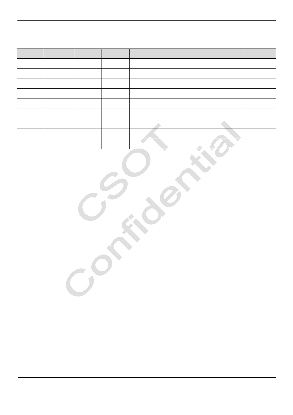
Revision History
The copyright belongs to Shenzhen China Star 4 / 30 Ver. 2.1
Optoelectronics Technology Co., Ltd.
Any unauthorized use is prohibited.
Page 5
1. General Description
Item
Specification
Unit
Note
Active Area
697.685 (H) x 392.256 (V)
mm
Bezel Opening Area
705.4 (H) x 400.0 (V)
mm
Outline Dimension
735.4 (H) x 433.0 (V) x 10.8 (D)
mm
D: From Bezel to Rear (Thinner)
Weight
4.5
kg
Max.
Driving Scheme
a-Si TFT Active Matrix
-
Number of Pixels
1366 x 768
pixel
Pixel Pitch (Sub Pixel)
0.51075 (H) x 0.17025 (V)
mm
Pixel Arrangement
RGB Horizontal Stripe
-
Display Colors
16.7 M
color
8-bit
Display Mode
Transmissive Mode, Normally Black
-
Surface Treatment
Anti-glare, Haze 2%, Hard Coating (3H)
-
Luminance of White
300
cd/m²
Center Point, Typ.
1.1 Product Features
- HD Resolution (1366 x 768)
- Brightness: 300 cd/m²
- Very High Contrast Ratio: 3000:1
- Fast Response Time
- Color Saturation: 62% NTSC
- Ultra Wide Viewing Angle: 178° (H)/178° (V) (CR 10)
- Low Power Consumption: Typ. 36 W
- DE (Data Enable) Mode
- LVDS (Low Voltage Differential Signaling) Interface
- ROHS Compliance
1.2 Overview
MT3151A05-1 Product Specification
MT3151A05-1 is a diagonal 31.5” color active matrix LCD module with edge LED backlight and 1ch-LVDS interface.
This module is a transmissive type display operating in the normally black mode. It supports 1366 x 768 HD resolution and
can display up to 16.7M colors (8-bit). Each pixel is divided into Red, Green and Blue sub-pixels which are arranged in
horizontal stripe. The converter of backlight is built-in.
This module dedicates for LCD TV products and provides excellent performance which includes high contrast ratio, ultra
wide viewing angle, low power consumption and high color depth.
1.3 General Information
The copyright belongs to Shenzhen China Star 5 / 30 Ver. 2.1
Optoelectronics Technology Co., Ltd.
Any unauthorized use is prohibited.
Page 6
2. Absolute Maximum Ratings
Item
Symbol
Value
Unit
Min.
Max.
Power Supply Voltage
VCC
- 0.3
13.5
V
Input Signal Voltage
VIN
- 0.3
3.6
V
Converter Input Voltage
VBL 0 30
V
Control Signal Level
-
- 0.3
7.0
V
80
60
-20
40 0 20
-40
100
90
80
40
60
20
10
Relative Humidity (%RH)
Temperature (ºC)
Operating Range
Storage Range
39 ºC , 90%
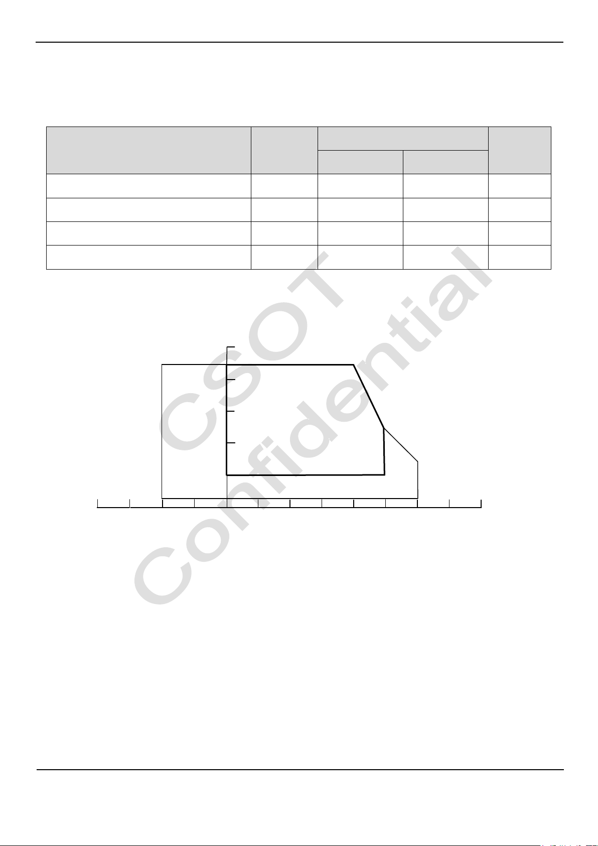
2.1 Absolute Maximum Ratings (TA = 25 ± 2 °C)
The followings are maximum values which, if exceeded, may cause damage to the unit.
2.2 Environment Requirement
(1) Temperature and relative humidity range are shown as below.
MT3151A05-1 Product Specification
(a) 90%RH maximum (TA < 39 ºC).
(b) Wet-bulb temperature should be 39 ºC maximum (TA > 39 ºC).
(c) No condensation.
(2) The storage temperature is between - 20 ºC to 60 ºC , and the operating ambient temperature is between 0 ºC to 50 ºC .
The maximum operating temperature is based on the test condition that the surface temperature of display area is less than
or equal to 65 ºC with LCD module in a temperature controlled chamber alone. Thermal management should be considered
in final product design to prevent the surface temperature of display area from being over 65 ºC. The range of operating
temperature may degrade in case of improper thermal management in the end product design.
(3) The TFT module including glass should be avoided any shock or vibration.
While testing shock and vibration, the fixture holding the module should be assured to be hard and rigid enough to prevent
the module twisted or bent by the fixture. The test conditions should be less than:
The copyright belongs to Shenzhen China Star 6 / 30 Ver. 2.1
Optoelectronics Technology Co., Ltd.
Any unauthorized use is prohibited.
Page 7

MT3151A05-1 Product Specification
Shock (Non-operating): 35 G, 11 ms, half sine wave, 1 time for ± X, ± Y, ± Z.
Vibration (Non-operating): Random 1.0 Grms, 10 ~ 200 Hz, 10 min, 1 time for each X, Y, Z.
2.3 Package Storage
When storing modules as spares for a long time, please follow the precaution instructions:
(1) Do not store the module in high temperature and high humidity for a long time. It is highly recommended to store the
module with temperature from 0 ºC to 35 ºC in normal humidity.
(2) The module shall be stored in a dark area and avoided to be exposed in direct sunlight or fluorescent light.
The copyright belongs to Shenzhen China Star 7 / 30 Ver. 2.1
Optoelectronics Technology Co., Ltd.
Any unauthorized use is prohibited.
Page 8
3. Electrical Specification
Parameter
Symbol
Value
Unit
Note
Min.
Typ.
Max.
Power Supply Voltage
VCC
10.8
12.0
13.2 V (1)
Rush Current
I
RUSH
- - 3 A
(2)
Power Supply
Current
White Pattern
ICC - 0.2
0.3
A
(3)
Vertical Stripe
ICC - 0.4
0.5
A
Black Pattern
ICC - 0.2
0.3
A
GND
VCC
VCC x 0.1
VCC x 0.9
470 μs
3.1 Electrical Characteristics
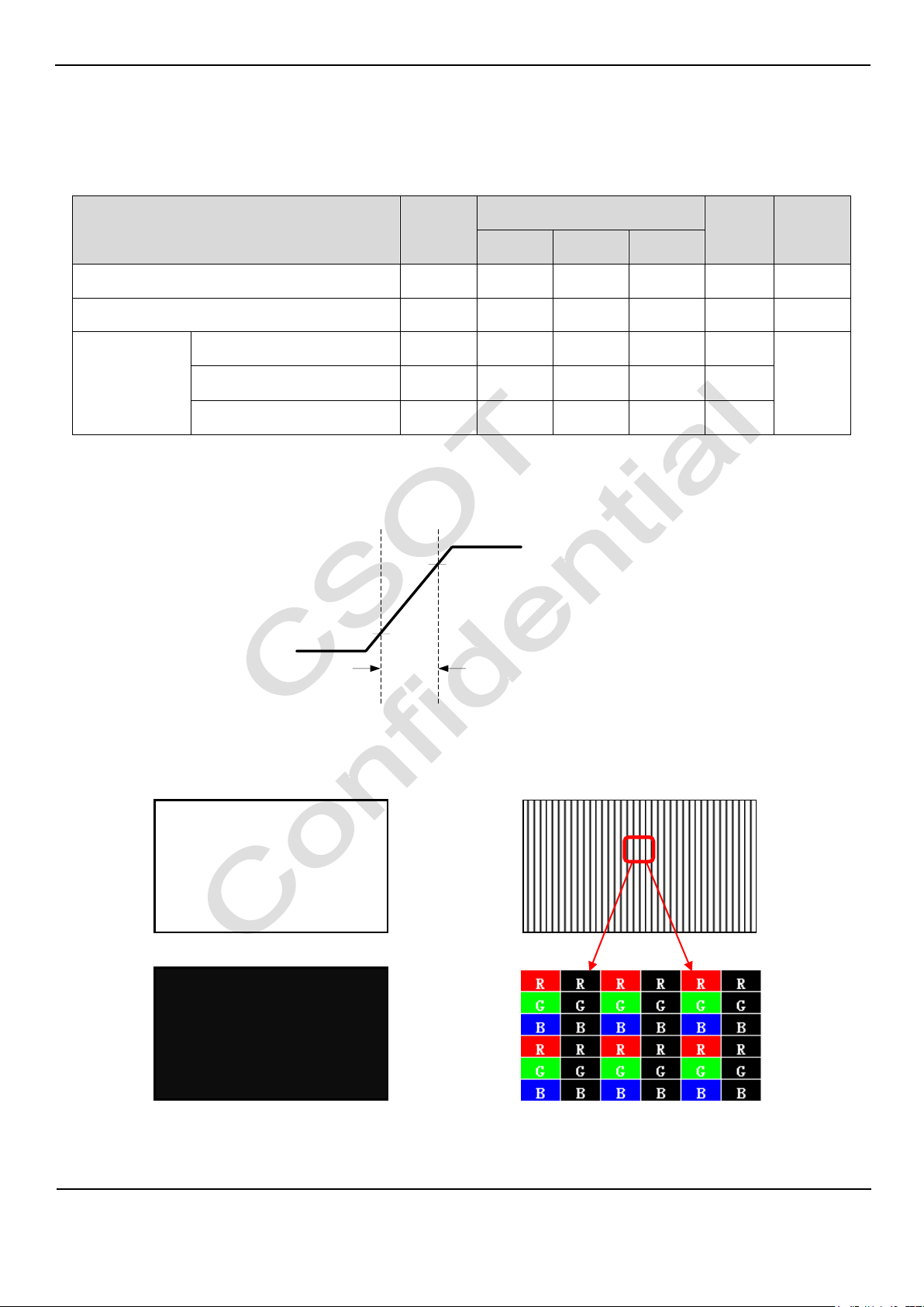
3.1.1 Power Consumption (TA = 25 ± 2 ºC )
Note:
(1) The ripple voltage should be controlled less than 10% of VCC.
MT3151A05-1 Product Specification
(2) Measurement condition: VCC rising time = 470 μs.
Fig. 3.1 VCC rising time condition
(3) Measurement condition: VCC = 12 V, TA = 25 ± 2 ºC, F = 60 Hz. The test patterns are shown as below.
A. White Pattern B. Vertical Pattern
C. Black Pattern
Fig. 3.2 Test patterns
The copyright belongs to Shenzhen China Star 8 / 30 Ver. 2.1
Optoelectronics Technology Co., Ltd.
Any unauthorized use is prohibited.
Page 9
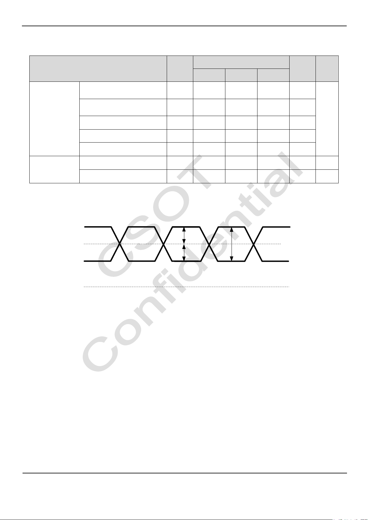
3.1.2 LVDS Characteristics
Parameter
Symbol
Value
Unit
Note
Min.
Typ.
Max.
LVDS Interface
Differential Input High
Threshold Voltage
VTH
+ 100 - -
mV
(1)
Differential Input Low
Threshold Voltage
VTL - -
- 100
mV
Common Input Voltage
VCM
1.0
1.2
1.4
V
Differential Input Voltage
|VID|
200 - 600
mV
Terminating Resistor
RT - 100
-
ohm
CMOS Interface
Input High Threshold Voltage
VIH
2.7 - 3.3 V
Input Low Threshold Voltage
VIL
0.0 - 0.6 V
VTH
VTL
|VID|
VCM
GND
Note:
MT3151A05-1 Product Specification
(1) The LVDS input signal has been defined as follows:
Fig. 3.3 LVDS input signal
The copyright belongs to Shenzhen China Star 9 / 30 Ver. 2.1
Optoelectronics Technology Co., Ltd.
Any unauthorized use is prohibited.
Page 10

3.2 Backlight Converter Unit
Parameter
Symbol
Condition
Value
Unit
Note
Min.
Typ.
Max.
Power Consumption
PBL
VBL = 24V
-
25 - W
(1)
Input Voltage
VBL
-
22.8
24.0
25.2 V
Input Current
IBL
V
BL
= 24V
-
1.04
1.3
A
(1)
Input Inrush Current
I
RS-VIN
VBL = 24V
- - 2.7
A
(2)
- - 5
A
On/Off Control
Voltage
On
V
BLON
V
BL
= 24V
2.5 - 5.0 V
Off
V
BL
= 24V
0.0 - 0.8 V
On/Off Control
-
I
BLON
V
BL
= 24V
- - 1.5
mA
PWM Dimming
Control Voltage
Max.
V
P-DIM
V
BL
= 24V
2.4 - 5.0 V
Min.
V
BL
= 24V
0.0 - 0.8 V
External PWM Control Current
I
P-DIM
V
BL
= 24V
- - 2
mA
PWM Dimming Frequency
F
P-DIM
V
BL
= 24V
140
180
240
Hz
Min Dimming Duty Ratio
D
P-DIM
V
BL
= 24V
10 - - % (3)
DET Status Signal
DET HI
V
BL
= 24V
Open Collector
-
(4)
DET Low
V
BL
= 24V
0 - 0.8
V
Input Impedance
RIN
V
BL
= 24V
300 - -
Kohm
I
rs_en
VBL
V
BLON
20ms
I
RS-VIN
IBL t t
t
3.2.1 LED Converter Electrical Characteristics (TA = 25 ± 2 ºC)
MT3151A05-1 Product Specification
Note:
(1) Dimming ratio = 100% (Max.) (TA = 25 ± 5 ºC, Turn on for 45minutes).
(2) The measurement condition: VBL rising time is 20 ms. (VBL from 10% ~ 90%), the sequence diagram is shown as Fig. 3.4.
(3) Normal: 0 ~ 0.8V; Abnormal: Open collector.
Fig. 3.4 The timing sequence diagram of inrush current measurement
The copyright belongs to Shenzhen China Star 10 / 30 Ver. 2.1
Optoelectronics Technology Co., Ltd.
Any unauthorized use is prohibited.
Page 11

3.2.2 LED Converter Power Sequence
No.
Symbol
Min.
Typ.
Max.
Unit
Remark
1
T1
20 - -
ms
See Fig. 3.5
2
T2
500 - -
ms 3 T3
250 - -
ms 4 T4 0 - - ms
5
T5
250
-
-
ms
0.9 VBL
0.1 VBL
0.9 VBL
0.1 VBL
VBL
V
BLON
0 0 0
V
P-DIM
T5
T2
T1
T3
T4
2.4 V
0.8 V
0.8 V
2.4 V
MT3151A05-1 Product Specification
Fig. 3.5 The power sequence of VBL and V
BLON
Attention:
The power sequence:
On = VBL > V
Off = V
The copyright belongs to Shenzhen China Star 11 / 30 Ver. 2.1
Optoelectronics Technology Co., Ltd.
Any unauthorized use is prohibited.
BLON
P-DIM
>= V
>= V
P-DIM
BLON
> VBL
Page 12
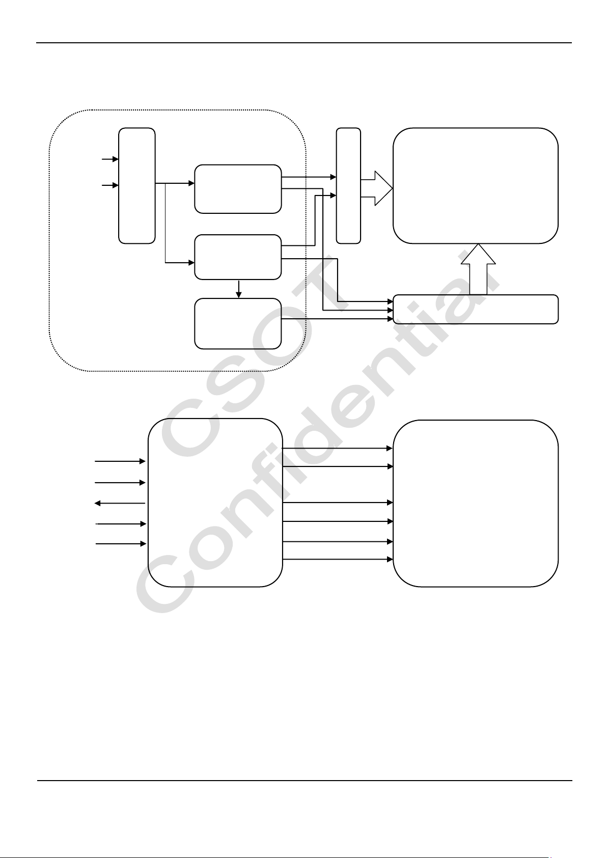
4. Electrical Block Diagram
GAMMA
Voltage
TFT LCD Panel
(1366 x 768 x 3)
Data Driver
DC/DC
Converter
Scan Driver
X + C Board
Timing
Controller
Input Connector
Backlight
Unit
V+
V+
LED
Converter V-
V-
VV-
Converter Connector
V
CC
Data
BLON
GND
VBL
P_DIM
DET
MT3151A05-1 Product Specification
The copyright belongs to Shenzhen China Star 12 / 30 Ver. 2.1
Optoelectronics Technology Co., Ltd.
Any unauthorized use is prohibited.
Page 13

5. Input Terminal Pin Assignment
Pin No.
Symbol
Description
Note
1
VCC
Power Supply ,+ 12 V DC Regulated
2 VCC
Power Supply ,+ 12 V DC Regulated
3 VCC
Power Supply ,+ 12 V DC Regulated
4 VCC
Power Supply ,+ 12 V DC Regulated
5 GND
Ground 6
GND
Ground 7
GND
Ground 8
GND
Ground 9
LVDS SEL
LVDS Data Format Selection
(2)
10
NC
For CSOT internal only
(3)
11
GND
Ground 12
LV1N0
1st Channel LVDS Data Input (0-)
13
LV1P0
1st Channel LVDS Data Input (0+)
14
GND
Ground
15
LV1N1
1st Channel LVDS Data Input (1-)
16
LV1P1
1st Channel LVDS Data Input (1+)
17
GND
Ground 18
LV1N2
1st Channel LVDS Data Input (2-)
19
LV1P2
1st Channel LVDS Data Input (2+)
20
GND
Ground 21
LVCK1N
1st Channel LVDS Clock Input (-)
22
LVCK1P
1st Channel LVDS Clock Input (+)
23
GND
Ground
24
LV1N3
1st Channel LVDS Data Input (3-)
25
LV1P3
1st Channel LVDS Data Input (3+)
26
GND
Ground 27
NC
For CSOT internal only
(3)
28
NC
For CSOT internal only
(3)
29
NC
For CSOT internal only
(3)
30
GND
Ground
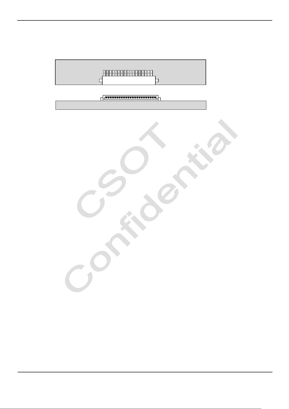
5.1 TFT LCD Module
X + C Board CN1: 300B30-0000RA-M4 (Starconn) or equivalent (see Note (1))
MT3151A05-1 Product Specification
The copyright belongs to Shenzhen China Star 13 / 30 Ver. 2.1
Optoelectronics Technology Co., Ltd.
Any unauthorized use is prohibited.
Page 14
MT3151A05-1 Product Specification
# 1
# 30
# 1
# 30
CN1
CN1
Note:
(1) The direction of pin assignment is shown as below:
Fig. 5.1 LVDS connector direction sketch map
(2) High: connect to + 3.3 V → JEIDA format; Low: connect to GND or Open → VESA format.
(3) For CSOT internal only, please let it open.
The copyright belongs to Shenzhen China Star 14 / 30 Ver. 2.1
Optoelectronics Technology Co., Ltd.
Any unauthorized use is prohibited.
Page 15

5.2 Converter Unit
Pin No.
Symbol
Feature
1
VBL
Power Supply, + 24V DC Regulated
2 3 4 5 6
GND
GND
7
8 9 10
11
DET
Normal (0 ~ 0.8V), Abnormal (Open Collector)
(Recommend Pull high R > 10K, VDD = 3.3V)(Note (2))
12
BLON
Back Light On/ Off
13
NC
No Connection
14
P_DIM
PWM Dimming Control (Open for 100%)
# 1
# 14
CNF1
CNF1
# 1
# 14
5.2.1 Converter Input Connector Pin Definition
Converter Board CNF1: 50308-0140N-002 (ACES) or equivalent (see 4.2 Note (1))
MT3151A05-1 Product Specification
Attention:
If the external PWM function is less than 5% dimming ratio, the judge conditions are as below:
(1) The direction of pin assignment is shown as below.
Fig. 5.2 Converter connector direction sketch map
(2) When open collector occur, the limit current resistor need to be connected to DET pin to prevent MOSFET
from damage, the maximum drain current of MOSFET is 100mA.
The copyright belongs to Shenzhen China Star 15 / 30 Ver. 2.1
Optoelectronics Technology Co., Ltd.
Any unauthorized use is prohibited.
Page 16
MT3151A05-1 Product Specification
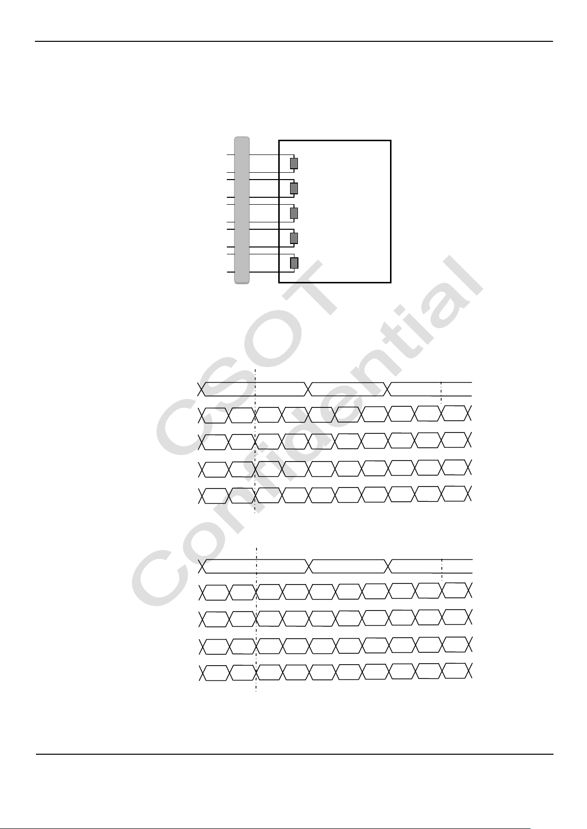
B3 B2 G7 G6 G5 G4 G3
RSVD B1 B0 G1 G0 R1 R0
DE VS HS B7 B6 B5 B4
G2 R7 R6 R5 R4 R3 R2
B1 B0 G5 G4 G3 G2 G1
RSVD B7 B6 G7 G6 R7 R6
DE VS HS B5 B4 B3 B2
G0 R5 R4 R3 R2 R1 R0
LVCK1 N/ LVCK1 P
LV1N0/ LV1P0
LV1N1/ LV1P1
LV1N2/ LV1P2
LV1N3/ LV1P3
Connector
Timing Controller
LVCK1 N/ LVCK1 P
LV1N0/ LV1P0
LV1N1/ LV1P1
LV1N2/ LV1P2
LV1N3/ LV1P3
100Ω
100Ω
100Ω
100Ω
100Ω
LVCK1P
LV1N3
LV1P1
LV1N2
LV1N0
LV1P0
LV1N1
LV1P2
LVCK1N
LV1P3
5.3 Block Diagram of Interface
Attention:
(1) LCD module uses a 100 ohms (Ω) resistor between positive and negative lines of each receiver input.
(2) LVDS cable impedance shall be 50 ohms per signal line or about 100 ohms per twist-pair line respectively.
5.4 LVDS Interface
5.4.1 VESA Format (SELLVDS = L or Open)
5.4.2 JEIDA Format (SELLVDS = H)
The copyright belongs to Shenzhen China Star 16 / 30 Ver. 2.1
Optoelectronics Technology Co., Ltd.
Any unauthorized use is prohibited.
Page 17
MT3151A05-1 Product Specification
Data Input Color
Data Signal
Red
Green
Blue
MSB LSB
MSB LSB
MSB LSB
R7
R6
R5
R4
R3
R2
R1
R0
G7
G6
G5
G4
G3
G2
G1
G0
B7
B6
B5
B4
B3
B2
B1
B0
Basic Colors
Black 0 0 0 0 0 0 0 0 0 0 0 0 0 0 0 0 0 0 0 0 0 0 0 0
Red 1 1 1 1 1 1 1 1 0 0 0 0 0 0 0 0 0 0 0 0 0 0 0 0
Green 0 0 0 0 0 0 0 0 1 1 1 1 1 1 1 1 0 0 0 0 0 0 0 0
Blue 0 0 0 0 0 0 0 0 0 0 0 0 0 0 0 0 1 1 1 1 1 1 1 1
Cyan 0 0 0 0 0 0 0 0 1 1 1 1 1 1 1 1 1 1 1 1 1 1 1 1
Magenta
1 1 1 1 1 1 1 1 0 0 0 0 0 0 0 0 1 1 1 1 1 1 1 1 Yellow
1 1 1 1 1 1 1 1 1 1 1 1 1 1 1 1 0 0 0 0 0 0 0 0 White 1 1 1 1 1 1 1 1 1 1 1 1 1 1 1 1 1 1 1 1 1 1 1 1
Gray Scale of
Red
Red (0) / Dark
0 0 0 0 0 0 0 0 0 0 0 0 0 0 0 0 0 0 0 0 0 0 0 0 Red (1)
0 0 0 0 0 0 0 1 0 0 0 0 0 0 0 0 0 0 0 0 0 0 0
0 : : : : : : : : : : : : : : : : : : : : : : : : : : : : : : : : : : : : : : : : : : : : : : : : : :
Red (254)
1 1 1 1 1 1 1 0 0 0 0 0 0 0 0 0 0 0 0 0 0 0 0 0 Red (255)
1 1 1 1 1 1 1 1 0 0 0 0 0 0 0 0 0 0 0 0 0 0 0
0
Gray Scale of
Green
Green (0) / Dark
0 0 0 0 0 0 0 0 0 0 0 0 0 0 0 0 0 0 0 0 0 0 0 0 Green (1)
0 0 0 0 0 0 0 0 0 0 0 0 0 0 0 1 0 0 0 0 0 0 0
0 : : : : : : : : : : : : : : : : : : : : : : : : : : : : : : : : : : : : : : : : : : : : : : : : : :
Green (254)
0 0 0 0 0 0 0 0 1 1 1 1 1 1 1 0 0 0 0 0 0 0 0
0
Green (255)
0 0 0 0 0 0 0 0 1 1 1 1 1 1 1 1 0 0 0 0 0 0 0
0
Gray Scale of
Blue
Blue (0) / Dark
0 0 0 0 0 0 0 0 0 0 0 0 0 0 0 0 0 0 0 0 0 0 0 0 Blue (1)
0 0 0 0 0 0 0 0 0 0 0 0 0 0 0 0 0 0 0 0 0 0 0
1 : : : : : : : : : : : : : : : : : : : : : : : : : : : : : : : : : : : : : : : : : : : : : : : : : :
Blue (254)
0 0 0 0 0 0 0 0 0 0 0 0 0 0 0 0 1 1 1 1 1 1 1 0 Blue (255)
0 0 0 0 0 0 0 0 0 0 0 0 0 0 0 0 1 1 1 1 1 1 1
1
5.5 Color Data Input Assignment
The brightness of each primary color is based on the 8-bit gray scale data input for each color. The higher the binary input,
the brighter the color. The table below provides the assignment of the color versus.
Attention:
0: Low level voltage; 1: High level voltage.
The copyright belongs to Shenzhen China Star 17 / 30 Ver. 2.1
Optoelectronics Technology Co., Ltd.
Any unauthorized use is prohibited.
Page 18

6. Interface Timing
Signal
Item
Symbol
Min.
Typ.
Max.
Unit
Note
LVDS Clock
Frequency
F
CLK
(= 1 / T
CLK
)
50.0
75.4
85.0
MHz
Vertical
Term
Frame Rate
F
47.0
60.0
63.0
Hz
Vertical Frequency
FV
47.0
48.4
60.9
KHz
Total
TV
784.0
806.0
1015.0
TH
TV = TVD + TVB
Display
TVD
768.0
TH
Blank
TVB
16.0
38.0
247.0
TH
Horizontal
Term
Total
TH
1460.0
1560.0
2000.0
T
CLK
TH = THD+ THB
Display
THD
1366.0
T
CLK
Blank
THB
94.0
194.0
634.0
T
CLK
TVD
TVB
TV
TH
DE
THB
Valid Display Data
T
CLK
DCLK
THD
DE
DATA
6.1 Timing Table (DE Only Mode)
MT3151A05-1 Product Specification
Attention:
(1) The module is operated in DE only mode, H sync and V sync input signal have no effect on normal operation.
Fig. 6.1 Interface signal timing diagram
The copyright belongs to Shenzhen China Star 18 / 30 Ver. 2.1
Optoelectronics Technology Co., Ltd.
Any unauthorized use is prohibited.
Page 19
MT3151A05-1 Product Specification
Fig. 6.2 Power On/Off Sequence
LVDS & Option Signal
BLU On/Off
Parameter
Values
Unit
Min.
Typ.
Max.
T1
0.5 - 10
ms
T2 0 - - ms
T3 0 - - ms
T4
1000 - -
ms
T5
500 - -
ms
T6
100 - -
ms
50%
T6
0.1 VCC
Power Off
50%
T5
T4
0 V
0 V
T3
T1
0.1 VCC
T2
Valid Data
Power On
6.2 Power On/Off Sequence
To prevent a latch-up or DC operation of LCD module, the power on/off sequence should be as the diagram below.
Attention:
(1) The supply voltage of the external system for the module input should follow the definition of VCC.
(2) Apply the lightbar voltage within the LCD operation range. When the backlight turns on before the LCD operation or the
LCD turns off before the backlight turns off, the display may momentarily become abnormal screen.
(3) In case that VCC is in off level, please keep the level of input signals on the low or high impedance. If T2 < 0, that may
cause electrical overstress.
(4) T4 should be measured after the module has been fully discharged between power off and on period.
(5) Interface signal shall not be kept at high impedance when the power is on.
The copyright belongs to Shenzhen China Star 19 / 30 Ver. 2.1
Optoelectronics Technology Co., Ltd.
Any unauthorized use is prohibited.
Page 20
7. Optical Characteristics
Item
Symbol
Value
Unit
Ambient Temperature
TA
25 2
ºC
Ambient Humidity
HA
50 10
% RH
LVDS Supply Voltage
VCC
12
V
Driving Signal
Refer to the typical value in Chapter 3: Electrical Specification
LED Driving Current
IL
120
mA
Vertical Refresh Rate
FR
60
Hz
r
S = πr²
For Square
Z
Z
≥ 500pixels
N means the actual number of the pixels in the area S.
N =
S
A
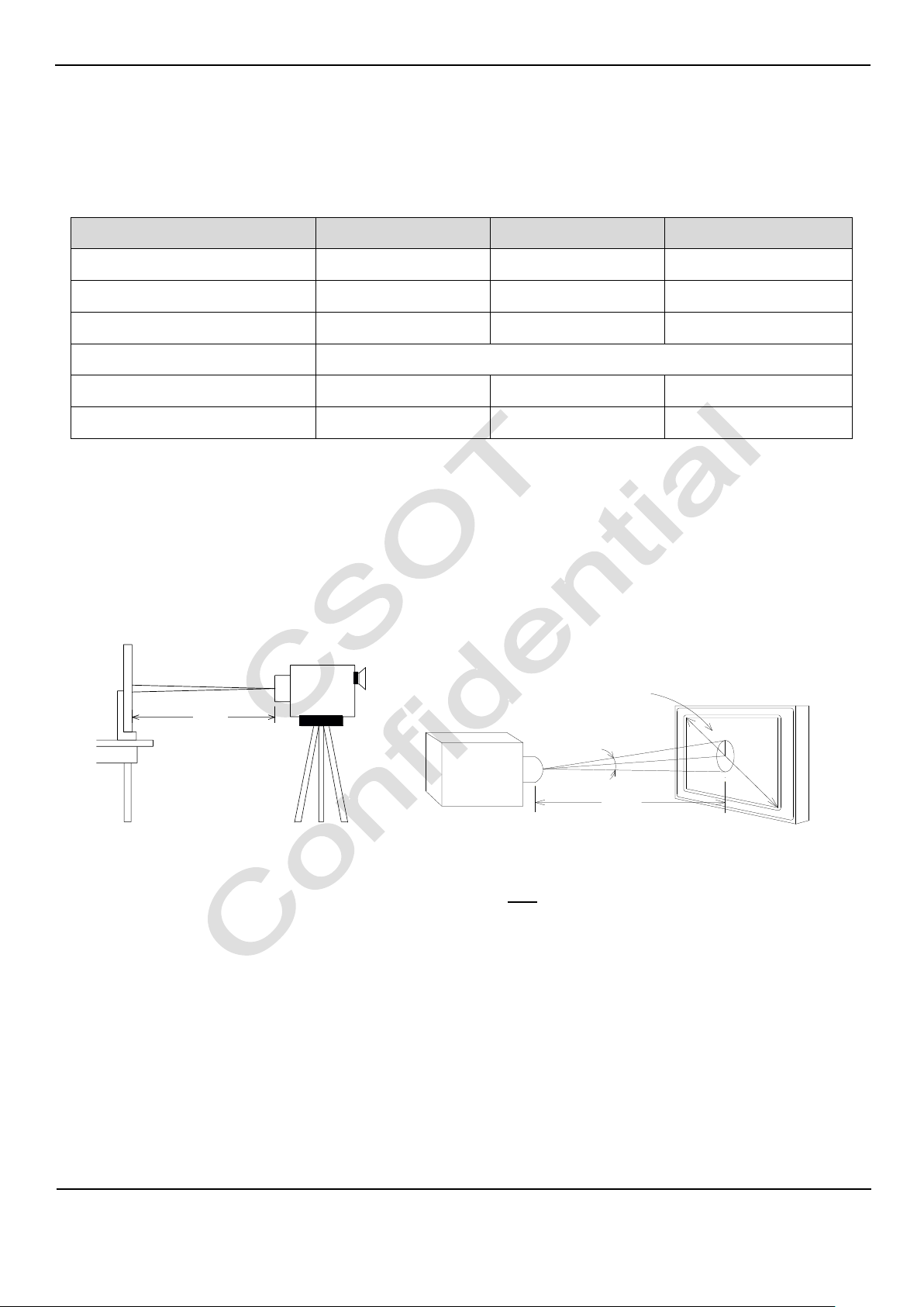
7.1 Measurement Conditions
The table below is the test condition of optical measurement.
To avoid abrupt temperature change during optical measurement, it’s suggested to warm up the LCD module more than 45
minutes after lighting the backlight and in the windless environment.
MT3151A05-1 Product Specification
To measure the LCD module, it is suggested to set up the standard measurement system as Fig. 7.1. The measuring area S
should contain at least 500 pixels of the LCD module as illustrated in Fig. 7.2 (A means the area allocated to one pixel). In this
model, for example, the minimum measuring distance Z is 370 mm when is 2 degree. Hence, 500 mm is the typical
measuring distance. This measuring condition is referred to 301-2H of VESA FPDM 2.0 about viewing distance, angle, and
angular field of view definition.
Fig. 7.1 The standard set-up system of measurement
Fig. 7.2 The area S contains at least 500 pixels to be measured
The copyright belongs to Shenzhen China Star 20 / 30 Ver. 2.1
Optoelectronics Technology Co., Ltd.
Any unauthorized use is prohibited.
Page 21
MT3151A05-1 Product Specification
Item
Symbol
Condition
Min.
Typ.
Max.
Unit
Note
Static Contrast Ratio
CR
H
= 0, V = 0
Normal direction at
center point of the
LCD Module
2400
3000 - -
(1) (2)
Response Time
TL - 6.5
12
ms
(3)
Center Luminance
LW
250
300
-
cd/m2
(2) (4)
Uniformity of White Screen
-
70 - - % (2) (5)
Color
Chromaticity
(CIE1931)
Red
RX
Typ.
- 0.03
0.613
Typ.
+ 0.03
-
(2) (6)
RY
0.333
-
Green
GX
0.331
-
GY
0.604
-
Blue
BX
0.153
-
BY
0.071
-
White
WX
0.274
-
WY
0.292
-
Color Gamut
CG - 62
-
% NTSC
Viewing Angle
Horizontal
H+
CR 10
80
89
-
Deg.
(7)
H-
80
89
-
Vertical
V+
80
89
-
V-
80
89
-
CR-W
CR-D
7.2 Optical Specifications
The table below of optical characteristics is measured by MINOLTA CS2000, MINOLTA CA310, ELDIM OPTI
Scope-SA and ELDIM EZ Contrast in dark room.
Note:
(1) Definition of static contrast ratio (CR):
It’s necessary to switch off all the dynamic and dimming function when measuring the static contrast ratio.
Static Contrast Ratio (CR) =
CR-W is the luminance measured by LMD (light-measuring device) at the center point of the LCD module with
full-screen displaying white. The standard setup of measurement is illustrated in Fig. 7.3; CR-D is the luminance measured
by LMD at the center point of the LCD module with full-screen displaying black. The LMD in this item is CS2000.
(2) The LMD in the item could be a spectroradiometer such as (KONICA MINOLTA) CS2000, CS1000(TOPCON), SR-UL2
or the same level spectroradiometer. Other display color analyzer (KONICA MINOLTA) CA210, CA310 or (TOPCON)
BM-7 could be involved after being calibrated with a spectroradiometer on each stage of a product.
The copyright belongs to Shenzhen China Star 21 / 30 Ver. 2.1
Optoelectronics Technology Co., Ltd.
Any unauthorized use is prohibited.
Page 22

MT3151A05-1 Product Specification
Measured
Transition Time
Luminance Ratio of Previous Frame
0%
25%
50%
75%
100%
Luminance
Ratio of
Current Frame
0%
t
25% to 0%
t
50% to 0%
t
75% to 0%
t
100% to 0%
25%
t
0% to 25%
t
50% to 25%
t
75% to 25%
t
100% to 25%
50%
t
0% to 50%
t
25% to 50%
t
75% to 50%
t
100% to 50%
75%
t
0% to 75%
t
25% to 75%
t
50% to 75%
t
100% to 75%
100%
t
0% to 100%
t
25% to 100%
t
50% to 100%
t
75% to 100%
100%
90%
10%
0%
Time
Luminance
t
X to Y
Y: 0%, 25% 50%, 75%, 100%
X: 0%, 25% 50%, 75%, 100%
Brighter state
Darker state
Y: 0%, 25%, 50%, 75%, 100%
t
X to Y
100%
Brighter State
10%
0%
Time
Luminance
X: 0%, 25%, 50%, 75%, 100%
Darker State
Black & White
LCD Module
LMD
90%
Fig. 7.3 The standard setup of CR measurement
(3) Response time TL is defined as the average transition time in the response time matrix. The table below is the response
time matrix in which each element t
luminance ratios among 0%, 25%, 50%, 75%, and 100% luminance. The transition time t
is the transition time from luminance ratio X to Y. X and Y are two different
X to Y
is defined as the time taken
X to Y
from 10% to 90% of the luminance difference between X and Y (X < Y) as illustrated in Fig.7.4. When X > Y, the
definition of t
is the time taken from 90% to 10% of the luminance difference between X and Y. The response time is
X to Y
optimized on refresh rate Fr = 60Hz.
t
means the transition time from luminance ratio X to Y.
X to Y
All the transition time is measured at the center point of the LCD module by ELDIM OPTI Scope-SA.
The copyright belongs to Shenzhen China Star 22 / 30 Ver. 2.1
Optoelectronics Technology Co., Ltd.
Any unauthorized use is prohibited.
Fig. 7.4 The definition of t
X to Y
Page 23
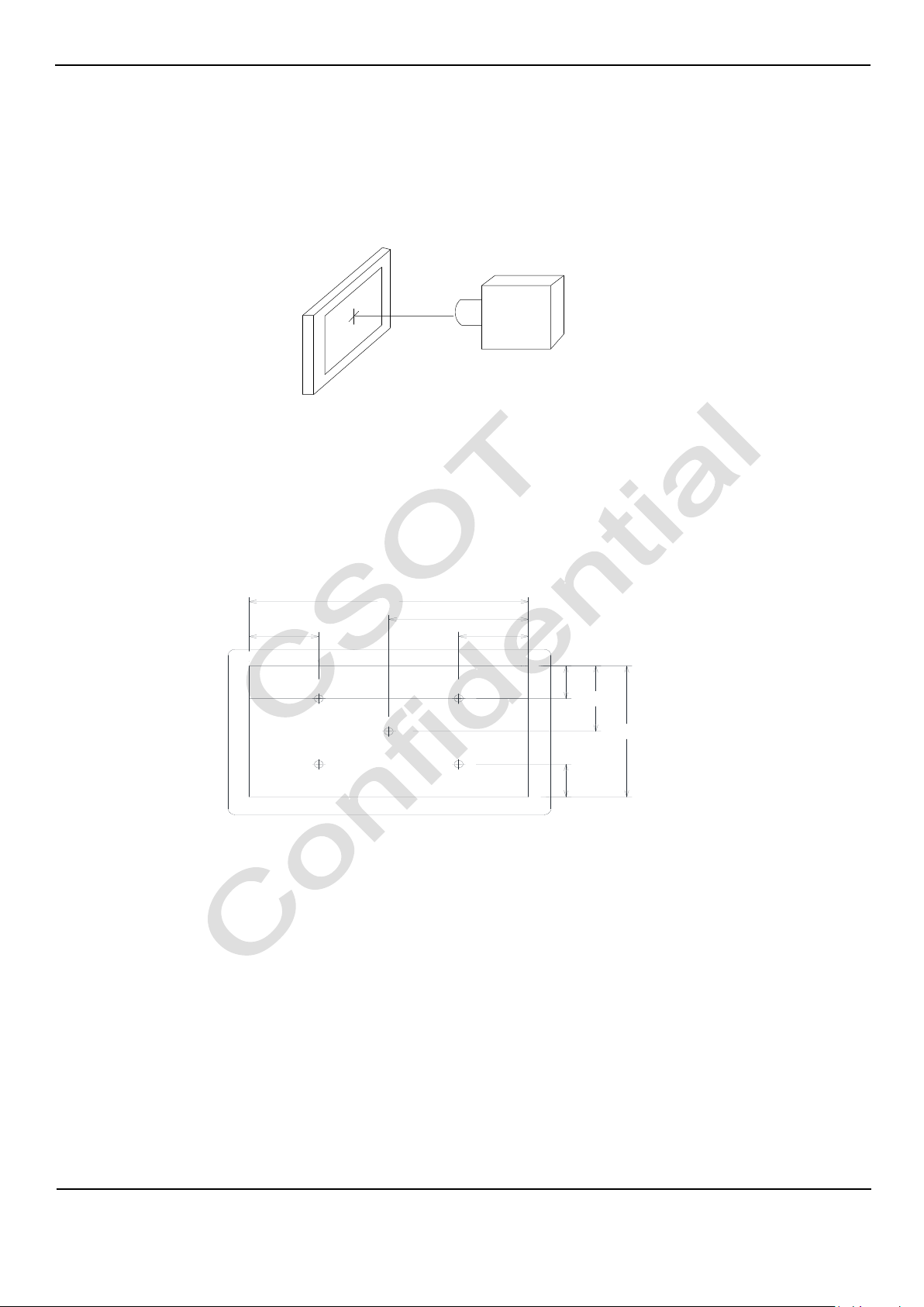
(4) Definition of center luminance (LW):
White
LCD Module
LMD
V/2
V
H/2
H
H/4
H/4
V/4
V/4
(1)
(4)
(3)
(2)
(5)
The luminance is measured at the center point of the LCD module with full-screen displaying white. Fig. 7.5 shows the
standard setup of luminance measurement.
Fig. 7.5 The standard setup of luminance measurement
(5) Definition of uniformity of white screen:
The luminance Li (i from 1 to 5) is measured at the 5 points defined in Fig. 7.6. H and V indicate active area.
MT3151A05-1 Product Specification
From the measured set of luminance values Li (i from 1 to 5), the minimum luminance is denoted as L
maximum luminance is denoted as L
Uniformity = L
min
/ L
x 100%.
max
. The uniformity of white screen is defined according to
max.
and the
min
Fig. 7.6 Symbol “ + ” defines the 5 measuring locations (1), (2), (3) ··· (5)
(6) Definition of color chromaticity:
Each chromaticity coordinates (x, y) are measured in CIE1931 color space when full-screen displaying primary color R, G,
B and white. The color gamut is defined as the fraction in percent of the area of the triangle bounded by R, G, B
coordinates and the area is defined by NTSC 1953 color standard in the CIE color space. Chromaticity coordinates are
measured by CS2000 and the standard setup of measurement is shown in Fig. 7.7.
The copyright belongs to Shenzhen China Star 23 / 30 Ver. 2.1
Optoelectronics Technology Co., Ltd.
Any unauthorized use is prohibited.
Page 24

MT3151A05-1 Product Specification
Colors
LCD Module
LMD
H+
H-
V-
V+
Z Y X
Fig. 7.7 The standard setup of color chromaticity measurement
(7) Definition of viewing angle coordinate system (H, V):
The contrast ratio is measured at the center point of the LCD module. The viewing angles are defined at the angle that the
contrast ratio is larger than 10 at four directions relative to the perpendicular direction of the LCD module (two vertical
angles: up V+ and down V-; and two horizontal angles: right H+ and left H-) as illustrated in Fig. 7.8. The contrast ratio
is measured by ELDIM EZ Contrast.
Fig. 7.8 Viewing angle coordination system
The copyright belongs to Shenzhen China Star 24 / 30 Ver. 2.1
Optoelectronics Technology Co., Ltd.
Any unauthorized use is prohibited.
Page 25

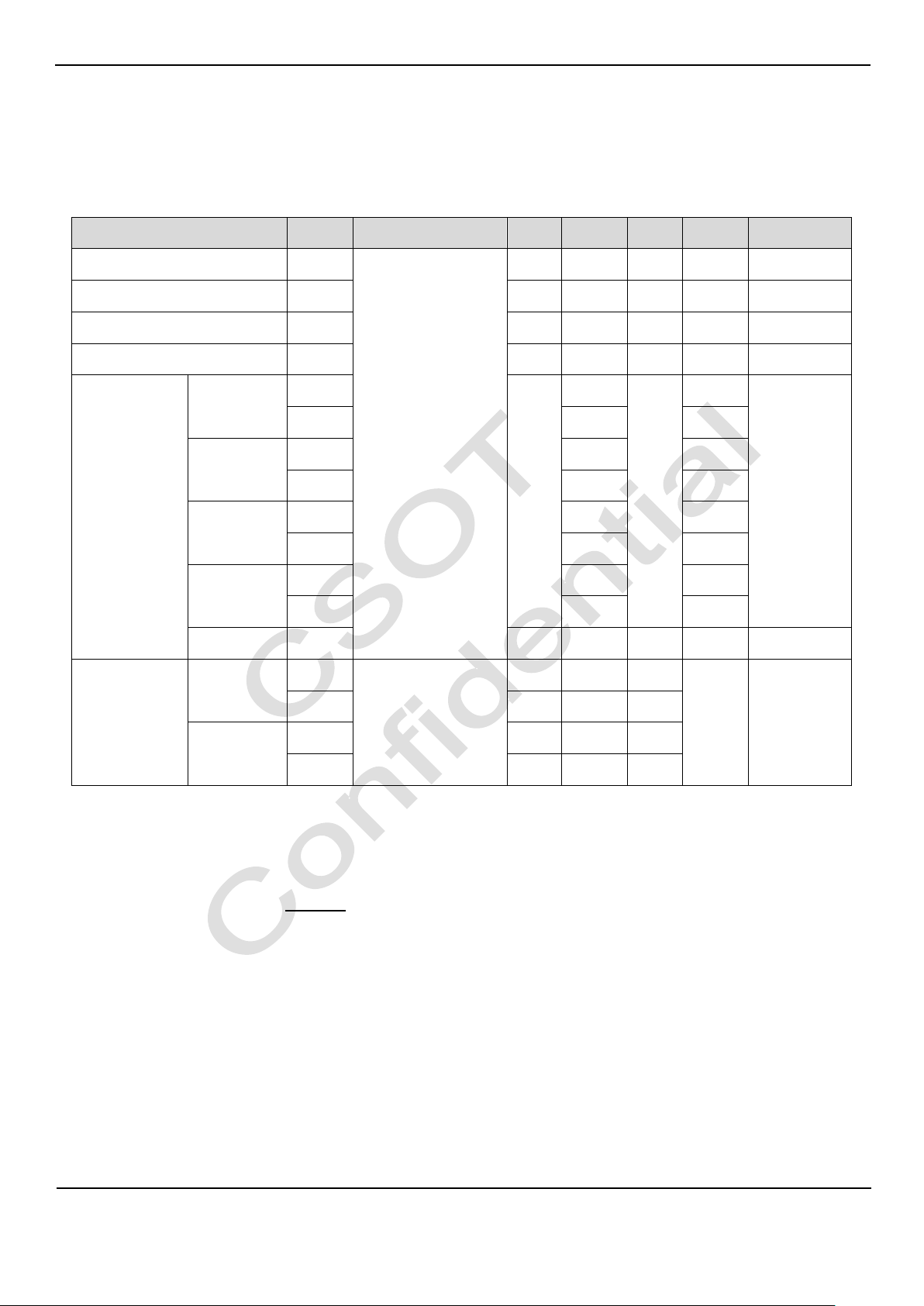
8. Mechanical Characteristics
8.1 Mechanical Specification
MT3151A05-1 Product Specification
The copyright belongs to Shenzhen China Star 25 / 30 Ver. 2.1
Optoelectronics Technology Co., Ltd.
Any unauthorized use is prohibited.
Page 26

MT3151A05-1 Product Specification
The copyright belongs to Shenzhen China Star 26 / 30 Ver. 2.1
Optoelectronics Technology Co., Ltd.
Any unauthorized use is prohibited.
Page 27
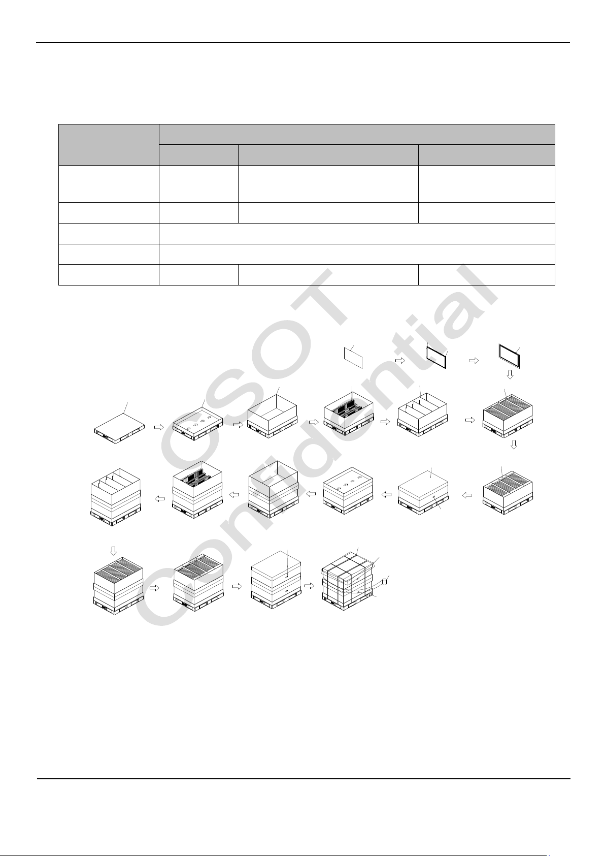
8.2 Packing
Item
Specification
Quantity
Dimension (mm)
Weight (kg)
Packing Box
24 pcs / box
1140.00 (L) x 818.00 (W) x 505.00 (H)
Net Weight: 103.20(Max.)
Gross Weight: 112.00 (Max.)
Pallet
1
1150.00 (L) x 850.00 (W) x 120.00 (H)
Net Weight:5.04
Stack Layer
2
Boxes per Pallet
2 boxes / pallet
Pallet after Packing
48 pcs / pallet
1150.00 (L) x 850.00 (W) x 1130.00(H)
Gross Weight:230.00
Protector Film
Bottom Cushion (2pcs)
PE Bag
Top Cushion (2pcs)
Board (3pcs)
Carton Label (2pcs)
PP Belt
PE Film
Pallet Label (2pcs)
Around Box
PE Sheet
Pallet
Masking Tape
LCD TV Module (24pcs)
Earth Box
Heaven Box
Carton Label (2pcs)
8.2.1 Packing Specifications
8.2.2 Packing Method
MT3151A05-1 Product Specification
The copyright belongs to Shenzhen China Star 27 / 30 Ver. 2.1
Optoelectronics Technology Co., Ltd.
Any unauthorized use is prohibited.
Fig. 8.1 Packing method (protector film stick on the front of the LCD module)
Page 28
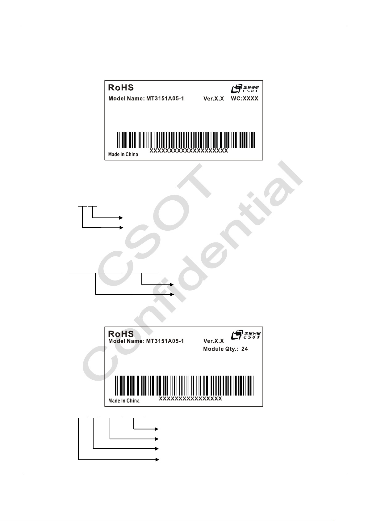
9. Definition of Labels
CSOT Internal Use
Model Version Code
Year, Month, Date
CSOT Internal Use
CSOT Internal Use
Panel ID
Week
Year
9.1 Module Label
For RoHS compliant products, CSOT will add RoHS for identification.
Model Name: MT3151A05-1
Ver. X.X: Version, for example: 0.1, 0.2, … , 1.1, 1.2, …, 2.1, 2.2, …
MT3151A05-1 Product Specification
WC (Week Code): XX XX
Year: 2010 = 10, 2011 = 11 … 2020 = 20, 2021 = 21…
Week: 01, 02, 03 …
Serial Number: XXXXXXXXXXXX XXXXXXXX
9.2 Carton Label
Serial Number: XXXX XX XXXXX XXXXX
The copyright belongs to Shenzhen China Star 28 / 30 Ver. 2.1
Optoelectronics Technology Co., Ltd.
Any unauthorized use is prohibited.
Page 29

Manufactured Date:
CSOT Internal Use
Model Version Code
Year, Month
CSOT Internal Use
Made In China
Model Name: MT3151A05-1
Module Qty.: 48
Ver. X.X
Note:
Carton Qty.: 2
Year: 2010 = 10, 2011 = 11…2020 = 20, 2021 = 21…
Month: 1~9, A~C, for Jan. ~ Dec.
Date: 01~31, for 1st to 31st
Model Version Code: Version of product, for example: 01, 02, 11, 12…
9.3 Pallet Label
MT3151A05-1 Product Specification
Serial Number: XXX XX XXX XXXXX
The copyright belongs to Shenzhen China Star 29 / 30 Ver. 2.1
Optoelectronics Technology Co., Ltd.
Any unauthorized use is prohibited.
Page 30

MT3151A05-1 Product Specification
10. Precautions
10.1 Assembly and Handling Precautions
(1) Do not apply rough force such as bending or twisting to the module during assembly.
(2) It is recommended to assemble or install a module into the user’s system in clean working areas. The dust and oil
may cause electrical short or damage the polarizer.
(3) Do not apply pressure or impulse to the module to prevent the damage to LCD panel and backlight.
(4) Always follow the correct power-on sequence. This can prevent the damage and latch-up to the LSI chips.
(5) Do not plug in or pull out the interface connector while the module is in operation.
(6) Do not disassemble the module.
(7) Use soft dry cloth without chemicals for cleaning because the surface of polarizer is very soft and easily be
scratched.
(8) Moisture can easily penetrate into the LCD module and may cause the damage during operation.
(9) High temperature or humidity may deteriorate the performance of the LCD module. Please store LCD modules in
the specified storage conditions.
(10) When ambient temperature is lower than 10 ºC, the display quality might be deteriorated. For example, the
response time will become slow, and the starting voltage of LED light bar will be higher than that in room
temperature.
10.2 Safety Precautions
(1) If the liquid crystal material leaks from the panel, it should be kept away from the eyes or mouth. In case of
contact with hands, skin or clothes, it has to be washed away thoroughly with soap.
(2) After the module’s end of life, it is not harmful in case of normal operation and storage.
The copyright belongs to Shenzhen China Star 30 / 30 Ver. 2.1
Optoelectronics Technology Co., Ltd.
Any unauthorized use is prohibited.
 Loading...