查询CS5126-KL供应商查询CS5126-KL供应商
16-Bit, Stereo A/D Converter for Digital Audio
CS5126
Features
l Monolithic CMOS A/D Converter
- Inherent Sampling Architecture
- Stereo or Monaural Capability
- Serial Output
l Monaural Sampling Rates up to 100 kHz
- 50 kHz/Channel Stereo Sampling
l Signal-to-(N o ise + Dis to r ti on) : 92 dB
l Dynamic Range: 92 dB
- 95 dB in 2X Oversampling Schemes
l Interchannel Isolation: 90 dB
l 2’s Complement or Binary Coding
l Low Power Dissipation: 260 mW
- Power Down Mode for Portable Applications
l Evaluation Board Available
I
Description
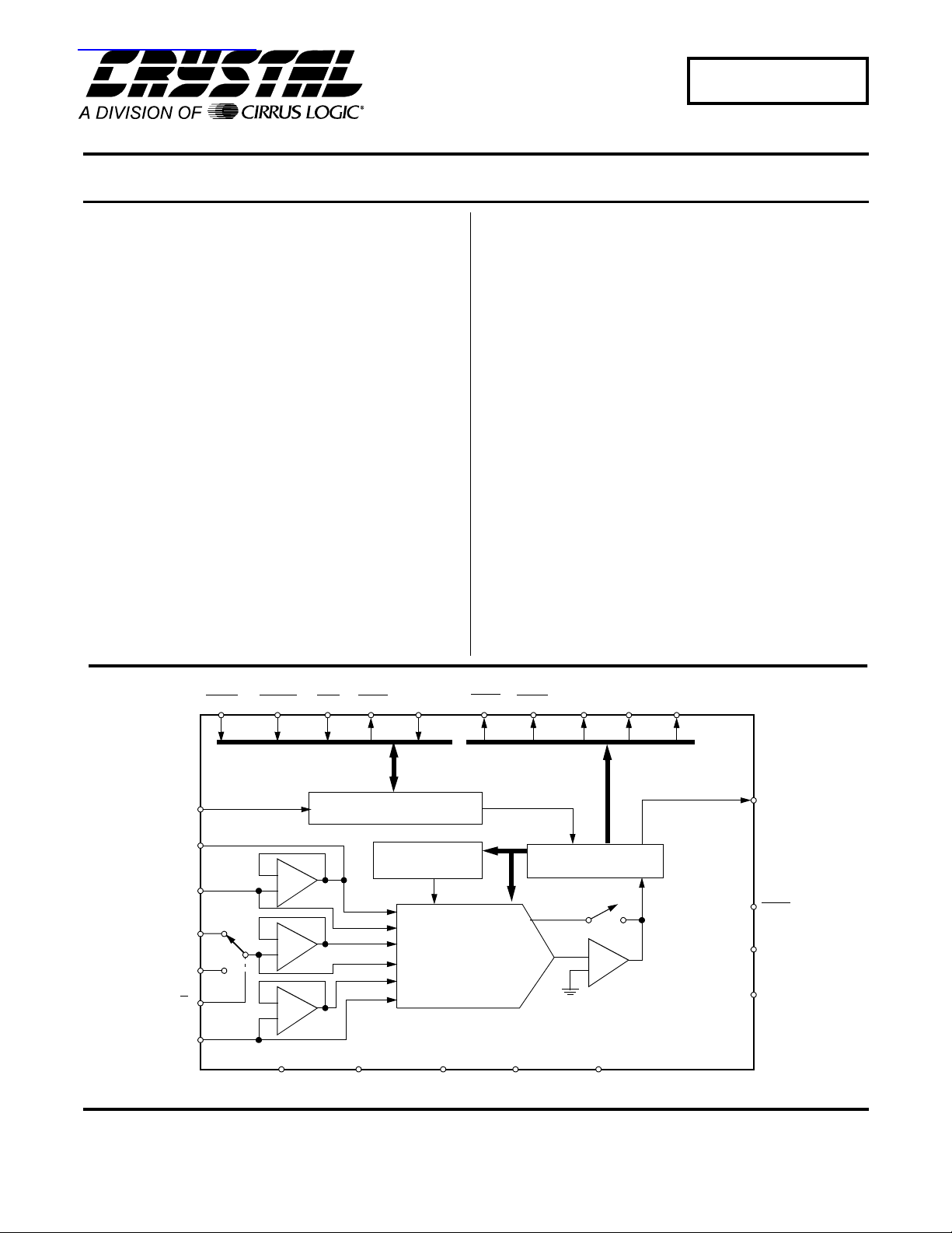
The CS5126 CMOS analog-to-digital converter is an ideal front-end for stereo or monaural digital audio systems.
The CS5126 can be c onfigur ed to han dle two c hannels
at up to 50 kHz sam pling per channe l, or it can be co nfigured to sample one channel at rates up to 100 kHz.
The CS5126 executes a successive approximation algorithm using a charge redistribution architecture. On-chip
self-calibration ci rcui tr y h as 18- bi t re so lu tion thus av oi ding any degradation in performance with low-level
signals. The charge redistribution technique also provides an inherent sampling function which avoids the
need for external sample/hold amplifiers.
Signal-to-(noise+distortion) in stereo operation is 92 dB,
and is dominated by int ernal broad band nois e (1/2 LSB
rms). When the CS5126 is config ured for 2X oversampling, digital pos t-filtering bandlimits th is white noise to
20 kHz, increasing dynamic range to 95 dB.
ORDERING INFORMATION
CS5126-KP 0° to 70° C 28-pin Plastic DIP
CS5126-KL 0° to 70° C 28-pin PLCC
+2/' 6/((3 567 &2'(
$,1/
$,15
/5
&/.,1
5()%8)
95()
$*1'
Cirrus Logic, Inc.
Crystal Semiconductor Products Division
P.O. Box 17847, Austin, Texas 78760
(512) 445 7222 FAX: (512) 445 7581
http://www.crystal.com
67%<
&RQWURO
&DOLEUDWLRQ
65$0
%LW&KDUJH
5HGLVWULEXWLRQ
'*1' 9' 9'9$9$
75./
75.5
'$&
Copyright Cirrus Logic, Inc. 1997
(All Rights Reserved)
66+
66+
0LFURFRQWUROOHU
&RPSDUDWRU
6' $7$
6&/.
7(67
6&.02'
28702'
MAR ‘95
DS32F1
1
CS5126
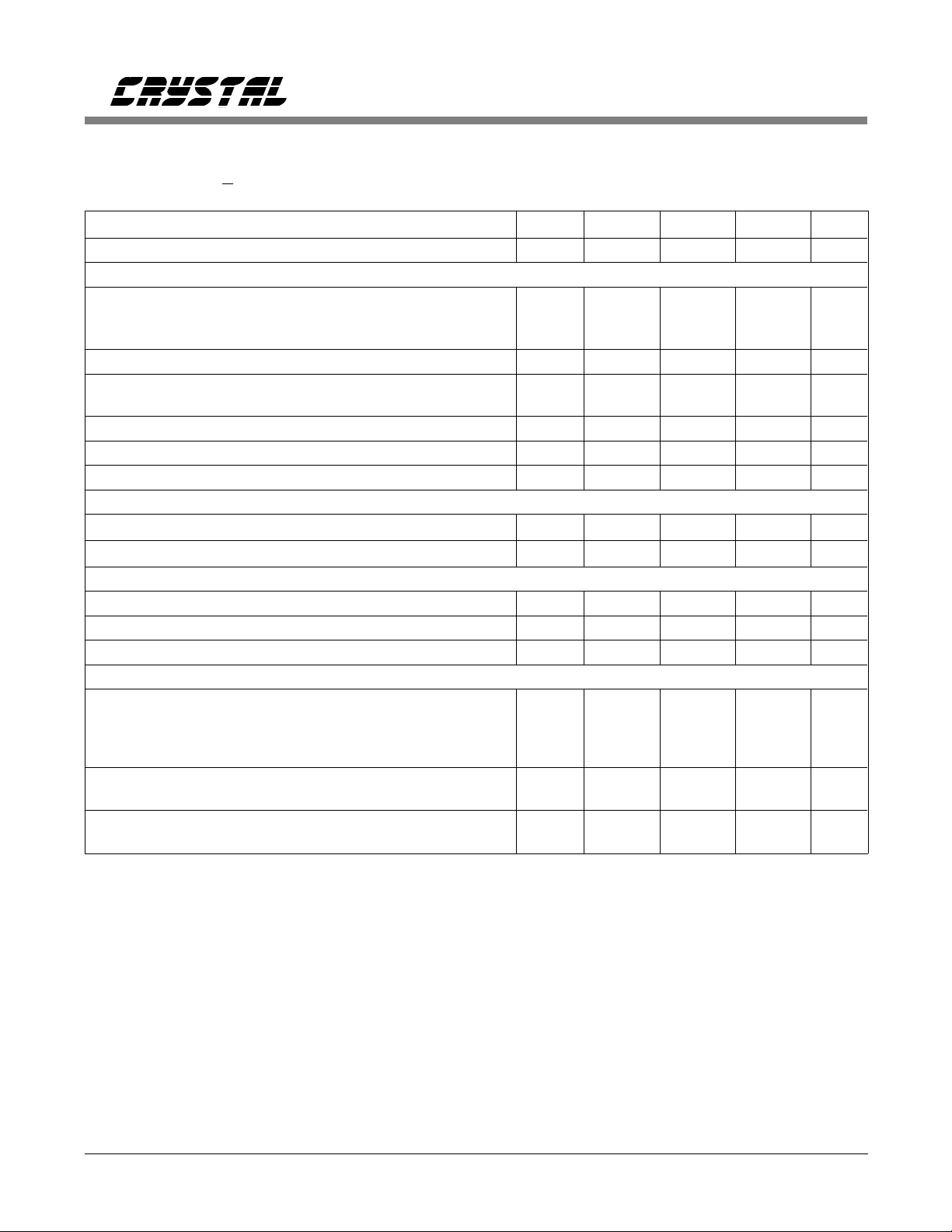
ANALOG CHARACTERISTICS
Full-Scale Input Sinewave, 1kHz; f
Stereo operation, L/
R toggling at 48 kHz unless otherwise specified.)
= 24.576MHz; VREF = 4.5V ; Analog Source Impedance = 200Ω;
clk
(TA = 25°C; VA+, VD+ = 5V; VA-, VD- = -5V;
Parameter* Symbol Min Typ Max Units
Resolution - - 16 Bits
Dynamic Performance
Signal-to-(Noise plus Distortion)
VIN = ±FS (10 Hz to 20 kHz)
VIN = -20dB (f = 20 kHz)
S/(N+D)
90
70
92
72
-
-
dB
dB
Total Harmonic Distortion THD - 0.001 - %
Dynamic Range Stereo Mode
Monaural (20 kHz BW)
Idle Channel Noise V
Interchannel Isolation (Note 1) I
Interchannel Mismatch M
DR 90
n(ic)
ic
ic
88 90 - dB
92
-
95
-
-
dB
dB
-1/2-LSB
-0.01-dB
dc Accuracy
Full-Scale Error FSE Bipolar Offset Error BPO -
±
4
±
4
-LSB
-LSB
Analog Input
Aperture Time t
Aperture Jitter t
Input Capacitance (Note 2) C
apt
ajt
in
-30-ns
- 100 - ps
- 200 - pF
Power Supplies
Power Supply Current Positive Analog (Note 3)
Negative Analog
(SLEEP High) Positive Digital
Negative Digital
Power Dissipation (SLEEP High) (Notes 3, 4)
(SLEEP Low)
Power Supply Rejection Positive S upplies (Note 5)
Negative Supplies
I
A+
I
A-
I
D+
I
D-
P
do
P
ds
PSR -
-
-
-
-
-
-
-
18
-18
8
-8
260
1
84
84
23
-23
12
-12
350
-
-
-
mA
mA
mA
mA
mW
mW
dB
dB
Notes: 1. One input grounded; dc to 20kHz, Full Scale input on the other channel.
Guaranteed by characterization.
2. Applies only in the track mode. When converting or calibrating, input capacitance will typically
be 10 pF.
3. All outputs unloaded. All inputs CMOS levels .
4. Power dissipation in sleep mode applies with no master clock applied (CLKIN high or low).
5. With 300mV p-p, 1kHz ripple applied to each supply separately. A plot of typical power supply
rejection appears in the
Analog Circuit Connections
section.
rms
* Refer to
Parameter Definitions
at the end of this data sheet.
Specifications are subject to change without notice.
2 DS32F1
CS5126
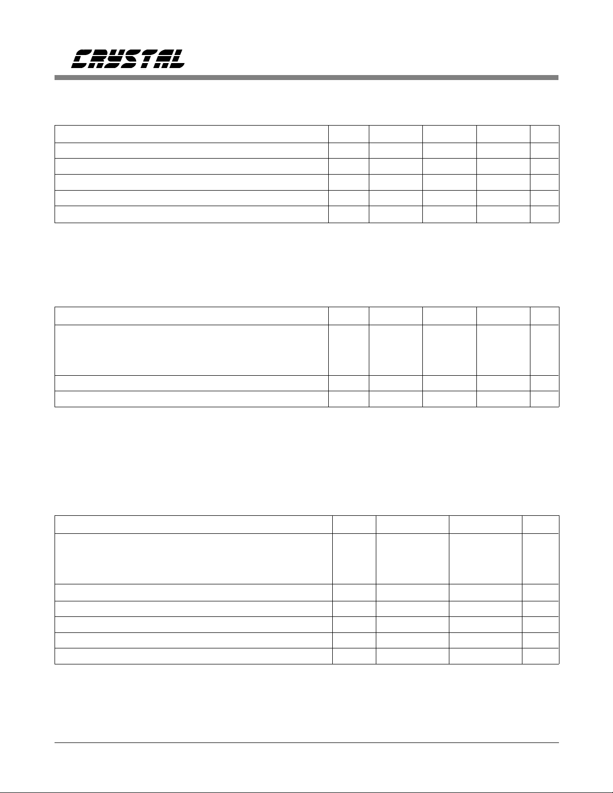
DIGITAL CHARACTERISTICS
(TA = T
MIN
to T
; VA+, VD+ = 5V±10%; VA-,VD - = -5V±10%)
MAX
Parameter Symbol Min Typ Max Units
High-Level Input Voltage V
Low-Level Input Voltage V
High-Level Output Voltage (Note 6) V
Low-Level Output Voltage I
= 1.6 mA V
out
Input Leakage Current I
Notes: 6. I
= -100 µA. This specification guarantees that each digital output will drive one TTL load
OUT
(V
= 2.4V @ I
OH
= -40 µA).
OUT
IH
IL
OH
OL
in
2.0 - - V
--0.8V
(VD+)-1.0V - - V
--0.4V
--10
RECOMMENDED OPERATING CONDITIONS (AGND, DGND = 0V, see note 7.)
Parameter Symbol Min Typ Max Units
DC Power Supplies: Positive Digital
Negative Digital
Positive Analog
Negative Analog
Analog Reference Voltage VREF 2.5 4.5 (VA+)-0.5 V
Analog Input Voltage (Note 8) V
Notes: 7. All voltages with respect to ground.
8. The CS5126 can accept input voltages up to the analog supplies (VA+, VA-). It will produce an
output of all 1’s for inputs above VREF and all 0’s for inputs below -VREF.
VD+
VD-
VA+
VA-
AIN
4.5
-4.5
4.5
-4.5
5.0
-5.0
5.0
-5.0
VA+
-5.5
5.5
-5.5
-VREF - VREF V
µ
A
V
V
V
V
ABSOLUTE MAXIMUM RATINGS (AGND, DGND = 0V, all voltages with respect to ground.)
Parameter Symbol Min Max Units
DC Power Supplies: Positive Digital
Negative Digital
Positive Analog
Negative Analog
Input Current, Any Pin Except Supplies (Note 9) I
Analog Input Voltage (AIN and VREF pins) V
Digital Input Voltage V
Ambient Temperature (power applied) T
Storage Temperature T
Notes: 9. Transient currents of up to 100 mA will not cause SCR latch-up.
WARNING: Operation at or beyond these limits may result in permanent damage to the device.
Normal operation is not guaranteed at these extremes.
DS32F1 3
VD+
VD-
VA+
VA-
in
INA
IND
A
stg
-0.3
0.3
-0.3
0.3
-
(VA+)+0.3
-6.0
6.0
-6.0
±10
mA
(VA-)-0.3 (VA+)+0.3 V
-0.3 (VD+)+0.3 V
-55 125 °C
-65 150 °C
V
V
V
V
CS5126
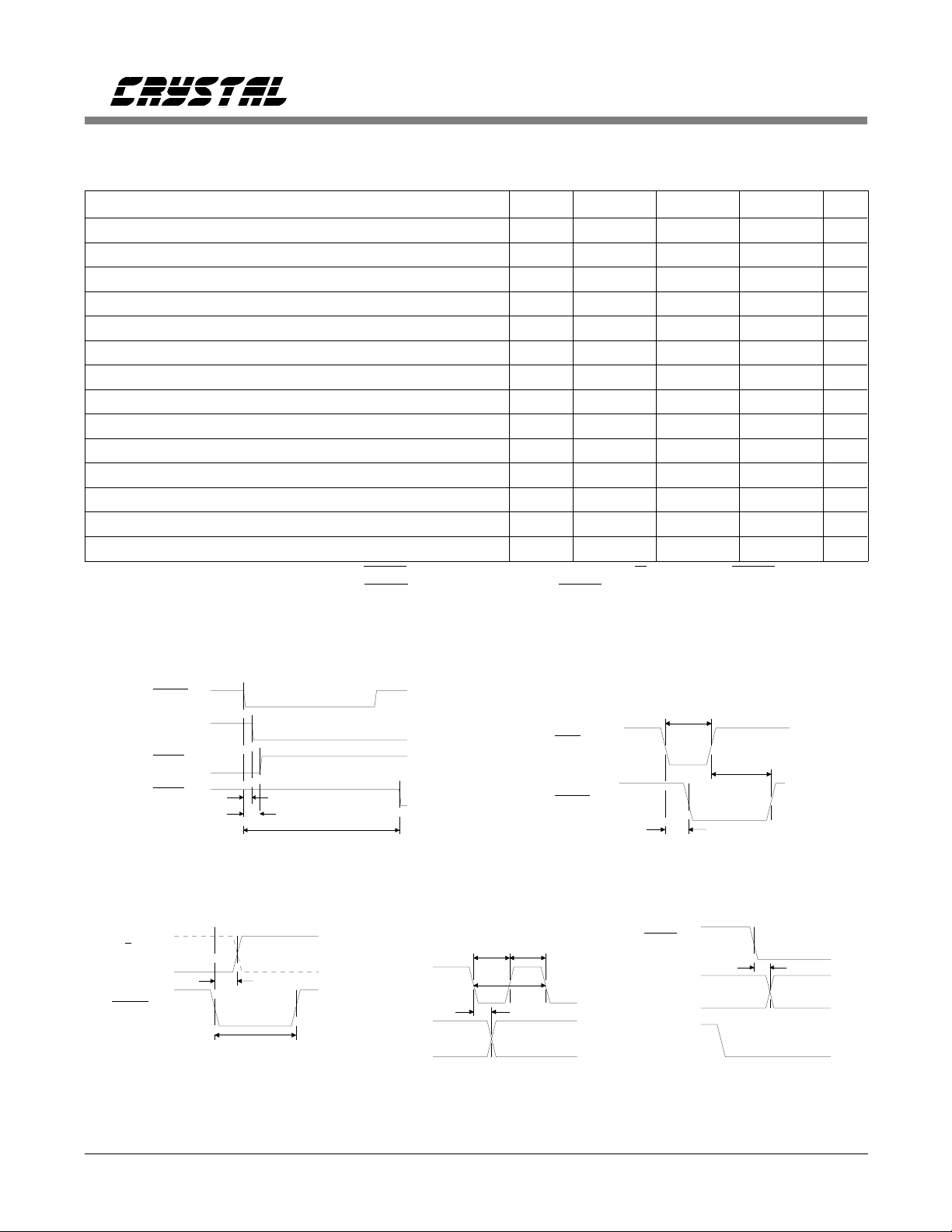
SWITCHING CHARACTERISTICS
Inputs: Logic 0 = 0V, Logic 1 = VD+; C
= 50 pF)
L
(TA = 25 °C; VA+, VD+ = 5V ± 10%; VA-, VD- = -5V ± 10%;
Parameter Symbol Min Typ Max Units
Master Clock Period t
HOLD to SSH2 Falling (Note 10) t
HOLD to TRKL, TRKR SSH1 Falling t
HOLD to TRKL, TRKR SSH1, SSH2 Rising t
RST Pulse Width t
RST to STBY Falling t
RST Rising to STBY Rising t
HOLD Pulse Width t
HOLD to L/R Edge (Note 10) t
SCLK period t
SCLK Pulse Width Low t
SCLK Pulse Width High t
SCLK Falling to SDATA Valid t
HOLD Falling to SDATA Valid t
Notes: 10. SSH2 only works correctly if
occurs between 30ns before
HOLD falling edge is within ±30ns of L/R edge OR if HOLD falling edge
HOLD rises to 192 t
clk
clk
dfsh2
dfsh1
drsh
rst
drrs
cal
hold
dhlri
sclk
sclkl
sclkh
dss
dhs
40 - - ns
-80-ns
198t
clk
-80-ns
150 - - ns
- 100 - ns
- 34,584,480 - t
2t
+50 - 192t
clk
-30 - 192t
200 - - ns
50 - - ns
50 - - ns
- 100 140 ns
- 140 200 ns
after HOLD falls.
- 214t
+50 ns
clk
clk
clk
clk
ns
ns
HOLD (i)
SSH2 (o)
TRKL (o)
TRKR (o)
Control Output Timing
L/R
HOLD
t
hold
Channel Selection Timing
t
dhlri
t
dfsh2
t
drsh
t
dfsh1
SCLK
SDATA
Serial Data Timing
t
dss
t
sclkl
t
sclkh
t
rst
RST
STBY
t
drrs
Reset and Calibration Timing
HOLD
t
sclk
SDATA
SCLK
Data Transmit Start Timing
t
t
cal
dhs
MSB
4 DS32F1

CS5126
GENERAL DESCRIPTION
The CS5126 is a 2-channel, 100kHz A/D converter designed specifically for stereo digital
audio. The device includes an inherent sample/hold and an on-chip analog switch for stereo
operation. Both left and right channels can thus
be sampled and converted at rates up to 50kHz
per channel. Alternatively, the CS5126 can be
implemented in 2X oversampling schemes for
improved dynamic range and distortion.
Output data is available in serial form with
either binary or 2’s complement coding. Control
outputs are also supplied for use with an external
sample/hold amplifier to implement simultaneous sampling.
THEORY OF OPERATION
The CS5126 implements a standard successive
approximation algorithm using a charge-redistribution architecture. Instead of the traditional resistor network, the DAC is an array of binaryweighted capacitors. When not converting, the
CS5126 tracks the analog input signal. The input
voltage is applied across each leg of the DAC
capacitor array, thus performing a voltage-tocharge conversion.
When the conversion command is issued, the
charge is trapped on the capacitor array and the
analog input is thereafter ignored. In effect, the
entire DAC capacitor array serves as analog
memory during conversion much like a hold capacitor in a sample/hold amplifier.
The conversion consists of manipulating the binary-weighted legs of the capacitor array to the
voltage reference and analog ground. All legs
share one common node at the input to the converter’s comparator. This forms a binaryweighted capacitive divider. Since the charge at
the comparator’s input remains fixed, the voltage
at that point depends on the proportion of capacitance tied to VREF versus AGND. The suc-
cessive-approximation algorithm is used to find
the proportion of capacitance which will drive
the voltage to the comparator’s trip point. That
binary fraction of capacitance represents the converter’s digital output.
Calibration
The ability of the CS5126 to convert accurately
clearly depends on the accuracy of its DAC. The
CS5126 uses an on-chip self-calibration scheme
to insure low distortion and excellent dynamic
range independent of input signal conditions.
Each binary-weighted bit capacitor actually consists of several capacitors which can be manipulated to adjust the overall bit weight. During
calibration, an on-chip microcontroller manipulates the sub-arrays to precisely ratio the bits.
Each bit is adjusted to just balance the sum of
all less significant bits plus one dummy LSB
(for example, 16C = 8C + 4C + 2C + C + C).
The result is typical differential nonlinearity of
±1/4 LSB. That is, codes typically range from
3/4 to 5/4 LSB’s wide.
The CS5126 should be reset upon power-up,
thus initiating a calibration cycle which takes 1.4
seconds to complete. The CS5126 then stores its
calibration coefficients in on-chip SRAM, and
can be recalibrated at any later time.
SYSTEM DESIGN WITH THE CS5126
All timing and control inputs to the CS5126 can
be easily generated from a master system clock.
The CS5126 outputs serial data and a variety of
digital outputs which can be used to control an
external sample/hold amplifier for simultaneous
sampling. The actual circuit connections depend
on the system architecture (stereo or monaural
2X oversampling), and on the sampling characteristics (simultaneous or sequential sampling
between channels).
DS32F1 5
CS5126
System Initialization
Upon power up, the CS5126 must be reset to
guarantee a consistent starting condition and in-
itially calibrate the device. Due to the CS5126’s
low power dissipation and low temperature drift,
no warm-up time is required before reset to accommodate any self-heating effects. However,
the voltage reference input should have stabilized to within 0.25% of its final value before
RST rises to guarantee an accurate calibration.
Later, the CS5126 may be reset at any time to
initiate a single full calibration. Reset overrides
all other functions. If reset, the CS5126 will
clear and initiate a new calibration cycle midconversion or midcalibration.
When RST is brought low all internal logic
clears. When it returns high a calibration cycle
begins which takes 34,584,480 master clock cycles to complete (approximately 1.4 seconds
with a standard 24MHz master clock). The
CS5126’s STBY output remains low throughout
the calibration sequence, and a rising transition
indicates the device is ready for normal operation.
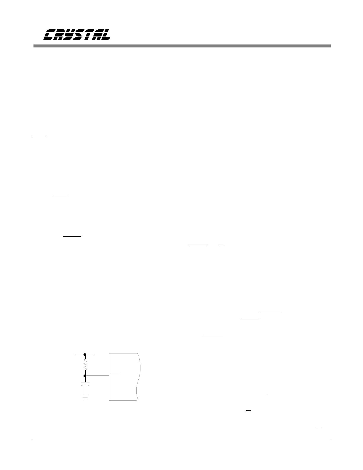
A simple power-on reset circuit can be built using a resistor and capacitor as shown in Figure 1. The RC time constant must be long
enough to guarantee the rest of the system is
fully powered up and stable by the end of reset.
+5V
R
C
Figure 1. Power-On Reset Circuit
CS5126
RST
Master Clock
The CS5126 operates from an externally-supplied master clock. In stereo operation, the master clock frequency is set at 512 times the perchannel sampling rate (256 in 2X oversampling
schemes). The CS5126 can accept master clocks
up to 24.576 MHz for 48kHz stereo sampling or
96kHz monaural oversampling.
All timing and control inputs for channel selection, sampling, and serial data transmission may
be divided down from the master clock. This
yields a completely synchronous system, avoiding sampling and conversion errors due to asynchronous digital noise.
CIRCUIT CONNECTIONS
Stereo Operation
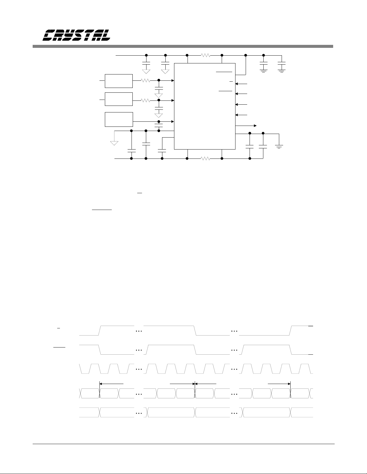
Figure 2 shows the standard circuit connections
for operating the CS5126 in its stereo mode. The
HOLD, L/R, and SCLK inputs are derived from
the master clock using a binary divider string. A
24.576 MHz master clock is required for a sampling rate of 48kHz per channel.
For 48kHz stereo sampling, the CS5126 must
sample and convert at a 96kHz rate to handle
both channels. The master clock is divided by
256 and applied to the HOLD input. A falling
transition on the HOLD pin places the input in
the hold mode and initiates a conversion cycle.
The HOLD input is latched internally by the
master clock, so it can return high anytime after
one master clock cycle plus 50ns.
In stereo operation the CS5126 alternately samples and converts the left and right input channels. This alternating channel selection is
achieved by dividing the HOLD input by two
(that is, dividing the master clock by 512) and
applying it to the L/R input. Upon completion of
each conversion cycle, the CS5126 automatically
returns to the track mode. The status of L/R as
6 DS32F1
CS5126
Left Ch.
Analog In
Right Ch.
Analog In
+5V
Anti Alias
Filter
Anti Alias
Filter
Voltage
Reference
-5V
1 µF
+
+
200
1 nF
200
1 nF
1
Ω
Ω
0.1
µ
F
0.1µF
µ
F
0.1
Figure 2. Stereo Mode Connection Diagram
each conversion finishes determines which channel is acquired and tracked. The L/R input must
remain valid at least until 30ns before the next
falling transition on HOLD.
As shown in the timing diagram in Figure 3, the
CS5126 uses pipelined data transmission. That
is, data from a particular conversion transmits
during the next conversion cycle. The serial
clock input, SCLK, is derived by dividing the
master clock by 16. The MSB (most-significantbit) will be stable on the first rising edge of
SCLK after a falling transition on HOLD. With
a serial clock of f
/16, transmission of all 16
clk
output bits will span an entire conversion and
acquisition cycle.
VA+
AINL
AINR
VREF
AGND
REFBUF
VA-
µ
F
10
CS5126
10
Ω
Ω
VD+
SLEEP
L/R
HOLD
SCLK
CLKIN
SDATA
DGND
VD-
0.1
0.1
f /512
clk
f /256
clk
f /16
clk
f
clk
F
µ
µ
F
1 µF
+
+
1 µF
STEREO MODE PERFORMANCE
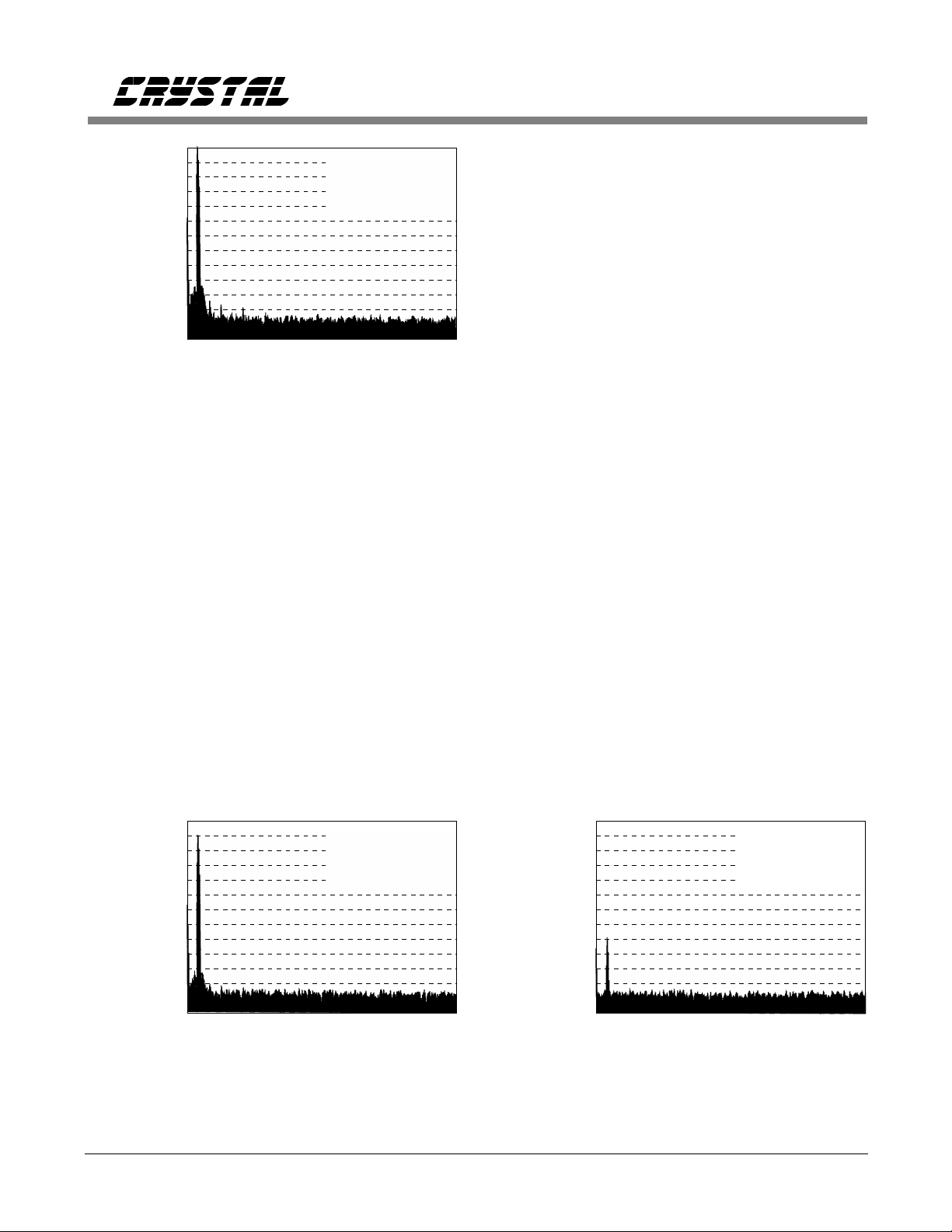
As illustrated in Figure 4, the CS5126 typically
provides 92dB S/(N+D) and 0.001% THD. Unlike conventional successive-approximation
ADC’s, the CS5126’s signal-to-noise and dynamic range are not limited by differential nonlinearities (DNL) caused by calibration errors.
Rather, the dominant noise source is broadband
thermal noise which aliases into the baseband.
This white broadband noise also appears as an
idle channel noise of 1/2 LSB (rms).
L/R (i)
HOLD (i)
SCLK (i)
Right Channel DataLeft Channel Data
SDATA (o)
Internal
Status
LSB MSB LSB MSB LSB MSB
Rch Conv. Lch Conv. Rch Acq.Lch Acq.
Figure 3. Stereo Mode Timing
DS32F1 7
CS5126
Signal
Amplitude
Relative to
Full Scale
0dB
-20dB
-40dB
-60dB
-80dB
-100dB
-120dB
1 kHz
Input Frequency
Sampling Rate: 48 kHz
Full Scale: 9V p-p
S/(N+D): 91.75 dB
S/(N+D): 92.53 dB
(dc to 20 kHz)
24kHz
Figure 4. FFT Plot of CS5126 in Stereo Mode
(Left Channel with 1 kHz, Full-Scale Input)
Differential Nonlinearity
The self-calibration scheme utilized in the
CS5126 features a calibration resolution of 1/4
LSB, or 18-bits. This ideally yields DNL of
±1/4 LSB, with code widths ranging from 3/4 to
5/4 LSB’s. This insures consistent sound quality
independent of signal level.
Traditional laser trimmed ADC’s have significant differential nonlinearities which are disastrous to sound quality with low-level signals.
Appearing as wide and narrow codes, DNL
often causes entire sections of the transfer func-
tion to be missing. Although their affect is minor
on S/(N+D) with high amplitude signals, DNL
errors dominate performance with low-level signals. For instance, a signal 80dB below fullscale will slew past only 6 or 7 codes. Half of
those codes could be missing with a conventional hybrid ADC capable of only 14-bit DNL.
The most common source of DNL errors in conventional ADC’s is bit weight errors. These can
arise due to accuracy limitations in factory trim
stations, thermal or physical stresses after calibration, and/or drifts due to aging or temperature
variations in the field. Bit-weight errors have a
drastic effect on a converter’s ac performance.
They can be analyzed as step functions superimposed on the input signal. Since bits (and their
errors) switch in and out throughout the transfer
curve, their effect is signal dependent. That is,
harmonic and intermodulation distortion, as well
as noise, can vary with different input conditions.
Differential nonlinearities in successive-approximation ADC’s also arise due to dynamic errors
in the comparator. Such errors can dominate if
the converter’s throughput/sampling rate is
driven too high. The comparator will not be allowed sufficient time to settle during each bit
decision in the successive-approximation algo-
Signal
Amplitude
Relative to
Full Scale
0dB
-20dB
-40dB
-60dB
-80dB
-100dB
-120dB
1 kHz
Input Frequency
Sampling Rate: 48 kHz
Full Scale: 9V p-p
S/(N+D): 83.27 dB
S/(N+D): 84.06 dB
(dc to 20 kHz)
a. Left Channel with 1 kHz, -10 dB Input
24kHz
Signal
Amplitude
Relative to
Full Scale
0dB
-20dB
-40dB
-60dB
-80dB
-100dB
-120dB
1 kHz
Input Frequency
Sampling Rate: 48 kHz
Full Scale: 9V p-p
S/(N+D): 13.70 dB
S/(N+D): 14.49 dB
(dc to 20 kHz)
b. Left Channel with 1 kHz, -80 dB Input
24kHz
Figure 5. FFT Plots of CS5126 in Stereo Mode
8 DS32F1
CS5126
rithm. The worst-case codes for dynamic errors
are the major transitions (1/2 FS; 1/4, 3/4 FS;
etc.). Since DNL effects are most critical with
low-level signals, the codes around in mid-scale,
(that is, 1/2 FS), are most important. Yet those
codes are worst-case for dynamic DNL errors!
With all linearity calibration performed on-chip
to 18-bits, the CS5126 maintains accurate bit
weights. DNL errors are dominated by residual
calibration errors of ±1/4 LSB rather than dynamic errors in the comparator. Furthermore, all
DNL effects on S/(N+D) are buried by white
broadband noise. This yields excellent sound
quality independent of signal level.
(See Figure 5)
Sampling Distortion
Like most discrete sample/hold amplifier de-
signs, the CS5126’s inherent sample/hold exhibits a frequency-dependent distortion due to
nonideal sampling of the analog input voltage.
The calibrated capacitor array used during conversions is also used to track and hold the analog input signal. The conversion is not performed on the analog input voltage per se, but is
actually performed on the charge trapped on the
capacitor array at the moment the HOLD command is given. The charge on the array ideally
assumes a linear relationship to the analog input
voltage. Any deviation from this linear relationship will result in conversion errors even if the
conversion process proceeds flawlessly.
At dc, the DAC capacitor array’s voltage coefficient dictates the converter’s linearity. This variation in capacitance with respect to applied signal voltage yields a nonlinear relationship between the charge on the array and the analog input voltage and places a bow or wave in the
transfer function. This is the dominant source of
distortion at low input frequencies (Figure 4).
0.020
0.016
0.012
THD (%)
0.008
0.004
0
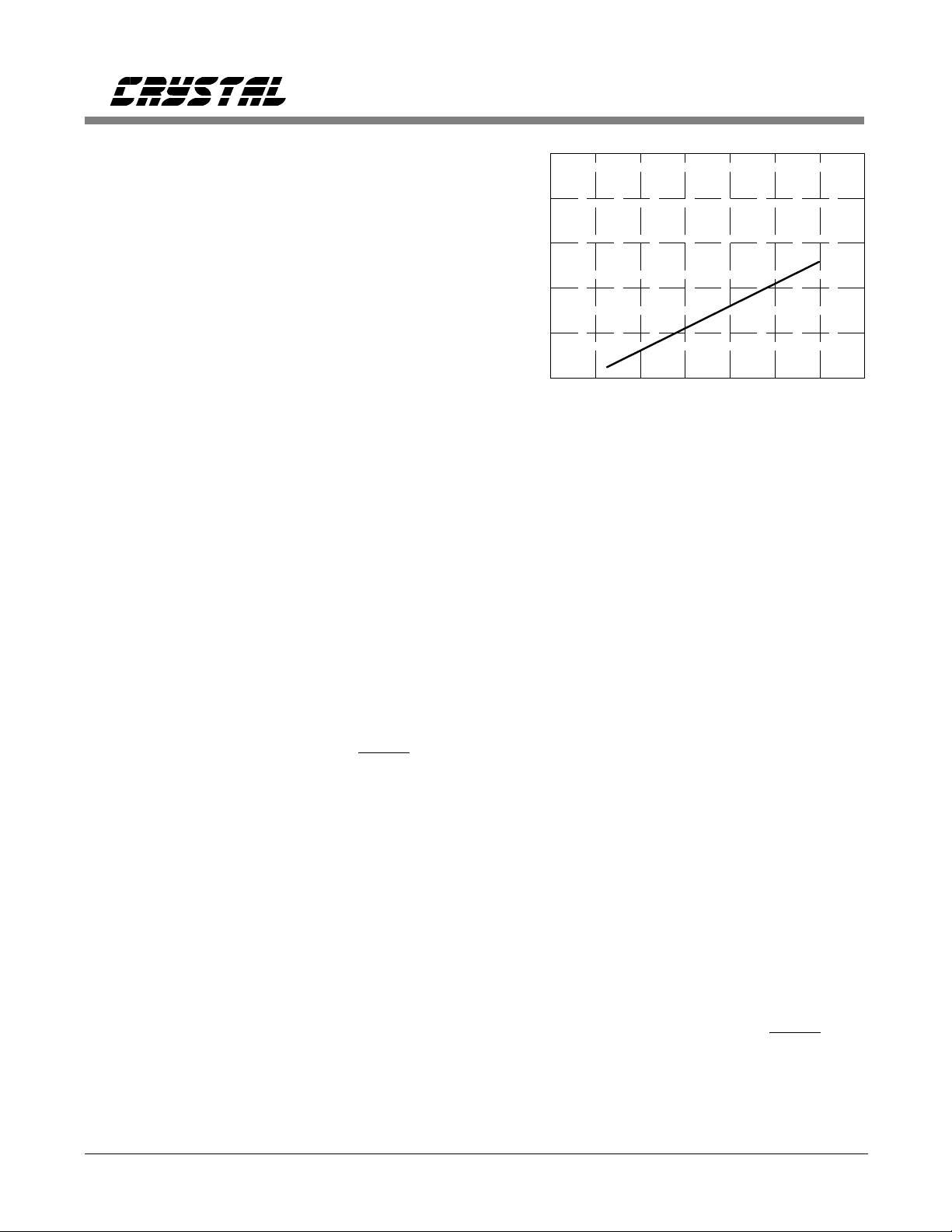
Figure 6. THD vs Input Frequency
5kHz 10kHz 15kHz 20kHz 25kHz
Analog Input Frequency
( 9V p-p Full-Scale Input)
The ideal relationship between the charge on the
array and the input voltage can also be distorted
at high signal frequencies due to nonlinearities
in the internal MOS switches. Dynamic signals
cause ac current to flow through the switches
connecting the capacitor array to the analog input pin in the track mode. Nonlinear on-resistance in the switches causes a nonlinear voltage
drop. This effect worsens with increased signal
frequency and slew rate as shown in Figure 6
since the magnitude of the steady state current
increases. First noticeable at 1kHz, this distortion assumes a linear relationship with input frequency. With signals 20dB or more below full-
scale, it no longer dominates the converter’s
overall S/(N+D) performance.
This distortion is strictly an ac sampling phenomenon. If significant energy exists at high frequencies, the effect can be eliminated using an
external track-and-hold amplifier to allow the ar-
ray’s charge current to decay, thereby eliminating any voltage drop across the switches. Since
the CS5126 has a second sampling function onchip, the external track-and-hold can return to
the track mode once the converter’s HOLD input
falls. It need only acquire the analog input by
the time the entire conversion cycle finishes.
DS32F1 9
CS5126
Simultaneous Sampling
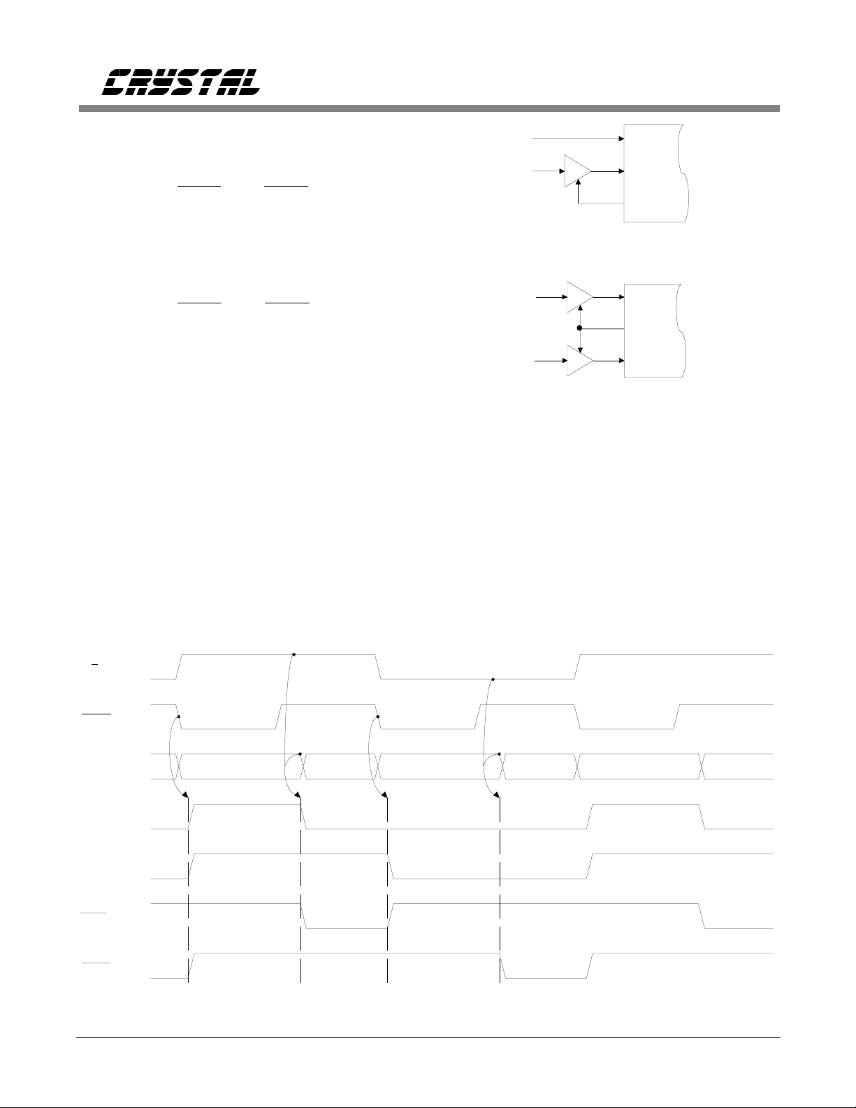
The CS5126 offers four digital output signals,
SSH1, SSH2, TRKL, and TRKR which can be
used to control external sample/hold amplifiers
to achieve simultaneous sampling and/or reduce
sampling distortion.
Figure 7 shows the timing relationships for
SSH1, SSH2, TRKL, and TRKR. In the stereo
configuration shown in Figure 1 the CS5126
samples the left and right channels 180° out of
phase. Simultaneous sampling between the left
and right channels can be achieved as shown in
Figure 8a using the CS5126’s SSH2 output. The
external sample/hold will freeze the right channel analog signal as the CS5126 freezes the left
channel input at AINL. It will hold that signal
valid at AINR until the CS5126 begins a right
channel conversion. Once that conversion begins, the sample/hold returns to the sample
mode. The acquisition time for the external sample/hold amplifier must not exceed the CS5126’s
minimum conversion time of 192 master clock
cycles (7.8µs for 48kHz stereo sampling).
AINL
S/H
AINR
SSH2
a. Standard Connections
S/H
AINL
SSH1
S/H
AINR
b. High-Slew Conditions
Figure 8. Simultaneous Sampling Connections
The CS5126’s sampling distortion with high-frequency, high-amplitude input signals may be improved if a low distortion sample/hold amplifier
is used as shown in Figure 8a. The right channel
input at AINR will appear as dc to the CS5126
resulting in no ac current flowing through the
internal MOS switches. Sampling distortion can
likewise be improved for both channels using
the SSH1 output as shown in Figure 8b. Simi-
L/R (i)
HOLD (i)
Internal
Status
SSH1 (o)
SSH2 (o)
TRKL (o)
TRKR (o)
10 DS32F1
Acq. & Track Hold
Acquire & Trac k Hold
Figure 7. External Sampling Control Output Timing
Lch Acq. Rch Acq. Rch Convert Lch Acq.Lch ConvertRch Convert
 Loading...