

Page 1

K
CS5521
CS5523
2- or 4-Channel 16-Bit Buffered
Features
l Delta-Sigma A/D Converter
— Linearity Error: 0.0015%FS
l Buffered Bipolar/Unipolar Input Ranges
— 25 mV, 55 mV, 100 mV, 1 V, 2.5 V and 5 V
l Chopper Stabilized Instrumentation Amplifier
l On-Chip Charge Pump Drive Circuitry
l Differential Multiplexer
l Conversion Data FIFO
l Programmable/Auto Channel Sequencer
l 2-Bit Output Latch
l Simple three-wire serial interface
— SPI™ and Microwire™ Compatible
— Schmitt Trigger on Serial Clock (SCLK)
l Output Settles in One Conversion Cycle
l 50/60 Hz ±3 Hz Simultaneous Rejection
l Buffered V
l System and Self-Calibration with R/W
Registers per Chan nel
l Single +5 V Analog Supply
+3.0 V or +5 V Digital Supply
l Power Consumption: 5.5 mW
- 1.8 mW in 1 V, 2.5 V and 5 V input ranges
with +5 V Input Capability
REF
∆Σ
Multi-Range ADC
General Description
The 16-bit CS5521/23 are highly integrated ∆Σ A/D converters which include an instrumentation amplifier, a PGA
(programmable gain amplifie r), a multi-channel multiplexe r,
digital filters, and sel f and syst em cali bration circu itry.
The chips are designed to provide their own negative
supply which enables their on-chi p instrumentati on amplifiers to measure bipolar ground-referenced signals
less-than or equal to ±100 mV.
The digital filters p rovide programmable output update
rates of 1.88 Hz, 3.76 Hz, 7.51 Hz, 15 Hz, 30 Hz,
61.6 Hz, 84.5 Hz, and 101.1 Hz when operating from a
32 kHz crystal. The CS5521/23 are capable of producing
output update rates up t o 303 Hz with a 100kHz clock .
The filters are desi gned to s ettle to fu ll accurac y for the
selected output update rate within one conversion cycle.
When operated at word rates of 15 Hz or less, the digital
filters reject both 50 and 60 Hz line interference
simultaneously.
Low power, single conversion settling time, programmable output rates, and the ability to handle ne gative inpu t
signals make these single supply products ideal solutions for isolated and non-isolated applications.
ORDERING INFORMATION
See page 33.
±3Hz
VA+
+
X20
-
Latch
A0 A1
X1
X1
AIN1+
AIN1AIN2+
AIN2-
AIN3+
AIN3AIN4+
AIN4-
NBV
MUX
CS5523
Shown
CPD
Preliminary Product Information
Cirrus Logic, Inc.
Crystal Semiconductor Products Division
P.O. Box 17847, Austin, Texas 78760
(512) 445 7222 FAX: (512) 445 7581
http://www.crystal.com
AGND
Programmable
Gain
Calibration
Memory
This document contains information for a new product.
Cirrus Logic reserves the right to modify this product without notice.
VREF+
VREF-
X1
Differential
4th order
delta-sigma
modulator
Calibra tion
Copyright Cirrus Logic, Inc. 1999
(All Rights Reserved)
µ
C
Digital Filter
Clock
Gen.
XIN XOUT
VD+DGND
Calibra tion
Register
Control
Register
Output
Register
CS
SCL
SDI
SDO
MAR ‘99
DS317PP2
1
Page 2

TABLE OF CONTENTS
CHARACTERISTICS/SPECIFICATIONS ................................................ ............4
ANALOG CHARACTERISTICS................................................................... 4
RMS NOISE.................................................................................................4
5 V DIGITAL CHARACTERISTICS ............................................................. 6
3 V DIGITAL CHARACTERISTICS ............................................................. 6
DYNAMIC CHARACTERISTICS ................................................................. 7
RECOMMENDED OPERATING CONDITIONS.......................................... 7
ABSOLUTE MAXIMUM RATINGS.............................................................. 7
SWITCHING CHARACTERISTICS .................................... ....... ...... ....... ..... 8
GENERAL DESCRIPTION ................................................................................ 10
Theory of Operation .................................................................................. 10
System Initialization ........................... ....... ...... ...... ....... ...... .......................12
Serial Port Overview ................................................................................. 12
Serial Port Interface .................................................................................. 13
Serial Port Initialization ............................................................................. 13
Channel-Setup Registers ...... ....... ...... ....... ...... ....................................... ... 13
Conversion Protocol ................................................................................. 13
Calibration Protocol ..................................................................................19
Use of Pointers in Command Byte ............................................................20
Analog Input ............................................................................................. 21
Charge Pump Drive ..................................................................................23
Voltage Reference .................................................................................... 24
Calibration .................................................................................................24
Self Calibration .........................................................................................25
System Calibration ................ ....... ...... ....... ...... ...... ....... ............................. 25
Calibration Tips ......................................................................................... 27
Limitations in Calibration Range ............................................................... 27
Analog Output Latch Pins ......................................................................... 28
Output Word Rate Selection ..................................................................... 28
Clock Generator ........................................................................................28
Digital Filter ...............................................................................................28
Output Coding .......................................................................................... 28
Power Consumption .................................................................................29
PCB Layout .............................................................................................. 30
PIN DESCRIPTIONS ......................................................................................... 31
Clock Generator ........................................................................................31
Control Pins and Serial Data I/O ...............................................................31
Measurement and Reference Inputs ........................................................32
Power Supply Connections .......................................................................32
SPECIFICATION DEFINITIONS ........................................................................ 33
ORDERING GUIDE ............................................................................................ 33
PACKAGE DESCRIPTIONS ............................................................................. 34
CS5521 CS5523
SPI™ is a trademark of Motorola Inc., Microwire™ is a trademark of National Semiconductor Corp.
Prelimina ry pro du ct i nfo rma tion desc ri bes prod ucts wh ich are i n pr oduc ti on, bu t f or w hich ful l c har act eri za tion d ata is not yet available. Advance
product information describes products which are in development and subject to development changes. Cirrus Logic, Inc. has made best efforts
to ensure that the information contained in this document is accurate and reliable. However, the information is subject to change without notice
and is provided “AS IS” without warranty of any kind (express or implied). No responsibility is assumed by Cirrus Logic, Inc. for the use of this
information, nor for infringements of patents or other rights of third parties. This document is the property of Cirrus Logic, Inc. and implies no
license unde r patents, copyri g ht s , trademarks, or t r ade secrets. No p art of this publication may be copied, reproduc e d , s tored in a retrieval system, or transmitted, in any form or by any means (electronic, mechanical, photographic, or otherwise). Furthermore, no part of this publicat ion
may be used as a basis for manufacture or sale of any items without the prior written consent of Cirrus Logic, Inc. The names of products of
Cirrus Logic, Inc. or other vendors and suppliers appearing in this document may be trademarks or service marks of their respective owners
which may be registered in some jurisdictions. A list of Cirrus Logic, Inc. trademarks and service marks can be found at http://www.cirrus.com.
2 DS317PP2
Page 3

TABLE OF FIGURES
CS5521/23 Configured to use on-chip charge pump to supply NBV. ................ 10
Charge Pump Drive Circuit for VD+ = 3 V. ......................................................... 11
Alternate NBV Circuits. ...................................................................................... 11
CS5521/23 Configured for ground-referenced Unipolar Signals. ....................... 11
CS5521/23 Configured for Single Supply Bridge Measurement. ....................... 12
Command and Data Word Timing. ..................................................................... 15
Multiplexer Configuration ................................... ...... ...... ....... ...... ....... ...... ....... ... 22
Input models for AIN+ and AIN- pins for each range. ........................................ 24
Input model for VREF+ and VREF- pins. ........................................................... 24
Self Calibration of Offset (Low Ranges). ............................................................ 26
Self Calibration of Offset (High Ranges). ........................................................... 26
Self Calibration of Gain (All Ranges). ................................................................ 26
System Calibration of Offset (Low Ranges). ...................................................... 26
System Calibration of Offset (High Ranges). ..................................................... 26
System Calibration of Gain (Low Ranges) ......................................................... 26
System Calibration of Gain (High Ranges). ....................................................... 26
Filter Response (Normalized to Output Word Rate = 1) .................................... 28
CS5521 CS5523
DS317PP2 3
Page 4

CHARACTERISTICS/SPECIFICATIONS
CS5521 CS5523
ANALOG CHARACTERISTICS (T
NBV = -2.1 V, FCLK =32.768 kHz, OWR (Output Word Rate) = 15.0 Hz, Bipolar Mode, Input Range = ±100 mV;
See Notes 1 and 2.)
Parameter Min Typ Max Unit
= 25 °C; VA+, VD+ = 5 V ±5%; VREF+ = 2.5 V, VREF- = AGND,
A
Accuracy
Resolution - - 16 Bits
Linearity Error Bipolar Offset (Note 3) Unipolar Offset (Note 3) Offset Drift (Notes 3 and 4) - 20 - nV/°C
Bipolar Gain Error Unipolar Gain Error Gain Drift (Note 4) - 1 3 ppm/°C
±
0.0015±0.003 %FS
±
1±2LSB
±
2
±
8
±
16
±
4LSB
±
31 ppm
±
62 ppm
Voltage Reference Input
Range (VREF+) - (VREF-) 1 2.5 VA+ V
VREF+
VREF- NBV Common Mode Rejection dc
50, 60 Hz
Input Capacitance - 16 - pF
CVF Current (Note 5) - 5.0 - nA
(VREF-)+1
-
-
-VA+V
110
130
(VREF+)-1
-
-
V
dB
dB
16
16
Notes: 1. Applies after system calibration at any temperature within -40 °C ~ +85 °C.
2. Specifications guaranteed by design, characterization, and/or test.
3.
Specification applies to the device only and does not include any effects by external parasitic thermocouples.
4. Drift over specified temperature range after calibration at power-up at 25 °C.
5. See the section of the data sheet which discusses input models.
RMS NOISE (Notes 6 and 7)
Output Rate
(Hz)
1.88 1.64 90 nV 148 nV 220 nV 1.8 µV 3.9 µV 7.8 µV
3.76 3.27 122 nV 182 nV 310 nV 2.6 µV 5.7 µV 11.3 µV
7.51 6.55 180 nV 267 nV 435 nV 3.7 µV 8.5 µV 18.1 µV
15.0 12.7 280 nV 440 nV 810 nV 5.7 µV 14 µV 28 µV
30.0 25.4 580 nV 1.1 µV 2.1 µV 18.2 µV 48 µV 96 µV
61.6 50.4 2.6 µV 4.9 µV 8.5 µV 92 µV 238 µV 390 µV
84.5 (Note 8) 70.7 11 µV 27 µV 43 µV 458 µV 1.1 mV 2.4 mV
101.1 (Note 8) 84.6 41 µV 72 µV 130 µV 1.2 mV 3.4 mV 6.7 mV
Notes: 6. Wideband noise aliased into the baseband. Referred to the input. Typical values shown for 25 °C.
7. For Peak-to-Peak Noise multiply by 6.6 for all ranges and output rates.
8. For input ranges <100 mV and output rates >61.6 Hz 16.384 kHz chopping frequency is used.
-3 dB Filter
Frequency
25 mV 55 mV 100 mV 1 V 2.5 V 5 V
Input Range, (Bipolar/Unipolar Mode)
4 DS317PP2
Page 5

CS5521 CS5523
ANALOG CHARACTERISTICS (Continued)
Parameter Min Typ Max Unit
Analog Input
Common Mode + Signal on AIN+ or AIN- Bipolar/Unipolar Mode
NBV = -1.8 to -2.5 V Range = 25 mV, 55 mV, or 100 mV
Range = 1 V , 2.5 V, or 5 V
NBV = AGND Range = 25 mV, 55 mV, or 100 mV
Range = 1 V , 2.5 V, or 5 V
Common Mode Rejection dc
50, 60 Hz
-0.150
NBV
1.85
0.0
-
-
-
-
-
-
120
120
Input Capacitance - 10 - pF
CVF Current on AIN+ or AIN- (Note 5)
Range = 25 mV, 55 mV, or 100 mV
Range = 1 V , 2.5 V, or 5 V
-
-
100
10
System Calibration Specifications
Full Scale Calibration Range Bipolar/Unipolar Mode
25 mV
55 mV
100 mV
1 V
2.5 V
5 V
10
25
40
0.40
1.0
2.0
-
-
-
-
-
-
Offset Calibration Range Bipolar/Unipolar Mode
25 mV
55 mV
100 mV (Note 9)
1 V
2.5 V
5 V
-
-
-
-
-
-
-
-
-
-
-
-
Power Supplies
DC Power Supply Currents (Normal Mode) I
(Note 10) I
I
NBV
A+
D+
Power Consumption Normal Mode (Note 11)
Standby
Sleep
Power Supply Rejection dc Positive Supplies
dc NBV
-
-
-
-
-
-
-
-
0.9
90
260
5.5
1.2
500
120
110
0.950
VA+
2.65
VA+
-
-
300
-
32.5
71.5
105
mV
mV
mV
1.30
3.25
VA+
±12.5
±27.5
±50
mV
mV
mV
±0.5
±1.25
±2.50
1.2
mA
135
375
7.5
-
-
mW
mW
µW
-
-
V
V
V
V
dB
dB
pA
nA
V
V
V
V
V
V
µA
µA
dB
dB
Notes: 9. The maximum full scale signal can be limited by saturation of circuitry within the internal signal path.
10. Measured with Charge Pump Drive off.
11. All outputs unloaded. All input CMOS levels.
DS317PP2 5
Page 6

CS5521 CS5523
5 V DIGITAL CHARACTERISTICS (T
= 25 °C; VA+, VD+ = 5 V ±5%; GND = 0;
A
See Notes 2 and 12.)
Parameter Symbol Min Typ Max Unit
High-Level Input Voltage All Pins Except XIN and SCL K
XIN
SCLK
Low-Level Input Voltage All Pins Except XIN and SCLK
XIN
SCLK
High-Level Output Voltage
All Pins Except CPD and SDO (Note 13)
CPD, I
SDO, I
= -4.0 mA
out
= -5.0 mA
out
Low-Level Output Voltage
All Pins Except CPD and SDO, I
CPD, I
SDO, I
= 1.6 mA
out
= 2 mA
out
= 5.0 mA
out
Input Leakage Current I
3-State Leakage Current I
Digital Output Pin Capacitance C
Notes: 12. All measurements performed under static conditions.
13. I
= -100 µA unless stated otherwise. (VOH = 2.4 V @ I
out
V
IH
V
IL
V
OH
V
OL
in
OZ
out
out
0.6 VD+
(VD+)-0.5
(VD+) - 0.45
(VA+) - 1.0
(VD+) - 1.0
(VD+) - 1.0
= -40 µA.)
-
-
-
-
-
-
-
-
-
-
-
-
-
-
-
-
-
-
-
-
-
0.8
1.5
0.6
-
-
-
0.4
0.4
0.4
V
V
V
V
V
V
V
V
V
V
V
V
-±1±10µA
--±10µA
-9-pF
3 V DIGITAL CHARACTERISTICS (T
= 25 °C; VA+ = 5 V ±5%; VD+ = 3.0 V ±10%; GND = 0;
A
See Notes 2 and 12.)
Parameter Symbol Min Typ Max Unit
High-Level Input Voltage All Pins Except XIN and SCL K
XIN
SCLK
Low-Level Input Voltage All Pins Except XIN and SCLK
XIN
SCLK
High-Level Output Voltage
All Pins Except CPD and SDO, I
CPD, I
SDO, I
= -400 µA
out
= -4.0 mA
out
= -5.0 mA
out
Low-Level Output Voltage
All Pins Except CPD and SDO, I
CPD, I
SDO, I
= 400 µA
out
= 2 mA
out
= 5.0 mA
out
Input Leakage Current I
3-State Leakage Current I
Digital Output Pin Capacitance C
V
IH
V
IL
V
OH
V
OL
in
OZ
out
0.6 VD+
(VD+)-0.5
(VD+) - 0.45
-
-
-
(VA+) - 0.3
(VD+) - 1.0
(VD+) - 1.0
-
-
-
-
-
-
-
-
-
-
-
-
-
-
-
-
-
-
0.16 VD+
0.3
0.6
-
-
-
0.3
0.4
0.4
-±1±10µA
--±10µA
-9-pF
V
V
V
V
V
V
V
V
V
V
V
V
6 DS317PP2
Page 7

DYNAMIC CHARACTERISTICS
Parameter Symbol Ratio Unit
Modulator Sampling Frequency f
Filter Settling Time to 1/2 LSB (Full Scale Step) t
CS5521 CS5523
s
s
XIN/4 Hz
1/f
out
s
RECOMMENDED OPERATING CONDITIONS
(AGND, DGND = 0 V; See Note 14.)
Parameter Symbol Min Typ Max Unit
DC Power Supplies Positive Digital
Positive Analog
Analog Reference Voltage (VREF+) - (VREF-) VRef
VD+
VA+
diff
2.7
4.75
5.0
5.0
5.25
5.25
1.0 2.5 VA+ V
V
V
Negative Bias Voltage NBV -1.8 -2.1 -2.5 V
Notes: 14. All voltages with respect to ground.
ABSOLUTE MAXIMUM RATINGS (AGND, DGND = 0 V; See Note 14.)
Parameter Symbol Min Typ Max Unit
DC Power Supplies (Note 15)
Positive Digital
Positive Analog
Negative Bias Voltage Negative Potential NBV +0.3 -2.1 -3.0 V
Input Current, Any Pin Except Supplies (Note 16 and 17) I
Output Current I
Power Dissipation (Note 18) PDN - - 500 mW
Analog Input Voltage VREF pins
AIN Pins
Digital Input Voltage V
Ambient Operating Temperature T
Storage Temperature T
VD+
VA+
IN
OUT
V
INR
V
INA
IND
stg
-0.3
-0.3
-
-
+6.0
+6.0
V
V
--±10mA
--±25mA
NBV -0.3
NBV -0.3
--(VA+) + 0.3
(VA+) + 0.3VV
-0.3 - (VD+) + 0.3 V
A
-40 - 85 °C
-65 - 150 °C
Notes: 15. No pin should go more negative than NBV - 0.3 V.
16. Applies to all pins including continuous overvoltage conditions at the analog input (AIN) pins.
17. Transient current of up to 100 mA will not cause SCR latch-up. Maximum input current for a power
supply pin is ±50 mA.
18. Total power dissipation, including all input currents and output currents.
WARNING: Operation at or beyond these limits may result in permanent damage to the device.
Normal operation is not guaranteed at these extremes.
DS317PP2 7
Page 8

CS5521 CS5523
SWITCHING CHARACTERISTICS (T
Levels: Logic 0 = 0 V, Logic 1 = VD+; C
= 50 pF.)
L
= 25 °C; VA+ = 5 V ±5%; VD+ = 3.0 V ±10% or 5 V ±5%;
A
Parameter Symbol Min Typ Max Unit
Master Clock Frequency (Note 19)
External Clock or Internal Oscillator
XIN
30 32.768 100 kHz
Master Clock Duty Cycle 40 - 60 %
Rise Times (Note 20)
Any Digital Input Except SCLK
SCLK
Any Digital Output
Fall Times (Note 20)
Any Digital Input Except SCLK
SCLK
Any Digital Output
t
rise
t
fall
-
-
-
-
-
-
50
50
-
-
-
-
1.0
100
-
1.0
100
-
µs
µs
ns
µs
µs
ns
Start-up
Oscillator Start-up Time XTAL = 32.768 kHz (Note 21) t
Power-on Reset Period t
ost
por
-500-ms
- 2006 - XIN
cycles
Serial Port Timing
Serial Clock Frequency SCLK 0 - 2 MHz
SCLK Falling to CS
Falling for continuous running SCLK
t
0
100 - - ns
(Note 22)
Serial Clock Pulse Width High
Pulse Width Low
t
1
t
2
250
250
-
-
-
-
ns
ns
SDI Write Timing
CS Enable to Valid Latch Clock t
Data Set-up Time prior to SCLK rising t
Data Hold Time After SCLK Rising t
SCLK Falling Prior to CS
Disable t
3
4
5
6
50 - - ns
50 - - ns
100 - - ns
100 - - ns
SDO Read Timing
CS to Data Valid t
SCLK Falling to New Data Bit t
Rising to SDO Hi-Z t
CS
7
8
9
--150ns
--150ns
--150ns
Notes: 19. Device parameters are specified with a 32.768 kHz clock; however, clocks up to 100 kHz can be used
for increased throughput.
20. Specified using 10% and 90% points on waveform of interest. Output loaded with 50 pF.
21. Oscillator start-up time varies with crystal parameters. This specification does not apply when using an
external clock source.
22. Applicable when SCLK is continuously running.
Specifications are subject to change without notice.
8 DS317PP2
Page 9

CS
CS
SCLK
CS5521 CS5523
t
0
t
t
t
3
1
t
2
Continuous Running SCLK Timing (Not to Scale)
t
3
6
CS
SDO
SCLK
SCLK
t
7
MSB
MSB
MSB-1 LSBSDI
t
4
t
5
t
1
t
2
t
6
SDI Write Timing (Not to Scale)
t
9
MSB-1 LSB
t
8
t
2
t
1
SDO Read Timing (Not to Scale)
DS317PP2 9
Page 10

CS5521 CS5523
GENERAL DESCRIPTION
The CS5521/23 are 16-bit converters which include a chopper-stabilized instrumentation amplifier, and an on-chip programmable gain amplifier.
They are optimized for measuring low-level unipolar or bipolar signals in process control and medical
applications.
The CS5521/23 also include a fourth order deltasigma modulator, a calibration microcontroller,
eight digital filters used to select between eight output update rates, a 2-bit analog latch, a multiplexer,
and a serial port.
The CS5521/23 include a CPD (Charge Pump
Drive) output (shown in Figure 1) which provides
a negative bias voltage to the on-chip instrumentation amplifier when used with a combination of external diodes and capacitors. This makes the
converters ideal for thermocouple temperature
measurements because the biasing scheme enables
the CS5521/23 to measure negative voltages with
respect to ground without the need for a negative
supply.
Theory of Operation
The CS5521/23 A/D converters are designed to operate from a single +5 V analog supply with several
different input ranges. See the Analog Character-
istics section on page 3 for details.
Figure 1 illustrates the CS5521/23 connected to
generate their own negative bias supply using the
on-chip CPD (Charge Pump Drive). This e nables
the CS5521/23 to measure ground referenced signals with magnitudes down to -100mV. Figure 2 illustrates a charge pump circuit when the converters
are powered from a +3.0 V digital supply. Alternatively, the negative bias supply can be generated
from a negative supply voltage or a resistive divider as illustrated in Figure 3.
+5V
Analog
Supply
Cold Junction
LM334
Absolute
Current
Reference
2.5V
Up to ± 100 mV Input
Ω
10 k
BAV199
0.1 µF
10 k
Ω
+5V
V+
R
Ω
499
V-
301
Ω
10
Ω
0.1 µF0.1
20
19
3
4
1
18
17
16
6
BAT85
VA+
VREF+
VREF-
AIN1+
AIN1AGND
AIN2+
AIN2-
A1
A0
2
CS5521
5
1N4148
10 µF
+
CPD
14
VD+
XOUT
SCLK
SDO
DGNDNBV
7
0.03 µF
1N4148
XIN
CS
SDI
11
32.768 ~ 100 kHz
10
9
15
8
12
Logic Outputs:
A0 - A1 Switc h from
13
VA+ to AGND.
Charge-pump network
for VD+ = 5V only and
XIN = 32.768 kHz.
Optional
Interface
Clock
Source
Serial
Data
F
µ
Figure 1. CS5521/23 Configured to use on-chip charge pump to supply NBV.
10 DS317PP2
Page 11

CS5521 CS5523
S
0.1
µF
SerialDataInterface732.768 ~ 100 kH
z
Figure 4 illustrates the CS5521/23 connected to
measure ground referenced unipolar signals of a
positive polarity using the 1 V, 2.5 V, and 5 V ranges on the converter. For the 25 mV, 55 mV, and 100
mV ranges the signal must have a common mode
for the measurement of ratiometric bridge transducer outputs. Figure 5 illustrates the CS5521/23
connected to measure the output of a ratiometric
differential bridge transducer while operating from
a single +5 V supply.
near +2.5 V (NBV = 0V).
The CS5521/23 are optimized for the measurement
of thermocouple outputs, but are also well suited
2N5087
BAT85
or similar
10µF
+
NBV
Figure 2. Charge Pump Drive Circuit for VD+ = 3 V. Figure 3. Alternate NBV Circuits.
-5V
34.8K
30.1K
Ω
NBV
Ω
2.0K
BAT85
+
Ω
-5V
2.1K
10 µF
Ω
10
+5V
Analog
Supply
0 to +5V Input
CM = 0 to V A +
0.1
+
-
F
µ
20
VREF+
19
VREF-
3
AIN1+
4
AIN1-
1
AGND
18
AIN2+
17
AIN2-
16
A1
6
A0
Ω
214
VD+VA+
CS55 1
CPD
XOUT
SCLK
SDO
DGNDNBV
135
XIN
C
SDI
11
10
9
15
8
12
Optional
Clock
Source
Figure 4. CS5521/23 Configured for ground-referenced Unipolar Signals.
DS317PP2 11
Page 12

SCLKSDOSD
I
C
S
10
0.1
µF
l
SerialDataInterface732.768 ~ 100kHz
configuration registe r: 000040(H)
offset registers: 000000(H)
gain registers: 400000(H)
channel setup regist ers: 000000(H)
+5V
Analog
Supply
-
Figure 5. CS5521/23 Configured for Single Supply Bridge Measurement.
+
0.1
F
µ
VA+
20
VREF+
19
VREF-
AIN1+
3
4
AIN1-
1
AGND
18
AIN2+
17
AIN2-
16
A1
6
A0
Ω
214
CS5521
CPD
VD+
XOUT
DGNDNBV
XIN
135
11
10
9
15
8
12
CS5521 CS5523
Optiona
Clock
Source
System Initialization
When power to the CS5521/23 are applied, the
chips are held in a reset condition until the 32.768
kHz oscillator has started and a counter-timer
elapses. Due to the high Q of the 32.768 kHz crystal, the oscillator takes 400-600 ms to start. The
counter-timer counts 2006 oscillator clock cycles
to make sure the oscillator is fully stable. During
this time-out period the serial port logic is re set and
the RV (Reset Valid) bit in the configuration register is set to indicate that a valid reset occurred. After a reset, the on-chip registers are initialized to the
following states and the converter is placed in the
command mode where it waits for a valid command.
Note: A system reset can be initiated at any time by writing a
logic 1 to the RS (Reset System) bit in the conf iguration register. After a reset, the RV bit is set until t he configuration
register is read. The user must then write a logic 0 to the RS
bit to take the part out of reset mode.
12 DS317PP2
Serial Port Overview
The CS5521/23’s serial port includes a microcontroller which contains a command register, a configuration register, and a gain and offset register for
each input channel. The serial port also includes a
programmable channel sequencer which can sequence up to 8 channels to be converted. The sequencer consists of channel-setup registers (CSRs)
which contain information about the modes used
when conversions are performed. To complement
the sequencer a conversion data FIFO (CDF, read
only) is included to store up to sixteen data conversions. All registers except the 8-bit command register are 24-bits in length. The conversion data
FIFO is just an array of 24-bit conversion data registers used to store conversion words until the FIFO
is read.
The serial port has two modes of operation: the
command mode and the data mode. After a system
initialization or reset, the serial port is initialized
into command mode where it waits to receiv e a valid command (the first 8-bits into the serial port).
Tables 1 and 2 can be used to decode all valid commands. Once a valid command is received, the byte
Page 13

CS5521 CS5523
instructs the converter to read from or write to a
register(s), perform a conversion or a calibration,
or perform a NULL command. If a command other
than start calibration or NULL command is received, the serial port enters data mode. In data
mode, either the internal registers, the CS Rs, or the
CDF (read only) are read from or written to. The
number of bytes transferred depends on the type of
register/FIFO being accessed and the way it is accessed. Once the data is transferred, the serial port
either remains in data mode or returns to the command mode. The mode which is entered depends
on the status of the loop (LP), the MC (multiple
conversion), and the RC (read convert) bits in the
configuration register. More information concerning the LP bit is provided in the Conversion/Calibration Protocol section. Note that SDO will fall to
logic 0 anytime a calibration or conversion is completed.
Serial Port Interface
The CS5521/23’s serial interface consists of four
control lines: CS, SCLK, SDI, SDO.
CS, Chip Select, is the control line which enables
access to the serial port. If the CS pin is tied low,
the port can function as a three wire interface.
SCLK, Serial Clock, is the serial bit-clock which
controls the shifting of data to or from the ADC’s
serial port. The CS pin must be held low (logic 0)
before SCLK transitions can be recognized by the
port logic.
SDI, Serial Data In, is the data signal used to transfer data to the converters.
SDO, Serial Data Out, is the data signal used to
transfer output data from the converters. The SDO
output will be held at high impedance any time CS
is at logic 1. Figure 6 illustrates the serial sequence
necessary to write to, or read from the serial port’s
registers.
To accommodate optoisolators SCLK is designed
with a Schmitt-trigger input to allow an optoisola-
tor with slower rise and fall times to directly drive
the pin. Additionally, SDO is capable of sinking or
sourcing up to 5 mA to directly drive an optoisolator LED. SDO will have less than a 400 mV loss in
the drive voltage when sinking or sourcing 5 mA.
Serial Port Initialization
The serial port is initialized to the command mode
whenever a power-on reset is performed inside the
converter, or when the user transmits the port initialization sequence. The port initialization sequence involves clocking 15 bytes of all 1's,
followed by one byte with the contents ‘11111110’.
This sequence places the chip into command mode
where it awaits a valid command.
Channel-Setup Registers
Table 3 depicts the channel-setup registers (CSRs).
The CS5521 has two CSRs and the CS5523 has four
CSRs. Each CSR contains two logical channels
which are programmed by the user to contain data
conversion information such as: 1) state of the output latch pins, 2) output word rate, 3) gain range, 4)
polarity, and 5) the address of a physical input channel to be converted. Note that any physical input
channel can be represented in more than one logical
channel with different output rates, gain ranges, and
conversion modes. Once programmed the CSRs act
as a sequencer and determine the order in which conversions are performed. To program the CSRs
twelve bits are needed for each logical channel. For
example, to configure CSR #2 in the CS5521, bits 23
to 12 contain information on the third logical channel and bits 11 to 0 contain information on the fourth
logical channel. While reading/writing CSRs, only
an even number of logical channels are accessed.
The depth bits in the configuration register can only
be: 001, 011, 101, 111 when accessing CSRs.
Conversion Protocol
To acquire single or multiple conversion(s) a command byte is issued with its MSB=1 and CC2-CC0
= ‘000’. The type of conversion(s) performed and
DS317PP2 13
Page 14

C
ommand Register
D7(MSB)D6D5D4D3D2D1D0
CB NU CSB1 CSB0 R/W RSB2 RSB1 RSB0
BIT NAME VALUE FUNCTION
D7 Command Bit, CB 0
1
D6 Not Used, NU 0 Must always be logic zero.
D5-D4 Channel Select Bits,
CSB1-CSB0
D3 Read/Write, R/W 0
D2-D0 Register Select Bit,
RSB2-RSB0
00
.
.
11
1
000
001
010
011
100
101
110
111
Must be logic 0 for these commands.
See Table 2.
CSB1-CSB0 provide the address of one of the four physical
channels. These bits are used to access the c al ibra tion registers associated with respective channels.
Note: These bits are ignored when reading the data register.
Write to selected register.
Read from selected register.
Reserved
Offset Register
Gain Register
Configuration Register
Conversion Data FIFO (read only)
Channel Set-up Registers
- register is 48-bits long for CS5521
- register is 96-bits long for CS5523
Reserved
Reserved
CS5521 CS5523
Table 1. Command-Set with MSB=0
D7(MSB)D6D5D4D3D2D1D0
CB NU CPB2 CPB1 CPB0 CC2 CC1 CC0
BIT NAME VALUE FUNCTION
D7 Command Bit, CB 0
1
D6 Not Used, NU 0 Must always be logic zero.
D5-D3 Channel Pointer Bits,
CPB2-CPB0
D2-D0 Conversion/Calibration
Bits, CC2-CC0
000
.
.
.
111
000
001
010
011
100
101
110
111
See Table 1.
Must be logic 1 for these commands.
These bits are used as pointers to the logical channels.
Note: The MC bit, must be logi c 0 for these bi t s to t ake e ff ect .
When MC = 1, these bits are ignored. The LP, MC, and RC
bits in the configuration register are ignored during calibration.
Normal Conversion
Self-Offset Calibration
Self-Gain Calibration
Reserved
Reserved
System-Offset Cali brati on
System-Gain Calibration
Reserved
Table 2. Command-Set with MSB=1
14 DS317PP2
Page 15

CS
SCLK
CS5521 CS5523
SDI
CS
SCLK
SDI
SDO
Command Time
8 SCLKs
Command Time
8 SCLKs
MSB
Write Cycle
MSB
Read Cycle
LSB
Data Tim e 24 SCLKs
LSB
Data Time 24 SCLK s
SCLK
SDI
t *
Command Time
d
8 SCLKs
SDO
8 SCLKs Cl ea r SD O Fla g
* td = XIN /OWR clock cycles for ea c h conversion except the
first conversion which will take XIN/OWR + 7 clock cycles
MSB
Data Time
24 SCLKs
XIN/OWR
Clock Cycles
LSB
Figure 6. Command and Data Word Ti ming.
DS317PP2 15
Page 16

CS5521 CS5523
Channel-Setup Registers
CSR (Channel-Setup Register) CSR
#1 LC (Log. Channel) 1
Bits <47:36>
#2 LC 3
Bits <23:12>
CS5521 CS5523
D23(MSB) D22 D21 D20 D19 D18 D17 D16 D15 D14 D13 D12
A1 A0 NU CS1 CS0 WR2 WR1 WR0 G2 G1 G0 U/B
D11 D10 D9 D8 D7 D6 D5 D4 D3 D2 D1 D0
A1 A0 NU CS1 CS0 WR2 WR1 WR0 G2 G1 G0 U/B
BIT NAME VALUE FUNCTION
D23/D11D22/D10
D21/D9 Not Used, NU 0 R Must always be logic zero.
D20/D8-
D19/D7
D18/D6D16/D4
D15/D3D13/D1
D12/D0 Unipolar/Bipolar, U/B
Latch Outputs, A1-A0 00 *R Latch Output Pins A1-A0 mimic D23/D11-D22/D10 register bits.
Channel Select, CS1CS0
Word Rate, WR2-WR0 000
Gain Bits, G2-G0 000
00
01
10
11
001
010
011
100
101
110
111
001
010
011
100
101
110
111
0
1
LC 2
Bits <35:24>
LC 4
Bits <11:0>
R Select physical channel 1.
Select physical chan nel 2.
Select physical chan nel 3.
Select physical chan nel 4.
R 15.0 Hz (2180 XIN cycles).
30.0 Hz (1092 XIN cycles).
61.6 Hz (532 XIN cycles).
84.5 Hz (388 XIN cycles).
101.1 Hz (324 XIN cycles).
1.88 Hz (17444 XIN cycles).
3.76 Hz (8724 XIN cycles).
7.51 Hz (4364 XIN cycles).
R 100 mV (assumes VREF Differen tial = 2.5 V)
55 mV
25 mV
1.0 V
5.0 V
2.5 V
Not used.
Not used.
R Bipolar measurement mode.
Unipolar measurement mode.
#1 LC 1
Bits <95:84>
#4 LC 7
Bits <23:12>
LC 2
Bits <83:72>
LC 8
Bits <11:0>
* R indicates the bit value after the part is reset
Table 3. Channel-Setup Registers
16 DS317PP2
Page 17

CS5521 CS5523
Confi
guration Register
D23(MSB) D22 D21 D20 D19 D18 D17 D16 D15 D14 D13 D12
NU NU CFS1 CFS0 NU MC LP RC NU DP2 DP1 DP0
D11 D10 D9 D8 D7 D6 D5 D4 D3 D2 D1 D0
PSS PD PS/R NU RS RV OD OF NU NU NU NU
BIT NAME VALUE FUNCTION
D23-D22 Not Used, NU 00 R* Must always be logic 0.
D21-D20 Chop Frequency Select,
CFS1-CFS0
D19 Not Used, NU 0 R Must always be logic 0.
D18 Multiple C onversion, MC 0
D17 Loop, LP 0
D16 Read Convert, RC 0
D15 Not Used, NU 0 R Must always be logic 0.
D14-D12 Depth Pointer, DP2-DP0 000
D11 Power Save Select, PSS 0
D10 Pump Disable, PD 0
D9 Power Save/Run
D8 Not Used, NU 0 R Must always be logic 0.
D7 Reset System, RS 0
D6 Reset Valid, RV 0
D5 Oscillation Detect, OD 0
D4 Overrange Flag, OF 0
D3-D0 Not Used, NU 0000 R Must always be logic 0.
, PS/R 0
00
01
10
11
111
R 256 Hz Amplifier chop frequency.
4,096 Hz Amplifier chop frequency.
16,384 Hz Amplifier chop frequency.
1,024 Hz Amplifier chop frequency.
R Perform single channel conversion s. MC bit is igno red during calibrations .
1
1
1
.
.
1
1
1
1
1R
1
1
Perform multiple conversions on logical channels in the channel-setup
register by issuing only one command with MSB = 1.
R Don’t loop. LP bit is ignored during calibrations.
The conversions on the s ingle cha nnel (MC = 0) or m ultiple c hannels (M C
= 1) are continuously performed.
R Don’t wait for use r to fi ni sh read ing data before starti ng n ew conv ers io ns .
The RC bit is used in conjunction with the LP bit when the LP bit is set to
logic 1. If LP = 0, the RC bit is ignored. If LP = 1, the ADC wait s for user to
read data conversion(s) before converting again. The RC bit is ignored
during calibrations. Refer to Calibration Protocol for details.
R When writing or reading the CSRs, these bits (DP2-DP0) determine the
number of CSR’s to be accessed. They are also used to determine how
many logical channels are converted when MC=1 and a command byte
with its MSB = 1 is issued. Note that the CS5521 has two CSRs and the
CS5523 has four CSRs.
R Standby Mode (Oscillator active, allows quick power-up).
Sleep Mode (Oscillator inactive).
R Charge Pump Enabled.
For PD = 1, the CPD pin goes to a Hi-Z output state.
RRun.
Power Save.
R Normal Operation.
Activate a Reset cycle. To return to Normal Operation write bit to zero.
No reset has occurred or bit has been cleared (read only).
Bit is set after a Valid Reset has occurred. (Cleared when read.)
R Bit is clear when an oscillation condition has not occurred (read only).
Bit is set when an oscillatory condition is detected in the modulator.
R Bit is clear when an overrange condi tion has not occurred (read only).
Bit is set when input signal is more positive than the positive full scale,
more negative than zero (unipolar mode), or when the input is more negative then the negative full scale (bipolar mode).
* R indicates the bit value after the part is reset
Table 4. Configuration Register
DS317PP2 17
Page 18

CS5521 CS5523
the way to access the resulting data is determined
by the MC (multiple conversion), the LP (loop),
and the RC (read convert) bits in the configuration
register. MC’s, LP’s, and RC’s functional descriptions follow. The other bits in the configuration
register are detailed in Table 4.
MC = 0 LP = 0 RC = X
Based on the information provided in the channelsetup registers (CSRs), a single conversion is performed on the physical channel referenced by the
logical channel. The command byte contains the
pointer address of the logical channel to be used
during the conversion embedded in it. The serial
port enters data mode as soon as the 8-bit command
byte to start a conversion is issued. The port remains in data mode during conversion. Upon the
completion of the conversion, SDO falls to logic 0.
Thirty-two SCLKs are needed to acquir e the conversion. The first 8 SCLKs are used to clear the
SDO flag. The last 24 are needed to read the c onversion result. After reading the data, the serial port
returns to the command mode, where it waits for a
new command to be issued.
MC = 0 LP = 1 RC = 0
Based on information contained in the CSRs, a single conversion is repeatedly performed on the
physical channel referenced by the logical channel.
The command byte contains the pointer address of
the logical channel to be used during conversion.
Once a conversion is complete, SDO falls to indicate that a conversion is ready. Thirty-two SCLKs
are needed to acquire the conversion (which must
be acquired within a certain window, refer to Figure 6). The first 8 SCLKs are used to clear the SDO
flag. The next 24 are needed to read the conversion
result. If ‘00000000’ is provided to SDI during the
first 8 SCLKs when the SDO flag is cleared, the
converter remains in this conversion mode and
continues to convert the selected channel. While in
this mode, the user may choose to acquire only the
conversions required for his application as SDO
rises and falls to indicate the availability of a new
conversion. To exit this conversion mode the user
must provide ‘11111111’ to the SDI pin during the
first 8 SCLKs. If the user decides to exit, 24 SCLKs
are required to clock out the last conversion before
the converter will return to the command mode.
MC = 0 LP = 1 RC = 1
Based on information provided in the CSRs, a single conversion is performed repeatedly on the
physical channel referenced by the logical channel.
The command byte contains the pointer address of
the logical channel to be used during the conversion embedded in it. After a conversion cycle is
complete, SDO falls and the serial port is place d in
the data mode where it will remain until the conversion data is read. If the user doesn’t read the conversion word the converter stops performing new
conversions and SDO will remain low until the
conversion data is acquired. To acquire the conversion data thirty-two SCLKs are needed. The first 8
SCLKs are used to clear the SDO flag. The next 24
are needed to read the conversion result. If
‘00000000’ is provided to SDI during the first 8
SCLKs to clear the SDO flag, a new conversion cycle will be started after the conversion data is read.
To exit this conversion mode and return to the command mode, the user must provide ‘11111111’ to
the SDI during the first 8 SCLKs. A final 24
SCLKs are required to clock out the last conversion
data.
MC = 1 LP = 0 RC = X
Based on information provided in the CSRs, m ultiple conversions are performed once on the physical
channels referenced by the logical channels of the
CSRs. The first two conversions are based on the
information in the channel-setup register (CSR) #1
(logical channels one and two); the third and fourth
conversions are based on information in the CSR
#2 (logical channels three and four); and so on up
to 8 conversions when the CS5523 is used. The
depth (DP2-DP0) information bits in the configura-
18 DS317PP2
Page 19

CS5521 CS5523
tion register determine how many conversions are
performed and hence must be initializ ed before this
conversion mode is entered. Upon completion of
the conversions, SDO falls to indicate that the conversion data set is ready to be read. To read the conversions from the conversion data FIFO, the user
must first issue 8 SCLKs to clear the SDO flag. To
read the conversions, the user must then supply
24x(N) SCLKs. N is defined here as the number
of logical channels being converted which is the
decimal equivalent of depth + 1. For example, if
DP2-DP0 = ‘010’, N = (2+1) = 3. To return to the
command mode, the user must read all the conversion data from the FIFO because the serial port remains in data mode during the conversions and
during the read of the data. Whether ‘00000000’ or
‘11111111’ is provided to the SDI during the 8
SCLKs needed to clear the SDO flag, the serial port
returns to the command mode after the conversion
data FIFO is read.
MC = 1 LP = 1 RC = 0
Based on information provided in the CSRs, multiple conversions are repeatedly performed on the
physical channels referenced by the logical channels of the CSRs. This conversion mode is similar
to the conversion mode when MC=1, LP=0, and
RC=X. Once a conversion data set is converted the
conversions are stored in the conversion data FIFO.
The only exception is that the converter then returns to the top of the CSRs (i.e. to logical channel
one of CSR #1) and repeats. As before, SDO falls
to indicate when a data set is compete. Once SDO
falls, the user has three options: 1) exit after reading
the conversion data FIFO; this is accomplished by
providing SDI ‘11111111’ during the first 8
SCLKS and then giving 24xN more SCLKs to acquire the conversion data; 2) provide no SCLKs
and remain in this mode without reading the data;
in this case, SDO rises and falls once a new set of
conversions is complete to indicate that a new set
of data is ready to acquire; or 3) read the conversion
data FIFO and remain in this mode; this is accomplished by providing SDI with ‘00000000’ during
the first 8 SCLKs and then giving 24xN more
SCLKs to read the conversion data; the use r must
finish reading the FIFO before the first logical
channel of CSR #1 finishes a new conversion.
MC = 1 LP = 1 RC = 1
Based on information provided in the CSRs, m ultiple conversions are performed repeatedly on the
logical channel of the CSR. This mode i s simila r to
the conversion mode when MC=1, LP=1, and
RC=0. The only exception is that the converter
stops and waits for the conversion data FIFO to be
emptied before new conversions are started. As before SDO falls when a data set is complete. Once
SDO falls, the user has two options: 1) exit after
emptying the FIFO; this is accomplished by providing SDI ‘11111111’ during the first 8 SCLKs
and then giving 24xN more SCLKs to read the conversion data; or 2) empty the conversion data FIFO
and remain in this mode; this is accomplished by
providing SDI with ‘00000000’ during the first 8
SCLKs and then giving 24xN more SCLKs to read
the conversion data. After the FIFO is emptied, the
converter returns to the top of the CSRs (i.e. to logical channel one of CSR#1) and repeats.
Calibration Protocol
To perform a calibration the user must send a command byte with its MSB=1, its pointer bits (CPB2CPB0) set to address the desired logical channel to
be calibrated, and the appropriate calibration bits
(CC2-CC0) set to choose the type of calibration to
be performed. Proper calibration assumes that the
CSRs have been previously initialized because the
information concerning the physical channel, its
filter rate, gain range, and polarity, comes from the
channel-setup register being addressed by the
pointer bits in the command byte.
Once the CSRs are initialized all future calibrat ions
can be performed with one command byte. Once a
DS317PP2 19
Page 20

CS5521 CS5523
calibration cycle is complete SDO falls and the results are stored in either the gain or offset register
for the physical channel being calibrated. Note that
if additional calibrations are performed on the same
physical channel referenced by a different logical
channel with different filter rates, gain ranges, or
conversion modes, the last calibration results will
replace the effects from the previous calibration as
only one offset and gain register is available per
physical channel. One final note is that only one
calibration is performed with each command byte.
To calibrate all the channels additional calibration
commands are necessary.
Use of Pointers in Command Byte
Any time a calibration command is issued (CB=1
and proper CC2-CC0 bits set) or any time a normal
conversion command is issued (CB=1,
CC2=CC1=CC0=0, MC=0), the bits D5-D3 in the
command byte are used as pointers to address one
of the logical channels in the channel-setup registers (CSRs). Table 5 details the pointer the bits address. Note that for the CS5523, D5-D3 can only be
000 - 111 (8 logical channels). For the CS5521,
D5-D3 can only be 000 - 011 (4 logical channels).
CSR
CPB2-CPB0
000
001
010
011
100
101
110
111
Table 5. Command Byte Pointer Table
Five example situations that a user might encounter
when acquiring a conversion or calibrating the converter follow. Th ese exampl es assu me t hat th e user
is using a CS5523 (8 logical channels) and that its
Address Logical Channel
CSR #1
CSR #1
CSR #2
CSR #2
CSR #3
CSR #3
CSR#4
CSR #4
1st
2nd
3rd
4th
5th
6th
7th
8th
CSRs a re p r og r am m ed with the following physi cal
channel order: 4, 1, 4, 2, 4, 3, 4, 1.
Example 1: The configuration register has the fol-
lowing bits as shown: DP2-DP0 = ‘101’, MC = 1,
LP = 1, RC = 0. The command byte issued is
‘1XXXX000’. These settings instruct the converter
to repeatedly perform multiple single conversions
on six logical channels. The order in which the
channels are converted is: 4, 1, 4, 2, 4, 3. SDO falls
after physical channel 3 is converted. To acquire
the 6 conversions 8 SCLKs with SDI = 0 a re required to clear the SD0 flag. Then 144 more
SCLKs are required to read the conversion data
from the FIFO. The order in which the data is provided is the same as the order in which the channels
are converted. The first 3 bytes of data correspond
to the first logical channel whic h i n this ex amp le is
physical channel 4; the next 3 bytes of data correspond to the second logical channel which in this
example is physical channel 1; and, the last 3 bytes
of data corresponds to 6th logical channel which
here is physical channel 3. Since the logical channels are converted in the background, while the
data is being read, the user must finish reading the
conversion data FIFO before it is updated with new
conversions. To exit this conversion mode the user
must provide ‘11111111’ to SDI during the first 8
SCLKs. If a byte of 1’s is provided, the serial port
returns to the command mode only after the conversion data FIFO is emptied (in this case 6 conversions are acquired). Note that in this example
physical channel 4 is converted three times. Each
conversion could be with the same or different filter rates depending on the setting of logical channels 1, 3, and 5. Note that there is only one offset
and one gain register per physical channel. Therefore, any physical channel can only be calibrated
for the gain range selected during calibration. Specifying a different gain range in the logical channel
setting than the range that was calib rated will result
in a gain error.
20 DS317PP2
Page 21

CS5521 CS5523
Example 2: The configuration register has the fol-
lowing bits as shown: DP2-DP0 = ‘101’, MC = 1,
LP = 0, RC = X. The command issued is
‘1XXXX000’. These settings instruct the converter
to perform a single conversion on six logical channels once. The order in which the channels are converted is 4, 1, 4, 2, 4, and 3. SDO falls after physical
channel 3 is converted. To acquire the 6 conversions 8 SCLKs are required to clear the SD0 flag.
Then 144 additional SCLKs are required to get the
conversion data. Again, the order in which the data
is provided is the same as the order in which the
channels are converted. After the last 3 bytes of the
conversion data corresponding to physical channel
3 is read, the serial port automatically returns to the
command mode where it will remain until the next
valid command byte is received.
Example 3: The configuration register has the following bits as shown: DP2-DP0 = ‘XXX’, MC = 0,
LP = 1, RC = 1. The command byte issued is
‘10011000’. These settings instruct the converter to
repeatedly convert the fourth logical channel as
CPB2-CPB0 = ‘011’ (which happens to be physical
channel 2 in this example). SDO falls after physical
channel 2 is converted. To acquire the conversion
32 SCLKs are required. The first 8 SCLKs are
needed to clear the SD0 flag. As in Example 1, if
‘00000000’ is provided to the SDI pin during the
first 8 SCLKs, the conversion is performed again
on physical channel 2. The converter will remain in
data mode until ‘11111111’ is provided during the
first 8 SCLKs following the fall of SD0. After
‘11111111’ is provided, 24 additional SCLKs are
required to transfer the last 3 bytes of conversion
data before the serial port will return to the command mode.
Example 4: The configuration register has the following bits as shown: DP2-DP0 = ‘XXX’, MC = 0,
LP = 0, RC = X. The command issued is
‘10110000’. These settings instruct the converter to
convert the 7th logical channel once, as CPB2CPB0 = ‘110’ (which happens to be physical chan-
nel 4 in this example). SDO falls after physical
channel 4 is converted. To read the conversion, 32
SCLKs are then required. Once acquired, the serial
port returns to the command mode.
Example 5: The configuration register has the following bits as shown: DP2-DP0 = ‘XXX’, MC = X,
LP = X, RC = X. The command issued is
‘10101101’. These settings instruct the converter to
perform a system offset calibration of the 6th logical channel (which is physical channel 3 in this example). During calibration the serial port remains
in the command mode. Once the calibration is completed, SDO falls. To perform additional calibrations, more commands have to be issued.
Notes: 1) The configuration register must b e written before
channel-setup registers (CSRs) because the depth information contained in the configuration register defines how many
of the CSRs to use. 2) The CSRs need to be written irrespective of single conversion or multiple single conversion mode.
3) When single conversions (MC = 0) are desired, the channel address is embedded in the command byte. In the multiple
single conversion mode (MC = 1), channels are selected in a
preprogrammed order based on information contained in the
CSRs and the depth b its (DP2 -DP0) of the con figur ation register. 4) Once the CSRs are programmed, multiple conversions on up to 8 l ogical chan nels can be p erform ed by issu ing
only one command byte. 5) The single conversion mode also
requires only one command, but whenever another or a different single conversion is wanted, this command or a modified version of it has to be issued again. 6) The NULL
command is used to keep serial port in command mode, once
it is in command mode.
Analog Input
Figure 7 illustrates a block diagram of the analog input signal path inside the CS5521/23. The front end
consists of a multiplexer, a chopper-stabilized instrumentation amplifier with 20X gain and a programmable gain section. The instrumentation
amplifier is powered from VA+ and from the NBV
(Negative Bias Voltage) pin allowing the
CS5521/23 to be operated in either of two analog input configurations. The NBV pin can be biased to a
negative voltage between -1.8 V and -2.5 V, or tied
DS317PP2 21
Page 22

CS5521 CS5523
to AGND. The choice of the operating mode for the
NBV voltage depends upon the input signal and its
common mode voltage.
For the 25 mV, 55 mV, and 100 mV input ranges, the
input signals to AIN+ and AIN- are amplified by the
20X instrumentation amplifier. For ground referenced signals with magnitudes less then 100 mV, the
NBV pin should be biased with -1.8 V to -2.5 V. I f
NBV is tied between -1.8 V and -2.5 V, the (Common Mode + Signal) input on AIN+ and AIN- must
stay between -0.150 V and 0.950 V to ensure proper operation. Alternatively, NBV can be tied to
AGND, where the input (Common Mode + Signal)
on AIN+ and AIN- must stay between 1.85 V and
2.65 V to ensure that the amplifier operates properly.
For the 1 V, 2.5 V, and 5 V input ranges, the instrumentation amplifier is bypassed and the input signals are connected to the Programmable Gain
block. Whether NBV tied between -1.8 V and
-2.5 V or tied to AGND, the (Common Mode +
Signal) input on AIN+ and AIN- must stay between
NBV and VA+.
The CS5521/23 can accommodate full scale ranges
other than 25 mV, 55 mV, 100 mV, 1 V, 2.5 V and
5 V by performing a system calibration within the
limits specified. See the Calibration section for
more details. Another way to change the full scale
range is to increase or to decrease the voltage reference to other than 2.5 V. See the Voltage Refer-
ence section for more details.
Three factors set the operating limits for the input
span. They include: instrumentation amp lifier satu-
ration, modulator 1’s density, and a lower reference
voltage. When the 25 mV, 55 mV or 100 mV range
is selected, the input signal (including the common
mode voltage and the amplifier offset voltage)
must not cause the 20X amplifier to saturate in either its input stage or output stage. To prevent saturation the absolute voltages on AIN+ and AINmust stay within the limits specified (refer to the
‘Analog Input’ table on page 3). Additionally, the
VREF+ VREF-
AIN2+
AIN2-
AIN1+
AIN1-
AIN4+
AIN4-
AIN1+
AIN1-
NBV
22 DS317PP2
CS5521
CS5523
*
*
*
IN+
M
U
IN-
X
IN+
M
U
X
IN-
IN+
X20
IN-
Figure 7. Multiplexer Configuration
Programmable
NBV also supplies the negative supply
voltage for the coarse/fine change buffers
Gain
Differential
4th-order
delta-sigma
modulator
Digial
Filter
Page 23

CS5521 CS5523
Input Range
± 25 mV
± 55 mV
± 100 mV
± 1.0 V - 2.5V 2.5 ± 1.0 V ± 1.5 V
± 2.5 V - 2.5V 1.0 ± 2.5 V ± 5.0 V
± 5.0 V - 2.5V 0.5 ± 5.0 V 0V , VA+
Table 6. Relationship between Full Scale Input, Gain Factors, and Internal Analog Signal Limitations
Note: 1. The converter’s actual input range, the delta-sigma’s nominal full scale input, and the delta-sigma’s
(1)
maximum full scale input all scale directly with the value of the voltage reference. The values in the
table assume a 2.5 V VREF voltage.
2. The 2.8 V limit at the output of the 20X amplifier is the differential output voltage.
differential output voltage of the amplifier must not
exceed 2.8 V. The equation
ABS(VIN + VOS) x 20 = 2.8 V
defines the differential output limit, where
Max. Differential Output
20X Amplifier
(2)
2.8 V
(2)
2.8 V
(2)
2.8 V
VREF Gain Factor
2.5V 5 ± 0.5 V ± 0.75 V
2.5V 2.272727... ± 1.1 V ± 1.65 V
2.5V 1.25 ± 2.0 V ± 3.0 V
a VREF = 2.5 V. For other values of VREF, the values in Table 6 must be scaled accordingly.
Figures 8 and 9 illustrate the input models for the
AIN and VREF pins. The dynamic input current for
∆-Σ Nominal
Differential Input
(1)
(1)
∆-Σ
Max. Input
each of the pins can be determined from the models
VIN = (AIN+) - (AIN-)
is the differential input voltage and VOS is the absolute maximum offset voltage for the instrumentation amplifier (VOS will not exceed 40 mV). If the
differential output voltage from the amplifier exceeds 2.8 V, the amplifier may saturate, which will
cause a measurement error.
shown and is dependent upon the setting of the
CFS1 and CFS0 (Chop Frequency Select) bits. The
effective input impedance for the AIN+ a nd AINpins remains constant for the three low level measurement ranges (25 mV, 55 mV, and 100 mV).
The input current is lowest with the CFS bits
cleared to logic 0s.
The input voltage into the modulator must not
cause the modulator to exceed a low of 20 percent
or a high of 80 percent 1’s density. The nominal full
scale input span of the modulator (from 30 percent
to 70 percent 1’s density) is determined by the
VREF voltage divided by the Gain Factor. See Table 6 to determine if the CS5521/23 are being used
properly. For example, in the 55 mV range, to determine the nominal input voltage to the modulator,
divide VREF (2.5 V) by the Gain Factor (2.2727).
Note: Residual noise appears in the converter’s baseband for
output word rates greater than 61.6 Hz if the CFS bits are
logic 0. To eliminate the re sidual nois e for word r ates o f 61 .6
Hz and lower, 256 Hz chopping is recommended, and for 84.5
Hz and 101.1 Hz filters, 4096 Hz cho pping is recommen ded.
Note that C=48pF is for input current modeling only. For
physical input capacitance see ‘Input Capacitance’ specification under ‘Analog Characteristics’ on page 3.
Charge Pump Drive
The CPD (Charge Pump Drive) pin of the converter
can be used with external components (shown in
When a smaller voltage reference is used, the resulting code widths are smaller causing the converter output codes to exhibit more changing codes
for a fixed amount of noise. Table 6 is based upon
Figure 1) to develop an appropriate negative bias
voltage for the NBV pin. When CPD is used to generate the NBV, the NBV voltage is r egulated with
an internal regulator loop referenced to VA+.
Therefore, any change on VA+ results in a propor-
DS317PP2 23
Page 24

CS5521 CS5523
Figure 8. Input models for AIN+ and AIN- pins
for each range.
Figure 9. Input model for VREF+ and V R EF - pins.
25 mV, 55 mV, and 100 mV Ranges
AIN
V ≤ 25 mV
os
i = fV C
osn
CFS1/CFS0 = 00, f = 256 Hz
CFS1/CFS0 = 01, f = 4096 Hz
CFS1/CFS0 = 10, f = 16.384 kHz
CFS1/CFS0 = 11, f = 1024 Hz
1 V, 2.5 V, and 5 V Ranges
AIN
V ≤ 25 mV
os
i = fV C
osn
f = 32.768 kHz
VREF
V ≤ 25mV
os
i = fV C
osn
f = 32.768 kHz
C = 48 pF
φ
Fine
1
φ
Coarse
1
C = 20 pF
Fine
φ
1
Coarse
φ
2
C = 10pF
tional change on NBV. With VA+ = 5 V, NBV’s
regulation is set proportional to VA+ at approximately -2.1 V.
Figure 3 illustrates a means of supplying NBV voltage from a -5 V supply. For ground based signals
with the instrumentation amplifier engaged (when
in the 25mV, 55mV, or 100mV ranges), the voltage
on the NBV pin should at no time be less negative
than -1.8 V or more negative than -2.5 V. To prevent excessive voltage stress to the chip when the
instrumentation amplifier isn’t engaged (when in
the 1V, 2.5V, or 5V ranges) the NBV voltage
should not be more negative than -2.5 V.
The components in Figure 1 are the preferred components for the CPD filter. However, smaller ca-
pacitors can be used with acceptable results. The 10
µF ensures very low ripple on NBV. Intrinsic safety
requirements prohibit the use of electrolytic capacitors. In this case, four 0.47 µF ceramic capacito rs
in parallel can be used.
Note: The charge pump is designed to nominally provide
275
µA of current for the instrumentation amplifier when a
0.03
µF pumping capacitor is used (XIN = 32.768 kHz). When
a larger pumping capacitor is used, the charge pump can
source more current to power external loads. Refer to Applications Note 146 for more details on using the charge pump
with external loads.
Voltage Reference
The CS5521/23 are specified for operation with a
2.5 V reference voltage between the VREF+ and
VREF- pins of the device. For a single-ended reference voltage, such as the LT1019-2.5, the reference
voltage is input into the VREF+ pin of the converter and the VREF- pin is grounded.
The differential voltage between the VREF+ and
VREF- can be any voltage from 1.0 V up to VA+,
however, the VREF+ cannot go above VA+ and the
VREF- pin can not go below NBV.
Calibration
The CS5521/23 offer five different calibration
functions including self calibration and system calibration. However, after the CS5521/23 are reset,
the converter is functional and can perform measurements without being calibrated. In this case,
the converter will utilize the initialized values of
the on-chip registers (Gain = 1.0, Offset = 0.0) to
calculate output words for the ±100 mV range. Any
initial offset and gain errors in the internal ci rcuitry
of the chip will remain.
The gain and offset registers, which are used for
both self and system calibration, are used to set the
zero and full-scale points of the converter’s transfer
function. One LSB in the offset register is 2
portion of the input span (bipolar span is 2 times the
unipolar span). The MSB in the offset register determines if the offset to be trimmed is positive or
-24
pro-
24 DS317PP2
Page 25

CS5521 CS5523
Off
Db
MSB
21b(020b121–… bN2N–)++++ b
MSB
2
1
bi2
i–
i 0=
N
∑
+==
negative (0 positive, 1 negative). The converter can
typically trim ±50 percent of the input span. The
gain register spans from 0 to (4 - 2
-22
). The decimal
equivalent meaning of the gain register is
where the binary numbers have a value of either
zero or one (b0 corresponds to bit MSB-1, N=22).
Refer to Table 7 for details.
The offset and gain calibration steps each take one
conversion cycle to complete. At the end of the calibration step, SDO falls and the calibration control
bits will be set back to logic 0.
Self Calibration
The CS5521/23 offer both self offset and self gain
calibrations. For the self-calibration of offset in the
25mV, 55mV, and 100mv ranges, the converters
internally tie the inputs of the instrumentation amplifier together and route them to the AIN- pin as
shown in Figure 10. For proper self-calibration of
offset to occur in the 25 mV, 55 mV, and 100 mV
ranges, the AIN- pin must be at the proper common-mode-voltage as specified in ‘Common Mode
+Signal AIN+/-’ specification under ‘Analog Input’
section on page 3 (if AIN- = 0V, NBV must be between -1.8 V to -2.5 V). For self-calibration of offset
set Register
in the 1.0 V, 2.5 V, and 5 V ranges, the inputs of the
modulator are connected together and then routed to
the VREF- pin as shown in Figure 11.
For self-calibration of gain, the differential inputs
of the modulator are connected to VREF+ and
VREF- as shown in Figure 12. For any input range
other than the 2.5 V range, the converter’s gain error can not be completely calibrated o ut. This is due
to the lack of an accura te full scale vol tage i nterna l
to the chips. The 2.5 V range is an exception because the external reference voltage is 2.5 V nominal and is used as the full scale voltage. In addition,
when self-calibration of gain is performed in the 25
mV, 55 mV, and 100 mV input ranges, the instrumentation amplifier’s gain is not calibrated. These
two factors can leave the converters with a gain error of up to ±20% after self-calibration of gain.
Therefore, a system gain calibratio n is required to
get better accuracy, except for the 2.5 V range.
System Calibration
For the system calibration functions, the user must
supply the converters calibration signals which represent ground and full scale. When a system o ffset calibration is performed, a ground reference signal must
be applied to the converters. See Figures 13 and 14.
As shown in Figures 15 and 16, the user must input
a signal representing the positive full sca le point to
MSB LSB
-2
-3
-4
-5
Register
Reset (R) 000000 000000
One LSB represents 2
Offset and data word bits align by MSB (bit MSB-4 of offset register changes bit MSB-4 of data)
Sign
2
2
2
-24
proportion of the input span (bipolar span is 2 times unipolar span)
2
-6
2
-19
2
≈
-20
2
-21
2
-22
2
-23
2
-24
2
Gain Register
MSB LSB
Register
Reset (R) 010000 000000
The gain register span is from 0 to (4-2
DS317PP2 25
1
2
0
-1
-2
2
2
2
-3
2
-4
2
-17
2
-18
2
-19
2
-20
2
≈
-22
). After Reset the (MSB-1) bit is 1, all other bits are 0.
Table 7. Offset and Gain Registers
-21
2
-22
2
Page 26

CS5521 CS5523
Figure 10. Self Calibration of Offset (Low Ranges).
Figure 11. Self Calibration of Offset (Hig h Ranges).
Figure 12. Self Calibration of Gain (All Ranges).
Figure 13. System Calibration of Offset (Low Ranges).
perform a system gain calibration. In either case,
the calibration signals must be within the specified
calibration limits for each specific calibration step
(refer to the System Calibration Specifications). If
S1
OPEN
AIN+
S2
CLOSED
AIN-
AIN+
AIN-
VREF-
+
X20
-
S1
OPEN
+
X20
S2
OPEN
S4
CLOSED
S3
+
-
+
CLOSED
-
a system gain calibration is performed the following conditions must be met: 1) Full-scale input
must not saturate the 20X instrumentation amplifier, if the calibration is on an input range where the
instrumentation amplifier is involved. 2) The 1’s
density of the modulator must not be greater than
80 percent (the input to the ∆Σ modulator must not
exceed the maximum input which Table 6 specifies). 3) The input must not cause the resulting gain
register’s content, decoded in decimal, to exceed
3.9999998 (see the discussion of operating limits
on input span under the Analog Input and Limita-
tions in Calibration Range sections). The above
conditions require the full scale input voltage to the
modulator to be at least 25 percent of the nominal
value.
External
Connections
0V
CM
AIN+
+
-
AIN-
+
-
+
X20
-
+
-
Reference
External
Connections
+
0V
-
+
CM
-
+
-
AIN+
AIN-
AIN+
AIN-
VREF+
VREF-
Figure 14. System Calibration of Offset (High Ranges).
OPEN
+
X20
OPEN
CLOSED
CLOSED
+
-
Full Scale
CM
External
Connections
+
-
+
-
AIN+
AIN-
+
X20
-
+
-
Figure 15. System Calibration of Gain (Low Ranges)
External
Connections
+
X20
-
+
Full Scale
-
CM
AIN+
+
-
AIN-
+
-
+
X20
-
+
-
Figure 16. System Calibration of Gain (High Ranges).
26 DS317PP2
Page 27

CS5521 CS5523
The converter’s input ranges were chosen to guarantee gain calibration accuracy to 1 LSB when gain
calibration is performed. This is useful when a user
wants to manually scale the full scale range of the
converter and maintain accuracy. For example, if a
gain calibration is performed with a 2.5 V full scale
voltage and a 1.25 V input range is desired, the user
can read the contents of the gain register, shift it by
1 bit, and then write the results back to the gain register.
Assuming a system can provide two known voltages, the following equations allow the user to manually compute the calibration register’s values based
on two uncalibrated conversions (see note). The
offset and gain calibration registers are used to adjust a typical conversion as follows:
Rc = (Ru + Co) * Cg / 222.
Calibration can be performed using the following
equations:
Co = (Rc0/G - Ru0)
Cg = 222 * G
where G = (Rc1 - Rc0)/(Ru1-Ru0).
Note: Uncalibrated conversions imply that the gain and offset
registers are at default {gain register = 0x400000 (Hex) and
offset register = 0x000000 (Hex)}.
The variables are defined below.
Co = Offset calibration register value
(24-bit 2’s complement)
Cg = Gain calibration regis ter valu e
(24-bit integer)
Calibration Tips
Calibration steps are performed at the output word
rate selected by the WR2-WR0 bits of the configuration register. Since higher word rates result in
conversion words with more peak-to-peak noise,
calibration should be performed at lower output
word rates. Also, to minimize digital noise near
the device, the user should wait for each calibration
step to be completed before reading or writing to
the serial port.
For maximum accuracy, calibrations should be performed for offset and gain (selected by changing
the G2-G0 bits of the configuration register). Note
that only one gain range can be calibrated per phys-
ical channel. And if factory calibration of the user’s
system is performed using the system calibration
capabilities of the CS5521/23, the offset and gain
register contents can be read by the system microcontroller and recorded in EEP ROM. These same
calibration words can then be uploaded into the offset and gain registers of the converter when powe r
is first applied to the system, or when the gain range
is changed.
V0 = First calibration voltage
V1 = Second calibration voltage (greater than V0)
Ru = Result of any uncalibrated conversion
Ru0 = Result of uncalibrated conversion V0
(24-bit integer or 2’s complement)
Limitations in Calibration Range
System calibration can be limited by signal headroom in the analog signal path inside the chip as
discussed under the Analog Input section of this
data sheet. For gain calibration the full scale input
signal can be reduced to the point in which the gain
Ru1 = Resul t of uncalibra t ed conversion of V1
(24-bit integer or 2’s complement)
register reaches its upper limit of (4-2
-22
decimal)
or FFFFFF (hexadecimal). Under nominal condi-
Rc = Result of any conversion
Rc0 = Desired calibrated result of converting V0
(24-bit integer or 2’s complement)
Rc1 = Desired calibrated resu lt of co nv er ting V1
(24-bit integer or 2’s complement)
tions, this occurs with a full scale input signal equal
to about 1/4 the nominal full scale. With the converter’s intrinsic gain error, this full scale input signal may be higher or lower. In defining the
minimum Full Scale Calibration Range (FSCR)
under “Analog Characteristics”, margin is retained
DS317PP2 27
Page 28

CS5521 CS5523
to accommodate the intrinsic gain error. Alternatively the input full scale signal can be increased to
a point in which the modulator reaches its 1’s density limit of 80 percent, which under nominal condition occurs when the full scale input signal is 1.5
times the nominal full sc ale. With the chip’s intrinsic gain error, this input full scale input signal maybe higher or lower. In defining the maximum
FSCR, margin is again incorporated to accommodate the intrinsic gain error. In addition, for full
scale inputs greater than the nominal full scale value of the range selected, there is some voltage at
which various internal circuits may saturate due to
limited amplifier headroom. This is most likely to
occur in the 100mV range.
Analog Output Latch Pins
The A1-A0 pins of the converter mimic the
D23/D11-D22/D10 bits of the channel setup registers. A1-A0 can be used to control external multiplexers and other logic functions outside the
converter. The outputs can sink or source at least
1 mA, but it is recommended to limit drive c urrents
to less than 20 µA to reduce self-heating of the
chip. These outputs are powered from VA+, hence,
their output voltage for a logic 1 will be limited to
the VA+ voltage.
nected to XIN and the other to XOUT. Lead lengths
should be minimized to reduce stray capacitance.
Note that the converters will operate with an external (CMOS compatible) clock with frequencies up
to 100KHz.
Digital Filter
The CS5521/23 have eight different linear phase
digital filters which set the output word rates
(OWRs) as stated in Table 4. These rates assume
that XIN is 32.768 kHz. Each of the filters has a
magnitude response similar to that shown in Fi gure
17. The filters are optimized to settl e to full accuracy every conversion and yield better than 80 dB rejection for both 50 and 60 Hz with output word
rates at or below 15.0 Hz.
The converter’s digital filters scale with XIN. For
example with an output word rate of 15 Hz, the filter’s corner frequency is typically 12.7 Hz. If XIN
is increased to 64.536 kHz the OWR doubles and
the filter’s corner frequency moves to 25.4 Hz.
Output Coding
The CS5521/23 output data in binary format when
operating in unipolar mode and in two's complement when operating in bipolar mode.
Output Word Rate Selection
The WR2-WR0 bits of the g2
channel-setup registers set the output conversion
word rate of the converter as shown in Table 4. The
word rates indicated in the table assume a master
clock of 32.768 kHz. Upon reset the converter is set
to operate with an output word rate of 15.0 Hz.
Clock Generator
The CS5521/23 include a gate which can be connected with an external crystal to provide the master clock for the chip. The chips are designed to
operate using a low-cost 32.768 kHz “tuning fork”
type crystal. One lead of the crystal should be con-
28 DS317PP2
Figure 17. Filter Response
(Normalized to Output Word Rate = 1)
Page 29

CS5521 CS5523
The output conversion word is 24 bits, or three
bytes long, as shown in Table 8. The first two bytes
represent the data output MSB first. The last byte
contains three ones and a zero followed by the
Channel Indicator bits (CI1 and CI0), Oscillation
Detect (OD) and the Over range Flag (OF).
The OF bit is set to logic 1 when the input signal is:
1) more positive than full scale, 2) more negative
than zero in unipolar mode, or 3) more negative
than negative full scale in bipolar mode. The OF
flag is cleared to logic 0 when a conversion occurs
which is not out of range.
The OD bit is set to a logic 1 any time t hat an oscillatory condition is detected in the modulator. This
does not occur under normal operating conditions,
but may occur when the input is extremely over ranged. The OD flag will be cleared to logic 0 when
the modulator becomes stable.
The CI1 and CI0 bits represent the sampled Physical Channel (00 = PC1, 01 = PC2, 10 = PC3, and 11
= PC4).
Power Consumption
The CS5521/23 accommodate three power consumption modes: normal, standby, and sleep. Normal mode, the default mode, is entered after a
power-on-reset and typically consumes 5.5 mW.
The final two modes are referred to as the power
save modes. They power down most of the analog
portion of the chip and stop filter convolutions. The
power save modes are entered whenever the PS/R
bit of the configuration register is set to logic 1. The
particular power save mode entered depends on
state of bit D11 (PSS, the Power Save Select bit) in
the configuration register. If PSS is logic 0, the
converter enters the standby mode reducing the
power consumption to 1.2 mW. The standby mode
leaves the oscillator and the on-chip bias generator
running. This allows the converter to quickly return
to the normal or low power mode once the PS/R bit
is set back to a logic 1. If PSS and PS/R in the configuration register are set to logic 1, the sleep mode
is entered reducing the consumed power to around
500 µW. Since the sleep mode disables the oscil lator, approximately a 500ms oscillator start-up de-
Output Conversion Data (16 bits + flags)
D23 D22 D21 D20 D19 D18 D17 D16 D15 D14 D13 D12 D11 D10 D9 D8 D7 D6 D5 D4 D3 D2 D1 D0
MSB1413121110987654321LSB1110CI1CI0ODOF
Unipolar Input Voltage Offset Binary Bipolar Input Voltage
>(VFS-1.5 LSB) FFFF >(VFS-1.5 LSB) 7FFF
FFFF
VFS-1.5 LSB
VFS/2-0.5 LSB
+0.5 LSB
<(+0.5 LSB) 0000 <(-VFS+0.5 LSB) 8000
Note: VFS in the table equals the voltage between ground and full scale for any of the unipolar gain ranges, or the
voltage between ±full scale for any of the bipolar gain ranges. See text about error flags under overrange
conditions.
Table 8. CS5521/23 Output Coding an d Data Conversion Word
-----
FFFE
8000
-----
7FFF
0001
-----
0000
VFS-1.5 LSB
-0.5 LSB
-VFS+0.5 LSB
Two’s
Complement
7FFF
-----
7FFE
0000
-----
FFFF
8001
-----
8000
DS317PP2 29
Page 30

CS5521 CS5523
lay period is required before returning to the
normal power mode.
PCB Layout
The CS5521/23 should be placed entirely over an
analog ground plane with both the AGND and
DGND pins of the device connected to the analog
plane. Place the analog-digital plane split immediately adjacent to the digital portion of the chip. If
separate digital (VD+) and analog (VA+) supplies
are used, it is recommended that a diode be placed
between them (the cathode of the diode should
point to VA+). If the digital supply comes up before the analog supply, the ADC may not start up
properly.
Note: See the CDB5522 data sheet for suggested layout details and Applications Note 18 for more detailed layout
guidelines. Before layout, please call for our Free Schematic
Review Service.
30 DS317PP2
Page 31

PIN DESCRIPTIONS
T
EFERENC
E
EFERENC
E
IAL ANALO
IAL ANALO
U
T
CK INPU
T
IGITAL PO
OUN
D
A OUT
U
T
VOLTAGE REFERENCE
VOLTAGE REFERENCE
DIFFERENTIAL ANAL
O
DIFFERENTIAL ANAL
O
DIFFERENTIAL ANAL
O
DIFFERENTIAL ANAL
O
LOGIC OUTPU
T
SERIAL CLOCK INPUTPOSITIVE DIGITAL PO
WERDIGITAL GROUNDSERIAL DATA OUTCRYSTAL OU
T
CS5521 CS5523
ANALOG GROUND
POSITIVE ANALOG POWER
DIFFERENTIAL ANALOG INPUT
DIFFERENTIAL ANALOG INPUT
NEGATIVE BIAS VOLTAGE
LOGIC OUTPUT
CHARGE P UM P DRIVE
SERIAL DATA INPUT
CHIP SELECT
CRYSTAL IN
ANALOG GROUND
POSITIVE ANALOG POWER
DIFFERENTIAL ANALOG INPUT
DIFFERENTIAL ANALOG INPUT
DIFFERENTIAL ANALOG INPUT
DIFFERENTIAL ANALOG INPUT
NEGATIVE BIAS VOLTAGE
LOGIC OU TPUT
CHARGE PUMP DRIVE
SERIAL DATA INPUT
CHIP S ELECT
CRYSTAL IN
AGND
VA+
AIN1+
AIN1-
NBV
A0
CPD
CS
XIN
AGND
VA+
AIN1+
AIN1-
AIN3+
AIN3-
NBV
CPD
SDI
CS
1
2
3
4
5
6
7
813
9
10 11
1
2
CS5523
3
4
5
6
7
817
9
10
11
12 13
CS5521
20
19
18
17
16
15
14
12
24
23
22
21
20
19
18
16
15
14
VREF+
VREFAIN2+
AIN2-
A1
SCLK
VD+
DGNDSDI
SDO
XOU
VREF+
VREFAIN2+
AIN2-
AIN4+
AIN4A1
SCLKA0
VD+
DGND
SDO
XOUTXIN
VOLTAGE R
VOLTAGE R
DIFFERENT
DIFFERENT
LOGIC OUTP
SERIAL CLO
POSITIVE D
DIGITAL GR
SERIAL DAT
CRYST AL O
INPUT
INPUT
G INPUT
G INPUT
WER
INPUT
INPUT
G INPUT
G INPUT
G INPUT
G INPUT
Clock Generator
XIN; XOUT - Crystal In; Crystal Out.
A gate inside the chip is connected to these pins and can be used with a crystal to provide the
master clock for the device. Alternatively, an external (CMOS compatible) clock can be
supplied into the XIN pin to provide the master clock for the device.
Control Pins and Serial Data I/O
CS - Chip Select.
When active low, the port will recognize SCLK. When high the SDO pin will output a high
impedance state. CS should be changed when SCLK = 0.
SDI - Serial Data Input.
SDI is the input pin of the serial input port. Data will be input at a rate determined by SCLK.
DS317PP2 31
Page 32

CS5521 CS5523
SDO - Serial D ata Output.
SDO is the serial data output. It will output a high impedance state if CS = 1.
SCLK - Serial Clock Input.
A clock signal on this pin determines the input/output rate of the data for the SDI/SDO pins
respectively. This input is a Schmitt trigger to allow for slow rise time signals. The SCLK pin
will recognize clocks only when CS is low.
A0, A1 - Logic Outputs.
The logic states of A0-A1 mimic the states of the D22/D10-D23/D11 bits of the channel-setup
register. Logic Output 0 = AGND, and Logic Output 1 = VA+.
Measurement and Reference Inputs
AIN1+, AIN1-, AIN2+, AIN2- AIN3+, AIN3-, AIN4+, AIN4- - Differential Analog Input.
Differential input pins into the CS5521 and CS5523 devices.
VREF+, VREF- - Voltage Reference Input.
Fully differential inputs which establish the voltage reference for the on-chip modulator.
NBV - Negative Bias Voltage.
Input pin to supply the negative supply voltage for the 20X gain instrumentation amplifier and
coarse/fine charge buffers. May be tied to AGND if AIN+ and AI N- inputs are centered around
+2.5 V; or it may be tied to a negative supply voltage (-2.1 V typical) to allow the amplifier to
handle low level signals more negative than ground.
CPD - Charge Pump Drive.
Square wave output used to provide energy for the charge pump.
Power Supply Connections
VA+ - Positive Analog Power.
Positive analog supply voltage. Nominally +5 V.
VD+ - Positive Digital Power.
Positive digital supply voltage. Nominally +3.0 V or +5 V.
AGND - Analog Ground.
Analog Ground.
DGND - Digital Ground.
Digital Ground.
32 DS317PP2
Page 33

SPECIFICATION DEFINITIONS
Linearity Error
The deviation of a code from a straight line which connects the two endpoints of the A/D
Converter transfer function. One endpoint is located 1/2 LSB below the first code transition and
the other endpoint is located 1/2 LSB beyond the code transition to all ones. Units in percent of
full-scale.
Differential Nonlinearity
The deviation of a code’s width from the ideal width. Units in LSBs.
Full Scale Error
The deviation of the last code transition from the ideal [{(VREF+) - (VREF-)} - 3/2 LSB].
Units are in LSBs.
Unipolar Offset
The deviation of the first code transition from the ideal (1/2 LSB above the voltage on the
AIN- pin.). When in unipolar mode (U/B bit = 1). Units are in LSBs.
CS5521 CS5523
Bipolar Offset
The deviation of the mid-scale transition (111...111 to 000...000) from the ideal (1/2 LSB below
the voltage on the AIN- pin). When in bipolar mode (U/B bit = 0). Units are in LSBs.
ORDERING GUIDE
Model Number Linearity Error (Max) Temperature Range Package
CS5521-AP ±0.003% -40°C to +85°C 2 0-pin 0.3" Skinny Plas tic DIP
CS5521-AS ±0.003% -40°C to +85°C 20-pin 0.2" Plastic SSOP
CS5523-AP ±0.003% -40°C to +85°C 2 4-pin 0.3" Skinny Plas tic DIP
CS5523-AS ±0.003% -40°C to +85°C 24-pin 0.2" Plastic SSOP
DS317PP2 33
Page 34
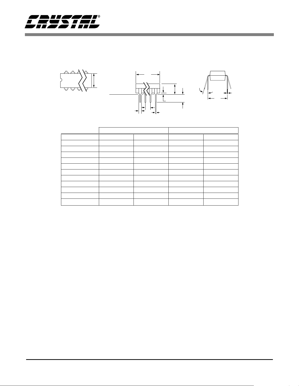
CS5521 CS5523
PACKAGE DESCRIPTIONS
20 PIN PLASTIC (PDIP) PACKAGE DRAWING
D
1
TOP VIEW
DIM MIN MAX MIN MAX
A 0.155 0.180 3.94 4.57
A1 0.020 0.040 0.51 1.02
b 0.015 0.022 0.38 0.56
b1 0.050 0.065 1.27 1.65
c 0.008 0.015 0.20 0.38
D 0.960 1.040 24.38 26.42
E 0.240 0.260 6.10 6.60
e 0.095 0.105 2.41 2.67
eA 0.300 0.325 7.62 8.25
L 0.125 0.150 3.18 3.81
∝
Notes: 1. Positional tolerance of leads shall be within 0.25 mm (0.010 in.) at maximum material condition, in
relation to seating plane and each other.
2. Dimension eA to center of leads when formed parallel.
3. Dimension E does not include mold flash.
E
A1
A
L
∝
eA
SIDE VIEW
c
SEATING
PLANE
b1
e
BOTTOM VIEW
b
INCHES MILLIMETERS
0° 15° 0° 15°
34 DS317PP2
Page 35

24 PIN SKINNY (PDIP) PACKAGE DRAWING
D
1
TOP VIEW
DIM MIN MAX MIN MAX
A 0.155 0.180 3.94 4.57
A1 0.020 0.040 0.51 1.02
b 0.014 0.022 0.36 0.56
b1 0.040 0.065 1.02 1.65
c 0.008 0.015 0.20 0.38
D 1.235 1.265 31.37 32.13
E 0.240 0.260 6.10 6.60
e 0.095 0.105 2.41 2.67
eA 0.300 0.325 7.62 8.25
L 0.125 0.150 3.18 3.81
∝
E
A1
A
L
SEATING
PLANE
b1
e
BOTTOM VIEW
b
INCHES MILLIMETERS
0° 15° 0° 15°
CS5521 CS5523
∝
eA
SIDE VIEW
c
Notes: 1. Positional tolerance of leads shall be within 0.25 mm (0.010 in.) at maximum material condition, in
relation to seating plane and each other.
2. Dimension eA to center of leads when formed parallel.
3. Dimension E does not include mold flash.
DS317PP2 35
Page 36

CS5521 CS5523
20 PIN SSOP PACKAGE DRAWING
N
1
23
TOP VIEW
D
E
e
2
b
SIDE VIEW
A2
A1
A
SEATING
PLANE
L
INCHES MILLIMETERS
1
E1
END VIEW
NOTE
DIM MIN MAX MIN MAX
A -- 0.084 -- 2.13
A1 0.002 0.010 0.05 0.25
A2 0.064 0.074 1.62 1.88
b 0.009 0.015 0.22 0.38 2,3
D 0.272 0.295 6.90 7.50 1
E 0.291 0.323 7.40 8.20
E1 0.197 0.220 5.00 5.60 1
e 0.024 0.027 0.61 0.69
L 0.025 0.040 0.63 1.03
∝
0° 8° 0° 8°
Notes: 1. “D” and “E1” are reference datums and do not included mold flash or protrusions, but do include mold
mismatch and are measured at the parting line, mold flash or protrusions shall not exceed 0.20 mm per
side.
2. Dimension “b” does not include dambar protrusion/intrusion. Allowable dambar protrusion shall be
0.13 mm total in excess of “b” dimension at maximum material condition. Dambar intrusion shall not
reduce dimension “b” by more than 0.07 mm at least material condition.
3. These dimensions apply to the flat section of the lead between 0.10 and 0.25 mm from lead tips.
36 DS317PP2
Page 37

CS5521 CS5523
24 PIN SSOP PACKAGE DRAWING
N
1
23
TOP VIEW
D
E
e
2
b
SIDE VIEW
A2
A1
A
SEATING
PLANE
L
INCHES MILLIMETERS
1
E1
END VIEW
NOTE
DIM MIN MAX MIN MAX
A -- 0.084 -- 2.13
A1 0.002 0.010 0.05 0.25
A2 0.064 0.074 1.62 1.88
b 0.009 0.015 0.22 0.38 2,3
D 0.311 0.335 7.90 8.50 1
E 0.291 0.323 7.40 8.20
E1 0.197 0.220 5.00 5.60 1
e 0.024 0.027 0.61 0.69
L 0.025 0.040 0.63 1.03
∝
0° 8° 0° 8°
Notes: 1. “D” and “E1” are reference datums and do not included mold flash or protrusions, but do include mold
mismatch and are measured at the parting line, mold flash or protrusions shall not exceed 0.20 mm per
side.
2. Dimension “b” does not include dambar protrusion/intrusion. Allowable dambar protrusion shall be
0.13 mm total in excess of “b” dimension at maximum material condition. Dambar intrusion shall not
reduce dimension “b” by more than 0.07 mm at least material condition.
3. These dimensions apply to the flat section of the lead between 0.10 and 0.25 mm from lead tips.
DS317PP2 37
Page 38

Preliminary product inform ati on describes products which are i n prod ucti on, but for which full characterization data is not yet avai l ab le . Advance product information
describes products which are in development and subject to development changes. Cirrus Logic, Inc. has made best efforts to ensure that the information contained
in this document is accurate and reliable. However, the information is subject to change without notice and is provided “AS IS” without warranty of any kind (express
or implied). No responsibility i s assumed by Cirrus Logi c, Inc. for the use of this in formation, nor for i nfringements of pat ents or ot her right s of t hird parties. This
document is the property of Cirrus Logic, Inc. and implies no license under patents, copyrights, trademarks, or trade secrets. No part of this publication may be copied,
reproduced, stored in a retr ieval system, or transmitted, i n any form or by any means (electr onic, mechani cal, photogr aphic, or otherwise ) without t he prior wri tten
consent of Cirrus Logic, Inc. Items from any Cirrus Logic website or disk may be printed for use by the user. However, no part of the printout or electronic files may
be copied, reproduced, stored in a retrieval system, or transmitted, in any form or by any means (electronic, mechanical, photographic, or otherwise) without the prior
written consent of Cirrus Logic, Inc.Furthermore, no part of this publication may be used as a basis for manufacture or sale of any items without the prior written consent
of Cirrus Logic, Inc. The names of products of Ci rrus Logic, Inc. or oth er ven dor s and suppliers appearing i n this document may be trademarks or servi ce marks of
their respective owners which may be registered in some jurisdictions. A list of Cirrus Logic, Inc. trademarks and service marks can be found at http://www.cirrus.com.
 Loading...