

Page 1
Digital Processor / Digital Mixer
SERVICE MANUAL
Models:
IQ-USM 810
Some models may be exported under the name Amcron.
®
©2000 by Crown International, Inc., P.O. Box 1000, Elkhart, Indiana 46515-1000 U.S.A.
Telephone: 219-294-8000. Trademark Notice: Distributed Intelligence™ and IQ for Windows™
are trademarks and Crown®, IQ®, and IQ System
International, Inc. Other trademarks are the property of their respective owners.
®
are registered trademarks of Crown
130447-1
04-00
Rev. A
Page 2
IQ-USM 810 Service Manual
The information furnished in this manual does not include all of the details of design, production, or variations
of the equipment. Nor does it cover every possible situation which may arise during installation, operation or
maintenance. If you need special assistance beyond the scope of this manual, please contact the Crown
Technical Support Group.
Mail: P.O. Box 1000 Elkhart IN 46515-1000
Shipping: Plant 2 SW 1718 W. Mishawaka Road Elkhart IN 46517
Phone: (800) 342-6939 / (219) 294-8200
FAX: (219) 294-8301
130447-1 Rev. A
CAUTION
TO PREVENT ELECTRIC SHOCK DO
NOT REMOVE TOP OR BOTTOM
COVERS. NO USER SERVICEABLE
PARTS INSIDE. REFER SERVICING
TO QUALIFIED SERVICE
PERSONNEL. DISCONNECT
POWER CORD BEFORE REMOVING
REAR INPUT MODULE TO ACCESS
GAIN SWITCH.
WARNING
AVIS
À PRÉVENIR LE CHOC
ÉLECTRIQUE N’ENLEVEZ
PAS LES COUVERTURES.
RIEN DES PARTIES
UTILES À L’INTÉRIEUR.
DÉBRANCHER LA BORNE
AVANT D’OUVRIR LA
MODULE EN ARRIÈRE.
TO REDUCE THE RISK OF ELECTRIC
SHOCK, DO NOT EXPOSE THIS
EQUIPMENT TO RAIN OR MOISTURE!
The lightning bolt
triangle is used to
alert the user to the
risk of electric shock.
II
The exclamation point
triangle is used to alert the
user to important operating
or maintenance instructions.
©2000 Crown International, Inc.
Page 3

130447-1 Rev. A
IQ-USM 810 Service Manual
Revision History
Revision Number
Rev. A
Date
04-2000 Initial Printing
Comments
©2000 Crown International, Inc.
III
Page 4

IQ-USM 810 Service Manual
130447-1 Rev. A
This page intentionally left blank
IV
©2000 Crown International, Inc.
Page 5

130447-1 Rev. A
1 Introduction ............................................................................ 1-1
2 Specifications ......................................................................... 2-1
3 Circuit Theory ........................................................................ 3-1
IQ-USM 810 Service Manual
Table of Contents
1.1 Introduction ................................................................................1-1
1.2 The IQ-USM 810 ........................................................................1-1
1.3 Warranty.....................................................................................1-1
3.1 Overview .................................................................................... 3-1
3.2 Power Supply .............................................................................3-1
3.3 Input ...........................................................................................3-1
3.3.1 Input Analog Processing...................................................3-1
3.3.2 Clock Signals ....................................................................3-2
3.3.3 A/D Conversion .................................................................3-2
3.3.4 DC Voltages ......................................................................3-4
3.4 Output ........................................................................................ 3-4
3.4.1 Clock Buffers.....................................................................3-4
3.4.2 DAC Conversion................................................................3-4
3.4.3 Output Analog Processing................................................ 3-4
3.5 SHARC Processing ....................................................................3-5
3.5.1 +3.3V Power Supply..........................................................3-5
3.5.2 Clocks ...............................................................................3-5
3.5.3 Reset .................................................................................3-5
3.5.4 System Control Interface................................................... 3-5
3.5.5 PLDs.................................................................................. 3-6
3.5.6 Bus Arbitration...................................................................3-6
3.5.7 Bus Utilization....................................................................3-6
3.5.8 DSP Processing ................................................................3-6
3.5.9 Audio Routing....................................................................3-8
3.6 System Controller.......................................................................3-8
3.6.1 Control Processing............................................................ 3-9
3.6.2 RS232.............................................................................. 3-10
3.6.3 Crown Bus Loop..............................................................3-10
3.6.4 Real Time Clock ..............................................................3-10
3.6.5 Front Panel ......................................................................3-10
3.6.6 Control Port .....................................................................3-10
3.7 Front Display ............................................................................3-10
4 Maintenance........................................................................... 4-1
4.1 General Information....................................................................4-1
4.2 Definitions...................................................................................4-1
4.3 Required Test Equipment ..........................................................4-1
4.4 Message String Syntax ..............................................................4-2
©2000 Crown International, Inc.
V
Page 6

IQ-USM 810 Service Manual
4.5 Standard Initial Conditions........................................................4-2
4.6 Test Procedures.........................................................................4-2
4.7 Typical Measurements............................................................... 4-7
4.8 Test/Debug Objects...................................................................4-7
4.9 Display Test Patterns ................................................................. 4-8
4.10 Error Codes..............................................................................4-9
4.11 Troubleshooting FAQs ............................................................. 4-9
5 Parts Information................................................................... 5-1
5.1 General Information ..................................................................5-1
5.2 Ordering and Receiving Parts ..................................................5-1
5.2.1 Terms ..................................................................................... 5-1
5.2.2 Shipment ................................................................................ 5-1
6 Exploded View Parts ............................................................. 6 -1
130447-1 Rev. A
Table of Contents
7 Module and Schematic Information..................................... 7 -1
8 Module Parts.......................................................................... 8-1
PWA 126451-3 ................................................................................. 8-3
PWA 126690-3 ............................................................................... 8-13
PWA 126693-4 ............................................................................... 8-47
PWA 126744-3 ............................................................................... 8-59
PWA 128045-1 ............................................................................... 8-65
PWA 128047-3 ............................................................................... 8-75
PWA 128047-4 ............................................................................... 8-87
PWA 128049-1 ............................................................................... 8-99
PWA 128051-3 ............................................................................. 8-117
9 Schematics ............................................................................ 9-1
VI
©2000 Crown International, Inc.
Page 7

130447-1 Rev . A
1 Introduction
1.1 Introduction
This manual contains complete service information
on the Crown® IQ-USM 810 Digital Processor/Digital
Mixer. It is designed to be used in conjunction with
the Reference Manual; however, some important information is duplicated in this Service Manual in case
the Reference Manual is not readily available.
NOTE: THE INFORMATION IN THIS MANUAL IS
INTENDED FOR USE BY AN EXPERIENCED TECHNICIAN ONLY!
1.2 The IQ-USM 810
The Crown IQ-USM 810 is an 8x10 mixer/processor
that provides unique dual input processing paths. As
an IQ® component, it can be controlled by an IQ Sys-
tem®, and with its distributed intelligence™ capability ,
continue to operate even when an IQ System is not
connected. The IQ-USM 810 can also act as a system interface to other IQ components.
The IQ-USM 810 features high-quality 24-bit A/D and
D/A converters along with 240MIPS of full 32-bit floating point DSP for optimum dynamic range.
The dual input processing paths include a full complement of signal processing features, including advanced algorithms for gating, auto-leveling, filtering,
compression and automixing.
A full 8x8 Matrix Mixer allows any combination of routing and mixing from any input to any output. The Matrix Mixer outputs are routed to the two Main Audio
IQ-USM 810 Service Manual
Outputs and eight AUX Audio Outputs. The Main and
AUX Audio Output sections further process the signal with individually adjustable signal delay and filters along with an Ambient-Leveler and a high performance Output Limiter for system protection.
A Multi-Function Control Port implements analog and
digital I/O for control and monitor by simple potentiometer and switch wall controllers and indicator panels.
All of the IQ-USM 810 parameters are backed up via
reliable FLASH memory. System configurations may
be stored for recall from any of thirty-two system presets from the front panel control or via IQ for Windows
software.
1.3 Warranty
Each Reference Manual contains basic policies as
related to the customer . In addition, it should be stated
that this service documentation is meant to be used
only by properly trained personnel. Because most
Crown products carry a 3-Year Full Warranty (including round trip shipping within the United States), all
warranty service should be referred to the Crown Factory or Authorized Warranty Service Center. See the
applicable Reference Manual for warranty details. To
find the location of the nearest Authorized Warranty
Service Center or to obtain instructions for receiving
Crown Factory Service, please contact the Crown
Technical Suppor t Group (within North America), or
your Crown/Amcron Importer (outside North America).
If you are an Authorized Warranty Service Center and
have questions regarding the warranty of a product,
please contact the Crown Factory Service Manager
or the Crown Technical Suppor t Group.
©2000 Crown International, Inc.
Crown Customer Service
Technical Support Group
Factory Service
Parts Department
Mailing Address: P.O. Box 1000, Elkhart IN 46515
Shipping Address: Plant 2 S. W.
1718 W. Mishawaka Rd., Elkhart IN 46517
Phone: (219) 294-8200
Toll Free: (800) 342-6939
Fax: (219) 294-8301
http://www.crownaudio.com
Introduction 1-1
Page 8
IQ-USM 810 Service Manual
130447-1 Rev . A
Figure 1.1 IQ-USM 810 Front and Rear Views
1-2 Introduction
©2000 Crown International, Inc.
Page 9

130447-1 Rev. A
2 Specifications
General
Front Panel Controls: Front-panel switches select IQ
Address, Baud Rate, factory default preset (P00), and
any of 32 user-defined presets (P01–P32).
Rear-Panel Controls: A 3-position selector switch
(mic/line/phantom) and a calibrated gain control for
each input.
Connectors: Crown Bus: RJ-45 for input/output, RJ-45
for daisy output, RS232: DB9F computer interface for
both component and interface modes. Multi-function
Port: DB37M for analog inputs, digital inputs, digital
outputs, +5VDC, +10VDC and Ground. Audio Inputs
and Outputs: 3-pin male removable barrier block connectors, Euro-style cable connector supplied. AC
Power: IEC320 connector for AC power cord.
Display: A blue front-panel Enable indicator lights to
show that the unit is plugged in and AC power is being
supplied. An amber front-panel Data Signal Presence
Indicator (DATA) flashes whenever commands addressed to the IQ-USM 810 are received. A green
front-panel Interface indicator lights when the IQ-USM
810 is being used as system interface. A three-digit
digital display indicates the IQ-USM 810’s initialization
sequence by displaying each processor’s name as it
comes online, indicates the presently selected preset,
indicates the IQ address and baud rate while those
parameters are being adjusted, indicates when a parameter has been stored in flash memory, and when
any parameter is varied from its value within the currently selected preset. Ladder Display: A front panel,
sixteen-segment LED display matrix can be set to
three different operating modes: Level Meter, Input
Gate Status, and Infinity Pattern.
Power Requirements: 100VAC to 240VAC, 35VA
nominal.
Protection: if communication is lost, the unit will continue to function with the last commands received.
RS232 Data Communication
Baud Rate: Selectable to 19.2 K, 38.4 K, 57.6 K, or
115.2 K BAUD.
Data Format: Serial, binary, asynchronous; 1 start bit;
1 stop bit; 8 data bits; no parity.
Crown Bus Data Communication
Data Rate: 38.4 K BAUD.
Data Format: Serial, binary, asynchronous; 1 start bit;
IQ-USM 810 Service Manual
1 stop bit; 8 data bits; no parity.
Crown Bus Interface Type: Optically isolated 20 mA
current loop.
Operation: Half-duplex.
Transmission Distance: Variable from 200 to 3000
feet (61 to 914 meters), depending upon wire capacitance. Typically 1000 feet (305 meters) using shielded
twisted-pair wire, #26 AWG or larger. Can be extended
with an IQ Repeater.
Audio
Phantom V oltage: +24VDC at 10 mA.
Input Gain Range: +20 dB to –12 dB.
Digital Sampling: 24 bit, 48 kHz.
Input Impedance: 20 k ohms balanced, 10 k ohms
unbalanced.
Dynamic Range: Greater than 100 dB (A-weighted,
20 Hz–20 KHz).
Frequency Response: ± 0.5 dB, 20 Hz–20 kHz.
Common Mode Rejection: 50 dB (typical).
Crosstalk: Greater than 80 dB at 10 kHz.
T otal Harmonic Distortion: Less than 0.05% THD + N
(1 kHz, 0 dBu).
Output Impedance: 100 ohms balanced, 50 ohms
unbalanced.
Max Input Level: +32 dBu (line) or +7 dBu (mic).
Max Output Level: +20 dBu.
Control Port
Power Supply: +5VDC and +10VDC outputs are provided. The total output current is limited to 1A.
Outputs
Logic Low: less than 0.1V.
Logic High: 10V (via internal pull-up).
Output Current is limited to 10mA max per pin.
Inputs
Input Impedance: greater than 50 k ohms.
Logic Low: less than 0.5V.
Logic High: greater than 5V.
Analog Range: 0 to 10V (for inputs 9-16 only).
Max Input Voltage: 25V.
Mechanical
Weight: 13 pounds, 4 ounces (6.1 kg).
Dimensions: 19-inch (483-cm) standard rack mount
width (EIA RS-310-B), 16-inch (40.6-cm) depth behind
mounting surface, and 3.5-inches (8.9-cm) height.
©2000 Crown International, Inc.
Specifications 2-1
Page 10

IQ-USM 810 Service Manual
130447-1 Rev. A
This page intentionally left blank
2-2 Specifications
©2000 Crown International, Inc.
Page 11
130447-1 Rev. A
3 Circuit Theory
3.1 Overview
This section explains operation of the IQ-USM 810 circuitry . Please refer to the IQ-USM 810 Reference Manual
and IQ for Windows help files for information about the
IQ-USM 810 features and operation.
The IQ-USM 810 consists of a universal power supply
and 5 PWAs (see Figure 3.1). Each PW A has a particular function and initial troubleshooting should focus on
attempting to determine which PWA is causing the malfunction. The PWAs are not unit-dependent, so a known
good working PWA or unit can be used to pinpoint which
PWA is faulty.
3.2 Power Supply
The universal power supply used by the IQ-USM 810
resides underneath the System Controller at the back
of the unit. It receives AC input from the IEC filter located on the back panel and supplies +15V, –15V , and
+5VDC to the System Controller . There is a fuse located
on the supply and should be checked if the power supply is suspected. Replace fuse with the same rated
type only.
IQ-USM 810 Service Manual
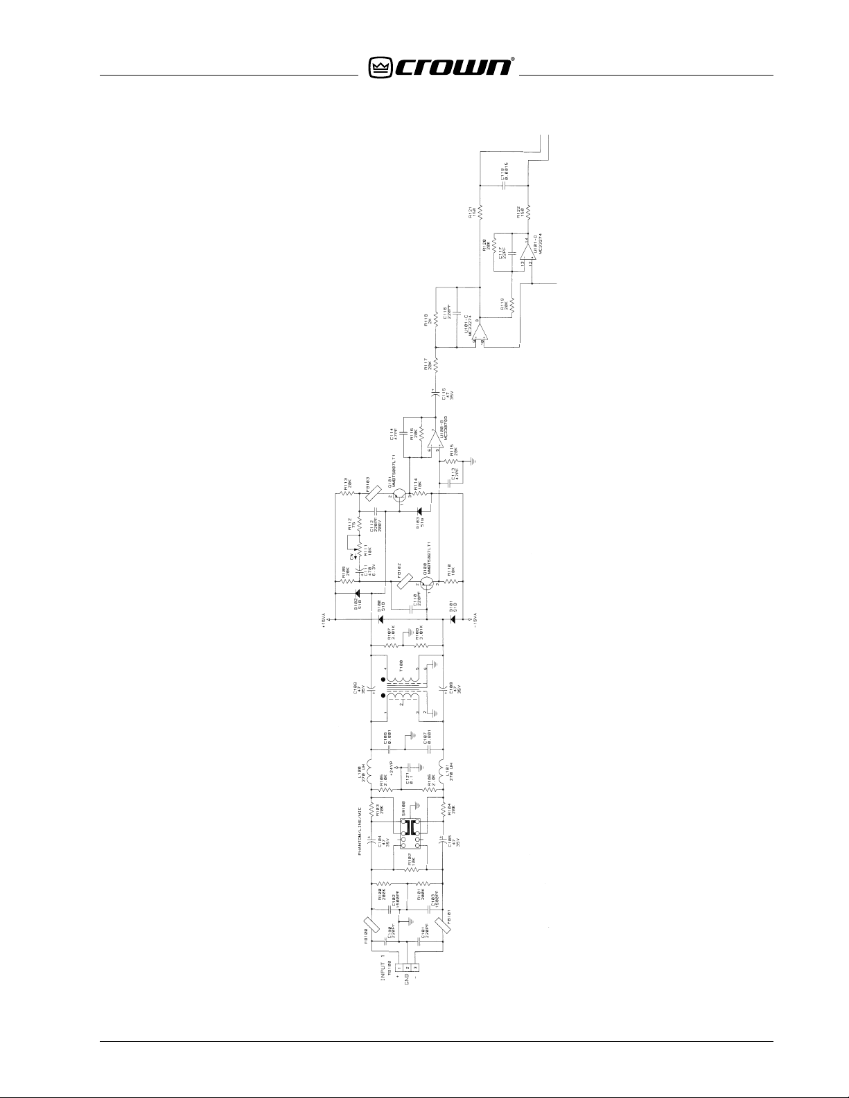
3.3 Input
The input Printed Wire Assembly (PWA) is located at
the back of the unit on the bottom. It offers eight balanced input audio channels via 3 pin connectors. Figure 3.2 shows the block diagram of the input PWA. The
PWA is composed of the following sections: Input Analog Processing, Clock Signals, A/D Conversion, and DC
Voltages.
3.3.1 Input Analog Processing
Each input channel has analog processing that provides filtering, line/mic switching, phantom power, optional input transformer isolation, and variable gain control. The balanced output of each analog channel is fed
to a shared A/D converter.
All eight analog input channels are identical (Figure 3.3).
The balanced analog input is RF filtered by FB100,
FB101, C102, and C103. Capacitors C100 and C101
provide filtering to ensure that no noise from the unit
goes out. R100-102 provide a 10 k ohm balanced input
impedance in the line mode. Switch SW100 provides
switching between Phantom, Line, and Mic modes.
• Phantom: SW100 shorts R103/C104 and R104/
C105 to allow the phantom DC voltage (+24VDC)
to be available on the input connector. In addition, no gain reduction is provided on the input
path. R105 & R106 allows current limiting of the
phantom voltage.
©2000 Crown International, Inc.
Figure 3.1 Overall Block Diagram
Circuit Theory 3-1
Page 12
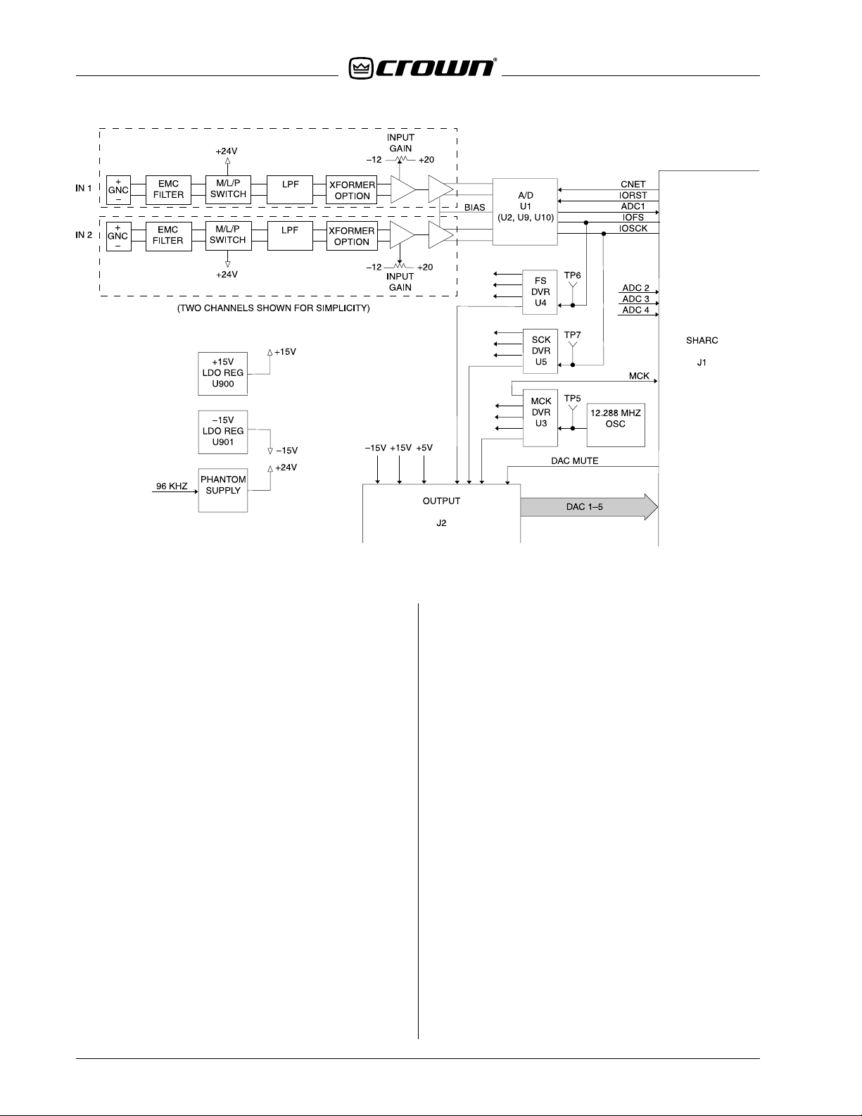
IQ-USM 810 Service Manual
130447-1 Rev. A
Figure 3.2 Input PWA Block Diagram
• Line: In Line mode, both the coupling capacitors
(C104 & C105) and the series resistors (R103 &
R104) are in the signal path. The capacitors block
the phantom voltage from the input while the series resistors work as a voltage divider with R105
& R106 to provide a 17.7x (25 db) reduction in
gain.
• Mic: The coupling capacitors are provided to block
the phantom power, but the series resistors are
shorted, allowing full gain through the input channel.
L100/C106 (L101/C107) provide an additional low-pass
filter. C108 & C109 provide coupling to the variable
gain preamp, except when the optional input isolation
transformer (T100) is in place. Q100 and Q101 form a
differential amplifier whose gain is adjusted by R111.
U100B provides a filtered differential to single-ended
conversion. U101C provides a gain reduction and biases the input signal to +2.2VDC. The output bias voltage of the A/D converter's pin 15 is fed to the op amp to
bias the signal to the A/D's bias point. Lack of voltage
at pin15 is an indication that the A/D converter is either
in reset or is not being clocked.
3.3.2 Clock Signals
The master oscillator for the audio signals is Y1, which
generates a 12.288 MHz signal (256Fs). This clock is
buffered by U3 and provides separate outputs to each
of the A/D converters, the Output PWA for the DAC's,
and to the SHARC PWA for distribution to the optional
CobraNet™ (CNET) PWA.
U1 normally acts as the generator of the Serial Clock
and the Frame Clock. Serial Clock provides the timing
of the serial audio data, 3.032 MHz (64Fs), and Frame
Clock is the actual sampling clock frequency, 48 kHz
(Fs). U1 monitors the CNET line from the SHARC PWA
immediately out of reset. If the pin is low, it acts as a
master source and begins providing Serial Clock and
Frame Clock to U4 & U5 for buffering and distribution. If
U1 senses a high on the CNET pin out of reset, it oper ates in slave mode like the other A/D converters and
waits for Serial and Frame Clocks from the CNET PWA.
3.3.3 A/D Conversion
Each A/D converter processes 2 input channels. Full
scale input signals are 2.82Vp-p and are sampled at a
48-kHz rate with 24-bit resolution. The converters are
reset by the DSP's by the IO_RST line with a low being
reset. The converters provide an I2S 32-bit time-division
multiplexed data audio stream. The most significant 24
bits are linear PCM (two's complement) audio data followed by 8 bits of converter peak hold data that is un-
3-2 Circuit Theory
©2000 Crown International, Inc.
Page 13
130447-1 Rev. A
IQ-USM 810 Service Manual
©2000 Crown International, Inc.
Figure 3.3 Input Analog Processing Circuitry (one channel)
Circuit Theory 3-3
Page 14
IQ-USM 810 Service Manual
130447-1 Rev. A
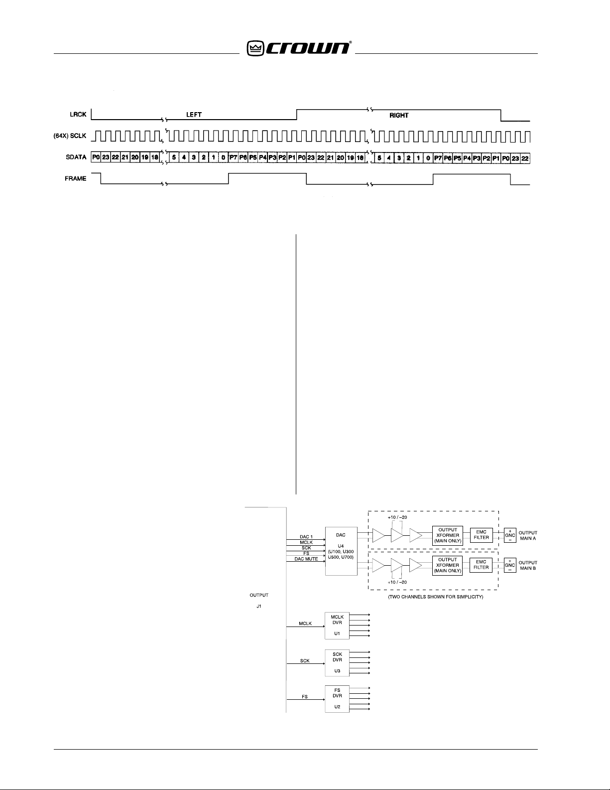
Figure 3.4 Audio Data and Clock Signals
used. This data is routed to the SHARC PWA for processing (ADC1-4). Figure 3.4 shows the audio data and
its relationship to the clock signals.
3.3.4 DC Voltages
The Input PWA receives +/–15V and +5V fr om the System Controller . +15V from P900 is filtered and then r egulated by a low dropout regulator, U900. R900 & R901
set the output voltage of the regulator at +14.5V. The
–15V is processed similarly by U901. The +5V is filtered
separately for the digital portion of the PWA than the
analog side.
The phantom power voltage is generated by U902. +15V
from P900 drives L904 while Q900 acts as a switch to
charge L904. R905 acts as a current sense and limits
the output current of the phantom power by reducing
the voltage at currents over 50 mA. R904 & R908 set
the output voltage at about +26V. U902 is driven from a
96-kHz clock provided by U10. This ensures that the
switching supply is synced to the sampling frequency
of the converters (2Fs). During reset, U902 will run at a
slightly lower frequency due to the lack of an input clock.
3.4 Output
The Output PWA sits on top of the Input
PWA and provides 10 audio outputs; Main
A/B and AUX 1-8. The Output PWA receives all of its signals from the Input PWA
via a 26-pin ribbon cable. Functionality
can be divided into Clock Buffers, DAC
Conversion, and Output Analog Processing. A block diagram of the Output PWA
is shown in Figure 3.5.
Each DAC takes a 2 channel I2S 32-bit time-division
multiplexed data audio stream from the SHARC PWA
and converts it at a 24-bit, 48-kHz rate (Figure 3.4). Like
the A/D converter, the audio output of the DAC is biased positive by 2.2V and a full signal is 2.82Vp-p.
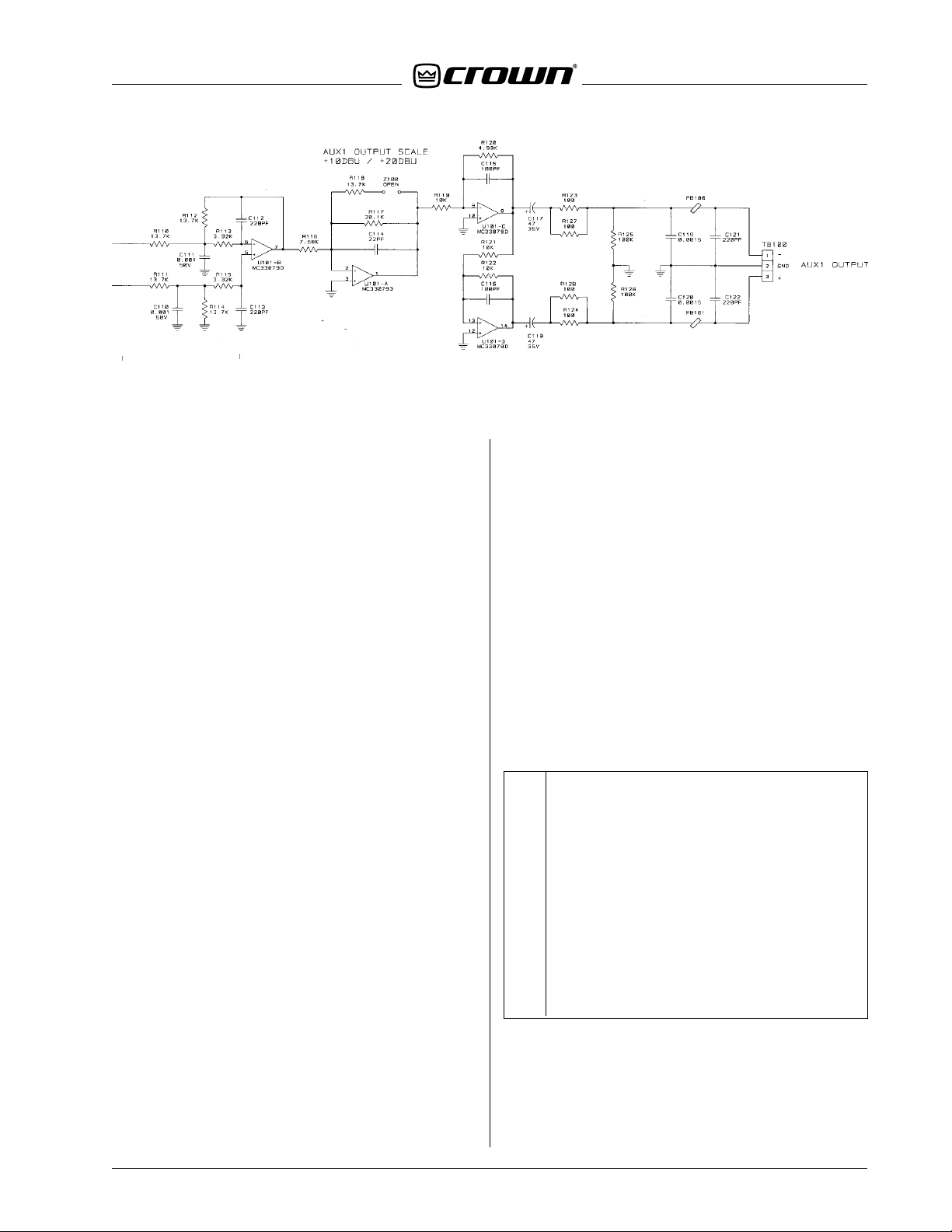
3.4.3 Output Analog Processing
All ten analog output channels are identical (Figure 3.6).
The balanced output of the DAC drives a unity gain
amplifier that also filters the audio signal. The singleended output is fed to U101A which provides gain of
either 1.2 (+10 dbu) or 3.9 (+20 dbu). Z100 is normally
open, which provides a +20 dbu output for a full scale
signal from the DAC. U101C provides a gain reduction
of 2, then U101D inverts the signal and provides the
other balanced output. An output impedance of 50 ohms
is provided by the series resistors while the output ferrite bead provides RF filtering to ensure isolation. Optional isolation transformers are available on the Main
outputs by removing the series resistors and placing
the transformers.
3.4.1 Clock Buffers
Three clock buffers, U1-3, accept the Master (12.288 MHz), Serial (3.032 MHz), and
Frame (48 kHz) clocks from the Input PWA
and provide separate outputs to each of
the five DAC's.
3.4.2 DAC Conversion
3-4 Circuit Theory
Figure 3.5 Output PWA Block Diagram
©2000 Crown International, Inc.
Page 15
130447-1 Rev. A
IQ-USM 810 Service Manual
Figure 3.6 Output Analog Processing Circuitry (one channel)
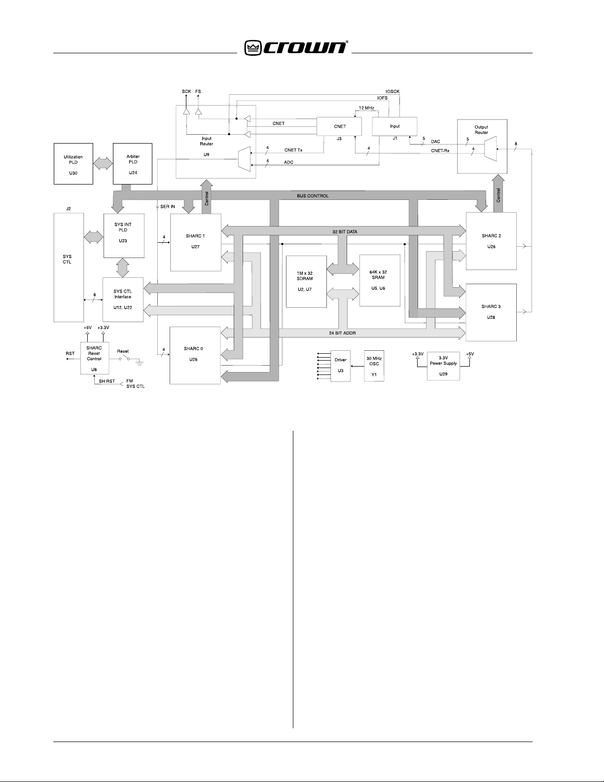
3.5 SHARC Processing
The SHARC PWA sits in the center of the chassis and is
the DSP engine that provides all of the signal processing for the unit. At the core of this processing is four
Analog Devices ADSP-21065L SHARC 32-bit floating
point DSP's running at an internal rate of 60 MHz. Full
speed SDRAM interface is provided. Figure 3.8 shows
the block diagram of the SHARC PWA. Features include
a +3.3V Power Supply, Clocks, Reset, System Controller Interface, PLD's, Bus Arbitration, Bus Utilization, DSP
Processing, and Audio Routing.
3.5.1 +3.3V Power Supply
The entire SHARC PWA utilizes +3.3V by taking the +5V
from P1 and converts it to +3.3V using a 300-kHz switching supply IC, U29. Q2 & Q3 work with U29 to control
the charging of L1. R200 current senses the supply for
overload protection. C27 & C113 provide output filtering of the supply.
3.5.2 Clocks
Oscillator Y1 provides a 30-MHz clock to buffer U3 for
distribution to all SHARC's, SRAM, and other circuitry.
3.5.3 Reset
U8 monitors both the +5V and +3.3V power supplies
and places the SHARC's into reset if either supply
droops. In addition, the System Controller uses U8 to
reset the SHARC's using pulldown via D1. Switch S1
allows manual reset of the SHARC's for troubleshooting. Q1 monitors the reset line to the SHARC's and lights
LED E5 when the SHARC's are not in reset. The active
low \RST line resets all four SHARC's and the PLD's
(U9, U11, U23, U24, and U30).
3.5.4 System Controller Interface
Communications between the System Controller and
SHARC processors occurs through a series of latches
(U12-22) that provide address and data. PLD U23 re-
ceives commands from the System Controller (SH_A02, \HCS, HR/W) to load data and addresses into these
latches. Once the data is in the latches, U23 communicates with Arbiter PLD U24 (\SYSBR, \SYSBG, \RD, \WR)
to request access to the SHARC bus.
There are no non-volatile memory resources on the
SHARC PWA, so the System Controller stores the
SHARC firmware and downloads it during boot. The
System Controller boots each SHARC in succession by
loading code into SRAM and into each SHARC via the
Interface. Once all four SHARC have been booted, they
are allowed to begin audio processing.
If the System Controller encounters any problems during the boot process, it will display an error code on the
front panel display . These er ror codes are shown in the
table in Figure 3.7:
E1 UART f ailed system controller po wer-on self test
E2 RAM failed system controller power-on self test
E3 Application code in flash failed CRC test
E4 Flash verify error
E5 Unrecoverab le firmw are error
E10 SHARC 0 interface hardware error (timeout, etc.)
E11 SHARC 1 interface hardware error (timeout, etc.)
E12 SHARC 2 interface hardware error (timeout, etc.)
E13 SHARC 3 interface hardware error (timeout, etc.)
E22 SHARC 0 software watchdog timeout
E23 SHARC 1 software watchdog timeout
E24 SHARC 2 software watchdog timeout
E25 SHARC 3 software watchdog timeout
Figure 3.7 System Controller Error Codes
Note: Errors 1-9 are for power-up self test and other
miscellaneous errors. Errors 10-25 are err ors related to
the SHARC subsystem.
©2000 Crown International, Inc.
Circuit Theory 3-5
Page 16
IQ-USM 810 Service Manual
130447-1 Rev. A
Figure 3.8 SHARC PWA Block Diagram
The System Controller will display the error code, then
begin the boot process again. By watching the boot
process on the front display , the error code can be r ead
at the end of the boot process before the next boot begins.
3.5.5 PLDs
There are five Programmable Logic Devices (PLD) on
the SHARC PWA (U9, U11, U23, U24, and U30). These
IC's are programmed on the PWA and can be reprogrammed. They have common control and clock lines
(ETCK, ETMS) and are daisy-chained by having each
output (TDO) tied to the next PLD's input (TDI). P3 allows connection to the external PLD programmer.
3.5.6 Bus Arbitration
The 32-bit data and 24-bit address busses of the SHARC
PWA are shared between the System Controller and
the four SHARC processors. Shared SRAM memory
(U5-6) is also available to all processors. The Arbiter
PLD, U24, polices which has access to the bus through
the use of control signals such as bus requests (\HBR,
\SYSBR, \BR0-3), bus grants (\HBG, \SYSBG, \BG0-3),
and SHARC chip selects (\CS0-3). It regulates which
and when each processor has control of the bus to ensure there is no contention.
3.5.7 Bus Utilization
The Arbiter PLD also works with the Bus Utilization PLD,
U30, to monitor each SHARC processor and determine
how much of the available SHARC bus bandwidth each
is using. The Arbiter tells the Utilization PLD on an individual bus cycle basis when each SHARC is on the bus
(UTILIN0-5) and this information is fed to the individual
SHARC's pulse width modulation inputs (UTILOUT0-3)
for calculation of bus access time. This information is
then reported to the System Controller when requested.
3.5.8 DSP Processing
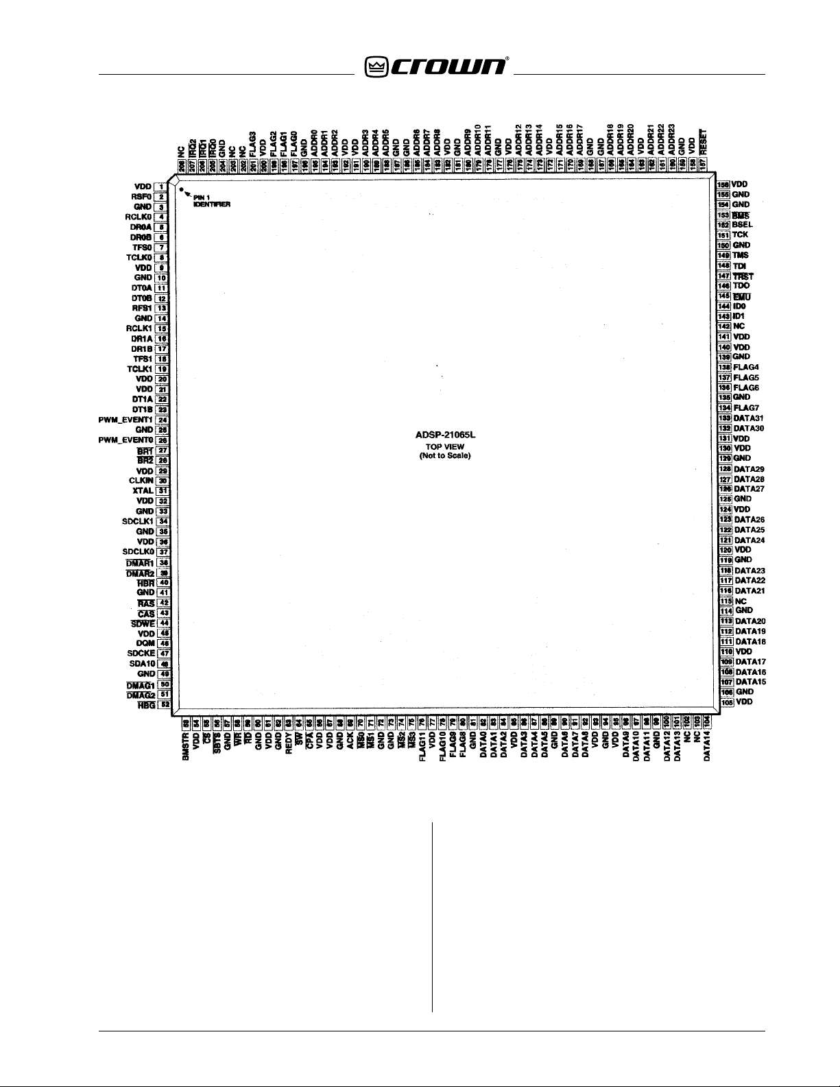
As stated, the four SHARC processors (U25-28) are the
core of the DSP engine. These processors are 208-pin
Plastic Quad Flat Packs (PQFP) and the pinout is shown
in Figure 3.9.
Each SHARC has a specific task in the audio processing chain. SHARC 0 (U25) processes the input audio
for channels 1-4, while SHARC 1 (U27) is tasked with
the input audio processing for channels 5-8. T wo channel serial audio data from the Input Router, U9, is sent
to the appropriate SHARC's serial port along with audio
clock signals Serial Clock (SCK) and Frame Clock (FS).
The input audio is stored by the SHARC until 16 samples
are accumulated, then this audio “brick” is processed.
3-6 Circuit Theory
©2000 Crown International, Inc.
Page 17
130447-1 Rev. A
IQ-USM 810 Service Manual
Figure 3.9 SHARC Pinout
The time allotted for the SHARC to process this audio
data is 330us (16 samples x 48-kHz). At that point the
next audio brick has been collected and is ready for
processing. The processed output audio brick is then
deposited into SRAM (U5, U6). The audio bricks are
then taken by the Output SHARC's for mixing and output processing. SHARC 2 (U26) processes Main A and
Outputs 1-4 while SHARC 3 (U28) is responsible for
Main B and Outputs 5-8. If additional delay is required,
the bricks are allowed to remain in SDRAM before pr ocessing. The minimum delay through the audio processing is as follows:
©2000 Crown International, Inc.
• A/D Conversion 667us
• 5x "brick" delay 1667us
• DAC Conversion 520us
• Total Delay 2854us
This delay is constant and not dependent upon the
particular processing being done.
SDRAM provides a high speed synchronous memory
resource. Only the four SHARC processors have access to SDRAM and they are responsible for the access and maintenance of it. Each SHARC monitors the
Circuit Theory 3-7
Page 18
IQ-USM 810 Service Manual
130447-1 Rev. A
bus and accesses SDRAM when it is available. The
SHARC blocks access to the bus through the use of
the \SDLOCK pin during SDRAM transfers. SDRAM is
utilized only for audio delay processing and has no firmware. If audio is available at the input SHARC's, but is
not being seen by the output SHARC's, a good place to
begin troubleshooting would be with SDRAM.
The System Controller periodically accesses the
SHARC's to query about meter data. As discussed, the
System Controller utilizes the Interface to ask and receive this data.
3.5.9 Audio Routing
Serial audio from the Input PWA is sent to the SHARC
PWA for processing. ADC1-4 is fed to PLD U9 for r outing to the input SHARC's, U25 & U27. Serial digital audio from the optional CobraNet PWA is also available
as CNET_TX1-4. The Input Router sends the appropriate serial audio data to the input SHARC's as directed
by the System Controller via SHARC 1. A serial control
link (IN_MOSI, IN_SPICK) tells the Input Router which
of the serial digital inputs are to be sent to each SHARC's
serial ports.
The Input Router is also responsible for buffering the
audio clocks. By sensing the CNET input from the CNET
PWA, the Input Router can tell if the CNET PW A is con-
nected. If CNET is available, the CNET PWA is responsible to provide the Serial and Frame Clocks. The PLD
accepts the CNET audio clocks and routes them to the
SHARC's and Input PWA. If the CNET PWA is not connected, the audio clocks from the Input PWA are accepted and routed to the SHARC's.
The Output Router , U11, is r esponsible for sending the
serial audio outputs of the output SHARC's to the appropriate place. Five output lines, DAC1-5, allow 10
audio channels to be sent to the Output PWA for DAC
conversion. In addition, four output lines, CNET_RX1-4,
allow 8 audio channels to be directed to the optional
CNET PWA for inclusion onto the CNET system. The
Output Router is programmed by SHARC 2 via
OUT_MOSI & OUT_SPICK.
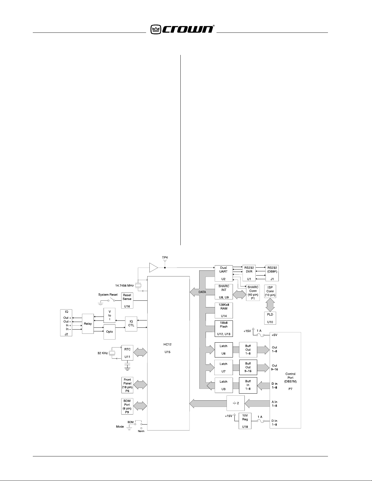
3.6 System Controller
The System Controller PWA sits on the one side of the
chassis and is supported over the power supply. It is
responsible for the coordination and communication with
the outside world, non-volatile memory storage of all
code, and various other functions. The System
Controller's tasks includes Control Processing, RS232,
Crown Bus loop, Real-Time Clock, Front Panel, and
Control Port. Figure 3.10 shows a block diagram for the
System Controller PWA.
3-8 Circuit Theory
Figure 3.10 System Controller Block Diagram
©2000 Crown International, Inc.
Page 19
130447-1 Rev. A
IQ-USM 810 Service Manual
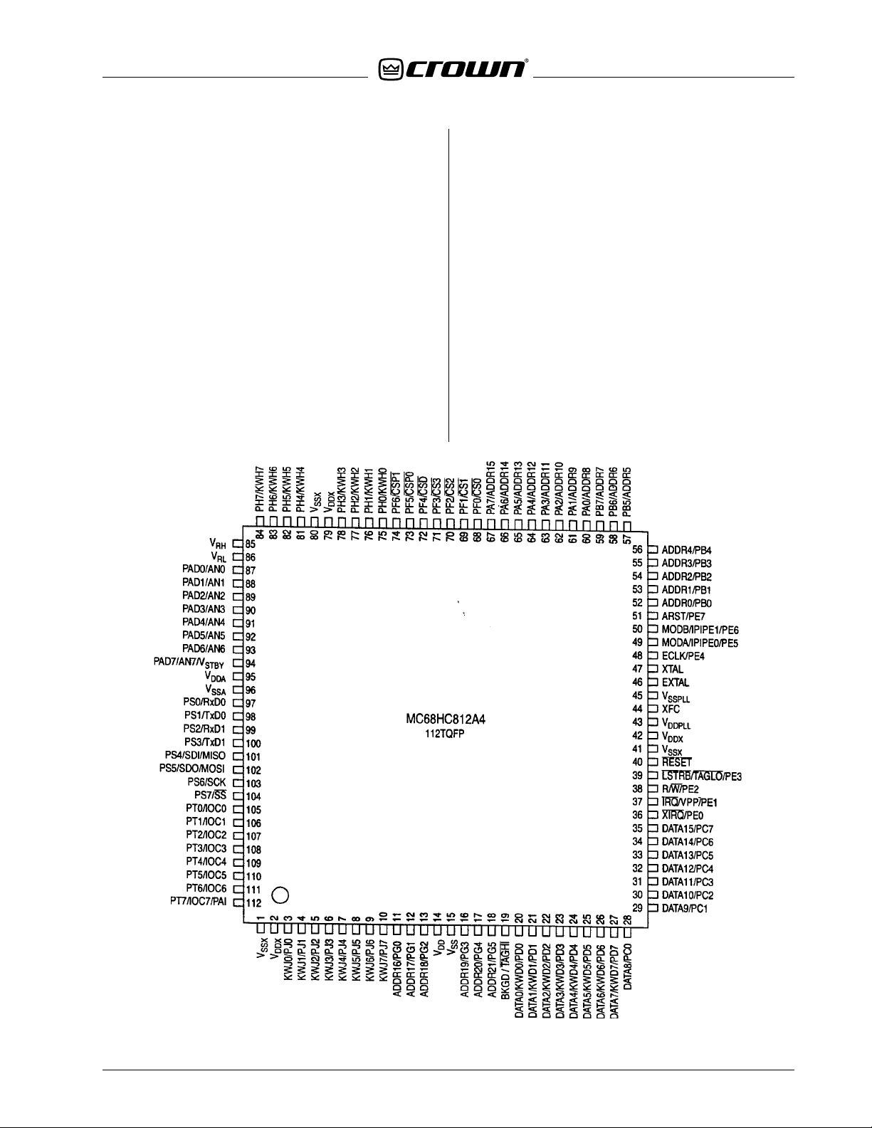
3.6.1 Control Processing
The brain of the System Controller PWA is the Motor ola
68HC12 microcontroller, U15. The 112pin QFP pinout
is shown in Figure 3.11.
The HC12 has a Background Debug Mode (BDM) connection that allows access to the internal workings of
the microcontroller . By connecting a pod to P9 and placing the HC12 in BDM mode, the HC12 can be accessed.
This function is not used in normal operation or troubleshooting, and the BDM jumper should be left in the
NORM position.
The HC12 provides all of the processing for the contro l
of the IQ-USM 810. U16 provides sensing of the +5V
power supply and brings the HC12 out of reset once
the supply is stable. Switch S1 allows resetting of the
controller externally . Q17 monitors the reset line and LED
E1 is lit whenever the processor is not in reset.
Crystal Y2 provides the 14.7456-MHz clock for the
HC12. The clock is buffered by U5D and is provided to
dual UART U2 for baud rate creation.
When the HC12 comes out of reset, it looks to the flash
memory (U13) and begins its boot process. Due to the
slow response of flash memory, normal code processing is carried out in SRAM. The HC12 copies its firmware out of flash memory into SRAM (U14) and once
complete, jumps to SRAM and begins code processing. The HC12 initializes the dual UART and looks for a
break on the RS232 input. If a break is detected, it activates its loader routine and waits for 'S' records from
the RS232 port to be downloaded to flash memory. This
process allows external programming of firmware revisions.
If no break is detected, the HC12 begins loading the
SHARC firmware from flash memory into SHARC
memory via the System Controller Interface. U8 and U9
provide buffering to the SHARC PW A via P1.
©2000 Crown International, Inc.
Figure 3.11 68HC12 microcontroller Pinout
Circuit Theory 3-9
Page 20

IQ-USM 810 Service Manual
130447-1 Rev. A
The HC12 firmware uses a real time operating system
(RTOS) to make efficient use of the HC12's processing
capability. Various tasks are given priorities, and the
RTOS supervises what task has control of the processor at any particular time.
3.6.2 RS232
As mentioned, the RS232 port is used to load firmware
into flash memory. UART U2 provides the serial port
interface to the HC12. The baud rate is programmed
by the HC12 as directed by the front panel (19.2 k to
115 kbps) and the clock is generated from the 14-MHz
clock. The 8-bit parallel interface to the UART is controlled by the U_RD (read), U_CS (chip select), and
FLSH_WE (write) lines. Internal registers control various functions such as baud rate, fifo usage, etc. The
serial I/O of the UART is buffered by RS232 Tx/Rx driver
U1. This buffer takes the +5V and creates the +/–12V
needed for RS232 levels. These signals are available
on the DB9F connector, J1, which is available on the
back panel of the chassis.
The other half of dual UART U2 is used as a serial inter face to the optional CNET PWA. It connects to the CNET
PWA via SHARC connector P1.
3.6.3 Crown Bus Loop
The HC12 has two serial ports and one of them is used
for the interface to the Crown Bus loop hardware. This
is a fixed 38.4-kbps baud rate and uses a dual RJ45
connector J2 to the back panel. In normal operation,
data detected at the input of the Crown Bus loop hardware is sent back out via U19A & B, U20B, and U21A.
When the HC12 wants to communicate, MSTR0 is pulled
high and the TX0 goes out to the Crown Bus loop. R142
provides 20 mA of current to the OUT+ line during nor mal operation. Communication occurs by interrupting
the OUT– path via D4 and U21A.
The input of the Crown Bus loop is buffered by
optoisolator U17 which senses the 20-mA current and
sends the signals to the HC12 (RX0) and directs it back
out the Crown Bus loop via U19A.
Relay K1 provides paths to the I/O circuitry while the
IQ-USM 810 is powered. When the unit is turned off, the
relay allows the Crown Bus loop to pass through the
unit to prevent Crown Bus loop communication from
being interrupted.
3.6.4 Real Time Clock
U11 is a Real Time Clock (RTC) IC that provides timing
to the HC12 for scheduling of real time events. U11 has
an internal oscillator provided by 32-kHz crystal Y1. The
HC12 communicates with the RTC via a serial interface
composed of RTCLK (serial clk), RTC (data), and
RTC_CS (chip select) and periodically queries the RTC
to get or set the time.
Capacitor C25 is a 1F supercap that allows the RTC to
continue to keep time after the unit is powered down.
The RTC senses the loss of power and automatically
switches to the capacitor to provide power . The capacitor can keep the RTC running for up to 45 days without
external power. While the unit is power ed, the RTC trickle
charges the capacitor.
3.6.5 Front Panel
The HC12 interfaces the Front Display PWA via P6. The
three front panel switches are sensed by the HC12 and
display of the front panel LED's are controlled via a serial interface; SCK, MOSI, MISO, and LED_CS. Two display IC's on the Front Display PWA interface both the
discrete LED's and the triple 7-segment display.
3.6.6 Control Port
The control port interface allows external signals or
events to control objects within the box. Additionally,
outputs allow signaling of object status to the outside.
The DB37M connector P7 provides back panel access.
+5V, +10V, and GND is also provided via the connector. Regulator U18 takes the +15V and provides +10V
out. The external power is protected by resettable fuses
limited to 1 A.
The HC12 interfaces the output buffers through latches
U6 and U7. These 16 outputs drive NPN transistors that
provide 10V @ 10 mA to the outside. Ferrite beads and
transient voltage suppressors (TVS) protect the output
circuits.
The digital inputs are buffered by NPN transistors that
allow current drive of the inputs. V oltages up to +25VDC
can be used to drive these inputs. The transistor buffers drive a latch that the HC12 polls to collect the input
status. U4 is used by the HC12 to address the particular I/O latch it wishes to query .
The analog inputs allow a 0 to +10VDC input to be digitized by the HC12's eight 8-bit A/D converters. A voltage divider ensures that the HC12's inputs will not be
overdriven.
3.7 Front Display
The Front Display PWA has the three front panel
switches, triple 7-segment display, Input Status LED's,
Enable, Data, and Interface LED's. The three switches
are sensed and processed directly by the HC12 on the
System Controller PWA. The two IC's, U1 & U2, contr ol
all of the front panel LED's by switching the LED's at a
20%, 1-kHz rate. The serial control from the HC12 tells
the IC's which LED's to light.
3-10 Circuit Theory
©2000 Crown International, Inc.
Page 21
130447-1 Rev . A
4 Maintenance
4.1 General Information
This chapter provides test procedures to be used to
verify operation of this IQ component. Minimum specifications for proof of performance are given with each
procedure. Procedures are in suggested format and
the exact test need not be performed; however, the test
conditions and results must be verified for proof of per formance. These tests, though meant for verification
and alignment, may also be very helpful in troubleshooting. For best results, the tests should be performed in
order.
4.2 Definitions
• IQ Ucode Protocol: The Protocol used by IQ2 products for communication on the Crown IQ Bus.
• DA: IQ Ucode Device Address. A part of the Ucode
string that identifies it as pertaining to a particular
device. The DA for the IQ-USM 810 is set by the
front panel controls. At first power up the IQ-USM
810 defaults to address $01.
• DT: IQ Ucode Device Type Identifier. A part of an
Ucode string that identifies it as pertaining to a
particular type of Ucode component. The DT for
the IQ-USM 810 is $19.
• AK: IQ Message Acknowledgment. This byte is
present in all Ucode device to host messages. It
indicates if the last host to device message was
correctly formatted.
IQ-USM 810 Service Manual
• CT: IQ Message data byte count. A part of the IQ
string that indicates the number of bytes in its
message portion. Note: This byte is automatically
inserted when using IQ Util in enhanced mode.
• CS: Ucode Message Checksum. The last byte of
a Ucode string containing the check sum of the
entire message. Note: This byte is automatically
inserted when using IQ Util in enhanced mode.
4.3 Required Test Equipment
Audio sine-wave generator (Output amplitude accuracy
better than ±0.5 dB)
Oscilloscope
Audio THD+N analyzer
True RMS AC voltmeter
DC voltmeter
Audio multiplexer (balanced) or other means of switch-
ing the audio generator to the eight mixer inputs.
Audio multiplexer (balanced) or other means of switch-
ing the ten mixer outputs to the Audio analyzer and RMS
voltmeter.
PC running applicable IQ Ucode compatible software
Crown IQ Interface IQ-INT II or equivalent
Crown IQ standard 2000' test cables
Method of generating TTL Control Port inputs.
Method of generating analog Control Port inputs.
Method of measuring the Control Port outputs.
Method of measuring the phantom power outputs.
©2000 Crown International, Inc.
WARNING
Circuitry is ESD sensitive. When servicing
the IQ component, the technician must have
approved ESD protection. Proper grounding straps and test equipment are required.
Failure to use proper protection will result
in component failure.
Maintenance 4-1
Page 22

IQ-USM 810 Service Manual
130447-1 Rev . A
4.4 IQ Message String Syntax
4.4.1 Host to Device Messages
The following syntax is used for host to device messages:
Send: XX XX XX XX XX; Description
XX: A byte of the message explicitly given in hexadeci-
mal.
XX: A byte of the message as defined by the two-letter
codes in Section 4.2.
Description: A short phrase to indicate the function of
the message string. The description is added for refer ence only . It is not sent as part of the Ucode message.
4.4.2 Device to Host Messages
The following syntax is used for device to host messages.
Return String: XX XX XX XX XX
XX: A byte of the message explicitly given in hexadeci-
mal.
XX: A byte of the message as defined by the two-letter
codes in Section 4.2.
XX: A byte of the returned message that requires range
testing in accordance to the associated test.
4.5 Standard Initial Conditions
The following tests assume this setup unless stated otherwise.
Unit under test built and programmed as documented,
less top cover and labels.
Preset 32 loaded
Inputs set to line mode.
Input potentiometers set to 0 dB.
Unit under test powered by 120VAC
Unit under test connected to test computer via the
RS232 connector with constant IQ communication at
115.2 K baud.
Output Impedance of Audio Sine-wave Source: 50 W
balanced.
Audio Output Load: ≥10 kW balanced.
4.6 Test Procedures
4.6.1 LOAD PRESET 32
Note: Preset 32 is the factory default test preset. This preset
sets the audio paths straight through (no gain, filters, or processing) to their respective AUX outputs . Main outputs A and
B are driven from inputs 1 and 2 respectively.
Procedure:
Send the select preset 32 command:
Send: DA DT CT B2 7F 09 20 CS; Select preset 32
Send the load preset command:
Send: DA DT CT B4 7F 09 01 CS; Load preset
Note: The load preset command m ust be sent within appro ximately 2 seconds of the select preset command.
Note: Preset 32 may also be selected using the front panel
controls.
1) Use the “∧” and “∨” buttons to select preset 32. (Display shows P32.)
2) Press “SEL” button.
4.6.2 OUTPUT NOISE
Spec: LINE mode: ≤ –75 dBu and ≥ –80 dBu, 22 Hz to
22 kHz bandwidth.
Note: The test and printed specifications do not match. The
printed specifications are for an "A" weighted 20-Hz to 22-kHz
bandwidth. Production tests do not use "A" weighted filtering.
Initial Conditions: Inputs terminated at ≤ 50 W bal-
anced. Bandwidth = 22 Hz to 22 kHz.
Procedure: Verify each main and AUX output meets
spec.
4.6.3 FREQUENCY RESPONSE
Spec: +0.1, –0.6 dB from 20 Hz to 20 kHz.
Initial Conditions: Normalized to a reference of a
1 kHz, 0 dBu signal.
Procedure:
Verify each main and AUX output meets spec with one
of the following methods:
A 10+ point, logarithmically spaced, sweep.
Testing at these frequencies: 20 Hz, 100 Hz, 500 Hz
1 kHz, 5 Hz, 10 kHz, and 20 kHz.
4.6.4 HARMONIC DISTORTION
Spec: < 0.030 % and > 0.001 % THD+N, with a 22 Hz
to 22 kHz bandwidth.
Initial Conditions: Input signal: 1 kHz, 0 dBu.
Procedure: Verify each main and AUX output meets
spec.
4.6.5 COMMON MODE REJECTION
Spec: >40 dB at 60 Hz in line mode, 22 Hz to 22 kHz
bandwidth.
Procedure:
Input a 60 Hz +18 dBu balanced signal.
Monitor the associated AUX output with a 22 Hz to
22 kHz bandwidth and set the reference.
Change the input to common mode (same frequency
and amplitude)
Verify the associated AUX output is attenuated at least
40 dB below reference with a 22 Hz to 22 kHz bandwidth.
4-2 Maintenance
©2000 Crown International, Inc.
Page 23

130447-1 Rev . A
IQ-USM 810 Service Manual
4.6.6 HEAD ROOM / INPUT CLIP LEVEL
Spec: < 1 % THD+N, with a +19.9 dBu input signal.
Initial Conditions: Input signal: 1 KHz, +19.9 dBu.
Procedure: Verify each main and AUX output meets
spec.
4.6.7 INPUT POTENTIOMETER
Spec: ± 2 dB at the –12, and +20 dB settings.
Initial Conditions: Input signal: 1 kHz, 0 dBu in to all
inputs.
Procedure: Verify each input potentiomenter by
perfoming the following:
Set all potentiometers full counter clockwise.
Verify each AUX output is –13 ±2 dBu.
Set potentiometer full clockwise.
Verify each AUX output is +20.5 ±2 dBu.
Return potentiometer to the zero setting.
4.6.8 PHANTOM SUPPLY
Spec: 25.75 ±1VDC unloaded, between each signal pins
(+, –) and chassis ground.
Initial Conditions: Remove all input signals and
impedences. Set all inputs to phantom mode.
Procedure: For each input, Verify the DC voltage on
the “+” and “–” pins referenced to chassis ground pin
on all audio inputs.
4.6.9 CONTROL PORT OUTPUT VOLTAGE PINS
Spec: Pins at rated voltage ±10%.
Procedure:
.
Verify voltage between pins 9 and 10 of the contr ol port
is 5 ±0.25VDC.
Verify voltage between pins 29 and 28 of the control
port is 10 ±0.5VDC.
4.6.10 CONTROL PORT LOGIC INPUTS
Spec: TTL level inputs are detected on the control port
inputs.
Procedure:
Inject a TTL high on the odd numbered control port logic
inputs (IN1, IN3, IN5, and IN7) and leave the even numbered inputs open.
Use the following commands to read the control port
inputs and verify the odd numbered inputs return $01
and the even inputs return $00:
Send: DA DT CT 80 50 0A CS; Get Control Port Digital
Input 1
Return String: DA DT AK CT 80 50 0C IN1 CS
Send: DA DT CT C0 50 0A CS; Get Control Port Digital
Input 2
Return String: DA DT AK CT C0 50 0C IN2 CS
Send: DA DT CT 80 51 0A CS; Get Control Port Digital
Input 3
Return String: DA DT AK CT 80 51 0C IN3 CS
Send: DA DT CT C0 51 0A CS; Get Control Port Digital
Input 4
Return String: DA DT AK CT C0 51 0C IN4 CS
Send: DA DT CT 80 52 0A CS; Get Control Port Digital
Input 5
Return String: DA DT AK CT 80 52 0C IN5 CS
Send: DA DT CT C0 52 0A CS; Get Control Port Digital
Input 6
Return String: DA DT AK CT C0 52 0C IN6 CS
Send: DA DT CT 80 53 0A CS; Get Control Port Digital
Input 7
Return String: DA DT AK CT 80 53 0C IN7 CS
Send: DA DT CT C0 53 0A CS; Get Control Port Digital
Input 8
Return String: DA DT AK CT C0 53 0C IN8 CS
Inject a TTL high on the even numbered control port
logic inputs (IN2, IN4, IN6, and IN8) and leave the odd
numbered inputs open.
Use the above commands to read the control port inputs and verify the even numbered inputs return $01
and the odd inputs return $00.
4.6.11 CONTROL PORT LOGIC OUTPUTS
Spec: Control Port Logical Outputs individually switch
between On and Off.
Procedure:
Use the following commands to set the odd control port
logical outputs and the even outputs off:
Send: DA DT CT 80 58 09 01 CS; Set Control Port Digital Output 1 On.
Send: DA DT CT C0 58 09 00 CS; Set Control Port Digital Output 2 Off.
Send: DA DT CT 80 59 09 01 CS; Set Control Port Digital Output 3 On.
Send: DA DT CT C0 59 09 00 CS; Set Control Port Digital Output 4 Off.
Send: DA DT CT 80 5A 09 01 CS; Set Control Port Digital Output 5 On.
Send: DA DT CT C0 5A 09 00 CS; Set Control Port Digital Output 6 Off.
Send: DA DT CT 80 5B 09 01 CS; Set Control Port Digital Output 7 On.
Send: DA DT CT C0 5B 09 00 CS; Set Control Port Digi-
©2000 Crown International, Inc.
Maintenance 4-3
Page 24

IQ-USM 810 Service Manual
130447-1 Rev . A
tal Output 8 Off.
Send: DA DT CT 80 5C 09 01 CS; Set Control Port Digi-
tal Output 9 On.
Send: DA DT CT C0 5C 09 00 CS; Set Control Port Digi-
tal Output 10 Off.
Send: DA DT CT 80 5D 09 01 CS; Set Control Port Digi-
tal Output 11 On.
Send: DA DT CT C0 5D 09 00 CS; Set Control Port Digi-
tal Output 12 Off.
Send: DA DT CT 80 5E 09 01 CS; Set Control Port Digi-
tal Output 13 On
Send: DA DT CT C0 5E 09 00 CS; Set Control Port Digi-
tal Output 14 Off.
Send: DA DT CT 80 5F 09 01 CS; Set Control Port Digi-
tal Output 15 On.
Send: DA DT CT C0 5F 09 00 CS; Set Control Port Digi-
tal Output 16 Off.
Verify the odd control port outputs are on (> 3 volts)
and the even control port outputs are off (<1 volts).
Use the following commands to set the even control
port logical outputs on and the odd outputs off:
Send: DA DT CT 80 58 09 00 CS; Set Control Port Digi-
tal Output 1 Off.
Send: DA DT CT C0 58 09 01 CS; Set Control Port Digi-
tal Output 2 On.
Send: DA DT CT 80 59 09 00 CS; Set Control Port Digi-
tal Output 3 Off.
Send: DA DT CT C0 59 09 01 CS; Set Control Port Digi-
tal Output 4 On.
Send: DA DT CT 80 5A 09 00 CS; Set Control Port Digi-
tal Output 5 Off.
Send: DA DT CT C0 5A 09 01 CS; Set Control Port Digi-
tal Output 6 On.
Send: DA DT CT 80 5B 09 00 CS; Set Control Port Digi-
tal Output 7 Off.
Send: DA DT CT C0 5B 09 01 CS; Set Control Port Digi-
tal Output 8 On.
Send: DA DT CT 80 5C 09 00 CS; Set Control Port Digi-
tal Output 9 Off.
Send: DA DT CT C0 5C 09 01 CS; Set Control Port Digi-
tal Output 10 On.
Send: DA DT CT 80 5D 09 00 CS; Set Control Port Digi-
tal Output 11 Off.
Send: DA DT CT C0 5D 09 01 CS; Set Control Port Digi-
tal Output 12 On.
Send: DA DT CT 80 5E 09 00 CS; Set Control Port Digi-
tal Output 13 Off
Send: DA DT CT C0 5E 09 01 CS; Set Control Port Digi-
tal Output 14 On.
Send: DA DT CT 80 5F 09 00 CS; Set Control Port Digital
Output 15 Off.
Send: DA DT CT C0 5F 09 01 CS; Set Control Port Digital Output 16 On.
Verify the even control port outputs are on (> 3 volts)
and the odd control port outputs are off (<1 volts).
Use the following commands to set the even control
port logical outputs off:
Send: DA DT CT C0 58 09 00 CS; Set Control Port Digital Output 2 Off.
Send: DA DT CT C0 59 09 00 CS; Set Control Port Digital Output 4 Off.
Send: DA DT CT C0 5A 09 00 CS; Set Control Port Digital Output 6 Off.
Send: DA DT CT C0 5B 09 00 CS; Set Control Port Digital Output 8 Off.
Send: DA DT CT C0 5C 09 00 CS; Set Control Port Digital Output 10 Off.
Send: DA DT CT C0 5D 09 00 CS; Set Control Port Digital Output 12 Off.
Send: DA DT CT C0 5E 09 00 CS; Set Control Port Digital Output 14 Off.
Send: DA DT CT C0 5F 09 00 CS; Set Control Port Digital Output 16 Off.
4.6.12 CONTROL PORT ANALOG INPUTS
Spec: Each input measures 0, 5, and 10 VDC within
10%.
Procedure:
Inject 10 VDC into the odd Control Port Analog Inputs.
Inject 5 VDC into the even Control Port Analog Inputs.
Use the following commands to verify the odd analog
inputs are between $FF and $E6:
DA DT CT 81 54 0A CS; Get Control Port Analog Input 9
Return String: DA DT AK CT 81 54 0C IN9 CS
Send: DA DT CT 81 55 0A CS; Get Control Port Analog
Input 11
Return String: DA DT AK CT 81 55 0C IN11 CS
Send: DA DT CT 81 56 0A CS; Get Control Port Analog
Input 13
Return String: DA DT AK CT 81 56 0C IN13 CS
Send: DA DT CT 81 57 0A CS; Get Control Port Analog
Input 15
Return String: DA DT AK CT 81 57 0C IN15 CS
5.13.4. Use the following commands to verify the even
analog inputs are between $98 and $66:
Send: DA DT CT C1 54 0A CS; Get Control Port Analog
Input 10
Return String: DA DT AK CT C1 54 0C IN10 CS
4-4 Maintenance
©2000 Crown International, Inc.
Page 25

130447-1 Rev . A
IQ-USM 810 Service Manual
Send: DA DT CT C1 55 0A CS; Get Control Port Analog
Input 12
Return String: DA DT AK CT C1 55 0C IN12 CS
Send: DA DT CT C1 56 0A CS; Get Control Port Analog
Input 14
Return String: DA DT AK CT C1 56 0C IN14 CS
Send: DA DT CT C1 57 0A CS; Get Control Port Analog
Input 16
Return String: DA DT AK CT C1 57 0C IN16 CS
Open drive to all Control Port Analog Inputs.
Use the following commands to verify all the analog
inputs are between $19 and $00:
Send: DA DT CT 81 54 0A CS; Get Control Port Analog
Input 9
Return String: DA DT AK CT 81 54 0C IN9 CS
Send: DA DT CT C1 54 0A CS; Get Control Port Analog
Input 10
Return String: DA DT AK CT C1 54 0C IN10 CS
Send: DA DT CT 81 55 0A CS; Get Control Port Analog
Input 11
Return String: DA DT AK CT 81 55 0C IN11 CS
Send: DA DT CT C1 55 0A CS; Get Control Port Analog
Input 12
Return String: DA DT AK CT C1 55 0C IN12 CS
Send: DA DT CT 81 56 0A CS; Get Control Port Analog
Input 13
Return String: DA DT AK CT 81 56 0C IN13 CS
Send: DA DT CT C1 56 0A CS; Get Control Port Analog
Input 14
Return String: DA DT AK CT C1 56 0C IN14 CS
Send: DA DT CT 81 57 0A CS; Get Control Port Analog
Input 15
Return String: DA DT AK CT 81 57 0C IN15 CS
Send: DA DT CT C1 57 0A CS; Get Control Port Analog
Input 16
Return String: DA DT AK CT C1 57 0C IN16 CS
4.6.13 DISPLAY TEST
Spec: All LEDs and LED segments individually light.
Procedure:
Start the display test mode:
Send: DA DT CT 80 06 09 03 CS; Select test display
mode.
Verify display lights all LEDs according to the test pat-
tern. (See Section 4.9 for test pattern)
Stop the display test mode:
Send: DA DT CT 80 06 09 02 CS; Select test display
mode.
4.6.14 PUSHBUTTON TEST
Spec: Pushbuttons operational.
Procedure:
Use one of the following two methods to test the three
front panel pushbuttons:
Method 1 (Manual Verification)
Hold in the “SEL” button and verify the IQ-USM 810
display cycles between the three display modes (preset, address, and baud rate).
Use the “SEL” button to select the preset mode
Press the “∧” button and verify the preset display in-
creases its number.
Press the “∨” button and verify the preset display de-
creases its number.
Method 2 (Auto Verification)
Use the following IQ command to continually poll the
switch status object:
Send: DA DT CT C1 05 0A CS; Return button status
Return String: DA DT AK CT C1 05 0C BTN CS
Press the “SEL” button and very the object returns $01.
Press the “∧” button and verify the object returns $02.
Press the “∨” button and verify the object returns $04.
4.6.15 REAL TIME CLOCK
Spec: The RTC can be set, can be read, keeps time,
and power backup is operational.
Note: The real time clock Ucode object uses a four-byte time
code. The code is the number of seconds from 12:00AM on
January 1, 1970. The data bytes are returned least significant
first.
Example: For 3:34:14 PM on J ul y 21,1999:
1999-1970 = 29 years =
29 years / 4 = 8 leap year days=
July 1 = (31+28+31+30+31+30)=
181 days =
21st = 21 days =
PM = 12 hours =
3:34:14 =
Time from 12:00 AM Jan. 1,1970=
932,744,054 converted to hex = $37988B76
$37988B76 broken into bytes, LSB first = $76 $8B $98 $37.
Note: The real time clock is powered from a 1 mF capacitor
(C25) when the unit is unpowered. This capacitor must be
charged above 2.2 volts f or the real time clock to operate without unit power. Normal charging time is 14 minutes. To fast
charge the capacitor short TP7 and TP8 for at least 4.2 minutes. Remove jumper prior to a power cycle to prevent discharging the capacitor.
914,544,000 seconds
691,200 seconds
15,638,400 seconds
1,814,400 seconds
43,200 seconds
12,854 seconds
932,744,054 seconds
©2000 Crown International, Inc.
Maintenance 4-5
Page 26

IQ-USM 810 Service Manual
Procedure:
Set the clock to the current time with the clock write
command.
Send: DA DT CT 80 03 09 CK4 CK3 CK2 CK1 CS; Set
real time clock
Where CK1, CK2, CK3, and CK4 are the four bytes of
the time code.
5.16.2. Allow the IQ-USM810 to operate for > 100 seconds.
Note: other tests may be performed during this time.
Remove TP7-TP8 jumper if in use.
Perform a power cycle on the IQ-USM810.
Note; this ma y be the same po wer cycle used for the IQ Bus
Dropout Relay Operation test.
Read the clock and compare its time with the current
time.
Send: DA DT CT 80 03 0A CS
Return String: DA DT AK CT 80 03 0C CK4 CK3 CK2
CK1 CS
Where CK1, CK2, CK3, and CK4 are the four bytes of
the time code.
The two times must be within one second.
4.6.16 IQ BUS MASTER CONTROL
Spec: Har dware can for ce the IQ Bus high. (Open the
loop)
For this test, perform IQ communication via the Crown
bus.
Procedure:
Send the Master IQ Bus command:
Send: DA DT CT C0 05 09 01 CS; Master IQ bus (Open
loop)
Verify no echo r esponses on subsequent IQ commands:
Suggested test string: 01 02 03 04 FE FF
Send the normal IQ Bus command…
Send: DA DT CT C0 05 09 00 CS; Unmaster IQ bus
(Close loop)
Verify echo responses on subsequent IQ commands:
Suggested test string: 01 02 03 04 FE FF
Return string: 01 02 03 04
4.6.17 IQ BUS DROPOUT RELAY OPERATION
Spec: IQ Bus remains connected when power is removed.
For this test, perform IQ communication via the Crown
bus.
Procedure:
Power down IQ-USM 810.
130447-1 Rev . A
Verify IQ messages pass thr ough the unit under test:
Suggested test string: 01 02 03 04 FE FF
Return string: 01 02 03 04
Reapply power to IQ-USM 810.
4.6.18 IQ BUS HUB / DAISY CONNECTIONS
Spec: Both types on IQ Bus connections are functional.
Note: This product has tw o types of IQ bus connections. The
Daisy type connects the input in one port of the dual RJ-45
and the output in the other. The Hub type connects both input
and output to one RJ-45 port.
For this test, perform IQ communication via the Crown
bus.
Procedure:
For each type of bus connection (Daisy , Hub), perform
at least one of the above tests that require a test on the
IQ response.
4.6.19 SHIPPING STATE RESTORATION
Spec: The IQ-USM 810 is returned to the factory defaults.
Note: This section may be skipped when testing a service unit
if it is known that the customer wishes to retain the mixers
settings and presets.
Note: The following steps must be performed as par t of the
final power down sequences to ensure the IQ-USM 810 has
been returned to factory defaults and presets. If the IQ-USM
810 is re-powered before packing, the following procedure
should be repeated.
Procedure:
Send the select preset 0 command:
Send: DA DT CT B2 7F 09 00 CS; Select preset 0
Send the load preset command:
Send: DA DT CT B4 7F 09 01 CS; Load preset
Note: The load preset command m ust be sent within appro ximately 2 seconds of the select preset command.
Send the select preset 32 command:
Send: DA DT CT B2 7F 09 20 CS; Select preset 32
Send the load preset command:
Send: DA DT CT B4 7F 09 01 CS; Load preset
Note: The load preset command m ust be sent within appro ximately 2 seconds of the select preset command.
Note: Preset 0 and 32 may also be selected using the front
panel controls.
1) Use the “∧” and “∨” keys to select preset 0. (Display
shows P00.)
2) Press “SEL” switch.
3) Use the “∧” and “∨” keys to select preset 32. (Display shows P32.)
4) Press “SEL” switch.
4-6 Maintenance
©2000 Crown International, Inc.
Page 27

130447-1 Rev . A
IQ-USM 810 Service Manual
4.6.20 CHASSIS GROUND
Spec: Ground conductor of the power inlet is connected
to chassis ground.
Note: This test to be completed after the complete product
assembly.
Procedure:
Verify power inlet less than 1 W between connector
ground and chassis.
Recommended chassis test points:
RS232 Connector shell or screw locks, Multi-Function
Control Port shell of screw locks or Crown bus connector shield.
4.4.21 HI-POT
Spec: Power Supply withstands Hi-Pot spikes.
Procedure: Verify unit allows no breakdown leakage
current with a 1-second, 1.2-kV Hi-Pot from AC mains
(Hot and Neutral) to earth ground.
4.7 Typical Measurements
Output Noise 20 Hz to 20 KHz bandwidth, line mode:
–77 dBu
Frequency Response 20 Hz to 20 KHz, referenced to
1 KHz, line mode: –0.27 dB.
Harmonic Distortion THD+N, at 1 KHz, 20 Hz to 20
KHz bandwidth, line mode, 0 dBu input: 0.013 %.
Common Mode Rejection at 60 Hz, line mode: –66.5
dB.
Head Room / Input Clip Level highest input level before 1 % TDH+N, Line mode: –.131 % TDH+N @ +20
dBu.
Input Potentiometer at 1 KHz, 0 dBu input:
Potentiometer
at –12 setting: –12.85 dB
at +20 setting: +20.43 dB
Phantom Supply between each signal pin (“+ and “–”)
and ground of each input: 25.77 VDC
Control P ort Output Voltage Pins
5 volt supply (between pins 9 and 10): 4.92 VDC
10 volt supply (between pins 29 and 28): 10.26 VDC
4.8 Test/Debug Objects
Object Number
Dec Hex/ASN1 Description / Command string format
704 $2C0
$C0 $05
768 $300
$80 $06
705 $2C1
$C1 $05
Bus Master: Allows manual control of the bus master function. (Normally an internal function of the Ucode protocol). With this object set, no IQ bus, communication passes through
the IQ-USM 810 Crown bus port.
Send: DA DT CT C0 05 09 01 CS; to master the IQ Bus, open the loop
Response: None
Send: DA DT CT C0 05 00 CS; to unmaster the IQ Bus, close the loop
Response: DA DT AK CT 00 CS; standard ACK
Display T est Mode: Cycles each section of the display thr ough a known sequence allowing
the operator to verify that all segments and indicators are functional. See Section 4.7 for
known sequence.
Send: DA DT CT 80 06 09 01 CS; To force the preset LED on
Response: DA DT AK CT 00 CS; standard ACK
Send: DA DT CT 80 06 09 00 CS; To set the preset LED in normal mode
Response: DA DT AK CT 00 CS; standard ACK
Pushbutton Test: Reads a single byte that is bit mapped to indicate a pushbutton depression (bit 0 = “SEL” depressed, bit 1 =”∧” depressed, bit 2 = “∨” depressed):
Send: DA DT CT C1 05 0A CS, To get data
Response: DA DT AK CT C1 05 0C BTN CS
©2000 Crown International, Inc.
Maintenance 4-7
Page 28
IQ-USM 810 Service Manual
4.9 Display Test Patterns
Figure 4.1 shows display test patterns for the IQ-USM
810. For each display section, the sequence starts at
the top and cycles to the bottom, and then repeats.
LED Display Enable/Data/Interface Input Gate Status
130447-1 Rev . A
4-8 Maintenance
Figure 4.1 Display Test Patterns
©2000 Crown International, Inc.
Page 29

130447-1 Rev . A
4.10 Error Codes
Figure 4.2 shows error codes for the IQ-USM 810.
E01 UART failed system contr oller power-on self test
E02 RAM failed system controller power-on self test
E03 Application code in flash failed crc test
E04 Flash verify error
E05 Unrecoverable firmware error
E10 Sharc 0 interface hardware err or (timeout, etc.)
E11 Sharc 1 interface hardware err or (timeout, etc.)
E12 Sharc 2 interface hardware err or (timeout, etc.)
E13 Sharc 3 interface hardware err or (timeout, etc.)
E14 Sharc 0 failed SRAM test
E15 Sharc 1 failed SRAM test
E16 Sharc 2 failed SRAM test
E17 Sharc 3 failed SRAM test
E18 Sharc 0 failed SDRAM test
E19 Sharc 1 failed SDRAM test
E20 Sharc 2 failed SDRAM test
E21 Sharc 3 failed SDRAM test
E22 Sharc 0 software watchdog timeout
E23 Sharc 1 software watchdog timeout
E24 Sharc 2 software watchdog timeout
E25 Sharc 3 software watchdog timeout
IQ-USM 810 Service Manual
Figure 4.2 IQ-USM 810 Error Codes
4.11 Troubleshooting FAQs
The following FAQs ar e provided to answer a few questions that may arise in the course of servicing the IQUSM 810.
Q. What does the display indicate during power up?
A. When the IQ-USM 810 initially powers up, it
displays the following:
dSP…810…SH0…SH1…SH2…SH3…Pxx.
This is the boot sequence for the internal processors.
Initially, the System Controller processor boots, then it
sequentially boots the four DSP processors (SH0-3).
After the System Controller processor successfully boots
all four DSP processors, audio processing is allowed to
begin.
Q. When I power up the IQ-USM 810, it continues to boot.
What's up?
A. If the System Controller processor encounters an error
©2000 Crown International, Inc.
during the boot process, it terminates the process at
that point, displays an error code on the front panel,
then reboots. See Section 4.10 for a list of error codes.
Q. What is the most common error?
A. Hopefully, no error is common. When “E22” is displayed as the error code, it is most likely due to a loss of
digital audio clocking from the Input board. The short
26-pin ribbon cable carries digital audio and clocking
from the Input board to the SHARC board. Check for
creation of Master Clock (12.288 MHz), Serial Clock
(3.032 MHz), and Frame Clock (48 kHz) by the Input
board.
Q. How do I reboot the IQ-USM 810?
A. There are a couple of dif ferent ways to reboot the IQUSM 810. The most straightforward way is to remove
the AC power cord from the IEC320 connector on the
rear panel, then replace the cord. The loss of AC power
Maintenance 4-9
Page 30

IQ-USM 810 Service Manual
130447-1 Rev . A
will cause the IQ-USM 810 to automatically reboot. If
the top cover is off the unit, switch S1 on the System
Controller board (the long board with the rear panel
DB9F and DB37M connectors) will reboot the unit. The
LED located next to the switch is lit when the unit is not
in reset.
Q. I notice there is a switch on the SHARC board. What is it
for?
A. The switch on the SHARC board resets the SHARC
processors independently of the System Controller . The
problem with using this switch to reset the SHARC processors is they need the System Controller to reboot
them. In practice, the SHARC board reset switch is not
used. The LED by the switch lights when the SHARC's
are not in reset. Reset is controlled by the System Controller. If a reboot of the SHARC's is required, use the
System Controller reset switch to reset the entire IQUSM 810 and reboot the SHARC's.
Q. I plug in the IQ-USM 810 and nothing happens. What's
the matter?
A. First, ensure that AC power is indeed being applied
to the unit. Next, take the cover off the unit and see if
any of the LED's on the System Controller or SHARC
boards are lit. If so, check the cable between the System Controller board and Front Display board. If no
LED's are lit, check the cable between the power supply (located under the System Controller board) and
the System Controller . If that seems OK, check the power
supply by removing the System Controller. A fuse is located on the power supply board. Replace ONLY with
the same type fuse.
Q. What is preset “P00?”
A. Preset P00 is a factory default preset that allows the
IQ-USM 810 to be placed into a known, safe state. In
P00, all faders are at minimum and all filters, gates,
delays, etc. are off. It is a good place to start when starting to configure a unit or if you need to get back to a
known starting point.
Q. What is the purpose of the “Infinity Pattern” on the front
panel?
A. The Infinity pattern is also referred to as a “test” pattern. It’s serves no real purpose other than to provide
an attractive display when front panel level or gate status indication is not desired.
Q. How should I set the baud rate on the IQ-USM 810?
A. The baud rate for the RS232 interface is adjustable
and is accessed by the front panel (see the Reference
Manual for information on settng the baud rate). In practice, you should try to run at as a fast a rate as you can
without problems. Some computers have difficulties
keeping up at 115 k baud. If you notice the IQ-USM
810 dropping off-line occasionally, tr y a slower baud
rate. The IQ for Windows software automatically adjusts
to the selected baud rate of the IQ-USM 810 during
initialization, so no setup of the software is required.
Q. Why don't I have a control to set the baud rate of the IQ
loop?
A. The IQ loop's baud rate is fixed at 38.4 k baud and
is not adjustable.
Q. What voltage should I use to wire analog control pots to
the IQ-USM 810's Control Port?
A. The IQ-USM 810 needs a 0 to +10V voltage to utilize
the full range of the Control Port's analog inputs. +10VDC
is provided on the Control Port connector for this purpose. If you want the remote pot to control only a portion of the fader range, use the IQ for Windows software
to tailor the range desired. In general, the Control Port
pots should be wired between GND and +10VDC.
4-10 Maintenance
©2000 Crown International, Inc.
Page 31

130447-1 Rev . A
5 Parts
5.1 General Information
This chapter includes both a mechanical and electrical
parts list for this product. All serviceable parts and assemblies will have a Crown Part Number (CPN) listed
in this chapter. The parts listed are current as of the
date printed. Crown reserves the right to modify and
improve its products for the benefit of its customers.
PART PRICES AND AVAILABILITY ARE SUBJECT
TO CHANGE WITHOUT NOTICE.
5.2 Ordering and Receiving Parts
When ordering parts, be sure to give the product model,
and include a description and part number from the
parts listing. Price quotes are available on request.
IQ-USM 810 Service Manual
5.2.1 Terms
Normal terms are prepaid. Net-30 Days applies to only
those having pre-established accounts with Crown. The
Crown Parts Department does accept Visa or Master
Card. If prepaying, the order must be packed and
weighed before a total bill can be established, after
which an amount due will be issued and shipment made
upon receipt of payment. New parts returned for credit
are subject to a restocking fee, and authorization from
the Crown Parts Department must be obtained before
returning parts for credit.
5.2.2 Shipment
Shipment will normally be made via UPS, or best other
method unless you specify otherwise. Shipments are
made to and from Elkhart, Indiana USA, only. Established accounts with Crown will receive shipment freight
prepaid and will be billed. All others will receive shipment on a C.O.D. or prepayment (check or credit card )
basis.
Crown Customer Service
Technical Support Group
Factory Service
Parts Department
Mailing Address: P.O. Box 1000, Elkhart IN 46515
Shipping Address: Plant 2 S. W.
1718 W. Mishawaka Rd., Elkhart IN 46517
Phone: (219) 294-8200
Toll Free: (800) 342-6939
Fax: (219) 294-8301
http://www.crownaudio.com
©2000 Crown International, Inc.
Parts 5-1
Page 32

IQ-USM 810 Service Manual
130447-1 Rev . A
This page intentionally left blank
5-2 Parts
©2000 Crown International, Inc.
Page 33

130447-1 Rev . A
6 Exploded View Parts
6.1 General Information
This chapter includes a mechanical part list for this
product. All serviceable parts and assemblies will
have a Crown Part Number (CPN) listed in this chapter . The parts listed are current as of the date printed.
Crown reserves the right to modify and improve its
products for the benefit of its customers.
IQ-USM 810 Service Manual
©2000 Crown International, Inc.
Exploded View Parts 6-1
Page 34

IQ-USM 810 Service Manual
130447-1 Rev . A
6-2 Exploded View P arts
Figure 6.1 Chassis Assembly
©2000 Crown International, Inc.
Page 35

130447-1 Rev . A
IQ-USM 810 Service Manual
6.2 Chassis Assembly
Refer to figure 6.1 for Location of Major Parts
Item Quantity Description Part # (CPN)
10
11
12
13
14
15
16
1
2
3
4
5
6
7
8
9
1
1
1
1
2
1
36
1
8
1
1
1
1
1
1
1
FP, USM810 PC
OVERLAY, USM810 FRONT PANEL
CHASSIS, USM810 WELD AP/PC
WIRE, 18 GRN/YEL RING x 2.5 x FAST
SEMS, 6x32 x .31 TORX PNHD STAR
PWA, USM810 FRONT DISPLAY
SMSCR, 6x32 .25 TORX PNHD SEM
CABLE, 18 COND TIN PICOFLEX
8-32 HEX NUT W/BELLE
PWA, USM810 SHARC
CABLE, 40POS 3IN RIBBON
PWR SPLY, 120/240V 40W TPL OUT
CABLE, 3 PIN 5" MOLEX
WIRE, 18 GRN/YEL RING x 3.5 x FAST
PWA, USM810 SYS CTRL
CABLE, 3 PIN 5.5" MOLEX
126726-1
127226-1
126725-6
A11410-E025N
103433-70605
SEE SECTION 7
103435-70604
100466-1
A11056-2
SEE SECTION 7
127216-1
126783-1
127769-1
A11410-E035N
SEE SECTION 7
127768-1
17
18
19
20
21
22
23
24
25
26
27
28
29
30
31
1
1
1
1
1
16
1
1
4
2
5
1
1
1
1
LABEL, PROTECTIVE EARTH GROUND
CABLE, 6 PIN 6.5" MOLEX
CABLE, 6 PIN 4.2" MOLEX
CABLE, 26POS 3IN RIBBON
PWA, USM810 OUTPUT
STAND, 6-32 x 1.4375 HEX MALE
PWA, USM810 INPUT
CABLE, 26POS 1IN RIBBON
SCRLOK W/.312 THD LUG #205818-2
4-40 x .37 PLTHD PH MSCR BZ
4-40 x .312 TAPTITE PH PN BZ
COVER, USM810 CNET PC
FILTER, RFI W/IEC SOCKET 3A
BACK PANEL, USM810 PC/PP
LABEL, USM810 FUSE
A10776-1
127740-1
127767-1
127215-1
SEE SECTION 7
A12095-9
128049-1
127214-1
C 7074-5
A10091-70406
A10110-70405
127038-2
A11451-1
126727-4
128108-1
©2000 Crown International, Inc.
Exploded View Parts 6-3
Page 36

IQ-USM 810 Service Manual
130447-1 Rev . A
This page intentionally left blank
6-4 Exploded View P arts
©2000 Crown International, Inc.
Page 37

130447-1 Rev . A
7 Module and Schematic
IQ-USM 810 Service Manual
126690-3
Input PWA on 126689-3 PWB.
Information
7.1 General Information
The schematics referenced and provided are representative only. There may be slight variations between
component to component. These schematics are intended to be used for troubleshooting purposes only.
Note on circuit board designations: Crown cir cuit boards
are referenced with a PWA and/or PWB part number.
PWA stands for Printed Wire Assembly . This is the completed circuit board with all components assembled.
PWB stands for Printed Wire Board. This is the circuit
board only, without components.
7.2 IQ-USM 810 Modules
7.2.1 Front Panel Display PWA:
126747-3
Display PWA on 126746-3 PWB.
7.2.2 System Controller PWA:
128045-1
System Controller PWA on 126346-5 PWB.
Use 126451-3 as service replacement.
126451-3
System Controller PWA on 126346-5 PWB. Replaced
128045-1.
7.2.3 SHARC PWA:
128047-3
SHARC PWA on 126743-4 PWB. Use 126744-3 as
service replacement.
7.2.5 Output PWA:
128051-3
Output PWA on 126692-4 PWB. Use 126692-4 as service replacement.
126693-4
Output PWA on 126692-4 PWB.
7.3 Schematic Diagrams:
7.3.1 Front Panel Display PWA
126745 Rev. A
Use for 126747-3 PWA.
7.3.2 System Controller PWA
126323 Rev. A
Use for 128045-1 PWA.
126451-3 Rev. A
Use for 126451-3 PWA.
7.3.3 SHARC PWA
126742 Rev. C
Use for 128047-3 PWA.
126742 Rev. D
Use for 128047-4 PWA.
126744-3 Rev. A
Use for 126744-3 PWA.
7.3.4 Input PWA
126688 Rev. A
Use for 128049-1 PWA.
126690-3 Rev. A
Use for 126690-3 PWA.
128047-4
SHARC PWA on 126743-4 PWB. Replaced 128047-3.
Use 126744-3 as service replacement.
126744-3
SHARC PWA on 126743-4 PWB.
7.2.4 Input PWA:
128049-1
Input PWA on 126689-3 PWB. Use 126690-3 as service replacement.
©2000 Crown International, Inc.
7.3.5 Output PWA
126691 Rev. C
Use for 128051-3 PWA.
126693-4 Rev. A
Use for 126693-4 PWA.
Module and Schematic Information 7-1
Page 38

IQ-USM 810 Service Manual
130447-1 Rev . A
This page intentionally left blank
7-2 Module and Schematic Information
©2000 Crown International, Inc.
Page 39

130447-1 Rev . A
8 Module Parts
8.1 General Information
This chapter includes electrical parts lists for this product. All serviceable parts and assemblies will have a
Crown Part Number (CPN) listed in this chapter. The
parts listed are current as of the date printed. Crown
reserves the right to modify and improve its products
for the benefit of its customers.
126451-3
126690-3
126693-4
126744-3
IQ-USM 810 Service Manual
126747-3
128045-1
128047-3
128047-4
128049-1
128051-3
©2000 Crown International, Inc
Module Parts 8-1
Page 40

IQ-USM 810 Service Manual
130447-1 Rev . A
This page intentionally left blank
8-2 Module Parts
©2000 Crown International, Inc.
Page 41

130447-1 Rev . A
IQ-USM 810 Service Manual
PWA #126451-3
System Controller Module
PWB #126346-5
Schematic #126451-3 Rev. A
©2000 Crown International, Inc
Module Parts 8-3
Page 42

IQ-USM 810 Service Manual
130447-1 Rev . A
8-4 Module Parts
©2000 Crown International, Inc.
Page 43

130447-1 Rev . A
IQ-USM 810 Service Manual
©2000 Crown International, Inc
Module Parts 8-5
Page 44

IQ-USM 810 Service Manual
130447-1 Rev . A
8-6 Module Parts
©2000 Crown International, Inc.
Page 45

130447-1 Rev . A
IQ-USM 810 Service Manual
©2000 Crown International, Inc
Module Parts 8-7
Page 46

IQ-USM 810 Service Manual
130447-1 Rev . A
8-8 Module Parts
©2000 Crown International, Inc.
Page 47

130447-1 Rev . A
IQ-USM 810 Service Manual
©2000 Crown International, Inc
Module Parts 8-9
Page 48

IQ-USM 810 Service Manual
130447-1 Rev . A
8-10 Module Parts
©2000 Crown International, Inc.
Page 49

130447-1 Rev . A
IQ-USM 810 Service Manual
©2000 Crown International, Inc
Module Parts 8-11
Page 50

IQ-USM 810 Service Manual
130447-1 Rev . A
8-12 Module Parts
PWA #126451-3 Component Map (Component Side)
©2000 Crown International, Inc.
Page 51

130447-1 Rev . A
IQ-USM 810 Service Manual
PWA #126690-3
Input Module
PWB #126689-3
Schematic #126690-3 Rev. A
©2000 Crown International, Inc
Module Parts 8-13
Page 52

IQ-USM 810 Service Manual
130447-1 Rev . A
8-14 Module Parts
©2000 Crown International, Inc.
Page 53

130447-1 Rev . A
IQ-USM 810 Service Manual
©2000 Crown International, Inc
Module Parts 8-15
Page 54

IQ-USM 810 Service Manual
130447-1 Rev . A
8-16 Module Parts
©2000 Crown International, Inc.
Page 55

130447-1 Rev . A
IQ-USM 810 Service Manual
©2000 Crown International, Inc
Module Parts 8-17
Page 56

IQ-USM 810 Service Manual
130447-1 Rev . A
8-18 Module Parts
©2000 Crown International, Inc.
Page 57

130447-1 Rev . A
IQ-USM 810 Service Manual
©2000 Crown International, Inc
Module Parts 8-19
Page 58

IQ-USM 810 Service Manual
130447-1 Rev . A
8-20 Module Parts
©2000 Crown International, Inc.
Page 59

130447-1 Rev . A
IQ-USM 810 Service Manual
©2000 Crown International, Inc
Module Parts 8-21
Page 60

IQ-USM 810 Service Manual
130447-1 Rev . A
8-22 Module Parts
©2000 Crown International, Inc.
Page 61

130447-1 Rev . A
IQ-USM 810 Service Manual
©2000 Crown International, Inc
Module Parts 8-23
Page 62

IQ-USM 810 Service Manual
130447-1 Rev . A
8-24 Module Parts
©2000 Crown International, Inc.
Page 63

130447-1 Rev . A
IQ-USM 810 Service Manual
©2000 Crown International, Inc
Module Parts 8-25
Page 64

IQ-USM 810 Service Manual
130447-1 Rev . A
8-26 Module Parts
©2000 Crown International, Inc.
Page 65

130447-1 Rev . A
IQ-USM 810 Service Manual
©2000 Crown International, Inc
Module Parts 8-27
Page 66

IQ-USM 810 Service Manual
130447-1 Rev . A
This page intentionally left blank
8-28 Module Parts
©2000 Crown International, Inc.
Page 67

IQ-USM 810 Service Manual130447-1 Rev. A
©2000 Crown International, Inc
PWA #126690-3 Component Map
(Component Side)
Module Parts 8-29
Page 68

IQ-USM 810 Service Manual 130447-1 Rev. A
This Page Intentionally Left Blank
Module Parts 8-30
©2000 Crown International, Inc.
Page 69

130447-1 Rev . A
IQ-USM 810 Service Manual
PWA #126693-4
Output Module
PWB #126692-4
Schematic #126693-4 Rev. A
©2000 Crown International, Inc
Module Parts 8-31
Page 70

IQ-USM 810 Service Manual
130447-1 Rev . A
8-32 Module Parts
©2000 Crown International, Inc.
Page 71

130447-1 Rev . A
IQ-USM 810 Service Manual
©2000 Crown International, Inc
Module Parts 8-33
Page 72

IQ-USM 810 Service Manual
130447-1 Rev . A
8-34 Module Parts
©2000 Crown International, Inc.
Page 73

130447-1 Rev . A
IQ-USM 810 Service Manual
©2000 Crown International, Inc
Module Parts 8-35
Page 74

IQ-USM 810 Service Manual
130447-1 Rev . A
8-36 Module Parts
©2000 Crown International, Inc.
Page 75

130447-1 Rev . A
IQ-USM 810 Service Manual
©2000 Crown International, Inc
Module Parts 8-37
Page 76

IQ-USM 810 Service Manual
130447-1 Rev . A
8-38 Module Parts
©2000 Crown International, Inc.
Page 77

130447-1 Rev . A
IQ-USM 810 Service Manual
©2000 Crown International, Inc
Module Parts 8-39
Page 78

IQ-USM 810 Service Manual
130447-1 Rev . A
8-40 Module Parts
©2000 Crown International, Inc.
Page 79

130447-1 Rev . A
IQ-USM 810 Service Manual
©2000 Crown International, Inc
Module Parts 8-41
Page 80

IQ-USM 810 Service Manual
130447-1 Rev . A
8-42 Module Parts
©2000 Crown International, Inc.
Page 81

130447-1 Rev . A
IQ-USM 810 Service Manual
©2000 Crown International, Inc
Module Parts 8-43
Page 82

IQ-USM 810 Service Manual
130447-1 Rev . A
This page intentionally left blank
8-44 Module Parts
©2000 Crown International, Inc.
Page 83

IQ-USM 810 Service Manual130447-1 Rev. A
©2000 Crown International, Inc
PWA #126693-4 Component Map
(Component Side)
Module Parts 8-45
Page 84

IQ-USM 810 Service Manual 130447-1 Rev. A
This Page Intentionally Left Blank
Module Parts 8-46
©2000 Crown International, Inc.
Page 85

130447-1 Rev . A
IQ-USM 810 Service Manual
PWA #126744-3
SHARC Module
PWB #126743-4
Schematic #126744-3 Rev. A
©2000 Crown International, Inc
Module Parts 8-47
Page 86

IQ-USM 810 Service Manual
130447-1 Rev . A
8-48 Module Parts
©2000 Crown International, Inc.
Page 87

130447-1 Rev . A
IQ-USM 810 Service Manual
©2000 Crown International, Inc
Module Parts 8-49
Page 88

IQ-USM 810 Service Manual
130447-1 Rev . A
8-50 Module Parts
©2000 Crown International, Inc.
Page 89

130447-1 Rev . A
IQ-USM 810 Service Manual
©2000 Crown International, Inc
Module Parts 8-51
Page 90

IQ-USM 810 Service Manual
130447-1 Rev . A
8-52 Module Parts
©2000 Crown International, Inc.
Page 91

130447-1 Rev . A
IQ-USM 810 Service Manual
©2000 Crown International, Inc
Module Parts 8-53
Page 92

IQ-USM 810 Service Manual
130447-1 Rev . A
8-54 Module Parts
©2000 Crown International, Inc.
Page 93

130447-1 Rev . A
IQ-USM 810 Service Manual
©2000 Crown International, Inc
Module Parts 8-55
Page 94

IQ-USM 810 Service Manual
130447-1 Rev . A
8-56 Module Parts
©2000 Crown International, Inc.
Page 95

130447-1 Rev . A
IQ-USM 810 Service Manual
©2000 Crown International, Inc
Module Parts 8-57
Page 96

IQ-USM 810 Service Manual
130447-1 Rev . A
8-58 Module Parts
PWA #126744-3 Component Map (Component Side)
©2000 Crown International, Inc.
Page 97

130447-1 Rev . A
IQ-USM 810 Service Manual
PWA #126747-3
Front Display Module
PWB #126746-3
Schematic #126745 Rev. A
©2000 Crown International, Inc
Module Parts 8-59
Page 98

IQ-USM 810 Service Manual
130447-1 Rev . A
8-60 Module Parts
©2000 Crown International, Inc.
Page 99

130447-1 Rev . A
IQ-USM 810 Service Manual
©2000 Crown International, Inc
Module Parts 8-61
Page 100

IQ-USM 810 Service Manual
130447-1 Rev . A
This page intentionally left blank
8-62 Module Parts
©2000 Crown International, Inc.
 Loading...