

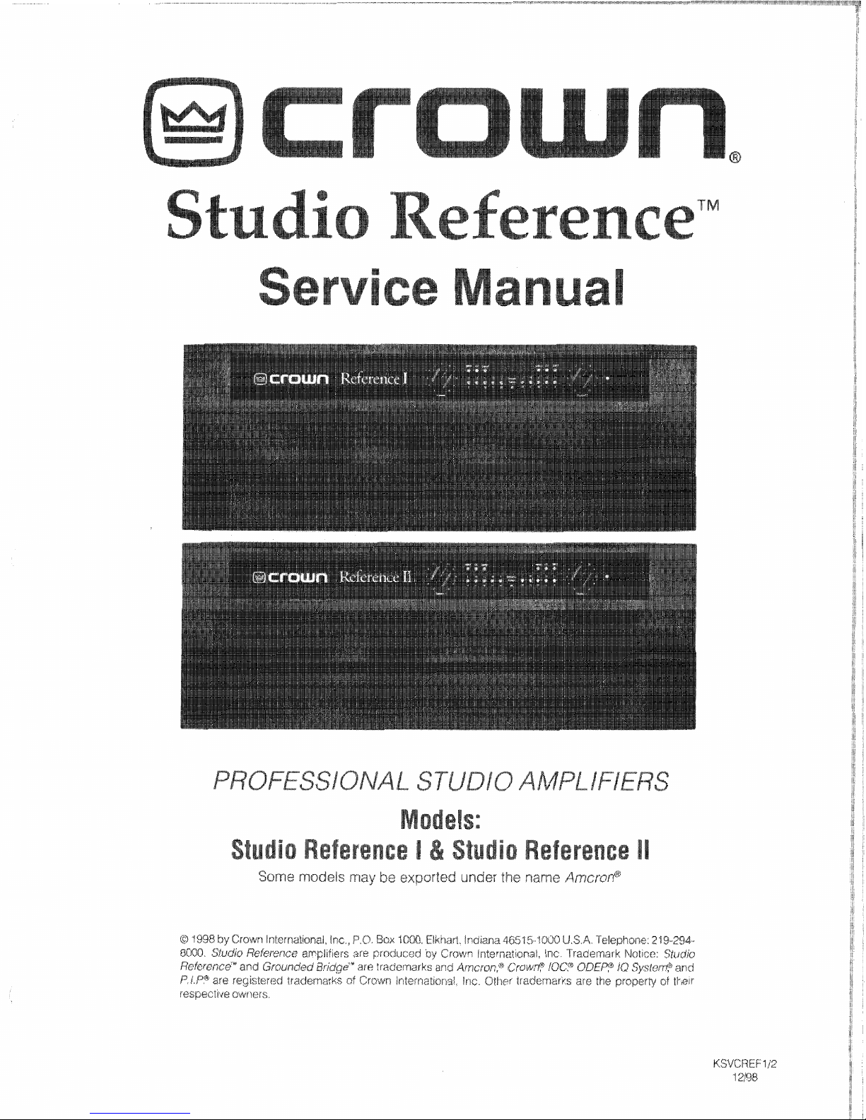
Crown Studio Reference I Studio Reference II, Studio Reference I, Studio Reference II Service Manual
PROFESSIONAL
STUDlO
AMPLIFIERS
Studio
Referenc
dio
Referenee
Some
models
may
be
exported under
the
name
Asrr@rou@
O
"99
8by
Crown
Ir~ternatit:,nal,
fnc.,
P.O.
Box
t
COO,
Elkhart.
lndizn~i
46575-?OQO
U.S.A.
Telephone:
219-244-
8000.
Sfudio
Refere?-9c:c awplifiers
are
produced
by
Crawn
fnterrsaticsnal,
Inc,
xr'radernark
Notice:
Skrdio
Reference'*
and
Gronnd~d
&!.idge7"
are
tradcrnarks
and
Amcnm:'@
&IrcswsT
10C?
ODEP
IQ
S,ysl'cm.e"
and
&"i.PF
are
registered
trademarks
trf
Crcwn
BntsrnationaY,
Irx.
Blher
trademarks
are
the
properv
of
their
respeclive
owrwrs.
@Krawn"
--,,,
Stlidio
Refgrence
Service
Manual
, , ,
.-.
-""...""
R~K
6
*-....-
The
information
furnished
in
this
manual
does
not
Include
all
of
the
de"iaifs
sf
design,
production,
or
variations
of
the
equipment.
Nor
does
it
cover
every
possible
8itua"ii~n
which
may
ariss
during
installation,
operation
sr
maintenance.
if
you
need
special
assistance
beyond
the scope
of
this
manuas,
please
eontact
the
Crown
Technical
Suppart
Group,
Mai/:
P.0.
BQX
4008
Elkhart
lN
465?5-1000
Sbippin-ag:
Pit.
2
S,W,,
171
8
W,
Mishawaka
Rd.,
Elkhark
EN
4651
7
Phone:
$800)
342-6939/(2
1
9)
294-8206
FAX:
$2
"19)
294-8361
Web:
~w~cPQw~~u~~~~co~
TO
PREVEMT
ELECTRlC
SMOCK
80
NQT
REMOVE
TOP
OR
BQnDM
COMERS.
NQ
USER SERVICWBLE
.
PARTS INSIDE,
REFER
SERVOCtNC
TO
QUALIFIED
SERVICE
PERSOMNEL*
DISCONNECT
POWER
CORD
BEFORE
REMOVING
RmR
ENPUT
MODULE
TO
ACCESS
GAIN
SWITCH,
A
PR~VENIR
LE
CHOG
~LECTRIOUE
N'ENLEVU
PA8
LES
CQUVERTURES,
RlEM
DES
PART
lES
UTlLES A L"INT~RIEUR,
D~BRANCHER
u
BORNE
AVANT
DWUVRIR
U
MODULE
EN
ARRI~RE.
f
0
REDUCE
THE
RISK
OF
ELECTRIC
SHOCK,
DO
NOT
EXPOSE
THlS
EQUIPMENT
TO
RAIN
OR
MOISTURE!

Rev.
Q
12-98
Initial Printing

This
page
intentionally
left
blank
Rev
8
-
.
.-
Studio
Reference
Service
Manu3l
@crown
1
Bntroductisn
...................................................................................................
3-1
........................................................................
1.
1
The
Stndis
Referents
1-1
1.2
Scope
................................................................................................
1-1
............................
1.3
Warranty
.~.~~~~~...~.~..A~~~~~....,.........
1-1
2
Specifications
................................................................................................
-2-1
2 . "Berformance
...................................................................................... 2.
1
2.2
Pswei
.................................................................................................
2-1
23
Cantrofs
.............................................................................................
2-2
2.
4
f
ndicators
..........................................................................................
2.2
......................................................................................
2.5
l~putsautput
2-3
2.6
Output
Signal
.....................................................................................
2-3
22
Protcctisn
..........................................................................................
2.3
2.8
Construction
......................................................................................
2.3
3
Va1tags
Conversion
........................................................................................
3-1
.................................................................................................
4
Circuit
Theory
4-4
...........................................................................................
4.1
Overview
4-1
4.2
Features
.............................................................................................
4-2
4.3
Frant
End
Operation
..........................................................................
4-2
4.3.1
Balanced
Gnin
Stage
(BGS)
.....................................................
4-2
4.3.2
Variable
Gain
Stage
(VGS)
........................................................
4-2
4.3.3
Error
Amp
..................................................................................
4.2
4. 4
Voltage
Amplification
.........................................................................
4-2
4.4.1
Voltage
Transfators
....................................................................
4.3
..................................................
4.4.2
bast
Voltage
Amplifiers
(LVAS)
4-3
...............................................................
4.5
Grounded
Bridge
Topology
4-4
.........................................................................
4.5.
Wigh
Side
(HS)
-4-4
4.5.2
Law
Side
(LS)
............................................................................
4.4
....................................
4.6
Output
Device
Emulation
Prccalectian
(OBEP)
4-5
4.7
Ganliol
Circuitry
................................................................................
4-6
4.7.1
DC$LF
Protect
............................................................................
4-6
4.
7.2
fault
Circuit
...............................................................................
4-6
4.7.3
Turn
On
Belay
...........................................................................
4-6
................................................................................
4.7. 4 Fan
Corjtrol
4-6
4.8
Power
Supply
....................................................................................
4-6
4.8.
1
AC
kine
Fiiter
............................................................................
4-6
423.2
Soft
Start
...................................................................................
4-6
4.8. 3 Over
Voltage
Protection
............................................................
4-7
..............................................................................
4.9
Display
Circuitry
"4-7
............................................................................................
4.9.1
1QC
4-7
4"9+2
ODEP
........................................................................................
4.7
........................................................................
433
Signal
Indicafis~s
4.7
.......
...........................................................................................................
"
5
Electrical Checkout
and
Adjustment
Procedures
,,,
.......................................
5-1
51
General
Informatiow
...........................................................................
5-1
52
Standard
Initiat
Conditions
................................................................
5-1
53
DC
Offset
..........................................................................................
5-1
5.4
Output
Bias
Adjustmen$
....................................................................
5-1
55
OBEP
Voltage
Adjustment
.................................................................
5-1
5.6
AC
Pawer
Draw
.................................................................................
5-1
5.7
High
tine
Gutsue
................................................................................
5-1
5-8
Common
Mode
Wejects'sn
..................................................................
5-1
5.9
Voltage
Gain
......................................................................................
5-2
533
Level
Controls
.................................................................................
5-2
5.
1
1
Current
bimi
"r
....
...............................................................................
5-2
512
Slew
Rate
and
*a
OK
Square
Wave
....................................................
5-2
.
..........*<."...........................................................................
5
f
3
Crosstalk
5-3
5.
1-4
Output
Power
...................................................................................
5-9
5.1
5
Reactive Loads
................................................................................
5-3
5.
16
ODEP
Limiting
.................................................................................
5-4
5%
17
Mute
and
Turn-On
Delay
..................................................................
5-4
5.
18
Law
Frequency
Protection
...............................................................
5-4
5.
19
Signal
to
Noise
Ratia
.......................................................................
545
5.20
Intermadulation
Diskoflion
...............................................................
5-5
5.21
LED
Functions
.................................................................................
5-5
5.22
Display
Set-Up
................................................................................
5-5
5.23
Turn-On
Transients
...........................................................................
5-5
5.24
Turn-OM
Transiep-rts
..........................................................................
5-5
525
Past
Testing
.....................................................................................
5-5
6
Schematics
....................................................................................................
6-1
7
Parts
Information
............................................................................................
7-1
7.
1
General
lnfarmation
...........................................................................
7-1
7.2
Standard
and
Special
Parts
...............................................................
7-1
7.3
Ordering
Parts
...................................................................................
7-1
........................................................
....................
7.4
Shipment
.....,.
7-1
7.5
Terms
.................................................................................................
7-7
..
7.6
Illustrated
Parts
List
.......................
.,
,.,,
................................
7-1
.........................
...................
Figure
7.1
Front
Panel
Exploded
View
,..
7-2
......................................
Figure
7.2
Top
Main
Assembly
Exploded
View
7-4
Figure
7.3
Bottom
Main
Assembly
Exploded
View
................................
7-6
Figure
7.
4
Back
Pans[
Assembly
Exploded
View
.......
.,
........................
7-8
Fi%jure
7.5
Output
Assembly
Exploded
View
.......................................
3-1
61
Figt,i
re
7%
Capacitor
Assembly
Exploded
View
...................................
7-12?
Figure
7.
7
PIP
Cage
Assembly
Exploded
View
...................................
7-15
R@K
0
.
-..,
_____ylll~1~1111__
.
, ,
Stvd8"~
Reference
Service
Manuai
@CrQWne
P,
,,
P
.................................................
8
Module
information
........................................................................................
8-4
8.1
General
information
...........................................................................
8-4
8.2
Studia
Reference
1
Module
lnfsrmatisn
.............................................
8-1
............................................
8.3
Studio
Reference
If
Module
Infsrmatisn
8-1
8-4
Q.4397
1-6
Main
Module
........................
...
..
,
..................................
$3-2
85
Q43369-0
Outp&r"lodeelie
..................................................................
8-8
8.6
Q43183A3
Control
Module
..............................................................
8-11
8.7
Q43.450-8
Control
Module
...............................................................
8-14
8.8
843584-2
Control
Module
...............................................................
8-17
8.9
a4301
8-3
Display
Modu8e
...............................................................
8-20
8.1
Q
64331
1-2
Main
Module
.................................................................
8-23
.............
8.1
1
Q43388-0
Main
Module
...................
....
..,,..
,.,
8-28
8.
t
2
Q43389-8
Butput Module
..............................................................
8-33
8.13
a4331
2-0
Display
Module
.............................................................
8-36
@crowne
P
-.."..
.......-
, , , ,
Studio
Reference
Service
pw
Manusf
R~K
0
P
P
Figure
2.1
Studio
Wefsrence
Dimensions
.........................................................
2-3
Figuss
3.1
Specific
Voltage
Wiring
...................................................................
3-1
Figure
32
Circuit
Breaker Selection
......
.............,...
......................................
3-11
Figure
4
.
t
Simplified
Studio
Refereilea
Biock
Diagram
...................................
4-1
Figure
4.2
Simplified
Ampiitier
Front
End
and
Voltage
Ampiifiication
Stages
..
4-3
Figure
43
Simpfified
Grounded
Bridge
...................
,.....
..............................
4-5
Figure
5.
1
Differentiatar
Circuit
........................................................................
5-2
figure
5-2
Differentiated
Square
Wave
..............................
..,,,,..*+.+'.........
5-2
................................................
Figure
53
10
kHz
Square
Wave
...................
...
5-2
Figure
5.
4
inductive
Load
CoId
........................................................................
5-3
Figure
5.
5
5~nd~etive
Load
Warm
......................................................................
5-3
Figure
56
Tartup@
Yest
Waveform
.....................................................................
5-4
Figure
5-4
OBEP
Limiting
Waveform
.....................................................................
5-4
Figure
7.
1
Front
Panel
Parts
.............................................................................
7-2
Figure
4.
2 Top
Main
Assembly
Parts
................................................................
7-4
Figure
7.3
Bottom
Main
Assembly
Parts
.......................
..................................
7-6
........................
....................
Figure
7.
4
Back
Panel
Assembly
Parts
.........
7-8
...................
........................................
Figure
75
Output
Assembly
Par&
,.
7-16
Figure
73
Capacitor
Asssmbly
Parts
............................................................
F.12
Figure
72
PIP
Cage Assembly Parts
.............................................................
7-14
Figure
8.
1
a43371
-6
Main
Msdule
Map
..........................................................
8-7
Figure
8.2
Q43363-8
Output
Module
Map
.....................................................
8-18
Figure
823
Q43383A3
Control
Maduis
Map
....................................................
8-13
Figure
8.4
Q843458-8
Control
Madula
Map
.....................................................
8-16
Figuse
825
Q4J5Q4-2
Control
Module
Map
.....................................................
8-19
Figuw
8. 6 64381
8-3
Bispray
Module
Map
.....................................................
8-22
Figure 8.7
a4336
1-2
Main
Module
Mag
....................
......
..............................
8-27
figure
8.8
843388-0
Main
Module
Map
........................................................
8-32
Figure 83
043389-8
Output
Modube
Map
.....................................................
8-35
Figurs
8'16
Q43312-0
Display
Msduls
Map
..................................................
8-38
t
.I
Ths
Studia
Referenee
The
Studio
Reference
amplifiers
are
the
flagship
sf
Crown
Internatfsna\.
They oRsr
the
best
in
sound
re-
production
with
a
dynamic
range
capable
of
accurately
reproducing
20-bit
digital
recardings.
Super
low
har-
monic
and
intermodulation
dis$or$ion
provides
the
best
transfer
function in
the
business.
And
the
ultra-high
damping
factor
af
20,000
detivsrs
superior
foud-
speaker
motion
control
for
a
tight
and
clean
low-end.
1.2
Scape
This
massr_eaI
contains
sewice
information
for
the
Grown
Studio
Reference
power
amplifiers..
It
ia
designed
I~P
be used
with
the
appilcable
Reference
Manual'
How-
ever,
some
important
information
is
duplicated
in
this
Servica
Manual
in
case
the
Reference
Manual
is
not
readily
availabls.
This
Service
Manual
includes
severaB
sections,
These
sectiians
include
Sp~cifications,
Vottag~
Conversion,
Circuit
Thssry?
EEfectrieal
Che~kout,
Parts
Information,
Module
Information,
aod
Exploded
View
Drawings,
Schematics
are
included.
Note
that
a
Mexdu%e
is
com-
prised
a$
the
circuit
board
with
the
component
parts
instal!@d.
Crown
does
not
sell
blank
(unpopulated)
cis=.
cuiQ
boards.
CAUTIOH:
TRs
infermatien
in
this
manual
Is
Intsndsd
to
b~
ossd
by
an
exparlenc%d
t@~hnlclaa
only
h
1.3
Warranty
Each
Reference
Manual
contains
basic
pslieies
as
re-
fated
to
%he
customer.
In
addition,
it
should
be
staked
that
this
ssrviee
dacumentalisn
is
meant
ts
be
used
snl
y
by
properly
trained
service
personnel.
Because
most
Crawn
products
carry
a
3
Year
Full
Warranty
(in-
ciud~ng
round
trip
shipping
within
the
United
States),
aft
warranty
service
should
be
referred
to
the
Crown
Factory
or
Authorized
Warran&
Sewice
Center.
See
the
applicabls Owner's
Manual
for
warranty
details,
To
find
the
iocation
QI
the
nEarsst
Authorired
Sarvice
Center,
or
to
obtain
instructions
fcar
receiving
Crown
Factory
Service,
piease
contact
tho
Crown
Technical
Support
Group
(within
North
Amerrca)
or
your
Crown/Amcrg;bn
Importgr
(outside
North
America),
Plant 2 S.W,
171
8
W.
Mishawaka
Bd,
Elkhaa,
IN
USA
4651
'7
Phone:
(21
9) 294-8200
Tall
Free:
(8QO)
M2-6939
FM:
(21
9)
294-8301
Web:
.er~wnaudis~com
Introduction
t
-7

Sf
~dio
Reference
Service
Manual
This
pa@@
intentionally
left
blank
introduction
4
-2
Studio
Referenee
Service
,Msnual
The
following
specifications
on
Bode
Wajsctlon
[CMR):
Better
than
100
dB
be-
Mode,
with
an
8
Ohm
load,
a
ted
full
bandwidth
power
from
20
Hz
to
480
Hz,
26dB,
banless
stherwise
specified.
rising
tinearly
Is
better
than
79
dB
at
20
kb4z,
Low-.DJ&o~P@@
t
kHz
Psaar:
Refers
to
maximum
aver-
age
power
in
watts
at
1
kHz
with
0.02%
THO
and
noise..
Sta~d~rB
1
kHz
Power:
Refers
ts
maximum
avsrage
pswer
in
watts
at
I
kHz
with
8.1 % TkJD
and
noise,
Full
B~nd~idth
Pawer;
Refers
to
maximum
average
pawer
in
watts
from
20
Hm
to
26
kHz
with
0.1%
THB
and
noise.
2,l
PeHormsnee
Ftgquency
Response::
~8,MdB
from
20
Hs
to
20
kHz
at
1
watt.
Phase
R~$pon%@:
+5
to
-75
degrees
from
20
Hz
ta
26
kHz
at
3
w~tt~
8ignai-to-noise:
(A-weighted)
reater
than
120
dB
belaw
rcater
than
1
3
7
dB
below
full
bandwidth
powerh
Tat@!
Harmonic
Dldsalon
(TWO):
Less
than
0,02%
a4
rated
low-distortion
I
kHz
pswer.
Less
than
0.1%
af
rated
full
bandwidth
power,
lntsrmoduEIaZlon
Qiatagian
{IMDf:
(60
Ha
& 7 kklz
4:
2)
Studio
R~f~rw
Less
than
0,005%
from full
--*
bandwidth
power
to
78
watts
rising
linearly
to
8.025%
at
78
milfl~atks~
Studio
Ref-
Less
than
0.005%
from
;Bull
bandwidth
power
ta
36
watts
rising
lineariy
$a
0.025%
at
36
mtliiwatts,
Damping
Factar:
Greater
than
20,000
from
"B
BHZ
to
280
Hz,
and
greater
than
2,568
at
1
kHz.
Crosstalk:
(At
rated
full
bandwidth
power,)
Sb~di~
Refer-
Batter
than
106
dB
from
245
Hz
ta
100
Hz,
falling
linearly
to
better
than
70
dB
at
20
kHz,
Betdef
khan
180
dB
from
20
ME
to
f
66
Hz,
falling
tinearly
to
better
than
65
dB
at
20
kHz,
Voltage
G~in::
(With
Isvel
controls
set
far
maximum
ocnt-
put,)
At
the
26
dB
garn
setting,
2Q:h3%
or
26
dB
~0~25
dB,
Studio
m,n,&z;eL
At
0.775
volt
sensitivity?
'I
63:
1
k
12%
or
40
dB
.-
1
dB;
at
1.4
volt
sensitfvity,
57:
1 k 12%
or
35
dB
k
1
dB.
Studio-
At
0.775
volt
sen%itiviby,
-
..-.
69:kj
2%
aor
37
dB
41
dB;
at
"84
volt
sensitivity,
38.1
~12%or32dB~1
dB.
2,2
pa we^
Ps~er
Bandwidth:
(At
standard
1
kHz
power.)
&,df-rence6:
-^B
dB
from 5 Mz
to
27.5
kHz
and
-3
dB
from
3
Hz
ta
32.8
kHz.
-1
dB
from
5
Hz
fa
28.6
kHz
and
--3
dB
from
2.3
Hz
to
34.4
kHz,
tsw-Di%tofllsn
f
kHz
Butput
Power:
Sf
udio
....
Rcf@rea&
$t~?rea
Made
with
both
cchannsbs
driven.
1,160
watts
per
channel
into
4
ohms,
768
watts
per
channel
into
8
ohms.
B~idge-Mono
mode:
2,228
watts
Into
8
ohms,
1,580
watts
into
16
ohms
P8~3I/e/-Msn0
mode:
2,37
5
watts
into
2
ohms,
1,565
watts
into 4 ohms.
m,,B@-
Stereo Mode
with
both
chag.gne!s
driven:
555
watts
per channel
into
4
ohms,
355
watts
per
chanilel
into
8
ohms.
Bridge-Mono
mods:
"i
1
10
watts
into
8
ohms.
71
5
watts
into
16 ohms.
Parab/e/*!dons
n~ade:
1,115
watts
into
2
alms.
730
watts
inta
4
ohms,
Enable:
A
front
panel
push
button
used
to
turn
the
Stereo
mode
wid)~
both
~haanneIs
driven:
amplifier
on
and
off,
1,190
watts
per
channel
into
4
ohms.
800
watts
per
chaunef
iota
8
ohms,
Level:
A
front
panel
rotary
potentiometer
far
each
ehan-
nel
with
3
1
dstents,
used
$0
CB~~FOI
the
output
level.
Bridge-Mono
mode:
2,375
watts
inis
8
ohms.
Stsreomono:
A
three-pasitiaw back
panel
switch
used
1,595
watts
into
1
6
ohms.
to
select
either
Stereo,
Bridge-Mano
or
Parallel-Msns
Par~jIef-Mono
mode:
2,350
watts
into
2
ohms,
SsnsitivlQ:
A
three-position
switch
inside
the
P,l,I,p
corn-
1,588
watts
into 4 ohms.
partment
used
ta
select
the
input
sensitivity
for
both
ek?annefs:
6,795
ai
1.4
volts
for
standard
'I
kHz
pg;aw~r,
St~d8"o Refefcnce
H:
or
26
dB
voltage
gain,
S!W@Q
mode
wifh
both
cchanne/s
drjven:
565
waus
pea
channel
into
4
ohms.
Mater
OnfBff:
A
tws-position
switch
behind
the
front
360
watts
per
channel
into
8
ohms.
pane!
used
to
turn
the
front
panel
meters
on
or
off,
Bridge-Mono
m~d~r
3, f 45
waEs
into
8
ohms,
720
wakk
into
16
ohms
Par8$/@/-Mono
mode:
7,135
watts
into
2
ohms.
"715
waE%
into
4
ohms,
Meter
Display
Mode:
A
twa-position
switch
behind
the
frsnt
panel
used
to
set
the
display
mudc
tor
ths
front
panel
meters.
Display modes
include
dynamic
range
af
the
output
signal
in
dB
or output
levels
in
dB.
Ground
Lift:
A
two-position
back
panel
switch
used
to
isslate the
irrput
phone
jack
and
AC
{chassis)
grounds.
Full
Bawdwidth
Butput
Pewer:
(20
Hr
lo
28
kHz)
Reset:
A
two-p~~ltion
back
panel
switch
used
fa
roset
the
AC
mains
circuit
b~eaker*
E@r@o
made
wjtfi
both
-lh~aanne/s
drivepa:
1,075
watts
per
chanaal
into
4
ohms.
2,4
lndicatars
768
watts
per
chaalnel
ir3Po
8
ohms.
Enable:
This
indicator
shows
the
on/M
status
of
the
unit's
How-voltage
power
supply
BrBdge-M~f?~
2,150
watts
into
8
ohms+
"3,535
watts
into
f
6
ohms.
$&2dio
Ref-K
St~f-sa
mode
wifk
bath
chhanng!~
db^ven:
495
watts
per
channel
into 4 ohms.
340
watts
per
chaanel
into
8 ohms.
Brid~e-Mgbf?~
mode:
1,020
watts
into 8
ohms.
698
watts into
16
ohms.
Load
Impedsn~e:
Safe
with
all
types
of
loads,
Raked
far
4
ts
8
ohms
in
stereo
mode,
8
ts
16
ohms
in
Bridge-
Mona made,
and
2
to
4.
ohms
in
ParalteI-Mon~
MO~G,
Required
AC
Mains:
56
or
60
Hz;
106,
120,
200,
220
or
240
VA6
(k
10%)<
Both
units
draw
90
watts
or
less
at
idle.
Signal::
Each
channel
has a signal inclicatar
that
flashes
to
show
audio
output.
i@C:
Each
channel
has
an
18C
indicator
%hat
flashes
if
the
output
waveform
differs
from
the
input
wavsform
by
0.85%
or
more.
The
LED$
act
as
sensitive
distsr-
tion
indicators
to provide
proof
of
di~f~rtian-free
per-
formance,
In
Paralfel-Mono
mode
the
channel
2
/0@
Ilght
stays
an.
0DEP:Each
channel
has
an
ODEPindieator that
shows
the channel's
resewe
energy
status,
Normally,
the
LEDs
are
brigfatly
tit
to
show
that
reserva
energy
is
available.
In
the
rare
event
that
a
channel
has
no
re-
serve,
its
indicator
wisi
dim
in
proportion
to
BDEPlim-
Dynamic
Ranga/Lsuel
Meter:
Each
Channel
has
a
five-
segment
meter that
displays
either
the
dynamic
range
of
the
output
sigrrai
in
dB
sr
the
output
love!
in
dB,
(From
the
factory, the
amplifier
is
set
to
display
dy-
namic
range.)
As
dynamic
range
meters,
they
show
%he
ratio
sf
peak
to
average
power
of
tach
channel,
As
output
level
meters
they
show
how
high
the
~~~lput
levels
are
relative to
standard
1
kHz
powerq
2.5
llnputlOutput
input
Csnneetor:
Two
balanced
'!,is-inch
jacks
an
the
back
panel
and
two
balanced
three-pin
XLR
connec-
tors
on
the factory-installed
P..B,?-FX,
lnput
impsdanee:
Nominally
10
K
ohms,
balanced
Pdornina!ly
5
K
ohms,
unbaianced.
I~put
San%itiuiQ:
Settings
include
0,775
volts
sr
1
A
volts
for
standard
1
kHz
pswea: or
26
dB
voleage
gain.
Output
Canaeetam:
Two
sets
of
color-coded
5-way
bind-
ing
posts
far
each
cha~3rrel
(for
connecting
barlana
plugs,
spads
lugs
si
bare
wire),
Qutput
Impsdaase::
Less
than
10
miBliahms
in
sarisa
with
2,s
micr~henries,
DC
Output
8@ssZ;
(Shorted
input)
32
millivslts.
2.6
Output
Signal
Starsa:
Unbalanced,
twa-channel.
Brldgs-Mona:
Balanced,
singla-channel.
Channel
f
controis
are active;
channel 2 should
be
turned
down.
Parallai-Mono:
Unbalanced,
single-channel.
Channel
"icontmls
are
active;
channel
2
is
bypassed.
2,7
Protection
ODEP:
ff
unreasonable
operating
conditions
$~~g;;ur
which
could
stress
the
output circuitry?
the
QDEPcir-
Input:
Input
overload
prstectisn
is
furnished
at
the
amplifier
input
to
limit
current.
Turn
On:
The
four
second
~C~TM-Q~
deilay
prevents
dam
gerous
turn-on
transier~ts,
2,8
Constrvctlon
Steel
chassis
with
durable
b8ack
finish,
aluminum
front
panel
with
super-glass
Imron
finish,
lexa~,
averiay?
and
a
specially
designed
flaw-through
ventilation
system
from
front
to
side
panels.
CoeiJng:
Convection
cooling
with
assistance
from
the
computerized, on-demand
proportional
cooling
fan.
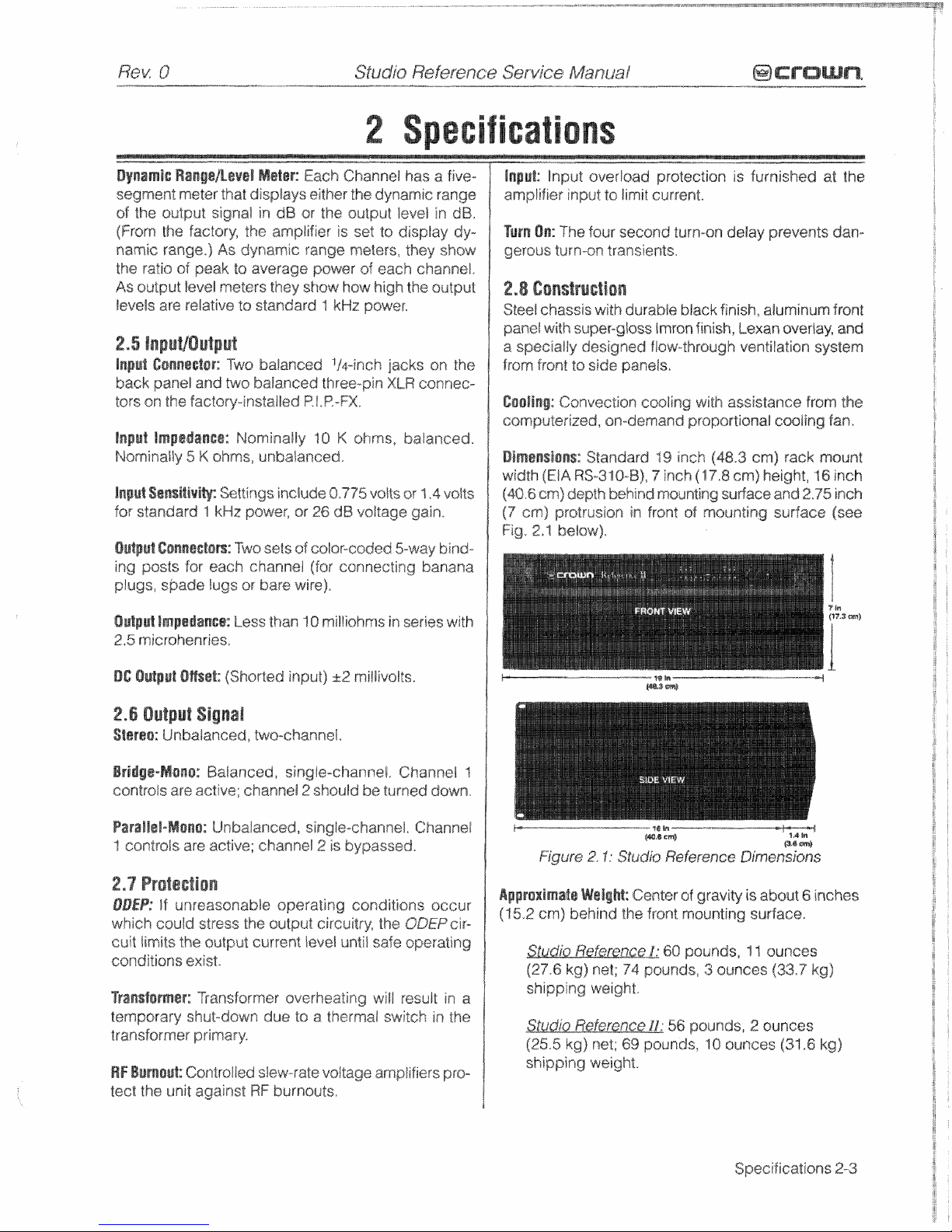
Dimen$ions:
Standard
19
inch
(48.3
em)
rack
mount
width
fElA
RS-316-B),
9
inch
(17.8
cm)
height,
16
inch
(40'6
CM)
depth
behind
mounting
surface
and
2.75
inch
(7
em)
prstrusion
in
front
sf
mounting
surface
(sea
Fig.
2.1
belaw),
Apprsxlmata
WaiigM:
Center
of
gravity
is
about
6
inches
(15.2
cm)
behind
the
front
mounting
surface.
cuit
limits
the
output
current
level
until
safe
operating
conditions
exist.
60
pounds,
11
ounces
unds,
3
ounces
(332
kg)
shipping
weight.
Trensformer:
Transformer
overheating
will
result
in
a
1
temporary
shut-down
due
ta
a
ttmerrnal
~wifch
in
the
transformer primary-
RF
Burnout:
Controlled
slew-rate
voltage
amplifiers
pro-
tect
the
unit
agairlst
RF
burnouts,
56
pounds,
2
ounces
(25.5
kg)
net;
69
pounds,
"1
0ouncss
(31
"6
kg)
shipping
weight.
Specifications
2-3

Studio
Reference
Service
ManuaI
This
page
inten&ianally
/aft
blank
Studio
Reference
Service
Manual
age
Convers
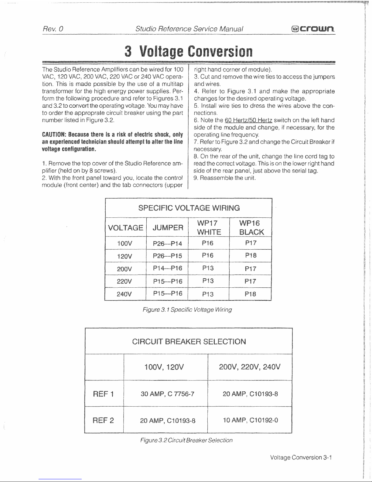
The
Studis
Reference
Ampfifiers
can
be
wired
for
100
VAC?
I20
VAG,
200
VAC,
220
VAC
or
240
VAC
opera-
tion,
This
is
made
passible
by
the
use
of
a
multitap
transformer
for
the
high
energy
power
supplies.
Per-
form the
fallowing
pracedure
and
refer
%s
Figures
3.3
and
3.2
ta
convert
the
operating
voltage.
YOU
may
have
to
order
the
approprate
circuit
breaker
using
the part
number
listed
in
Figure
3.2.
CAUPfO#:
B~eausa
thare
1%
a
risk
of
slsctr!~
sheek,
sniy
on
gxperisne~d
t~ehnician
ahould
aggmpfk
ts
altgr
the
line
valtage
contlguratiian,
1.
Remove
tha
tap
cover
of
the
Studio
Referenee
am-
plifier
(held
on
by
8
screws).
2,
With
the
front
panel
toward
you,
locate
tka
controt
module
{front
center)
and
the
tab
connectors
(upper
-
-".-
right
hand
corner
of
module).
3,
Cut
and
remsve
the
wire
ties
to
access
the
jumpers
and
wires,
4.
Refer
to
Figure
3,1
and
make
the
appropriate
charrges
for
the
desired
operating
voltage.
5.
lnstaBI
wire
ties
to
dress
the
wires
above
the
con-
nections.
6,
Note
the
switch
on
the
ief2
hand
side
of
the
module
and
change,
if
necessary,
for
the
operating
line
frequency.
7,
Refer
"I
Figure
32
and
change
the
Circuit
Breaker
if
necessary+
8.
On
the
rear
05
$he
unit,
change
?$"re
line
cord
tag
to
read
the
correct
valtage.
This
is
on
the
lower
right
hand
side
of
the
rear
panel,
just
above
the
serial
tag.
9,
ReassembHe
the
unit.
WPt
6
VOCrAGE
JUMPER
1
Figure
3.1
Specific
Vo1tage
Wifing
Ct
RCUfT
BREAKER
SELECTiON
30
AMP,
C
7756-7
1
20
AMP.
Cl
01
93-8

@
crawma
--.,."---
. , .
, " '
Studio
Reference
Service
Manuaf
-."...--,
.
R@K
0
This
page
intentionally
left
blank
Voltage
Conversion
3-2
Studio
Reference
Service
Manual
INVERTING
LOW
SIDE
BRIDGE
OUTPUT
BWUNCE
PNP
STAGE
Circuit
Theory
4-1
Bcrcrurn.
, , ,
Sfudjo Weference
Service
Manual
--,-..-.-
-.".-
..,.
".,-
R~K
0
-
k
to interrupt around
lw~=os
via
the
Ground
"
-
Studio
Referenee amplifiers utilize numerous
Crown
Lift
Switch.
The
non-inverting
(hot)
si&
of
the balanced
innovations, including gf@tuflded
bridge
and
ODEP
input
is
fed
to
the
non-hverting
input
of
the;
firs@
op-
teehnofogies.
Cooling
t~chniques
make
use
of
what
is
amp stage. The
inver"ring
(negative)
side
of the
bal-
essentially air conditianer technology.
Air
flows
bottom
ancsd input
is
fed
to
the
inverting
input
of
the
firswsp-
lo
top, and front to
side.
Air
ftsws a shafi
distance
amp stags. A potentiometer
is
provided
far
esmmon
across
a
wid@
heatsink.
This
type
of air flow pro.\rides
mod@
rejection adjnmstment
(R5f
2).
Electricaiiys the
BGS
significantly better emling than
the
"wind
$unnel'"tech-
is
at
unity
gain, (From an
audio
perspe~tive, however,
nology
used
by
many other manufacturers, Output
this
stage
actually provides
+6dB
gain
if
a
fully
bai-
transistors are
of
the
metal can
type,
rather
than
fh~
anced signal is
placsd
on
its
iraput.)
Tho
BGS
is
a
nsn-
plastic case
style.
This
alIo\~s
for
a significantly higher
thermal
margin
for
the given voltage
and
current rat-
ings.
Ail
devices
used
are tested
and
grad~d to en-
sure
maximum
reliability, Another electronic
technique
used
is
negative feedback. Almost
atl
power amplifi-
$put
sf
the
BGS,
the signal goes to
the
ers utilize n~gativa;. feedback
80
control
gain
and pro-
gain
is
determined
by
the
position
of the
vide
stabifity$
but
Crown
uses
multiple
nested
feed-
itch,
and
lev@/
is
detc~mined
by
the
level
back
imps
far
maximum
stability
and
greatly
impag>k/ed
s
an inverting stage
with
the
input
being
damping.
Studio Reference ampiifiers
have
damping
mp
stage. Because
gain
after this
stage
in
@XC$S$
af
20,000
in
the bass frequency range.
This
B
(factor
sf
2Q),
greater amplifier sensi-
feedback,
along
with
our compensation and
ut"l3-l~~
sd
$y
csntrosling the
ratio
of f~edback
distortion output tapol~gy~
make
Grown Studio
Ref-
nee,
The Sensitivity Switch sets the
in-
erence
amplifier superior*
put impedance to this stage
and
varies
the
gain such
that
the
overall
amplifier gain
is
26
dB,
or
is
adjusted
Fsatt~res
specific
to
the
Studio Reference
include:
A
or
0.775V
ar
d.4V
input
to
attain rated
high
power
toroidal Esansfsrmsr; Computer controlad,
varjable
speed,
whisper quiet
fan;
Built
in
AC
power
fiffes;
Soft
start
circuit
Za control inrush curroot;
Fuji
ov-
ervodtage and internal fault protection,
This
ampli-
tpuX
from
the
VGS
is
fed
to
the non-
fier can operate
in either
Bridgge;! or Parallel Mans mode,
the
Errof
Amp
op-amp
stage through
as
well
as
in
Dual
(stereo)
made,
A
sensitivity
switch
capacitor
$C
t
00)
and
input
resistor
a)lows seiectian
sf
input voltage
required
for
rated &rut-
output
is
led
back
via
the
negative
put.
Level
cnr-llr~ls are mounted
on
the front panel and
op
re~istor
(W
1Q3),
The
ratlo
of
feed-
are
of
the rotary type, Front
panel
indicators let
the
user
know the status
of
amplifier
enable,
QDEP9
signal
tpuWof
the
amplifier
at
26
dB,
Bi-
presence
(SP!),
and
distortion
(90C),
Alsa
included
on
revent averdriving the Error
Amp.
the
front panel is a five-segmet display Tor each chan-
mp
amplifies the difference
be-
riel
which
displays
either
dynamic
range
tn
dB
ar
aut-
ut
signals,
any
difference
in
the
put
level
in
dB,
two waveforms
will
produce
a near open loop gain
condition which,
in
turn,
results
in
high
peak auWpu&.
For
addiriauai
details s~fer to the specification section,
ths
Error
Amp,
called the Error
or
ta
the appficable WaFerence Manual,
Signal
(ES)
drives the Voltage Translators,
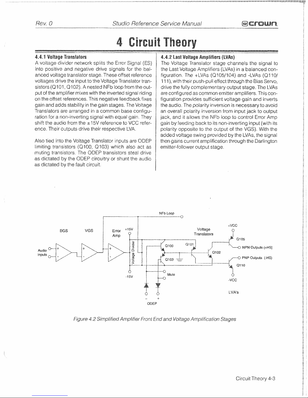
4.3
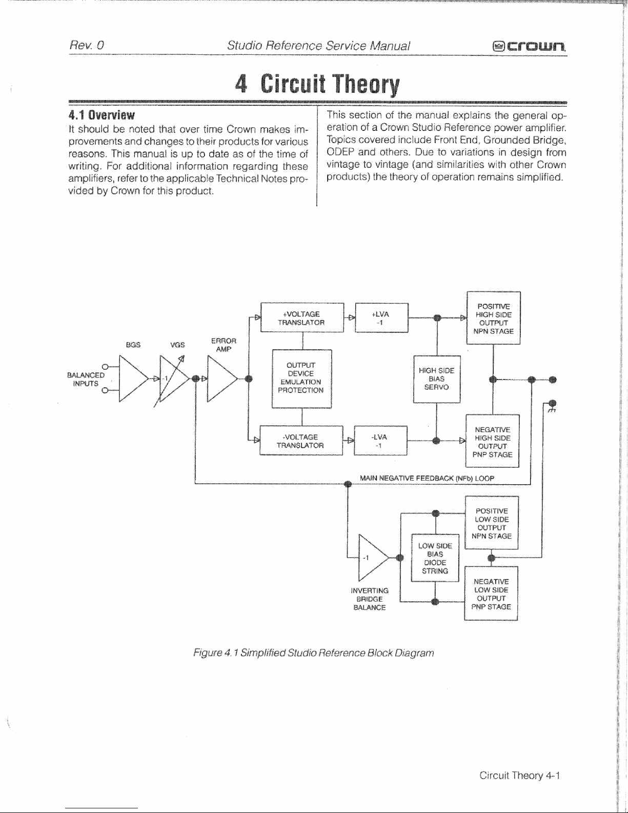
Front
End
Operation
The
front end
is
comprised
of
three
stages:
Balanced
Gain Stage
(BGS),
Variable
Gain
Stage
{VGS),
and
the Error Amp. Figure
42
shows
a
simplified
diagram
of the front
end and
voltage ampixfieation stages,
4-3,f
Balanced
Gain
Stage
(80%)
lnpk~t
ts
the
amplifier
is
balanced, The
shield
from
the
1/4"
inputs
may
be isolated
from
chassis ground
by
4.4
Voltage
Alnplifi~ation
The
Voltage
Translator
stage
separates
the
output
of
the Error
Amp
into
balanced positive and negative
drive
vol"s~ge?s
for
the Last bltage Amplifiers
(LVAS)~
translating the
signal
from ground referenced
n
15V
to
kV@c
referenee,
LVAS
provide the
rnak
voltage ampli-
fication
and
drive
the
High
Side
output stages.
Be-
muse there
is
a
slight
lass
of
gain
in
the
translator
stage,
the
gain
after the translatar
is
a
factor
of
25.2,
Cir~uit Theory
4-2
ence.
Their
outputs
drive
their
respechive
tVA,
muting
transistors,
The
QQEP
transistors
steal
drive
as
dictated
by
th@
BDEP
circuitry
or
shunt
the
audio
as
dietated
by
thg
fault
circuit,
Circuit
Theory
4-3
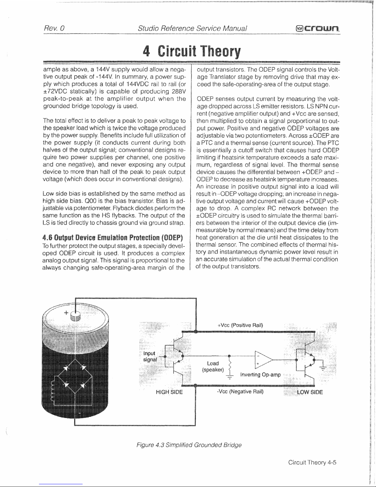
Figure
4.3
is a simplified
exampfe
of
the
grounded
bridgs output topology.
It
consists of
four
quadrants
of
three deep DarDington (composite) emitter-follsw~r
stages per channel: one
NPN
and
one
PNP
an
the
High Side of
the
bridge (driving the
Isad),
and
apse
NPN
and
one
PMP
an
the
Low
Side
of the bridge (con-
trolling
the ground reference for %Re rails).
The
output
stages
are biased
ta operate
class
AB+B
far ultra
low
distortion
in
the signal zero-crossing region and
high
efficiency.
4,5.%
High
Side
[NS)
Thhe
High
Side (HS)
af the bridge operates much like
a
conventional
bipolar push-pull output configuration,
As
the input drive vsitage becomes more po%itive, the
HS
NPN
conducts
and
delivers positive voltage
to
the
10ad,
Eventually
the
NPN
devices reach
full
conduc-
tion
and
+Vcc
is
acrsss the
load,
At
this time the
HS
PNP
is
biased
off.
When
the
drive
signal is negative
going,
"Be
HS
PNP
canducts to deliver -Vcc to the load
and
the
HS
NPN
stage
is
off.
The
output
of
the
+LVA
drjvm the base
of
$8.~
pradriver
device.
Sgsgethar, the predriver
and
driver farm
the
first
two parts
sf
the three-deep Darlington and are
biased
class
AB,
They
provide output drive
through
the
bias
resistorx
bypassing
the
output devicas,
at
Bevels
be-
Isw
about
180mW,
An
RLC
network between
the
predriver and driver
provide
phase
shift
csmpensa-
tion
and
limit driver
base
current
$a
safs Bevels. Output
devices
are biased class
B,
Just
below
s%sculotf.
At about
1QOmW
blr~tpat
they
switch on
to
eonduct
high
current
to
the
load. Together with predriver
and
driver? the out-
put
device provides
an
averall cFass
AB+B
output,
The
negative half
sf
the
HS
is
almsst
identical
to
the
positive half, except that
the
devices are
PNP
One
difference
is
that the
PNP
bias
resistor is
slightly
greater
in
value
sa
that
PNP
output
devices
run
closer
to
the
cutoM
level
under static
(no
signal)
conditions,
This
is
because
PNP
devices require greater drive current.
WS
bias
is
rsgulated
by
Q18,
the
Bias
Seavs,
QlS
is
a
Vbe
multipiier which maintair-rs approximately
3,2V
Vee
under static conditions,
The
positive
and
negative
halves
of
the
WS
output
are
in
parallel
with
this
3.2V
With a full base-emitter on voltage
drop
across
predrivers
and
drivers, tha balance of
voltage
rasuits
in approximately
.3V
drop across
the
bias
resistors in
the positive half,
and
about
.5V
acrsss
The
bias resis-
tor in the negative
half,
Q
J
bn$
~~nd~clior~
{and
thus bias)
A
diode suing pr~vents
excessive
charge
build
up
within the
high
conduction output devices
whew
off,
Flyback
diodes
shunt
bask-EMF
pulses
from
reactive
loads
to
the
power supply to protect output devices
from
dangerous reverse voltage levels. An output
ter-
minating circuit blocks
WF
on
output
lines
from
enter-
ing
the
amplifier
through its output connectors,
4,5,2
L@w
Side
(L8)
The
tow Side
(LS)
operates
quite
differently.
The
power
supply
bridge
rectifier
is not ground referenced, nor
is
the
secondary
of
the main transformer,
in
othsr
wards,
tha
high
vsltage power supply
floats
with respect
ta
ground,
but
~Vcc remain canstant with respect
to
each
other,
This
allows
the pswer
supply
to deliver
+Vcc
and
-Vcc
from
the
same
bridge
rectifier
and
fiitsr
as
a
total difference
io
potential, regardless
of
their voltages
with
respect
ts
ground.
The LS
uses
inverted feed-
back
from
the HS
output
$0
control
the
ground refer*
ence
for
the
rails
(AVCC),
Both
LS
quadrants are ar-
ranged
in
a
three-deep Darlington
and
are
biased
AB+B
in
the
same
manner as
thc
WS,
When
the
amplifisr output swings positive,
the
audio
is
fed to an
sp-amp
stage
where
it
is
inverted,
This
inverted signal is delivered direeIIy to
the
bases
of
the
positive
(NPN)
and
negative
(PNP)
LS
predrrivers.
The
negative drive forces the
LS
PMP
devices on
(NPN
off),
As
the
PNP
devices
coaduct, VCB
af
the
PNP
Darlington drops.
With
LS
dsviics emitters tied
to
ground, -Vcc
is
pulled toward ground reference.
Since
the pswer supply
is
not ground referenced (and the
tatai
vsltage from
aVcc
to
-Vcc
is
constant)
+VGC
is
forced
higher
above
ground potential.
This
continues
until,
at
the
positive
amplifier output peak,
-Vcc
-.
OV
and
+VGC
eq~aIs the total
power
supply potential with
a
positive pslarily'
In
the
Reference
1,
for
example,
%he
power
supply
produces
a
totat
af14488
from rail ts
rail
(k72VDC
me?asur@d
from
ground
with
ns
signal),
therefore,
the
amplifier output can reach a positiva
peak
sf
+"I
44v*
Cosrversely, during a negative swing
af
the
HS
output
where
HS
PNP
devices conduct,
the
op-amp
would
output
a
positive
voltage forcing
hS
NPN
devices
to
canduct.
This
would
result
in
+Vcc
swinging
tsward
ground
potential
and
-Vcc
swinging
further from
groidnd
patentraf.
At
tl-$6
negative
amplifier sutpvt
peak,
SVCC
=z
OV
and
-Vcc
equals
the tstal power supply
potential with
a
negative pofariWy. Using
the
same
ex-
Circuit
Theory
4-4
E
!
t
Rev
0
k
-..,-
,,.
,
Sfudio
Reference
Service
Manual
@CraUme
rn
I
k72VDC
statically)
is
capable
of
produsing
288V
rent (negative
amplifi~r
output)
and
+Vcc
are
sensed,
An
iocrease
in
positive
output
signal
into
a
load
will
measurable
by
normal
means)
and
the
time
delay
from
@crown*
--
Studio
Refer~nce
Service
ManuaE
-..-.-.
-"-
p..-.p
---
, , ,-
R@K
Q
4.7
C@~tr@l
eireuitry
nal.
As
the outpeat transistorlheatsink
increases
in
tem-
The
Reference amplifiers
have
fault protect circuitry
Peratu~e, the
ODEP
voltage
kvei
will
drop fmm
to
guard
against dangerous
DC
voltages
and
turn
on/
+joVBC
f3ear
~~~Cv
If 1s
a
drop
in
one of
off
transients,
At
the
heart
sf
this
~ir~~ifry
the
win-
both
QDEP
vsltages
it
will
Cause
the
fan
csntroi
sig-
dew
comparator
~102,
?kg
fan
control girc~ij:
moni-
nal to change,
The
fan
contra& signal starts
out
around
tors
the
thermal conditions,
via
the
OBEP
eireuit,
and
-12.5VDC,
3rd
after
complete
ODEP
limiting,
ends
regulates
the
fan
speed
accordingly,
up
at
+
1
2,5VDC0
Phis
voltage
is fed
into
the inverting
input
of
the
op-amp
U
1
B,
The initial output
sf
U1
B
is
4.7,1
DCBF
Pr@t@@
high
$+24V),
and
as
the
fan
control
signal
becomes
The
amplifier output sigf-ral
is
passed
through
a
low
more
positive,
this output
will
became
low,
thus
turn-
pass filter
(R184,
C
1
19,
R186
*and
C107)
ts
the
win-
ing
the
fan
accordin~j~~ The output of
U1
I3
drives
dew
comparator
(UJQ21,
if
DC
campsnent ex-
U4,
an
opts-triac,
which
in
turn
drives
Q4,
a
triac
in
ceeds a predetermined level, the output of the
cam-
AG
supply for
fhe
fan,
parator (pins
1
and
2)
goes
law.
The
result
is
U302
pin
23
going
to a high
state
which
turns
on
the
muting
Ph@
Gating
Signadis
fed
into
the
nsn-inverting
input
of
transistors
and
disables
the
high
energy
supply
by
$he
QP-amP
Uj@+
This
gating signal
is
a
p~~duct
of
opening
the
relay
K2.
U7
A,
Q3,
and
the
Fan
Enable
signal
from
the
display
madule.,
C12
and
RE3
farm
an
RC
timing circuit that,
4,7,2
Fsuft
Circuit
from the
+15V
supply,
begins
Is
charge,
U1A
rnoni-
The
fau&
circuitry
is
designed
to
mute
audio
and
tars
the
tine
voltage
wave
farm
and
is
a
Oil
crossing
disa$le the
high
energy
supply
in
the event of
an
out-
detector.
Every
lime the
line
waveform crosses
OV,
Q4
put
fault.
A
fau/$
is
defined
as
any time
in
which
the
is
turned
sa?
and
discharges
C12,
This
causes
a
ramp-
output
semicsnductars,
in
both
the
negative
and
posi-
ing
type
waveform.
The
higher
p~$i$ive
portion
of
.&he
tive
sections, draw excessive currents,
waveform
is
used
to
turn
off
%he
~pto-triac,
aven
when
the
fan
contrkal
signat
itself
is
aF
a value
ks
turn
sn
the
The
[ow
side
of
&ridge
fault detection consists
sf
Q128,
fan.
Therefare, the
fan cantrod curr~nt
has
a
duty
cycle,
Q329
and
Q130,
ff
both
NPN
and
PNP
output devices
are
conducting excessive
cajirrents,
tha
output
af
U'T82
'The
f%f?
Enabje
%nai
cQm@s
from
the
display
!"nod-
(pin
13)
is
forcegs$
high,
This
disables
the
high
energy
u!@
and
holds the
Gating
Si~flaf
high
when
the
amp&
supply
and
mutes
the
audio
path,
fief
is
in
standby<
"I^'herefsfe
the
fan
will
not
turn
when
the amplifier
is
in
standby*
The
high
side
sf
bridge
fault
detection
consists
of
a126,
Qf
27
and
U101.
This
circuit compares the
NPN
and
BNP drive
to the
feedback
signal,
giving
a
repre-
At
the
heart
of
the
power
supply
is
a
muiti-tap torraidaH
sentation
of
output
devics
current.
If
excessive
cur-
power
transformer,
There
are
two ungrounded, high
wnt
occurs,
the window cegmparatsr
U
1
Q2
is
triggered
energy,
secondary
windings,
one
for
each channel,
through the
opto isslatsr
U101.
and
there
is
one
low voltaga winding
for
the
24V
sup-
plies,
"f?er@
is
also
a
thermal
eu%
off
switch
built into
4.1.3
TBFR
8n
Bs%ay
the
transfarmer
wtlich
will
disable the
secondary
wind-
During
power
up,
the
capacitor
C'I
18
is charging,
ings in
the
event
of the transformer overheating.
which
causes %he
nan-inverting
input
{pin
-4
09
of U 182
to
be
!OW
and
the output
(pin
13)
$0
be
high,
With
pin
4,8,1
AC
tin@
Filter
13
high,
the
high
energy
taik
are
disabled by
the
re-
824
and
025
are
ir-t
the
AC
primary,
They
are
wired
lay
K2,
and
the
audio
is
mutsd
by
the muting transis-
such
that they
null
out
any
DC
compo9-ren"in
the
AC
tors.
Aft~r
approximately
4
seconds,
C1
"I
Qis
fully
pawere
This
done
because
the tarriodiat
transformer
charged
and
pin
10
is
pulled
high,
thus
causing
pin
may
develop
a
mechanical
buzz
if
them
is
any
DC
13
to
go
low
and
the
amplifier
to
:,cams
out of
standby-
shift
in
the
AC
waveform
applied
to
the
transfarmer
4,7,4
Fsn
Centre!
The
F8n
ContrdSi~na$is
t.aken
from
the
positive
ODE$
bias
valfages.
Both
channel
1
and
channel
2
ODEP
inrush current that
is
possible
with
the
voltages
are
eambined
to
create
the
fan
c~rrtrsl
sig-
rmer, a SO%$
Start
Circuit
has
been
in-
Circuit
Theov
4-6
and
power
is
applied
diractty
to
the
transformer.
4,9.3
Signal
Indlcatlan
4,8.3
Over
Voltage
Proteetion
Ul
El
serves
as
a
window
comparator
for
the
purpose
of
over line
voltage
cantro!, In the
event that
the
line
vslfags
sxceeds
10%
over
the
rated
line
voltage,
the
high
energy
power
supplies
are
disabled,
W7
%up-
plies
the
regulated
+
I
SV
to
pin
"I
of
U
1
B
and
serves
as
the
window
reference
level.
With
pin
10
in
csntrof
of
U1
D,
&he
output:
(pin
13)
has
a
logic
law
which
is
applied
across
033
and
014,
This
prevents
csndue-
tisn
and
allows
Q1
to
remain
on,
which
thus
allows
K2
to
remain
ensrgired
Resistors
W3,
W4,
R5
and
R6
serve
a$
a
resistor
drop-
ping
neWsrk
from
the
unregulated
+24V
supply
to
ground,
As
the
line
voltage
incraas~s,
the
unregulated
supply
will
increase,
The
voltage
iievsD
sn
the
wiper
of
R4
is
applied
to
Pin
1
1
(non-inverting
input).
When
the
Hevel
exceeds
%he
window
level
of
pin
-10,
the
circuit
switches
states,
This
allows
Dl
3
and
0
14
to
canduet,
incorporated
on
the
display
module are three
modes
ef signal
indication.
SB
(Signal
Presence
Bndicnfiow)
U
1 A and
D3
serve
to
rectify the
amplifier
output
sig-
nal.
U1
B
takes
this
rectified signal
and
drives
the
LED,
E3,
which
illuminates
any
timg
there
is
signal
pre~ent
at
the
autpkdt of
the
amplifier
channel,
Dynamic
Range
With
the
switch
51
in
the
Dynamic
position,
this
recti-
fied
audio
signal
is
placed
on
the
invsrtin~
inputs
of
a
sequence
of
window
comparators.
This
signal
is
recti-
fied
but
unfiltered,
therefore
it
contains
ah@
peak
value
of
%he
audio
waveform,
U3C,
U3D,
USA,
U5B
and
U5B
serve
as
the
current
sources
for
the
five
Dynamic
Range
LEDs.
R29,
R3t
R33,
W35,
R37
and
R39
pro-
vide
a resistor
dropping
network
for
the
inverting
in-
puts
"l
athe
LED
drivers,
placing
a
logic
high
on
the
base
0%
01%
This,
iu
turn,
This
same
reclifisd
signal
is
placed
an
the
non-invert-
biases
off
Q
1
and
de-energizes
K2.
ing
i~lputs
via
the
filtering
Function
of
C3
and
the
op-
amp,
U1
C.
This
filtered
sigr~al
is
of
an
RMS
value,
With
4.9
Display
Circuitry
the
nan-inverting
inputs
receiving
the
RMS
value, and
the
inverting
inputs
receiving
th~
peak
value,
the
aut-
4.9.1
ilOC
pull
of
each
LED
comparator
equals
the
dynamic
U3A
and
U3B
serve
as a
voltage comparator
with
R13,
ranga
of
tha
signal,
R15
and
R'W
7s
the
r@sistor
dropping
newark.
Pin
'7'
has
a
window
level
of
+7V
and
pin
4
has a window
of
Output
Leved
-7V
U3A
and
U38
have
a
logic
high
which
turns
off
With
the
switch,
$1,
in
the
Level
positian,
the
peak
a1
and
the
10~
LEO
El,
when
ths
Signal
fro.cam
signal
is
still
placed
on
the
inverting
inputs
af
the
corn-
the
error
amp
appears,
the
7V
window
is
overcame
paratsr
drivers.
A
small
DC
level
is
piaced
ow
all
of
the
and
switches
the
state
of
U3A
and
U3B.
Q1
is
then
non-inverting inputs,
This DC
level
serves
as a cali-
biased
on
and
the
tOC
LED,
El,
iliuminates.
The
ca-
$rated
reference
far
comparatofs.
W78
calibrates
the
pacitor
C27
makes
sure
the
LED
is
lit
long enough
for
display
balance between
the
two
channels
sf
the
am-
the
human
eye
to
see
it.
plifier"
4,9,2
60EP
U1
B
on
the
display
module
is
the
curr@nt
source
far
the
OBEP
LED
E15,
Under
normas
operating
condi-
tions
pin
14
of
Uf
D
is
a
negative
vsitags.
This
allows
BY
ts
conduct
and
El5
to
illuw~inate.
As
the
ODEP
signal
drops
ts
the
point
wkiiere
OBfP
limiting
takes
Circuit
Theory
4-7

@crmwmx
-""...."-
St~~dia
Reference
Servjce
Manuaf
-,.-
" ""
-...--
This
page
intentianally
left
blank
Circuit
Theory
4-8
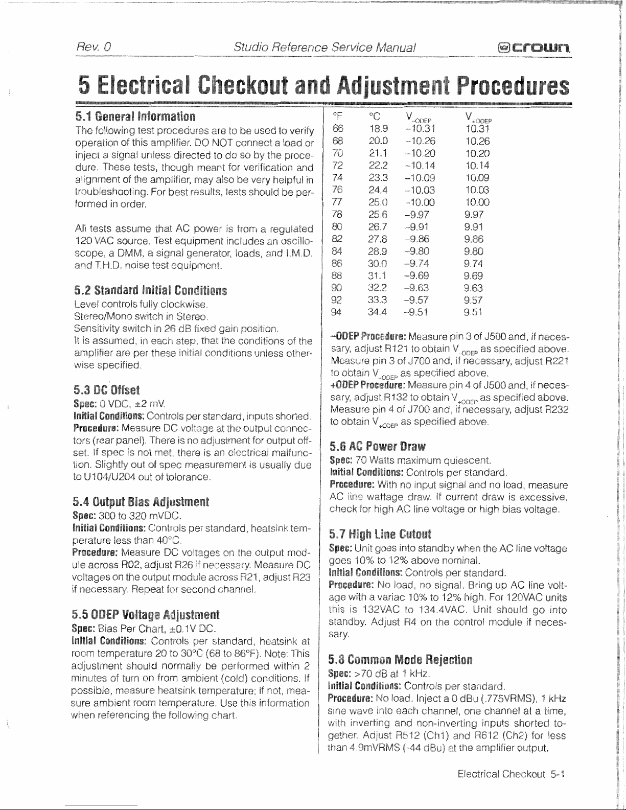
R@K
0
----...,
...-
-
,,, ,, ,
-...I.....YIIIIIIIIIIllllYllllllYl
Studio
Reference
Service
, , ,,
Manual
-.,-
mcrmwn*
Checkou
Procedures
t8,9
-10.31
1039
28.0
--10"26
10+26
21.7
.-.18.28
18.20
22.2
--16.14
1Qs?4
23.3
.-"i.09
1Q,$39
25.0
--toO~W
1O.W
25,6
--9.97
9.97
26.7
--8,9l
9.91
2723
-.9+86
9.86
28,9
-9.80
9.80
30.0
-9.94
9.44
31.1
-9.69
9-69
5,2
Standard
initial
Cowdltigns
32.2
-9.63
9.63
Level
controls
fully
clockwise.
StereoBMano
switch
in
Stereo.
Sensitivity
switch
in
26
dB
fixed
gain
pasition.
It
is
assumed,
in
each
step,
that
Ehe
conditions
of
the
amplifier
are
per
these
initial
conditions
unless
other-
wise
specified,
-ODEP
Proe8Bure:
Measure
pin
3
of
3500
and,
if
news-
sary,
adjust
R121
to
obtain
V
,,,,
as
specified
above.
Measure
pin
3
of
J700
and,
if
necagsarx
adjust
R22t
to
obtain
V
,,,,
as
s~ecifred
above,
5,3
QC
Offset
+OOEP
~rocgiite:
~easure
pin
4
of
3500
and,
if
neces-
sary,
adjust
R132
to
obtain
V+,,,,
as
specified
above.
Spgc;
8 WBC,
k2
rnV
Measure
pin
4 of
J700
and,
if
necessary,
adjust
R232
lnltial
Ce~dttOax~gr
Controls
per
standard,
mputs
shorted
oblasn
v+OL)EP
as
Preeadurs:
Msasure
DC
voltage
at
the
sutput
canncc-
tors
(rear
panel).
There
is
ns
adjustment
for
output
off-
set.
If
spec
is
not
met,
there
is
an
afectricai
rnaifunc-
tian,
Sligh8fy
out
of
spec
measurEment
is
usually
due
to
U"iQiU204
0165:
of
tolerance,
5.4
Output
Bias
Adjustment
Spec:
300
ta
320
rnVDC,
ilnitiall
Gandstiaa$::
Contrais
per
standard,
healsink
tern-
peratare
less
than
40°C
P~oeedurs:
Measwe
DC
voltages
or?
the
output
mod-
ule
across R02,
adjust
R26
if
B-eecessary,
Measure
DC
voltages
on
the
output
module
across
R21,
adjerst
R23
if
necessary.
Repeat
for
second
channel.
5,6
BC
Power
Draw
Spbc::
70
Wazrs
nmaximkam
quiescent.
initial
Csnditions:
Controls
per
standard.
Procedure:
With
no
input
si~nal
and
BBQ
16ad,
measure
AC
line
wattage
draw.
if
current
draw
is
excessive,
check.
far
high
AC
Iim
voltage
or
high
bias
vsitaga.
5.7
High
Line
Gutout
Spec:
Unit
goes
into
standby
when
the
AC
line
voftage
goes
^f
8%
to
to
12%
aabw
onominal,
lnltial
Gondltionsl:
Controls
par
standard.
Proeedgre:
No
load,
no
signal,
Bring
up
AC
line
volt-
age
with a variac
10%
to
12%
high.
Far
120VAC
units
5.5
ODEP
Voltage
Adjustment
this
is
132VAC
is
334.4VAC.
Unit
should
go
into
Spat:
Bias
Per
Chart,
~6,4V
DC.
standby.
Adjust
R4
sn
the
control
module
if
neees-
sary.
InltiaiP
@oiaridition%:
ContnaSs
per
standard,
heatsink
at
room
temperature
20
to
30°C
(68
to
86°F)"
Note:
This
adjustrnerr"rh8ufd
nsrmaliy
be
performed
wilhin
2
r~rintsts%
07
turn
an
from
ambient
(esfd)
cornditions,
If
possible,
measure
healsink
temperature;
if
not,
msa-
sure
ambient
room
temperature.
Use
this
infarmation
when referencing
the
$.a/lawing
chart,
5.8
Common
Mode
Reje~tion
Spac:
>70
dB
at
1
kHz,
initial
Cendilions:
Controls
per
standard,
Prosgdure:
No
load,
Inject
a
0
dBil(.775VRMS),
1
kHz
sine
wav@
into
each
channel,
one
channel
at
a
time,
wieh
inverting
and
non-inverting
inputs
shorted
to-
getkaer.
Adjust
R512
(Chl)
and
RE12
(Ch2)
for
less
than
4,9mVRMS
(-44
dBu)
at
the
amplifier
output.
Elcctrfcal
Checkout
5-1
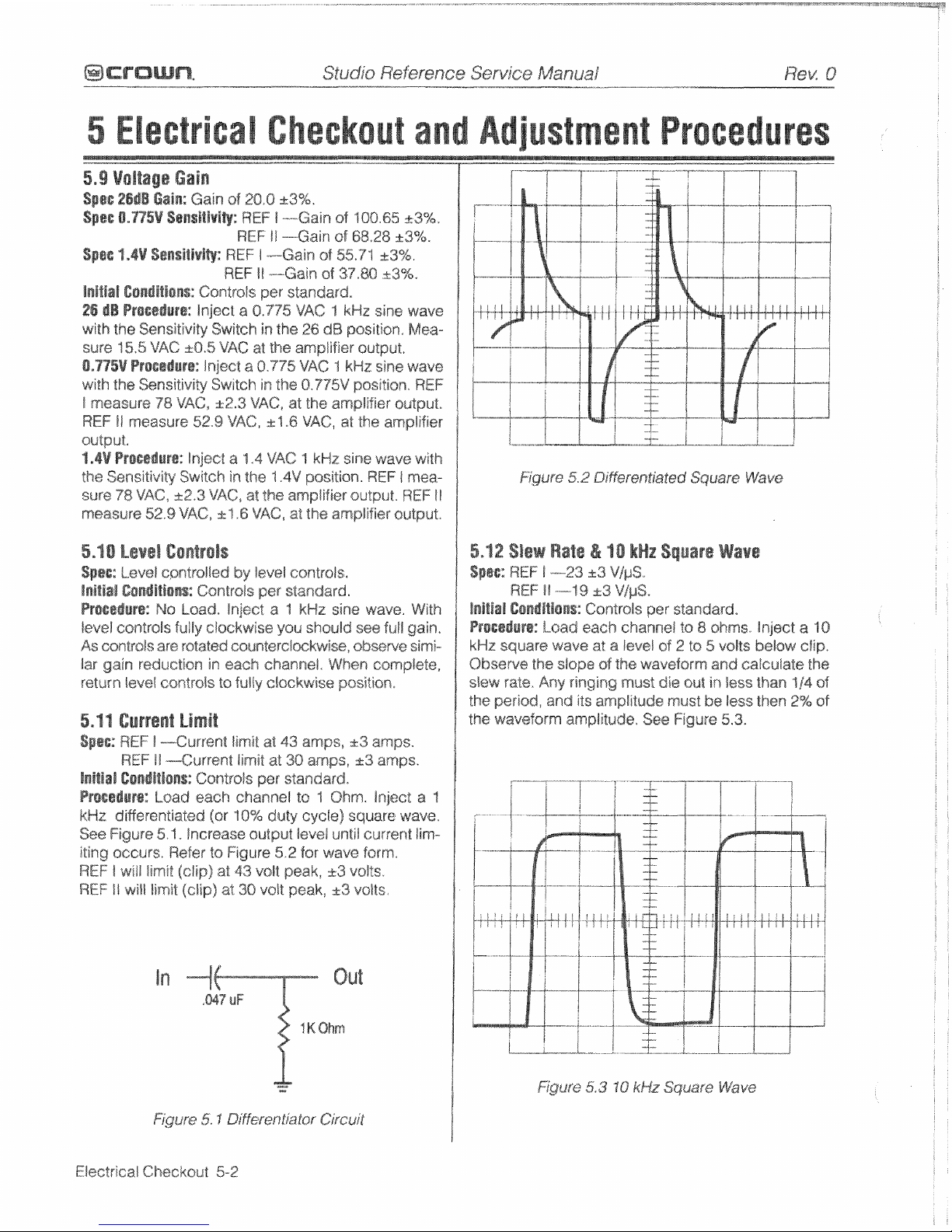
Gheckou
Procedures
5.9
Voltage
Gain
Spee
2666
Gg%n;
Gain
of
20,8
k3%.
Spac
0.775V
5e~%itlvi~:
REF
I
."---Gain
at
'508.65
&3%,
REF
!i
-~~~~~~~~~Eain
af
68,28
~3%.
Spec
1.4V
S~nsltivlQ:
REF
I
---Gain
of
5521
&3%.
REF
t
l
----Gain
st
37
.SO
a3%,
Inibtia%l
Eondlti@n%:
Controls
per standard.
26
dB
Procsduf@:
Inject
a
0,775
VAC
1
kHz
sine
wave
with
the Sensitivity
Switch
in
ths
26
dB
position,
Mea-
sure
15.5
VAC
f0.S
VAC
at
the
amplifier
skstpu2.
0,775V
Prosedut~::
Inject
a
0.775
VAC 1 kHz
sins
wave
with
the
Sensitivity
Switch
in
the
8.975V
position*
REF
i
measure
78
VAC,
f2.3
VAC,
at
Zh@
amplifies output.
REF
II
measure
52.9
VAC,
;s;.
"1.6
VACt
at
the
amplifier
output.
1
.@V
Bros@dure:
lnject
a
1,4
VAC
1
kHz
sine
wave
with
the
S~n~itisgify
Switch
in
the
1.4V
position.
REF
1
mea-
Figufe
5.2
DiF@r@nZia$ed
Square
Wave
sum
778
VAC,
&2,3
VAC,
st
the
amplifier
output.
REF
I!
measure
52.9
VACF A 1.6
VAC,
at
the amplifier
output*
5,10
Level
C~ntrsls
S@@s:
kevef
cantroiled
by
level
controls,
Inltlairl
Conditiows:
Controls
per
standard.
Bre@adur@:
No
Laad,
lnject
a
%
kHz
sine
wave.
With
level
controls
fully
clockwise
you
should
see
futf
gain,
As
controts
are
rotated
eountercixkwise,
sbsewe
sirni-
Iiar
gain
reduetisn
in
each
channel,
&$hen
complete,
return
!eve8
contrsls
$0
fully
clockwise
pssitian,
5,lf
Current
Limit
Spec:
REF
1
---Current
fimit
at
43
amps,
323
amps.
REF
II
-Current
limit
at
30
amps,
k3
amps,
lnrtlal
Csndftians:
ConWols
per
standard.
Procad&~s:
Load
each
channel
ta
7
Ohm.
Inject
at
"I
kHz
differentiated
&ear
38%
duty
cycte)
square
wave.
See
Figure
5%
f
.
Insrease
output
level
until
current
lim-
iting
occurs,
Refer
$0
Figure
52
for
wave
Form.
REF
f
will
limit
(clip)
at
43
vstt
peak,
2~3
voltss.
REF
II
will
limit
(clip)
at
38
v~iwpeak,
k3
volts,
In
-I
Out
5.12
Slsw
Rate
&
10
kHz
Square
Wave
Spac:
REF
1
-23
d3
V/pS.
REF
If
-1
9
~3
V&S.
lnltrai
eondltlo~s:
Cantrsls
per
standard,
F~ecedurg:
Laad
each
~hawwel
to
8
sk~rns.
inject
a
10
kHz
square
wave
at
a
level
of
2
ts
5
volts
below
clip.
Observe
the slope
af
the
waveform
and
catculate
the
sllew
rate,
Any
ringing
must
die
out
in
lass
than
"44
of
the
period,
and
its
amplitude
must
be
less
then
2%
aOf
%be
waveform
amplitude.
See
Figure
5.3.
Figure
5.3
IQ
kHz
Square
kVave
Electrical
Checkout
5-2
 Loading...