

Page 1

Power Base-1 & 460CSL Amplifier Service Manual
POWER AMPLIFIER
SERVICE MANUAL
POWER BASE-1® & 460CSL
©1995 by CROWN INTERNATIONAL, INC.
Mailing Address:
P.O. Box 1000
Elkhart, IN U.S.A. 46515-1000
Shipping Address:
57620 C.R. 105
Elkhart, IN U.S.A. 46517
™
CSL™ is a trademark and Power Base-1,® ODEP® and Crown® are registered trademarks of Crown International, Inc.
K-SVCPB1
1-95
1
Page 2

Power Base-1 & 460CSL Amplifier Service Manual
Table of Contents
Introduction .............................................................4
Scope......................................................................4
Warranty..................................................................4
Parts ........................................................................ 5
Specifications..........................................................6
Voltage Conversion ................................................. 7
Circuit Theory .......................................................... 8
Test Procedures.................................................... 13
Mechanical Parts Listing .......................................17
Module Information ...............................................20
Q42576-1 Output Module (Original) .....................21
Q42661-1 Output Module (#2) .............................. 22
Q42718-9 Output Module (#3) .............................. 23
Q42885-6 Output Module (TO-3P)........................24
Q42967-2 Output Module (THC)...........................25
Q43200-7 Output Module (THC #2)......................26
Q42552A0 Main Module (Original)........................27
Q42664-5 Main Module (Service Only) ................. 29
Q42682-7 Main Module (#2) .................................31
Q42776-7 Main Module (3rd Gain) ....................... 34
Q42953-2 Main Module (3rd Gain PB-1) .............. 37
Q43060-5 Main Module (THC) ..............................40
3
Page 3

Power Base-1 & 460CSL Amplifier Service Manual
Specifications
Unless noted otherwise, all specifications are based
on driving an 8 ohm load per channel, both channels
driven, the sensitivity switch in the 26dB position, the
AC supply is 120VAC at 60Hz. Crown specifications
are guaranteed through the warranty period (normally
3 years). Because our testing methods are more stringent than our published specifications, every Crown
amplifier will exceed its published specifications.
POWER
Power
8 Ohm Stereo—205W/Ch
4 Ohm Stereo—230W/Ch
8 Ohm Bridge Mono—430W
4 Ohm Parallel Mono—425W
Load Impedances: Rated for 16, 8, 4, and 2 (parallel
mono only) Ohm operation; safe with all types of loads,
even totally reactive loads.
AC Mains: 120VAC at 60 Hz with standard 3 wire
grounded 15A connector with single voltage transformer and fan for North American units; 100VAC,
120VAC, 220VAC, and 240VAC at 50 or 60 Hz when
equipped with universal transformer, applicable fan,
and other applicable hardware with country specific
power cord. Note that at 50 Hz fan speed is reduced.
PERFORMANCE
Frequency Response: ±0.1dB from 20 Hz to 20 kHz at 1
Watt.
Phase Response: ±10° from 10 Hz to 20 kHz at 1 Watt.
Signal to Noise Ratio: Better than 105 dB (A-weighted)
below max. average power from 20 Hz to 20 kHz.
Total Harmonic Distortion (THD): <0.05% from 20 Hz to
1 kHz, increasing linearly to 0.1% at 20 kHz at 170W.
I.M. Distortion: <0.05% from 10 milliwatts to 170W at 26
dB gain.
Slew Rate: >13V per microsecond.
Damping Factor: >1000 from 10 Hz to 400 Hz.
Input Impedance: Nominally 20K ohms balanced; 10K
ohms unbalanced.
Output Impedance: <10 milliohms in series with <2
microhenries.
Protection Systems: Output Device Emulation Protec-
tion (ODEP) limits drive in the event of dangerous
dynamic thermal conditions without interrupting power.
Current limiting for shorted load protection. DC/LF and
common mode output current Fault circuitry to mute
audio. Delay of 4 seconds from turn on mutes amplifier
to prevent dangerous turn-on transients. High voltage
fuse in main transformer primary and low voltage fuse
in fan primary. Slew rate limiting to prevent RF burn
out.
MECHANICAL
Input Connectors: Balanced 1/4 inch phone jacks.
Output Connectors: Color-coded 5-way binding posts
on 3/4 inch centers; spaced 3/4 inch apart.
Front Panel Controls: A rocker on/off power switch.
Back Panel Controls: A three-position switch which
selects Stereo, Bridge-Mono, or Parallel-Mono mode;
a two position input ground-lift switch, and level controls for each channel.
Internal Controls: A three-position switch selects 0.775V,
1.4V, or 26 dB voltage gain input sensitivity (all units
manufactured with D 7911-7 main module or later;
earlier models only allowed for 0.775V or 26 dB gain).
Indicators: Red Enable indicator shows on/off status of
low-voltage power supply.
Construction: Black splatter-coat steel chassis with
specially designed flow-through ventilation system.
Mounting: Standard EIA 310 front-panel rack mount
with supports for supplemental rear corner mounting.
Dimensions: 19 inches wide, 3.5 inches high, 16 inches
deep behind front mounting surface.
DC Offset: <10 millivolts.
6
Weight: 30 lbs.
Page 4

Power Base-1 & 460CSL Amplifier Service Manual
Voltage Conversion
PB/CSL Universal Fuse Board
BLU
BRN
P19
P20
P10
P9
P8
P7
P16
P15
P14
P13
P12
P11
P6
P5
P4
P3
P2
P1
P22
100V Connections:
P10 to P15
P11 to P14
P7 to P12
120V Connections:
P10 to P16
P11 to P14
P7 to P13
220V Connections:
P10 to P15
P9 to P14
P8 to P13
240V Connections:
P10 to P16
P9 to P14
P8 to P13
For list of applicable
transformer, fuse F100,
fanformer, and power
cord refer to voltageparts cross-reference.
F1F100
P18
S1 Power Switch
P17
Note: The only versions of this
product produced at the Crown
Factory with international voltage capabilities built in are CSL
versions built specifically for
sale outside the United States.
P21
Specific parts are required for the PB-1/460CSL in
order to be used at different international line voltages. Refer also to Mechanical Parts Lists.
100V AC Mains:
10A Fuse A10285-26
0.5A Low Voltage Supply Fuse A10285-7
Power Transformer (Universal) D 7598-2
Transmotor 120V 50 Hz H43055-5
120V AC Mains:
10A Fuse A10285-26
0.5A Low Voltage Supply Fuse A10285-7
Power Transformer (Universal) D 7598-2
Power Transformer (United States) D 6589-2
Transmotor 120V 50 Hz H43055-5
Transmotor 120V 60 Hz H43065-4
220V to 240V AC Mains:
5A Fuse A10285-21
0.5A Low Voltage Supply Fuse A10285-7
Power Transformer D 7598-2
Transmotor 120V 50 Hz H43055-5
7
Page 5

Power Base-1 & 460CSL Amplifier Service Manual
Theory
OVERVIEW
It should be noted from the outset that the PB-1 and
460CSL amplifiers are electrically and mechanically
identical products. The only differences, from a service perspective, are cosmetic. For the purposes of
servicing the products, it should also be known that
the CSL version has been on the market since 1992.
Since the PB amplifiers have been in production since
the mid-1980’s there are a number of electrical and
mechanical parts associated with the older PB models
only. It is also important to realize that over time Crown
has introduced numerous improvements to PB/CSL
amplifiers. Though often changes are minor, and are
made for a variety of reasons, a few changes have had
a significant impact on the operation of the circuitry.
This manual is up to date as of the time of writing. For
additional information regarding these amplifiers, refer to the applicable Technical Notes provided by
Crown for this product.
This section of the manual explains the general operation of a typical Crown power amplifier. Topics covered include Front End, Grounded Bridge, and ODEP.
Due to variations in design from vintage to vintage
(and similarities with other products Crown) the theory
of operation remains simplified.
FEATURES
Power Base/CSL amplifiers utilize numerous Crown
innovations including grounded bridge and ODEP
technologies. Cooling techniques make use of the
what is essentially air conditioner technology. Air flows
bottom to top, and front to side. Air flows a short
distance across a wide heatsink. This type of air flow
provides significantly better cooling than the “wind
tunnel” technology used by many other manufacturers. Output transistors are of the metal can type rather
than plastic case. This allows for a significantly higher
thermal margin for the given voltage and current
ratings. All devices used are tested and graded to
ensure maximum reliability. Another electronic technique used is negative feedback. Almost all power
amplifiers utilize negative feedback to control gain
and provide stability, but Crown uses multiple nested
feedback loops for maximum stability and greatly
improved damping. Most Crown amplifiers have damping in excess of 1000 in the bass frequency range. This
feedback, along with our compensation and ultra-low
distortion output topology, make Crown amplifiers
superior.
Features specific to the Power Base/CSL Series’ in-
clude a single core transformer (one primary with two
independent ungrounded secondaries), a full time full
speed fan which also serves as the low voltage
transformer, slew rate limiting, and audio muting for
delay or protective action. This amplifier can operate
in either a Bridged or Parallel Mono mode as well as
dual (stereo). A sensitivity switch allows selection of
input voltage required for rated output. Level controls
are rear mounted. The only indicator provided tells the
operator that the low voltage supply is energized. In
general, the packaging of this model is designed for
maximum watt/price/weight/size value. It is the most
basic grounded bridge amplifier now available from
Crown.
For additional details refer to the specification section,
or to the applicable Owner’s Manual.
FRONT END OPERATION
The front end is comprised of three stages: Balanced
Gain Stage (BGS), Variable Gain Stage (VGS), and
the Error Amp. Figure 1 shows a simplified diagram of
a typical front end with voltage amplification stages.
Balanced Gain Stage (BGS)
Input to the amplifier is balanced. The shield may be
isolated from chassis ground by an RC network to
interrupt ground loops (early models did not have the
Ground Lift feature) via the Ground Lift Switch. The
non-inverting (hot) side of the balanced input is fed to
the non-inverting input of the first op-amp stage. The
inverting (negative) side of the balanced input is fed
to the inverting input of the first op-amp stage. A
potentiometer is provided for common mode rejection
adjustment. Electrically, the BGS is at unity gain.
(From an audio perspective, however, this stage
actually provides +6dB gain if a fully balanced signal
is placed on its input.) The BGS is a non-inverting
stage. It’s output is delivered to the Variable Gain
Stage.
Variable Gain Stage (VGS)
Note: Older models only had two front end stages.
The functions of this stage were combined, primarily,
with those of the third.
From the output of the BGS, the signal goes to the VGS
where gain is determined by the position of the Sensitivity Switch, and level is determined by the level
control. VGS is an inverting stage with the input being
fed to its op-amp stage. Because gain after this stage
is fixed at 26dB (factor of 20), greater amplifier sensi-
8
Page 6

Power Base-1 & 460CSL Amplifier Service Manual
Theory
tivity is achieved by controlling the ratio of feedback to
input resistance. The Sensitivity Switch sets the input
impedance to this stage and varies the gain such that
the overall amplifier gain is 26 dB, or is adjusted
appropriately for 0.775V or 1.4V input to attain rated
output. Note that earlier models (before main modules
built with D 7911-7 board) did not support the 1.4V
sensitivity.
Error Amp
The inverted output from the VGS is fed to the noninverting input of the Error Amp op-amp stage through
an AC coupling capacitor and input resistor. Amplifier
output is fed back via the negative feedback (NFb)
loop resistor. The ratio of feedback resistor to input
resistor fixes gain from the Error Amp input to the
output of the amplifier at 26 dB. Diodes prevent
overdriving the Error Amp. Because the Error Amp
amplifies the difference between input and output
signals, any difference in the two waveforms will
produce a near open loop gain condition which in turn
results in high peak output voltage. The output of the
Error Amp, called the Error Signal (ES) drives the
Voltage Translators.
VOLTAGE AMPLIFICATION
The Voltage Translator stage separates the output of
the Error Amp into balanced positive and negative
drive voltages for the Last Voltage Amplifiers (LVAs),
translating the signal from ground referenced ±15V to
±Vcc reference. LVAs provide the main voltage amplification and drive the High Side output stages. Gain
from Voltage Translator input to amplifier output is a
factor of 25.2.
Voltage Translators
A voltage divider network splits the Error Signal (ES)
into positive and negative drive signals for the balanced voltage translator stage. These offset reference
voltages drive the input to the Voltage Translator
transistors. A nested NFb loop from the output of the
amplifier mixes with the inverted signal riding on the
offset references. This negative feedback fixes gain at
the offset reference points (and the output of the Error
Amp) at a factor of -25.2 with respect to the amplifier
output. The Voltage Translators are arranged in a
common base configuration for non-inverting voltage
gain with equal gain. They shift the audio from the
±15V reference to VCC reference. Their outputs drive
their respective LVA.
Also tied into the Voltage Translator inputs are ODEP
limiting transistors and control/protection transistors.
The ODEP transistors steal drive as dictated by the
ODEP circuitry (discussed later). The control/protection transistors act as switches to totally shunt audio to
ground during the turn-on delay, or during a DC/LF or
Fault protective action.
Last Voltage Amplifiers (LVAs)
The Voltage Translator stage channels the signal to
the Last Voltage Amplifiers (LVA's) in a balanced
configuration. The +LVA and -LVA, with their push-pull
effect through the Bias Servo, drive the fully complementary output stage. The LVAs are configured as
common emitter amplifiers. This configuration provides sufficient voltage gain and inverts the audio. The
polarity inversion is necessary to avoid an overall
polarity inversion from input jack to output jack, and it
Audio
Inputs
BGS VGS Error
Amp
+
-
+
-
+
-
Figure 1. Typical Amplifier Front End and Voltage Amplification Stages.
+15V
Voltage Divider
+
-15V
-
ODEP
Q100
Q103
Mute
Q121
Q122
NFb Loop
Voltage
Translators
Q101
Q102
+VCC
Q105
NPN Outputs (+HS)
PNP Outputs (-HS)
Q110
-VCC
LVA's
9
Page 7

Power Base-1 & 460CSL Amplifier Service Manual
Theory
allows the NFb loop to control Error Amp gain by
feeding back to its non-inverting input (with its polarity
opposite to the output of the VGS). With the added
voltage swing provided by the LVAs, the signal then
gains current amplification through the Darlington
emitter-follower output stage.
GROUNDED BRIDGE TOPOLOGY
Figure 2 is a simplified example of the grounded
bridge output topology. It consists of four quadrants
of three deep Darlington (composite) emitter-follower
stages per channel: one NPN and one PNP on the
High Side of the bridge (driving the load), and one
NPN and one PNP on the Low Side of the bridge
(controlling the ground reference for the rails). The
output stages are biased to operate class AB+B for
ultra low distortion in the signal zero-crossing region
and high efficiency.
High Side (HS)
The High Side (HS) of the bridge operates much like
a conventional bipolar push-pull output configuration.
As the input drive voltage becomes more positive, the
HS NPN conducts and delivers positive voltage to the
load. Eventually the NPN devices reach full conduction and +Vcc is across the load. At this time the HS
PNP is biased off. When the drive signal is negative
going, the HS PNP conducts to deliver -Vcc to the load
and the HS NPN stage is off.
The output of the +LVA drives the base of predriver
device. Together, the predriver and driver form the
first two parts of the three-deep Darlington and are
biased class AB. They provide output drive through
the bias resistor, bypassing the output devices, at
levels below about 100mW. An RLC network between
the predriver and driver provide phase shift compensation and limit driver base current to safe levels.
Output devices are biased class B, just below cutoff.
At about 100mW output they switch on to conduct high
current to the load. Together with predriver and driver,
the output device provide an overall class AB+B
output.
The negative half of the HS is almost identical to the
positive half, except that the devices are PNP. One
difference is that the PNP bias resistor is slighter
greater in value so that PNP output devices run closer
to the cutoff level under static (no signal) conditions.
This is because PNP devices require greater drive
current.
HS bias is regulated by Q18, the Bias Servo. Q18 is a
Vbe multiplier which maintains approximately 3.3V
Vce under static conditions. The positive and negative
halves of the HS output are in parallel with this 3.3V.
With a full base-emitter on voltage drop across
predrivers and drivers, the balance of voltage results
in approximately .35V drop across the bias resistors in
10
+
+Vcc (Positive Rail)
Input
signal
HIGH SIDE LOW SIDE
Load
(speaker)
-Vcc (Negative Rail)
Inverting Op-amp
-
Figure 2. Crown Patented Grounded Bridge Topology
Page 8

Power Base-1 & 460CSL Amplifier Service Manual
Theory
the positive half, and about .5V across the bias resistor
in the negative half. Q18 conduction (and thus bias) is
adjustable.
A diode string prevents excessive charge build up
within the high conduction output devices when off.
Flyback diodes shunt back-EMF pulses from reactive
loads to the power supply to protect output devices
from dangerous reverse voltage levels. An output
terminating circuit blocks RF on output lines from
entering the amplifier through its output connectors.
Low Side (LS)
The Low Side (LS) operates quite differently. The
power supply bridge rectifier is not ground referenced, nor is the secondary of the main transformer.
In other words, the high voltage power supply floats
with respect to ground, but ±Vcc remain constant with
respect to each other. This allows the power supply to
deliver +Vcc and -Vcc from the same bridge rectifier
and filter as a total difference in potential, regardless
of their voltages with respect to ground. The LS uses
inverted feedback from the HS output to control the
ground reference for the rails (±Vcc). Both LS quadrants are arranged in a three-deep Darlington and are
biased AB+B in the same manner as the HS.
When the amplifier output swings positive, the audio is
fed to an op-amp stage where it is inverted. This
inverted signal is delivered directly to the bases of the
positive (NPN) and negative (PNP) LS predrivers. The
negative drive forces the LS PNP devices on (NPN
off). As the PNP devices conduct, Vce of the PNP
Darlington drops. With LS device emitters tied to
ground, -Vcc is pulled toward ground reference.
Since the power supply is not ground referenced (and
the total voltage from +Vcc to -Vcc is constant) +Vcc
is forced higher above ground potential. This continues until, at the positive amplifier output peak, -Vcc =
0V and +Vcc equals the total power supply potential
with a positive polarity. If, for example, the power
supply produced a total of 70V from rail to rail (±35VDC
measured from ground with no signal), the amplifier
output would reach a positive peak of +70V.
Conversely, during a negative swing of the HS output
where HS PNP devices conduct, the op-amp would
output a positive voltage forcing LS NPN devices to
conduct. This would result in +Vcc swinging toward
ground potential and -Vcc further from ground potential. At the negative amplifier output peak, +Vcc = 0V
and -Vcc equals the total power supply potential with
a negative polarity. Using the same example as above,
a 70V supply would allow a negative output peak of 70V. In summary, a power supply which produces a
total of 70VDC rail to rail (or ±35VDC statically) is
capable of producing 140V peak-to-peak at the amplifier output when the grounded bridge topology is
used. The voltage used in this example are relatively
close to the voltages of the PB-1/460CSL.
The total effect is to deliver a peak to peak voltage to
the speaker load which is twice the voltage produced
by the power supply. Benefits include full utilization of
the power supply (it conducts current during both
halves of the output signal; conventional designs
require two power supplies per channel, one positive
and one negative), and never exposing any output
device to more than half of the peak to peak output
voltage (which does occur in conventional designs).
Low side bias is established by a diode string which
also shunts built up charges on the output devices.
Bias is adjustable via potentiometer. Flyback diodes
perform the same function as the HS flybacks. The
output of the LS is tied directly to chassis ground via
ground strap.
OUTPUT DEVICE EMULATION PROTECTION
(ODEP)
To further protect the output stages, a specially developed ODEP circuit is used. It produces a complex
analog output signal. This signal is proportional to the
always changing safe-operating-area margin of the
output transistors. The ODEP signal controls the Voltage Translator stage by removing drive that may
exceed the safe-operating-area of the output stage.
ODEP senses output current by measuring the voltage dropped across LS emitter resistors. LS NPN
current (negative amplifier output) and +Vcc are
sensed, then multiplied to obtain a signal proportional
to output power. Positive and negative ODEP voltages
are adjustable via two potentiometers. Across ±ODEP
are a PTC and a thermal sense (current source). The
PTC is essentially a cutoff switch that causes hard
ODEP limiting if heatsink temperature exceeds a safe
maximum, regardless of signal level. The thermal
sense causes the differential between +ODEP and –
ODEP to decrease as heatsink temperature increases.
An increase in positive output signal output into a load
will result in –ODEP voltage dropping; an increase in
negative output voltage and current will cause +ODEP
voltage to drop. A complex RC network between the
11
Page 9

Power Base-1 & 460CSL Amplifier Service Manual
Theory
±ODEP circuitry is used to simulate the thermal barriers between the interior of the output device die
(immeasurable by normal means) and the time delay
from heat generation at the die until heat dissipates to
the thermal sensor. The combined effects of thermal
history and instantaneous dynamic power level result
in an accurate simulation of the actual thermal condition of the output transistors.
BALANCED
INPUTS
+VOLTAGE
TRANSLATOR
VGSBGS
-1
ERROR
AMP
OUTPUT
DEVICE
EMULATION
PROTECTION
-VOLTAGE
TRANSLATOR
+LVA
-1
HIGH SIDE
BIAS
SERVO
-LVA
-1
MAIN NEGATIVE FEEDBACK (NFb) LOOP
LOW SIDE
-1
INVERTING
BRIDGE
BALANCE
BIAS
DIODE
STRING
POSITIVE
HIGH SIDE
OUTPUT
NPN STAGE
NEGATIVE
HIGH SIDE
OUTPUT
PNP STAGE
POSITIVE
LOW SIDE
OUTPUT
NPN STAGE
NEGATIVE
LOW SIDE
OUTPUT
PNP STAGE
12
Figure 3. Typical Crown Amplifier Basic Block Diagram (One Channel Shown)
Page 10

Power Base-1 & 460CSL Amplifier Service Manual
Checkout Procedures
GENERAL INFORMATION
The following test procedures are to be used to verify
operation of this amplifier. DO NOT connect a load or
inject a signal unless directed to do so by the procedure. These tests, though meant for verification and
alignment of the amplifier, may also be very helpful in
troubleshooting. For best results, tests should be
performed in order.
All tests assume that AC power is from a regulated 120
VAC source. Test equipment includes an oscilloscope, a DMM, a signal generator, loads, and I.M.D.
and T.H.D. noise test equipment.
STANDARD INITIAL CONDITIONS
Level controls fully clockwise.
Stereo/Mono switch in Stereo.
Sensitivity switch in 26 dB fixed gain position.
It is assumed, in each step, that conditions of the
amplifier are per these initial conditions unless otherwise specified.
TEST 1: DC OFFSET
Spec: 0 VDC, ±10 mV.
Initial Conditions: Controls per standard, inputs shorted.
Procedure: Measure DC voltage at the output connec-
tors (rear panel). There is no adjustment for output
offset. If spec is not met, there is an electrical malfunction. Slightly out of spec measurement is usually due
to U104/U204 out of tolorance.
The following is a list of ODEP Bias Voltages VS.
Temperature.
°F °C V
–ODEP
V
+ODEP
66 18.9 –10.31 11.41
68 20.0 –10.26 11.36
70 21.1 –10.20 11.30
72 22.2 –10.14 11.24
74 23.3 –10.09 11.19
76 24.4 –10.03 11.13
77 25.0 –10.00 11.10
78 25.6 –9.97 11.07
80 26.7 –9.91 11.01
82 27.8 –9.86 10.96
84 28.9 –9.80 10.90
86 30.0 –9.74 10.84
88 31.1 –9.69 10.79
90 32.2 –9.63 10.73
92 33.3 –9.57 10.67
94 34.4 –9.51 10.61
–ODEP Procedure: Measure pin 6 of U100 and, if
necessary, adjust R121 to obtain V
as specified
–ODEP
above. Measure pin 6 of U200 and, if necessary,
adjust R221 to obtain V
as specified above.
–ODEP
+ODEP Procedure: Measure pin 6 of U103 and, if
necessary, adjust R132 to obtain V
as specified
+ODEP
above. Measure pin 6 of U203 and, if necessary,
adjust R232 to obtain V
as specified above.
+ODEP
TEST 2: OUTPUT BIAS ADJUSTMENT
Spec: 300 to 310 mVDC.
Initial Conditions: Controls per standard, heatsink tem-
perature less than 40°C.
Procedure: Measure DC voltages on the output module
across R31, adjust R26 if necessary. Measure DC
voltages on the output module across R32, adjust R23
if necessary. Repeat for second channel.
TEST 3: ODEP VOLTAGE ADJUSTMENT
Spec: Cold Bias Per Charts Below ±0.1V DC.
Initial Conditions: Controls per standard, heatsink at
room temperature 20 to 30°C (68 to 86°F). Note: This
adjustment should normally be performed within 2
minutes of turn on from ambient (cold) conditions. If
possible measure heatsink temperature, if not measure ambient room temperature. Use this information
when referencing the chart below.
13
Page 11

Power Base-1 & 460CSL Amplifier Service Manual
Checkout Procedures
TEST 4: AC POWER DRAW
Spec: 90 Watts maximum quiescent.
Initial Conditions: Controls per standard.
Procedure: With no input signal and no load, measure
AC line wattage draw. If current draw is excessive,
check for high AC line voltage or high bias voltage.
TEST 5: COMMON MODE REJECTION
Spec at 100 Hz: –70 dB.
Spec at 20 kHz: –50 dB.
Initial Conditions: Controls per standard.
Procedure: No load. Inject a 0 dBu 100 Hz sine wave
into each channel, one channel at a time, with inverting
and non-inverting inputs shorted together. At the
output measure less than –44 dBu. Inject a 0 dBu 20
kHz sine wave into each channel, one channel at a
time, with inverting and non-inverting inputs shorted
together. At the output measure less than –24 dBu.
Adjust R921 or R1021, if necessary, to obtain the
required measurements. (In older units the adjustments are done using N100/N200.)
TEST 6: VOLTAGE GAIN
Spec: ±3% when the Sensitivity Switch is set for 26dB
gain, ±6% when the Sensitivity Switch is set for 0.775V
or 1.4V sensitivity.
Initial Conditions: Controls per standard.
Procedure: No load connected. Inject a 0.775 VAC 1
kHz sine wave with the Sensitivity Switch in the 26 dB
position. Measure 15.5 VAC ±0.07 VAC at the amplifier output. Inject a 0.775 VAC 1 kHz sine wave with the
Sensitivity Switch in the 0.775V position. Measure 39.9
VAC ±1.2 VAC at the amplifier output. Inject a 1.4 VAC
1 kHz sine wave with the Sensitivity Switch in the 1.4V
position. Measure 39.9 VAC ±1.2 VAC at the amplifier
output. Return the Sensitivity Switch to the 26 dB
position.
TEST 7: PHASE RESPONSE
Spec: ±10° at 1 Watt.
Initial Conditions: Controls per standard, 8 ohm load on
each channel.
Procedure: Inject a 1 kHz sine wave and adjust for 1
Watt output (2.8 VAC). Check input and output signals
against each other, input and output signals must be
within 10° of each other.
Procedure: No Load. Inject a 1 kHz sine wave. With
level controls fully clockwise you should see full gain.
As controls are rotated counterclockwise, observe
similar gain reduction in each channel. When complete, return level controls to fully clockwise position.
TEST 9: CURRENT LIMIT
Spec: Current Limit at 13 ±2 Amps
Initial Conditions: Controls per standard.
Procedure: Load each channel to 1 Ohm. Inject a 1 kHz
differentiated (or 10% duty cycle) square wave and
increase output level until current limit occurs. Current
limit should occur at 11 ±1 Amps. Observe clean (no
oscillations) current clipping.
TEST 10: SLEW RATE & 10 KHZ SQUARE WAVE
Spec: >13V/µS.
Initial Conditions: Controls per standard.
Procedure: Load each channel to 8 ohms. Inject a 10
kHz square wave to obtain 40 volts peak-to-peak at
each output. Observe the slope of the square wave. It
should typically measure 17 to 25 V/µS. Also, the
square wave must not include overshoot, ringing, or
any type of oscillation.
TEST 11: CROSSTALK
Spec: <33 mVAC at 20 kHz.
Initial Conditions: Controls per standard. Short input of
channel not driven.
Procedure: 8 ohm load on each channel. Inject a 20 kHz
sine wave into the Channel 1 input and increase output
level to 37.4 VAC. Measure less than 33 mVAC at the
output of Channel 2. Inject a 20 kHz sine wave into the
Channel 2 input and increase output level to 37.4 VAC.
Measure less than 33 mVAC at the output of Channel
1.
TEST 12: OUTPUT POWER
Spec at 8 Ohm Stereo: 205W at 0.1% THD.
Spec at 4 Ohm Stereo: 230W at 0.1% THD.
Initial Conditions: Controls per standard.
Procedure: Load each channel to 8 ohms. Inject a 1 kHz
sine wave and measure at least 40.5 VAC at the output
of each channel. Load each channel to 4 ohms. Inject
a 1 kHz sine wave and measure at least 30.3 VAC. All
power measurements must be at less than 0.1% THD.
TEST 8: LEVEL CONTROLS
Spec: Level controlled by level controls.
Initial Conditions: Controls per standard.
14
TEST 13: REACTIVE LOADS
Spec: No oscillations. Safe with all types of loads.
Initial Conditions: Controls per standard.
Page 12

Power Base-1 & 460CSL Amplifier Service Manual
Checkout Procedures
Procedure Capacitive: Load each channel to 8 ohms in
parallel with 2 µF. Inject a 20 kHz sine wave with 30
VAC output for 10 seconds.
Procedure Inductive: Load each channel to 8 ohms in
parallel with 159 µHenries. Inject a 1 kHz sine wave
with 15 VAC output for 10 seconds.
Procedure Torture: Load each channel with the primary
(red and black leads) of a DC-300A transformer (D
5781-6). Inject a 10 Hz sine wave at sufficient output
level to cause 3 to 5 flyback pulses, for 10 seconds.
Procedure Short: Inject a 60 Hz sine wave at 5 VAC.
After establishing signal, short the output for 10 seconds.
TEST 14: ODEP LIMITING
Spec: No oscillation on ODEP Limiting wave form;
either channel controls limiting in Parallel Mono Mode.
Initial Conditions: Controls per standard; rag or other
obstruction blocking fan so that it does not turn.
Procedure: Load the amplifier to 2 ohms on each
channel. Inject a 60 Hz sine wave and adjust for 15
Vrms at the output. After a few minutes observe a wave
form similar to Figure 4. Remove the input signal from
both channels and allow the amplifier to cool for a few
minutes. Switch the amplifier to Parallel Mono and
remove the load from Channel 1. Inject the signal into
Channel 1 and observe that ODEP limiting occurs at
the output of both channels. Remove the load from
Channel 2, and install the load on Channel 1. Again,
observe that both channels limit. Return all amplifier
controls to standard initial conditions. Remove the fan
obstruction.
TEST 15: LF PROTECTION
Spec: Amplifier mutes for low frequency.
Initial Conditions: Controls per standard.
Procedure: No load. Inject a 0.5 Hz 6 volt peak-to-peak
square wave into each channel and verify that each
channel cycles into mute.
TEST 16: SIGNAL TO NOISE RATIO
Spec: 100 dB (105 dB A-weighted) below rated 8 ohm
power.
Initial Conditions: Controls per standard. Short inputs.
Procedure: Load each channel to 8 ohms. Measure
less than 400 µV at the output of each channel (or –100
dB from reference of +34.25 dBu).
TEST 17: TURN ON TRANSIENTS
Spec: No dangerous transients.
Initial Conditions: Controls per standard.
Procedure: From an off condition, turn on the amplifier
and monitor the output noise at the time of turn on.
Note: Turn on noise may increase significantly if the
amplifier is cycled off and on.
TEST 18: TURN OFF TRANSIENTS
Spec: No dangerous transients.
Initial Conditions: Controls per standard.
Procedure: From an on condition, turn off the amplifier
and monitor the output noise at the time of turn off.
Note: Turn off noise may increase significantly if the
amplifier is cycled off and on.
TEST 19: INTERMODULATION DISTORTION
Spec at 0 dB Output: 0.01%.
Spec at –35 dB Output: 0.05%.
Initial Conditions: Controls per standard.
Procedure: Load each channel to 8 ohms. Inject a
SMPTE standard IM signal (60 Hz and 7 kHz sine wave
mixed at 4:1 ratio) at 200 Watts (32.4 VAC). With an IM
analyzer measure less than 0.01% IMD. Repeat test at
–35 dB (reference 200 Watts or 32.4 VAC) and measure less than 0.05% IMD.
Figure 4. ODEP Limiting Wave Form
TEST 20: CLIPPING
Spec: No protective action during test.
Initial Conditions: Controls per standard.
Procedure: Load each channel to 8 ohms. Inject a 1 kHz
sine wave at each input and drive output 6 dB into clip
for 10 seconds. The amplifier should not activate any
protective circuits (ODEP, Fault, or LF Protection).
POST TESTING
After completion of testing, if all tests are satisfactory,
the amplifier controls should be returned to the positions required by customer. If conditions are unknown
or unspecified, factory settings are as follows:
15
Page 13

Power Base-1 & 460CSL Amplifier Service Manual
Mechanical (Non-Module) Parts
SUPPLIMENTAL ITEMS
CPN ITEM QTY
D 4137-2 Nylon Thumbscrew Washer 4
C 3342-0 Feet, Black Self-Stick 4
A10087-71012 10-32 .75 Machine (Rack Screw) 4
120VAC/60HZ NORTH AMERICA PRODUCT ONLY
CPN ITEM QTY
A10285-26 Fuse, 10A 3AB (120V Units) 1
A10285-7 Fuse, .5A AGC 1.25x.25 (LVPS) 1
D 6589-2 PB-1 Power Transformer 1
A10101-19 Washer, Fiber (XFMR Assby) 2
H42873-2 Fanformer Assembly 1
P10391-4 Fuse Board (U.S. Only) 1
P10426-6 Fuse Board (International Only) 1
FANFORMER MECHANICAL ASSEMBLY
CPN ITEM QTY
C 7062-0 Screw, 6-32-5/16 Flat Mach 2
C 9939-7 Fan Blade, 4 inch CCW 1
D 8439-8 Fan Bracket 1
FILTER CAPACITOR MOUNTING ASSEMBLY (ONE PER CHANNEL)
CPN ITEM QTY
A10095-4 Washer, #10 Ext. Lock 2
A10098-5 Belleville Spring Washer 2
C 7015-8 C126/C226 7800µF 90V 1
C 8752-5 D117/D217 35A 400V Bridge Rectifier 1
C 9870-4 Screw, 10-32-.38 Pan 2
D 6764-1 Washer, Shoulder 2
D 8438-0 Bracket, Capacitor Mounting 1
FUSE BOARD ASSEMBLY
CPN ITEM QTY
C 5060-6 Fuse Clip, PC Mount #926 4
P10391-4 Fuse Board 1
LED ASSEMBLY
CPN ITEM QTY
C 4342-9 Enable LED, Amber 1
P10068B4 LED Board 1
17
Page 14

Power Base-1 & 460CSL Amplifier Service Manual
Mechanical (Non-Module) Parts
OUTPUT ASSEMBLY (ONE PER CHANNEL)
CPN ITEM QTY
A10100-4 Washer, #6 Flat Zinc 2
A10315-1 Screw, 6-32-.56 Hex Washer Head 12
C 4751-1 NPN Output Device 2
C 5826-0 S100/S200 Thermal Sense LM334Z 1
C 6492-0 PNP Output Device 2
C 7326-9 Solder Lug, #6 Tin 2
C 8573-5 PNP Driver Device TO-3P 2
C 8574-3 NPN Driver Device TO-3P 2
C 8813-5 Q318/Q418 Bias Servo MPSA18/MPS8097 1
C 9491-9 Screw, 6-32-.312 Taptite Pan Ph 13
D 7665-9 Clip, TO-3P Mounting 2
D 7666-7 Bracket, TO-3P Heatsink 2
D 7796-2 Silpad Insulator 1
D 7797-0 Output Thru-Hole Pad Insulator 1
D 8264-0 PTC Thermal Sensor 1
F12019-0 Diode Heatsink Slug 1
F12469-7 Heatsink, Aluminum 2
Output Module (See Module List) 1
BACK PANEL ASSEMBLY
CPN ITEM QTY
A10214-7 Strain Relief (Power Cord) 1
C 2823-0 Dual Binding Post Assembly 1
D 7074-4 Power Cord (3-14 15A USA) 1
M21208J9 Back Panel 1
A10019-8 Nut, #8 32-2 Captive 2
CHASSIS FRONT ASSEMBLY
CPN ITEM QTY
A10031-1 Nut, 8-32 Captive 4
A10090-70806 Screw, 8-32-.375 Mach Ph Oval (Grille) 3
A10090-70808 Screw, 8-32-.5 Mach Ph Oval 4
A10101-5 Washer, Nylon (Grille) 3
A10110-70605 Screw, 6-32-.312 Taptite Ph (Cover) 20
A10173-1 Clip, Grille Filter 3
D 6944-9 Air Filter 1
D 8465J2 End Cap 2
D 8501-5 Cover , Top 1
D 8548-6 Cover, Bottom 1
F10962-3 Front Panel Overlay PB-1 1
F11978J7 Front Panel Overlay 460CSL 1
F12435J7 Grille 1
18
Page 15

Power Base-1 & 460CSL Amplifier Service Manual
Mechanical (Non-Module) Parts
MAIN CHASSIS ASSEMBLY
CPN ITEM QTY
A10086-11008 Screw, 10-32-.5 Mach Rd Ph 4
A10086-70806 Screw, 8-32-.37 Mach Rd Ph 2
A10089-11032 Screw, 10-32-2 Mach Pan Ph 4
A10094-3 Washer, #6 Black Star 3
A10094-6 Washer, #8 Black Star 4
A10094-8 Washer, #10 Tooth Lock 10
A10099-7 Washer, #10 Nylon Shoulder 4
A10100-16 Washer 4
A10102-8 Nut, 10-32 Hex Zinc 6
A10109-10822 Screw, 8-18-1.375 Pan Ph 2
A10110-70812 Screw, 8-32-.75 Taptite Pan Ph 2
A10192-1 Snap Bushing .5 4
C 1811-6 Tie Wrap 4
C 3163-0 Solder Lug #6 505 1
C 6487-0 Power Switch 22A Rocker 2 Pole 1
C 6912-7 Tension Retainer Board Support 2
C 6913-5 Spacer Nut, 1 inch 2
C 6914-3 Spacer Nut, .75 inch 2
C 9491-9 Screw, 6-32-.312 Taptite Pan 4
C 9953-8 Screw, 6-20-.312 Taptite Pan Black 6
D 7340-9 Label, F1 Fuse Replacement 1
D 7600-6 Ground Strap (DBP to Chassis) 1
D 7784-8 Label, Sensitivity Switch 1
D 8003-2 Label, F200 Fuse Replacement 1
D 8069-4 Insulator, Fuse Board 1
F10787J3 Back Panel Plate 1
F10963-1 Transformer Plate 1
M21059J6 Chassis 1
Main Module (See Module List) 1
19
Page 16

Power Base-1 & 460CSL Amplifier Service Manual
Module Information
MODULE HISTORY
Since its introduction in 1986, the PB-1 has gone
through a number of updates and revisions. Over the
course of its history some of these changes have
resulted in upgrading to newer modules. What follows
is a historical breakdown of PB-1 modules. It should
also be noted that the 460CSL was introduced in 1992
and therefor modules obsoleted before that time were
never used in the CSL version.
OUTPUT MODULES:
Q42576-1
Original output module. No longer available.
Q42661-1
Through hole output module. No longer available.
Q42718-9
Output module: 4 resistor small predriver. PB-1 Only.
Last output module for PB-1 for use with TO-220
package driver transistors.
Q42885-6
TO-3P Driver Output module. Not for use in THC units,
not retrofittable into TO-220 driver transistor units.
Q42967-2
THC Output module with TO-3P drivers. Not retrofittable
to any older units. Does not require special main
module for THC ODEP recompensation. Also improved bias stability.
Q43200-7
THC #2 Output Module. Replaces Q42967-2 only.
Electrically identical, but larger screw head plates
prevent shorting which could occur with the first THC
output module.
MAIN MODULES:
Q42552A0
This was the original main board. It offered 2 front end
gain stages and was also used in the PB-1, MT-600/
LX, MT-1200/LX. It did not include ground lift, but did
offer a choice of .775V or 26 dB voltage gain sensitivities. No longer available.
Q42664-5
Service replacement for Q42552A0 for PB-1. No longer
available.
Q42682-7
Main #2. Upgraded board from Q42552A0 for PB-1.
No longer available.
Q42776-7
Universally usable PC board, finished module used in
MT-600/1200, MA-600/1200, and PB-1. Added third
gain stage and ground lift switch. For use in the PB-1
install two level pots (C 7409-3) and remove R187 and
R287. Can replace all older modules. Use this module
to replace this or any previous module. This module
can also be used to replace the Q42953-2 module put
into production later. Note that if this module is being
used to replace an older module, you may have to
slide the ground lift switch to the left (ground lift
position) and clip off the plastic switch protrusion in
order for the module to properly fit in the unit.
Q42953-2
PB-1 main module to replace Q42776-7. This or the
Q42776-7 module may be used with TO-3P driver
transistor output modules, and with or without Through
Hole Chassis (THC) in this amplifier.
Q43060-5
THC main module built on D 7993-5 circuit board. On
this module the boost circuit has been deleted, the
third position (1.4V) is added to the Sensitivity Switch,
and additional fault circuitry has been added to the
module. Although it is possible to modify any older unit
to accept this module, it is recommended that the
Q42776-7 be used to replace main modules in all older
units, and this module be used only as a replacement
for itself.
20
Page 17

Power Base-1 & 460CSL Amplifier Service Manual
Q42576-1 Output Module Parts List (P10137-1 Board)
Q42576-1 Output Module (4 Resistor Original) for PB-1:
CAPACITORS
C01 C 3978-1 .047µF
C02 C 6804-6 .1µF
C03 C 6804-6 .1µF
C04 C 3996-3 .0047µF
C05 C 6807-9 .001µF
C06 C 6806-1 .01µF
C07 C 6807-9 .001µF
C08 C 6810-3 180pF
C09 C 6809-5 220pF
C43 C 6806-1 .01uF
DIODES
D01 C 2851-1 1N4004
D02 C 2851-1 1N4004
D03 C 2851-1 1N4004
D04 C 2851-1 1N4004
D05 C 2851-1 1N4004
D06 C 2851-1 1N4004
D07 C 2851-1 1N4004
D08 C 2851-1 1N4004
D09 C 2851-1 1N4004
D10 C 2851-1 1N4004
D11 C 2851-1 1N4004
D12 C 2851-1 1N4004
INDUCTORS
L00 C 6592-6 Output Coil
L01 C 3510-2 470µH
L02 C 3510-2 470µH
TRANSISTORS
Q17 C 3810-6 NPN MPSA43
Q19 C 3578-9 PNP MPSA93
RESISTORS
R00 A10266-7501 75
R01 A10266-4711 470
R02 C 7778-1 5.6
R03 C 6486-2 .2 5W
R08 C 6486-2 .2 5W
R09 C 7779-9 22
R10 A10266-4711 470
R11 C 1001-4 2.7 1W
R12 C 1001-4 2.7 1W
R13 A10266-7501 75
R14 C 1001-4 2.7 1W
R15 C 6486-2 .2 5W
R20 C 6486-2 .2 5W
R21 C 7778-1 5.6
R22 C 7779-9 22
R23 C 6844-2 250 Pot LS Bias
R24 A10266-1331 13K
R25 A10266-2221 2.2K
R26 C 6844-2 250 Pot HS Bias
R27 A10266-3911 390
R28 A10266-1331 13K
R30* A10265-10201* 102*
MISC.
Board P10137-1
Jumpers C 5868-2 0 Ohm Jumper (8)
Clips D 6414-3 Q17/19 Hold Down
J500 J600 C 7057-0 10 Pos. Connector
Note: R30 is 102 Ohms in most units, though in some
cases a different value may be used to match the
installed S100/S200 LM334 (C5826-0) device grade.
This is the standard value and is used with the most
common LM334 grade, green. If the LM334 is marked
with a blue dot, R30 should be a 107 Ohm resistor
(A10265-10701); if it is marked with a yellow dot then
R30 should be a 100 Ohm resistor (A10265-10001).
21
Page 18

Power Base-1 & 460CSL Amplifier Service Manual
Q42661-1 Output Module Parts List (P10137-1 Board)
Q42661-1 Output Module (4 Resistor #2) for PB-1:
CAPACITORS
C01 C 3978-1 .047µF
C02 C 6804-6 .1µF
C03 C 6804-6 .1µF
C04 C 3996-3 .0047µF
C05 C 6807-9 .001µF
C06 C 6806-1 .01µF
C07 C 6807-9 .001µF
C08 C 6810-3 180pF
C09 C 6809-5 220pF
DIODES
D01 C 2851-1 1N4004
D02 C 2851-1 1N4004
D03 C 2851-1 1N4004
D04 C 2851-1 1N4004
D05 C 2851-1 1N4004
D06 C 2851-1 1N4004
D07 C 2851-1 1N4004
D08 C 2851-1 1N4004
D09 C 2851-1 1N4004
D10 C 2851-1 1N4004
D11 C 2851-1 1N4004
D12 C 2851-1 1N4004
INDUCTORS
L00 C 6592-6 Output Coil
L01 C 3510-2 470µH
L02 C 3510-2 470µH
TRANSISTORS
Q17 C 3810-6 NPN MPSA43
Q19 C 3578-9 PNP MPSA93
RESISTORS
R00 A10266-7501 75
R01 A10266-4711 470
R02 C 7778-1 5.6
R07 D 6600-7 .19 5W
R09 C 7779-9 22
R10 A10266-4711 470
R11 C 1001-4 2.7 1W
R12 C 1001-4 2.7 1W
R13 A10266-7501 75
R14 C 1001-4 2.7 1W
R15 D 6600-7 .19 5W
R16 D 6600-7 .19 5W
R19 D 6600-7 .19 5W
R21 C 7778-1 5.6
R22 C 7779-9 22
R23 C 6844-2 250 Pot LS Bias
R24 A10266-1331 13K
R25 A10266-2221 2.2K
R26 C 6844-2 250 Pot HS Bias
R27 A10266-3911 390
R28 A10266-1331 13K
R30* A10265-10201* 102*
MISC.
Board P10137-1
Jumpers C 5868-2 0 Ohm Jumper (4)
Clips D 6414-3 Q17/19 Hold Down
J500 J600 C 7057-0 10 Pin Header
Note: R30 is 102 Ohms in most units, though in some
cases a different value may be used to match the
installed S100/S200 LM334 (C5826-0) device grade.
This is the standard value and is used with the most
common LM334 grade, green. If the LM334 is marked
with a blue dot, R30 should be a 107 Ohm resistor
(A10265-10701); if it is marked with a yellow dot then
R30 should be a 100 Ohm resistor (A10265-10001).
22
Page 19

Power Base-1 & 460CSL Amplifier Service Manual
Q42718-9 Output Module Parts List (P10233-8 Board)
Q42718-9 Output Module (4 Resistor #3) for PB-1:
CAPACITORS
C01 C 3978-1 .047µF
C02 C 3218-2 .22µF
C03 C 3218-2 .22µF
C04 C 8534-7 .0047µF
C05 C 6807-9 .001µF
C06 C 6806-1 .01µF
C07 C 6807-9 .001µF
C08 C 6810-3 180pF
C09 C 6809-5 220pF
DIODES
D01 C 2851-1 1N4004
D02 C 2851-1 1N4004
D03 C 2851-1 1N4004
D04 C 2851-1 1N4004
D05 C 2851-1 1N4004
D06 C 2851-1 1N4004
D07 C 2851-1 1N4004
D08 C 2851-1 1N4004
D09 C 2851-1 1N4004
D10 C 2851-1 1N4004
D11 C 2851-1 1N4004
D12 C 2851-1 1N4004
INDUCTORS
L00 C 6592-6 1.3µH Output Coil
L01 C 3510-2 470µH
L02 C 3510-2 470µH
TRANSISTORS
Q17 C 3810-6 NPN MPSA43/42
Q19 C 3578-9 PNP MPSA93
RESISTORS
R00 A10266-7501 75
R01 A10266-4711 470
R07 D 6600-7 .19 5W
R10 A10266-4711 470
R11 A10266-2R73 2.7 1W
R12 A10266-1204 12 2W
R13 A10266-7501 75
R14 A10266-1204 12 2W
R15 D 6600-7 .19 5W
R16 D 6600-7 .19 5W
R19 D 6600-7 .19 5W
R23 C 6844-2 250 Pot LS Bias
R24 A10266-1331 13K
R25 A10266-2221 2.2K
R26 C 6844-2 250 Pot HS Bias
R27 A10266-3911 390
R28 A10266-1331 13K
R30* A10265-10201* 102*
R31 C 7778-1 5.6 .5W Flame Proof
R32 C 7778-1 5.6 .5W Flame Proof
R33 C 7779-9 22 .5W Flame Proof
R34 C 7779-9 22 .5W Flame Proof
R35 A10266-1204 12 2W
R36 A10266-1204 12 2W
R37 A10266-1204 12 2W
R38 A10266-1204 12 2W
R39 A10266-1204 12 2W
R40 A10266-1204 12 2W
MISC.
Board P10233-8
Jumpers C 5868-2 0 Ohm .25W
Clips D 6414-3 Q17/Q19 Hold Down
J500 J600 C 7057-0 10 Pin Header
*Note: R30 is 102 Ohms in most units, though in some
cases a different value may be used to match the
installed S100/S200 LM334 (C5826-0) device grade.
This is the standard value and is used with the most
common LM334 grade, green. If the LM334 is marked
with a blue dot, R30 should be a 107 Ohm resistor
(A10265-10701); if it is marked with a yellow dot then
R30 should be a 100 Ohm resistor (A10265-10001).
23
Page 20

Power Base-1 & 460CSL Amplifier Service Manual
Q42885-6 Output Module Parts List (P10305-4 Board)
Q42885-6 Output Module (4 Resistor TO-3P Drivers) for
PB-1/460CSL:
CAPACITORS
C01 C 8511-5 .047µF
C02 C 7964-7 .22µF
C03 C 7964-7 .22µF
C04 C 8534-7 .0047µF
C05 C 6807-9 .001µF
C06 C 6806-1 .01µF
C07 C 6807-9 .001µF
C08 C 6810-3 180pF
C09 C 6809-5 220pF
C43 C 6806-1 .01uF
DIODES
D01 C 2851-1 1N4004
D02 C 2851-1 1N4004
D03 C 2851-1 1N4004
D04 C 2851-1 1N4004
D05 C 2851-1 1N4004
D06 C 2851-1 1N4004
D07 C 2851-1 1N4004
D08 C 2851-1 1N4004
D09 C 2851-1 1N4004
D10 C 2851-1 1N4004
D11 C 2851-1 1N4004
D12 C 2851-1 1N4004
INDUCTORS
L00 C 6592-6 Output Coil
L01 C 3510-2 470µH
L02 C 3510-2 470µH
TRANSISTORS
Q17 C 3810-6 NPN MPSA43
Q19 C 3578-9 PNP MPSA93
RESISTORS
R00 A10266-7501 75
R01 A10266-4711 470
R04 D 6600-7 .19 5W
R07 D 6600-7 .19 5W
R10 A10266-4711 470
R11 C 1001-4 2.7 1W
R12 C 3931-0 12 2W
R13 A10266-7501 75
R16 D 6600-7 .19 5W
R19 D 6600-7 .19 5W
R23 C 6844-2 250 Pot LS Bias
R24 A10266-1331 13K
R25 A10266-2221 2.2K
R26 C 6844-2 250 Pot HS Bias
R27 A10266-3911 390
R28 A10266-1331 13K
R29 C 6402-9 51 OHM
R30* A10265-10201* 102*
R31 C 7778-1 5.6 flame proof
R32 C 7778-1 5.6 flame proof
R33 C 7779-9 22 flame proof
R34 C 7779-9 22 flame proof
R35 C 3931-0 12 2W
R36 C 3931-0 12 2W
R37 C 3931-0 12 2W
R38 C 3931-0 12 2W
R39 C 3931-0 12 2W
R40 C 3931-0 12 2W
MISC.
Board P10305-4
Jumpers C 5868-2 0 Ohm Jumper (7)
Clips D 6414-3 Q17/19 Hold Down
J500 J600 C 7057-0 10 Pos. Connector
BEAD C 8341-7 Over emitter of Q19
Note: R30 is 102 Ohms in most units, though in some
cases a different value may be used to match the
installed S100/S200 LM334 (C5826-0) device grade.
This is the standard value and is used with the most
common LM334 grade, green. If the LM334 is marked
with a blue dot, R30 should be a 107 Ohm resistor
(A10265-10701); if it is marked with a yellow dot then
R30 should be a 100 Ohm resistor (A10265-10001).
24
Page 21

Power Base-1 & 460CSL Amplifier Service Manual
Q42967-2 Output Module Parts List (P10341-9 Board)
Q42967-2 Output Module for Through Hole Chassis (THC)
PB-1/460CSL units:
CAPACITORS
C01 C 8511-5 .047µF
C02 C 7964-7 .22µF
C03 C 7964-7 .22µF
C04 C 8534-7 .0047µF
C05 C 8534-7 .0047µF
C06 C 6806-1 .01µF
C07 C 6807-9 .001µF
C08 C 6810-3 180pF
C09 C 6809-5 220pF
C43 C 6806-1 .01µF
DIODES
D01 C 2851-1 1N4004
D02 C 2851-1 1N4004
D03 C 2851-1 1N4004
D04 C 2851-1 1N4004
D05 C 2851-1 1N4004
D06 C 2851-1 1N4004
D07 C 2851-1 1N4004
D08 C 2851-1 1N4004
D09 C 2851-1 1N4004
D10 C 2851-1 1N4004
D11 C 2851-1 1N4004
D12 C 2851-1 1N4004
INDUCTORS
L00 C 6592-6 Output Coil
L01 C 3510-2 470µH
L02 C 3510-2 470µH
TRANSISTORS
Q17 C 3810-6 NPN MPSA43
Q19 C 3578-9 PNP MPSA93
RESISTORS
R00 A10266-7501 75
R01 A10266-4711 470
R04 D 6600-7 .19 5W
R07 D 6600-7 .19 5W
R10 A10266-4711 470
R11 A10266-2R73 2.7 1W
R12 A10266-1204 12 2W
R13 A10266-7501 75
R14 A10266-1204 12 2W
R16 D 6600-7 .19 5W
R19 D 6600-7 .19 5W
R23 C 6844-2 250 Pot LS Bias
R24 A10266-1331 13K
R25 A10266-2221 2.2K
R26 C 6844-2 250 Pot HS Bias
R27 A10266-3911 390
R28 A10266-1331 13K
R29 A10266-5101 51
R30* A10265-10201* 102*
R31 C 7778-1 5.6 .5W Flame Proof
R32 C 7778-1 5.6 .5W Flame Proof
R33 C 7779-9 22 .5W Flame Proof
R34 C 7779-9 22 .5W Flame Proof
R35 A10266-1204 12 2W
R36 A10266-1204 12 2W
R37 A10266-1204 12 2W
R38 A10266-1204 12 2W
R39 A10266-1204 12 2W
R40 A10266-1204 12 2W
MISC.
Board P10341-9
Jumpers C 5868-2 0 Ohm (Qty 7)
Clips D 6414-3 Q17/Q19 Hold Down
J500 J600 C 7057-0 10 Pin Header
*Note: R30 is 102 Ohms in most units, though in some
cases a different value may be used to match the
installed S100/S200 LM334 (C5826-0) device grade.
This is the standard value and is used with the most
common LM334 grade, green. If the LM334 is marked
with a blue dot, R30 should be a 107 Ohm resistor
(A10265-10701); if it is marked with a yellow dot then
R30 should be a 100 Ohm resistor (A10265-10001).
25
Page 22

Power Base-1 & 460CSL Amplifier Service Manual
Q43200-7 Output Module Parts List (P10397-1 Board)
Q43200-7 Output Module (THC #2) for PB-1/460CSL Units:
CAPACITORS
C01 C 8511-5 .047µF
C02 C 7964-7 .22µF
C03 C 7964-7 .22µF
C04 C 8534-7 .0047µF
C05 C 8534-7 .0047µF
C06 C 6806-1 .01µF
C07 C 6807-9 .001µF
C08 C 6810-3 180pF
C09 C 6809-5 220pF
C43 C 6806-1 .01µF
DIODES
D01 C 2851-1 1N4004
D02 C 2851-1 1N4004
D03 C 2851-1 1N4004
D04 C 2851-1 1N4004
D05 C 2851-1 1N4004
D06 C 2851-1 1N4004
D07 C 2851-1 1N4004
D08 C 2851-1 1N4004
D09 C 2851-1 1N4004
D10 C 2851-1 1N4004
D11 C 2851-1 1N4004
D12 C 2851-1 1N4004
INDUCTORS
L00 C 6592-6 Output Coil
L01 C 3510-2 470µH
L02 C 3510-2 470µH
TRANSISTORS
Q17 C 3810-6 NPN MPSA43
Q19 C 3578-9 PNP MPSA93
RESISTORS
R00 A10266-7501 75
R01 A10266-4711 470
R04 D 6600-7 .19 5W
R07 D 6600-7 .19 5W
R10 A10266-4711 470
R11 A10266-2R73 2.7 1W
R12 A10266-1204 12 2W
R13 A10266-7501 75
R14 A10266-1204 12 2W
R16 D 6600-7 .19 5W
R19 D 6600-7 .19 5W
R23 C 6844-2 250 Pot LS
R24 A10266-1331 13K
R25 A10266-2221 2.2K
R26 C 6844-2 250 Pot HS
R27 A10266-3911 390
R28 A10266-1331 13K
R29 A10266-5101 51
R30* A10265-10201* 102*
R31 C 7778-1 5.6 .5W Flame Proof
R32 C 7778-1 5.6 .5W Flame Proof
R33 C 7779-9 22 .5W Flame Proof
R34 C 7779-9 22 .5W Flame Proof
R35 A10266-1204 12 2W
R36 A10266-1204 12 2W
R37 A10266-1204 12 2W
R38 A10266-1204 12 2W
R39 A10266-1204 12 2W
R40 A10266-1204 12 2W
MISC.
Board P10397-1
Jumpers C 5868-2 0 Ohm (Qty 7)
Clips D 6414-3 Q17/Q19 Hold Down
J500 J600 C 7057-0 10 Pin Header
26
*Note: R30 is 102 Ohms in most units, though in some
cases a different value may be used to match the
installed S100/S200 LM334 (C5826-0) device grade.
This is the standard value and is used with the most
common LM334 grade, green. If the LM334 is marked
with a blue dot, R30 should be a 107 Ohm resistor
(A10265-10701); if it is marked with a yellow dot then
R30 should be a 100 Ohm resistor (A10265-10001).
Page 23

Power Base-1 & 460CSL Amplifier Service Manual
Q42552A0 Main Module Parts List (D 6304B2 Board)
Q42552A0 Main Module (Original) for PB-1:
CAPACITORS
C1 C 4303-1 1000uF
C2 C 3913-8 470uF
C3 C 4303-1 1000uF
C4 C 6802-0 .47uF
C100 C200 C 5053-1 18uF
C101 C201 C 2821-4 10pF
C103 C203 C 6805-3 .022uF
C104 C204 C 6805-3 .022uF
C105 C205 C 6950-7 82pF
C106 C206 C 6950-7 82pF
C108 C208 C 6812-9 47pF
C112 C212 C 6803-8 .12uF
C113 C213 C 6802-0 .47uF
C114 C214 C 3729-8 100uF 16V
C115 C215 C 3729-8 100uF 16V
C116 C216 C 6802-0 .47uF
C117 C217 C 6803-8 .12uF
C118 C218 C 6812-9 47pF
C122 C222 C 6811-1 100pF
C124 C224 C 6809-5 220pF
C125 C225 C 3729-8 100uF 16V
C127 C227 C 3729-8 100uF 16V
C133 C233 C 6814-5 12pF
C134 C234 C 6805-3 .022uF
C135 C235 C 6805-3 .022uF
C136 C236 C 6808-7 470pF
C137 C237 C 6808-7 470pF
C138 C238 C 6814-5 12pF
C139 C239 C 6814-5 12pF
C140 C240 C 6812-9 47pF
C141 C241 C 6812-9 47pF
C142 C242 C 5162-0 3-12pF Trim
D112 D212 C 3181-2 1N4148
D113 D213 C 3181-2 1N4148
D114 D214 C 3181-2 1N4148
D115 D215 C 3181-2 1N4148
D120 D220 C 3181-2 1N4148
D121 D221 C 3181-2 1N4148
D122 D222 C 3181-2 1N4148
D123 D223 C 3181-2 1N4148
NETWORK RESISTORS
N100 N200 D 4669-4 Balanced Input Trim
N101 N201 D 6081-0 Resistor Network-B
N102 N202 D 6082-8 Resistor Network-C
TRANSISTORS
Q100 Q200 D 2961-7 SEL 2N3859A
Q101 Q201 C 3578-9 MPSA93
Q102 Q202 C 3810-6 MPSA43/A42
Q103 Q203 C 3786-8 PN4250A
Q104 Q204 C 3625-8 2N4125
Q105 Q205 C 3578-9 MPSA93
Q106 Q206 C 3625-8 2N4125
Q107 Q207 C 3786-8 PN4250A
Q108 Q208 D 2961-7 SEL 2N3859A
Q109 Q209 D 2961-7 SEL 2N3859A
Q110 Q210 C 3810-6 MPSA43/A42
Q111 Q211 D 2961-7 SEL 2N3859A
Q112 Q212 C 3625-8 2N4125
Q113 Q213 C 3625-8 2N4125
Q115 Q215 D 2962-5 MPS8097
Q116 Q216 C 3786-8 PN4250A
Q117 Q217 D 2961-7 SEL 2N3859A
Q118 Q218 D 2961-7 SEL 2N3859A
Q119 Q219 C 3625-8 2N4125
Q120 Q220 C 3625-8 2N4125
DIODES
D1 C 2851-1 1N4004
D2 C 2851-1 1N4004
D3 C 2851-1 1N4004
D4 C 2851-1 1N4004
D5 C 2851-1 1N4004
D6 C 2851-1 1N4004
D7 C 2851-1 1N4004
D104 D204 C 2851-1 1N4004
D105 D205 C 2851-1 1N4004
D106 D206 C 2851-1 1N4004
D107 D207 C 2851-1 1N4004
D108 D208 C 3181-2 1N4148
D109 D209 C 3181-2 1N4148
D110 D210 C 3181-2 1N4148
D111 D211 C 3181-2 1N4148
RESISTORS
R1 A10265-10031 100K 1%
R5 A10266-3321 3.3K
R100 R200 C 6893-9 5K POT
R101 R201 A10265-49911 4.99K
R102 R202 A10266-1021 1K
R103 R203 A10265-10031 100K 1%
R104 R204 A10266-2721 2.7K
R105 R205 A10266-2721 2.7K
R106 R206 A10266-1231 12K
R107 R207 A10266-4731 47K
R108 R208 A10266-1021 1K
R109 R209 A10266-8201 82 OHM
R110 R210 A10266-4731 47K
R112 R212 A10266-5131 51K
R113 R213 A10266-4721 4.7K
27
Page 24

Power Base-1 & 460CSL Amplifier Service Manual
Q42552A0 Main Module Parts List (D 6304B2 Board)
R114 R214 A10266-4721 4.7K
R115 R215 A10266-5141 510K
R116 R216 A10266-3351 3.3M
R118 R218 A10266-2711 270 OHM
R119 R219 A10266-3011 300 OHM
R120 R220 A10266-2711 270 OHM
R121 R221 C 5062-2 100K TRIMMER
R122 R222 A10266-2741 270K
R123 R223 A10266-1831 18K
R124 R224 A10266-6821 6.8K
R125 R225 C 7782-3 100 OHM
R126 R226 C 7782-3 100 OHM
R127 R227 A10266-6821 6.8K
R128 R228 A10266-1031 10K
R129 R229 A10266-1041 100K
R130 R230 A10266-1041 100K
R131 R231 A10266-1031 10K
R132 R232 C 5062-2 100K TRIMMER
R133 R233 A10266-2741 270K
R134 R234 A10266-1831 18K
R135 R235 C 7782-3 100 OHM
R136 R236 A10266-6821 6.8K
R137 R237 C 7782-3 100 OHM
R138 R238 A10266-6821 6.8K
R139 R239 A10266-1021 1K
R140 R240 A10266-8201 82 OHM
R141 R241 A10266-1541 150K
R142 R242 A10266-1541 150K
R146 R246 A10266-1031 10K
R147 R247 C 7781-5 200 OHM
R148 R248 A10266-2721 2.7K
R149 R249 C 7781-5 200 OHM
R150 R250 A10266-2721 2.7K
R151 R251 A10266-1031 10K
R152 R252 A10266-1231 12K
R154 R254 A10266-1011 100 OHM
R156 R256 A10266-1321 1.3K
R157 R257 A10266-1321 1.3K
R158 R258 A10266-9121 9.1K
R159 R259 A10266-1031 10K
R161 R261 A10266-4701 47 OHM
R162 R262 A10266-4701 47 OHM
R165 R265 A10265-53611 5.36K 1%
R146 R246 A10265-53611 5.36K 1%
R167 R267 A10266-1021 1K
R168 R268 A10265-95301 953 OHM
R170 R270 A10266-1021 1K
R171 R271 A10265-95301 953 OHM
SWITCHES
S3 C 6841-8 4PDT
S100 C 6781-6 6P3T
IC’S
U1 C 5095-2 MC7815
U2 C 5096-0 MC7915
U100 U200 C 6500-0 UPA77 PNP
U103 U203 C 6910-1 UPA76 NPN
U104 U204 C 6900-2 MC34084P
MISC.
Board D 6304A4 or D 6304B2
J9 C 6871-5 6-Cond Snap Mate
J100 J200 C 6777-4 PHONE JACK
J500 J800 D 6619-7 10" RIBBON ASSY
J600 J700 D 6620-5 6" RIBBON ASSY
MOUNTS U1, U2:
(2) C 1889-2 6-32 NUT
(2) C 2176-3 6-32 X .5 SCREW
(2) C 5341-0 HEATSINK
(2) C 5594-4 STAR WASHER
MOUNTS U104, U204:
(2) C 3450-1 14 Pin Socket
COVERS FOR J100, J200:
(2) C 6778-2 Cover, Phone Jack
Additional Parts
(1) C 4508-5 16 PIN SOCKET
(1) C 5061-4 1N3070 DIODE
(1) C 6851-7 5-Pos Header
(1) C 7077-8 3-Cond Wire Retain
C 6899-6 Wire Posts
28
Page 25

Power Base-1 & 460CSL Amplifier Service Manual
Q42664-5 Main Module Parts List (D 6910-0 Board)
Q42664-5 Main Module (Service Replacement For Original) for PB-1:
CAPACITORS
C1 C 4303-1 1000uF
C2 C 3913-8 470uF
C3 C 4303-1 1000uF
C4 C 6802-0 .47uF
C100 C200 C 5311-3 22uF
C101 C201 C 2821-4 10pF
C103 C203 C 6805-3 .022uF
C104 C204 C 6805-3 .022uF
C105 C205 C 6950-7 82pF
C106 C206 C 6950-7 82pF
C108 C208 C 6812-9 47pF
C112 C212 C 6803-8 .12uF
C113 C213 C 6802-0 .47uF
C114 C214 C 3729-8 100uF 16V
C115 C215 C 3729-8 100uF 16V
C116 C216 C 6802-0 .47uF
C117 C217 C 6803-8 .12uF
C118 C218 C 6812-9 47pF
C122 C222 C 6811-1 100pF
C123 C223 C 6811-1 100pF
C124 C224 C 6809-5 220pF
C125 C225 C 3729-8 100uF 16V
C127 C227 C 3729-8 100uF 16V
C128 C228 C 6803-8 .12uF
C133 C233 C 6814-5 12pF
C134 C234 C 6805-3 .022uF
C135 C235 C 6805-3 .022uF
C136 C236 C 6808-7 470pF
C137 C237 C 6808-7 470pF
C138 C238 C 6814-5 12pF
C139 C239 C 6814-5 12pF
C140 C240 C 6812-9 47pF
C141 C241 C 6812-9 47pF
C242 C 5162-0 3-12pF Trim
D109 D209 C 3181-2 1N4148
D110 D210 C 3181-2 1N4148
D111 D211 C 5061-4 1N3070
D112 D212 C 3181-2 1N4148
D113 D213 C 3181-2 1N4148
D114 D214 C 3181-2 1N4148
D115 D215 C 3181-2 1N4148
D120 D220 C 3181-2 1N4148
D121 D221 C 3181-2 1N4148
D122 D222 C 3181-2 1N4148
D123 D223 C 5061-4 1N3070
NETWORK RESISTORS
N100 N200 D 4669-4 Balanced Input Trim
N101 N201 D 6081-0 Resistor Network-B
N102 N202 D 6082-8 Resistor Network-C
TRANSISTORS
Q100 Q200 D 2961-7 SEL 2N3859A
Q101 Q201 C 3578-9 MPSA93
Q102 Q202 C 3810-6 MPSA43/A42
Q103 Q203 C 3786-8 PN4250A
Q104 Q204 C 3625-8 2N4125
Q105 Q205 C 3578-9 MPSA93
Q106 Q206 C 3625-8 2N4125
Q107 Q207 C 3786-8 PN4250A
Q108 Q208 D 2961-7 SEL 2N3859A
Q109 Q209 D 2961-7 SEL 2N3859A
Q110 Q210 C 3810-6 MPSA43/A42
Q111 Q211 D 2961-7 SEL 2N3859A
Q112 Q212 C 3625-8 2N4125
Q113 Q213 C 3625-8 2N4125
Q115 Q215 D 2962-5 MPS8097
Q116 Q216 C 3786-8 PN4250A
Q117 Q217 D 2961-7 SEL 2N3859A
Q118 Q218 D 2961-7 SEL 2N3859A
Q119 Q219 C 3625-8 2N4125
Q120 Q220 C 3625-8 2N4125
DIODES
D1 C 2851-1 1N4004
D2 C 2851-1 1N4004
D3 C 2851-1 1N4004
D4 C 2851-1 1N4004
D5 C 2851-1 1N4004
D6 C 2851-1 1N4004
D7 C 2851-1 1N4004
D104 D204 C 2851-1 1N4004
D105 D205 C 2851-1 1N4004
D106 D206 C 2851-1 1N4004
D107 D207 C 2851-1 1N4004
D108 D208 C 3181-2 1N4148
RESISTORS
R1 A10265-10031 100K 1%
R5 A10266-3323 3.3K 1W
R100 R200 C 6893-9 5K POT
R101 R201 A10265-49911 4.99K
R102 R202 A10266-1021 1K
R103 R203 A10265-10031 100K 1%
R104 R204 A10266-2721 2.7K
R105 R205 A10266-2721 2.7K
R106 R206 A10266-1231 12K
R107 R207 A10266-4731 47K
R108 R208 A10266-1021 1K
R109 R209 A10266-8201 82 OHM
29
Page 26

Power Base-1 & 460CSL Amplifier Service Manual
Q42664-5 Main Module Parts List (D 6910-0 Board)
R110 R210 A10266-4731 47K
R111 R211 A10266-1231 12K
R112 R212 A10266-5131 51K
R113 R213 A10266-4721 4.7K
R114 R214 A10266-4721 4.7K
R115 R215 A10266-5141 510K
R116 R216 A10266-3351 3.3M
R117 R217 A10266-4731 47K
R118 R218 A10266-2711 270 OHM
R119 R219 A10266-3011 300 OHM
R120 R220 A10266-2711 270 OHM
R121 R221 C 5062-2 100K TRIMMER
R122 R222 A10266-2741 270K
R123 R223 A10266-1831 18K
R124 R224 A10266-6821 6.8K
R125 R225 C 7782-3 100 OHM
R126 R226 C 7782-3 100 OHM
R127 R227 A10266-6821 6.8K
R128 R228 A10266-1031 10K
R129 R229 A10266-1041 100K
R130 R230 A10266-1041 100K
R131 R231 A10266-1031 10K
R132 R232 C 5062-2 100K TRIMMER
R133 R233 A10266-2741 270K
R134 R234 A10266-1831 18K
R135 R235 C 7782-3 100 OHM
R136 R236 A10266-6821 6.8K
R137 R237 C 7782-3 100 OHM
R138 R238 A10266-6821 6.8K
R139 R239 A10266-1021 1K
R140 R240 A10266-8201 82 OHM
R141 R241 A10266-1541 150K
R142 R242 A10266-1541 150K
R146 R246 A10266-1031 10K
R147 R247 C 7781-5 200 OHM
R148 R248 A10266-2721 2.7K
R149 R249 C 7781-5 200 OHM
R150 R250 A10266-2721 2.7K
R151 R251 A10266-1031 10K
R152 R252 A10266-1231 12K
R154 R254 A10266-1011 100 OHM
R156 R256 A10266-1321 1.3K
R157 R257 A10266-1321 1.3K
R158 R258 A10266-9121 9.1K
R159 R259 A10266-1031 10K
R161 R261 A10266-4701 47 OHM
R162 R262 A10266-4701 47 OHM
R165 R265 A10265-53611 5.36K 1%
R146 R246 A10265-53611 5.36K 1%
R167 R267 A10266-1021 1K
R168 R268 A10265-95301 953 OHM
R170 R270 A10266-1021 1K
R171 R271 A10265-95301 953 OHM
SWITCHES
S3 C 6841-8 4PDT
S100 C 6781-6 6P3T
IC’S
U1 C 5095-2 MC7815
U2 C 5096-0 MC7915
U100 U200 C 6911-9 UPA75 PNP
U103 U203 C 6910-1 UPA76 NPN
U104 U204 C 6900-2 MC34084P
MISC.
BOARD D 6304B2
J1 C 7593-4 5 PIN HEADER
J2 C 4508-5 16 PIN SOCKET
J9 C 7527-2 6 PIN HEADER
J10 C 7592-6 4 PIN HEADER
J11 C 7077-8 WIRE RET AINER
J100 J200 C 6777-4 PHONE JACK
J500 J800 D 6619-7 10" RIBBON ASSY
J600 J700 D 6620-5 6" RIBBON ASSY
MOUNTS U1, U2:
(2) C 1889-2 6-32 NUT
(2) C 2176-3 6-32 X .5 SCREW
(2) C 5341-0 HEATSINK
(2) C 5594-4 STAR WASHER
MOUNTS U104, U204:
(2) C 3450-1 14 Pin Socket
COVERS FOR J100, J200:
(2) C 6778-2 Cover, Phone Jack
Additional Parts
(1) C 7077-8 3-Cond Wire Retain
30
Page 27

Power Base-1 & 460CSL Amplifier Service Manual
Q42682-7 Main Module Parts List (D 6910-0 Board)
Q42682-7 Main Module (#2) for PB-1:
CAPACITORS
C1 C 4303-1 1000uF
C2 C 3913-8 470uF
C3 C 4303-1 1000uF
C4 C 6802-0 .47uF
C5 OPEN
C6 OPEN
C100 C200 C 5311-3 22uF
C101 C201 C 2820-6 5pF
C103 C203 C 6805-3 .022uF
C104 C204 C 6805-3 .022uF
C105 C205 C 6812-9 47pF
C106 C206 C 6812-9 47pF
C108 C208 C 6814-5 12pF
C112 C212 C 6803-8 .12uF
C113 C213 C 6802-0 .47uF
C114 C214 C 3729-8 100uF 16V
C115 C215 C 3729-8 100uF 16V
C116 C216 C 6802-0 .47uF
C117 C217 C 6803-8 .12uF
C118 C218 C 6814-5 12pF
C122 C222 C 6811-1 100pF
C123 C223 C 6812-9 47pF
C124 C224 C 6812-9 47pF
C125 C225 C 3729-8 100uF 16V
C127 C227 C 3729-8 100uF 16V
C128 C228 C 7706-2 .1uF
C129 OPEN
C130 C 6814-5 12pF
C133 C233 C 6814-5 12pF
C134 C234 C 6805-3 .022uF
C135 C235 C 6805-3 .022uF
C136 C236 C 6808-7 470pF
C137 C237 C 6808-7 470pF
C138 C238 C 6814-5 12pF
C139 C239 C 6814-5 12pF
C140 C240 C 6812-9 47pF
C141 C241 C 6812-9 47pF
C242 C 5162-0 3-12pF Trim
C144 C244 C 5362-6 2.2uF
C145 C245 C 6814-5 12pF
C146 C246 C 6809-5 220pF
C147 C247 C 6806-1 .01uF
C148 C248 C 6810-3 180pF
C149 C249 C 6808-7 470pF
C150 C250 OPEN
C151 C251 OPEN
C152 C252 C 6809-5 220pF
C153 C253 C 5362-6 2.2uF
DIODES
D1 C 2851-1 1N4004
D2 C 2851-1 1N4004
D3 C 2851-1 1N4004
D4 C 2851-1 1N4004
D5 C 2851-1 1N4004
D6 C 2851-1 1N4004
D7 C 2851-1 1N4004
D104 D204 C 2851-1 1N4004
D105 D205 C 2851-1 1N4004
D106 D206 C 2851-1 1N4004
D107 D207 C 2851-1 1N4004
D108 D208 C 3181-2 1N4148
D109 D209 C 3181-2 1N4148
D110 D210 C 3181-2 1N4148
D111 D211 C 5061-4 1N3070
D112 D212 C 3181-2 1N4148
D113 D213 C 3181-2 1N4148
D114 D214 C 3181-2 1N4148
D115 D215 C 3181-2 1N4148
D120 D220 C 3181-2 1N4148
D121 D221 C 3181-2 1N4148
D122 D222 C 3181-2 1N4148
D123 D223 C 5061-4 1N3070
NETWORK RESISTORS
N100 N200 D 4669-4 Balanced Input Trim
N101 N201 D 6081-0 Resistor Network-B
N102 N202 D 6082-8 Resistor Network-C
TRANSISTORS
Q100 Q200 D 2961-7 SEL 2N3859A
Q101 Q201 C 3578-9 MPSA93
Q102 Q202 C 3810-6 MPSA43/A42
Q103 Q203 C 3786-8 PN4250A
Q104 Q204 C 3625-8 2N4125
Q105 Q205 C 3578-9 MPSA93
Q106 Q206 C 3625-8 2N4125
Q107 Q207 C 3786-8 PN4250A
Q108 Q208 D 2961-7 SEL 2N3859A
Q109 Q209 D 2961-7 SEL 2N3859A
Q110 Q210 C 3810-6 MPSA43/A42
Q111 Q211 D 2961-7 SEL 2N3859A
Q112 Q212 C 3625-8 2N4125
Q113 Q213 C 3625-8 2N4125
Q115 Q215 D 2962-5 MPS8097
Q116 Q216 C 3786-8 PN4250A
Q117 Q217 D 2961-7 SEL 2N3859A
Q118 Q218 D 2961-7 SEL 2N3859A
Q119 Q219 C 3625-8 2N4125
Q120 Q220 C 3625-8 2N4125
Q121 Q221 C 3786-8 PN4250A
31
Page 28

Power Base-1 & 460CSL Amplifier Service Manual
Q42682-7 Main Module Parts List (D 6910-0 Board)
RESISTORS
R1 A10265-53621 53.6K 1%
R2 OPEN
R3 OPEN
R4 A10265-46421 46.4K 1%
R5 A10266-3323 3.3K 1W
R10 OPEN
R100 R200 C 7409-3 5K POT
R101 R201 A10265-49911 4.99K
R102 R202 A10266-1021 1K
R103 R203 A10265-10031 100K 1%
R104 R204 A10266-2721 2.7K
R105 R205 A10266-2721 2.7K
R106 R206 A10266-1231 12K
R107 R207 A10266-6831 68K
R108 R208 A10266-1021 1K
R109 R209 A10266-8201 82 OHM
R110 R210 A10266-6831 68K
R111 R211 A10266-1231 12K
R112 R212 A10266-5131 51K
R113 R213 A10266-4721 4.7K
R114 R214 A10266-4721 4.7K
R115 R215 A10266-5141 510K
R116 R216 A10266-3351 3.3M
R117 R217 A10266-4731 47K
R118 R218 A10266-2711 270 OHM
R119 R219 A10266-3011 300 OHM
R120 R220 A10266-2711 270 OHM
R121 R221 C 5062-2 100K TRIMMER
R122 R222 A10266-2741 270K
R123 R223 A10266-1831 18K
R124 R224 A10266-6821 6.8K
R125 R225 C 7782-3 100 OHM
R126 R226 C 7782-3 100 OHM
R127 R227 A10266-6821 6.8K
R128 R228 A10266-1031 10K
R129 R229 A10266-1041 100K
R130 R230 A10266-1041 100K
R131 R231 A10266-1031 10K
R132 R232 C 5062-2 100K TRIMMER
R133 R233 A10266-2741 270K
R134 R234 A10266-1831 18K
R135 R235 C 7782-3 100 OHM
R136 R236 A10266-6821 6.8K
R137 R237 C 7782-3 100 OHM
R138 R238 A10266-6821 6.8K
R139 R239 A10266-1021 1K
R140 R240 A10266-8201 82 OHM
R141 R241 A10266-1541 150K
R142 R242 A10266-1541 150K
R146 R246 A10266-1031 10K
R147 R247 C 7781-5 200 OHM
R148 R248 A10266-2721 2.7K
R149 R249 C 7781-5 200 OHM
R150 R250 A10266-2721 2.7K
R151 R251 A10266-1031 10K
R152 R252 A10266-1231 12K
R153 R253 C 5869-2 ZERO OHM
R155 R255 OPEN
R156 R256 A10266-1321 1.3K
R157 R257 A10266-1321 1.3K
R158 R258 A10266-9121 9.1K
R159 R259 A10266-1031 10K
R161 R261 A10266-4701 47 OHM
R162 R262 A10266-4701 47 OHM
R167 R267 A10266-1021 1K
R168 R268 A10265-95301 953 OHM
R169 R269 OPEN
R170 R270 A10266-1021 1K
R171 R271 A10265-95301 953 OHM
R172 R272 OPEN
R174 R274 A10265-38311 3.83K 1%
R175 R275 A10265-24311 2.43K 1%
R176 R276 A10266-1041 100K
R177 R277 C 5062-2 TRIM POT
R178 R278 A10266-1231 12K
R179 R279 A10266-4731 47K
R180 R280 A10266-4711 470 OHM
R181 R281 A10266-4721 4.7K
R182 R282 A10266-2201 22 OHM
R183 R283 A10266-2051 2M
SWITCHES
S3 C 7363-2 4PDT
S100 C 6781-6 6P3T
IC’S
U1 C 5095-2 MC7815
U2 C 5096-0 MC7915
U100 U200 C 6911-9 UPA75 PNP
U103 U203 C 6910-1 UPA76 NPN
U104 U204 C 6900-2 MC34084P
INTERCONNECTS
J1 OPEN
J2 C 4508-5 16 PIN SOCKET
J9 C 7527-2 6 PIN HEADER
J10 C 7592-6 4 PIN HEADER
J11 C 7526-4 3 PIN HEADER
J100 J200 C 6777-4 PHONE JACK
J500 J800 D 6619-7 10" RIBBON ASSY
J600 J700 D 6620-5 6" RIBBON ASSY
32
Page 29

Q42682-7 Main Module Parts List (D 6910-0 Board)
MISC.
BOARD D 6910-0
MOUNTS U1, U2:
(2) C 1889-2 6-32 NUT
(2) C 2176-3 6-32 X .5 SCREW
(2) C 5341-0 HEATSINK
(2) C 5594-4 STAR WASHER
MOUNTS U104, U204:
(2) C 3450-1 14 PIN SOCKET
COVERS FOR J100, J200:
(2) C 6778-2 Phone Jack Cover
STRAIN RELIEF:
(4) C 1811-6 CABLE TIE
Power Base-1 & 460CSL Amplifier Service Manual
33
Page 30

Power Base-1 & 460CSL Amplifier Service Manual
Q42776-7 Main Module Parts List (D 7251-8 Board)
Q42776-7 Main Module (3rd Gain) for PB-1:
CAPACITORS
C1 C 3913-8 470uF
C2 C 3913-8 470uF
C4 C 6802-0 .47uF
C5 C 6806-1 .01uF
C6 C 6806-1 .01uF
C7 C 6094-9 33uF
C8 C 6806-1 .01uF
C100 C200 C 5311-3 22uF
C101 C201 C 2820-6 5pF
C103 C203 C 6805-3 .022uF
C104 C204 C 6804-6 .1uF
C105 C205 C 6812-9 47pF
C106 C206 C 6812-9 47pF
C108 C208 C 6814-5 12pF
C112 C212 C 6803-8 .12uF
C113 C213 C 6802-0 .47uF
C114 C214 C 8026-4 100uF 35V
C115 C215 C 8026-4 100uF 35V
C116 C216 C 6802-0 .47uF
C117 C217 C 6803-8 .12uF
C118 C218 C 6814-5 12pF
C122 C222 C 6811-1 100pF
C123 C223 C 6812-9 47pF
C124 C224 C 6812-9 47pF
C125 C225 C 8026-4 100uF 35V
C127 C227 C 8026-4 100uF 35V
C128 C228 C 7706-2 .1uF 100V
C129 C229 OPEN
C130 C230 C 6813-7 27pF
C133 C233 C 6814-5 12pF
C134 C234 C 6805-3 .022uF
C135 C235 C 6805-3 .022uF
C136 C236 C 6808-7 470pF
C137 C237 C 6808-7 470pF
C138 C238 C 6814-5 12pF
C139 C239 C 6814-5 12pF
C140 C240 C 6812-9 47pF
C141 C241 C 6812-9 47pF
C144 C244 C 8026-4 100uF 35V
C145 C245 C 6814-5 12pF
C146 C246 C 6809-5 220pF
C147 C247 C 6806-1 .01uF
C148 C248 C 6810-3 180pF
C 149 C249 C 6808-7 470pF
C150 C250 OPEN
C151 C251 OPEN
C152 C252 C 6809-5 220pF
C153 C253 C 6804-6 .1uF
DIODES
D1 C 2851-1 1N4004
D2 C 2851-1 1N4004
D3 C 2851-1 1N4004
D4 C 2851-1 1N4004
D5 C 2851-1 1N4004
D6 C 2851-1 1N4004
D7 C 2851-1 1N4004
D8 C 3181-2 1N4148
D9 C 3549-0 1N916B 10V
D104 D204 C 2851-1 1N4004
D105 D205 C 2851-1 1N4004
D106 D206 C 2851-1 1N4004
D107 D207 C 2851-1 1N4004
D108 D208 C 3181-2 1N4148
D109 D209 C 3181-2 1N4148
D110 D210 C 3181-2 1N4148
D111 D211 C 5061-4 1N3070
D112 D212 C 3181-2 1N4148
D113 D213 C 3181-2 1N4148
D114 D214 C 3181-2 1N4148
D115 D215 C 3181-2 1N4148
D120 D220 C 3181-2 1N4148
D121 D221 C 3181-2 1N4148
D122 D222 C 3181-2 1N4148
D123 D223 C 5061-4 1N3070
D124 D224 C 5061-4 1N3070
NETWORK RESISTORS
N100 N200 D 4669-4 Balanced Input Trim
N101 N201 D 6081-0 Resistor Network-B
N102 N202 D 6082-8 Resistor Network-C
TRANSISTORS
Q1 C 7458-0 2N4123
Q2 C 3625-8 2N4125
Q100 Q200 D 2961-7 SEL 2N3859A
Q101 Q201 C 3578-9 MPSA93
Q102 Q202 C 3810-6 MPSA43/A42
Q103 Q203 C 3786-8 PN4250A
Q104 Q204 C 3625-8 2N4125
Q105 Q205 C 3578-9 MPSA93
Q106 Q206 C 3625-8 2N4125
Q107 Q207 C 3786-8 PN4250A
Q108 Q208 D 2961-7 SEL 2N3859A
Q109 Q209 D 2961-7 SEL 2N3859A
Q110 Q210 C 3810-6 MPSA43/A42
Q111 Q211 D 2961-7 SEL 2N3859A
Q112 Q212 C 3625-8 2N4125
Q113 Q213 C 3625-8 2N4125
Q115 Q215 D 2962-5 MPS8097
34
Page 31

Power Base-1 & 460CSL Amplifier Service Manual
Q42776-7 Main Module Parts List (D 7251-8 Board)
Q116 Q216 C 3786-8 PN4250A
Q117 Q217 D 2961-7 SEL 2N3859A
Q118 Q218 D 2961-7 SEL 2N3859A
Q119 Q219 C 3625-8 2N4125
Q120 Q220 C 3625-8 2N4125
Q121 Q221 C 7458-0 2N4123
Q122 Q222 C 7458-0 2N4123
RESISTORS
R1 A10265-53621 53.6K
R2 A10266-2402 24 OHM
R3 A10266-2402 24 OHM
R4 A10265-46421 46.4K
R5 A10266-3321 3.3K
R11 A10266-5621 5.6K
R12 A10266-4331 43K
R13 A10266-1021 1K
R14 A10266-8221 8.2K
R15 A10266-6211 620 OHM
R100 R200 OPEN
R101 R201 A10265-49911 4.99K
R102 R202 A10266-1021 1K
R103 R203 A10266-1041 100K
R104 R204 A10266-2721 2.7K
R105 R205 A10266-2721 2.7K
R106 R206 A10266-1231 12K
R107 R207 A10266-6831 68K
R108 R208 A10266-1021 1K
R109 R209 A10266-8201 82 OHM
R110 R210 A10266-6831 68K
R111 R211 A10266-1231 12K
R112 R212 A10266-5131 51K
R113 R213 A10266-4721 4.7K
R114 R214 A10266-4721 4.7K
R115 R215 A10266-5141 510K
R116 R216 A10266-3351 3.3M
R117 R217 A10266-4731 47K
R118 R218 A10266-2711 270 OHM
R119 R219 A10266-3011 300 OHM
R120 R220 A10266-2711 270 OHM
R121 R221 C 5062-2 100K TRIMMER
R122 R222 A10266-2741 270K
R123 R223 A10266-1831 18K
R124 R224 A10266-6821 6.8K
R125 R225 C 7782-3 100 OHM
R126 R226 C 7782-3 100 OHM
R127 R227 A10266-6821 6.8K
R128 R228 A10266-1031 10K
R129 R229 A10266-1041 100K
R130 R230 A10266-1041 100K
R131 R231 A10266-1031 10K
R132 R232 C 5062-2 100K TRIMMER
R133 R233 A10266-2741 270K
R134 R234 A10266-1831 18K
R135 R235 C 7782-3 100 OHM
R136 R236 A10266-6821 6.8K
R137 R237 C 7782-3 100 OHM
R138 R238 A10266-6821 6.8K
R139 R239 A10266-1021 1K
R140 R240 A10266-8201 82 OHM
R141 R241 A10266-1541 150K
R142 R242 A10266-1541 150K
R146 R246 A10266-1031 10K
R147 R247 C 7781-5 200 OHM
R148 R248 A10266-2721 2.7K
R149 R249 C 7781-5 200 OHM
R150 R250 A10266-2721 2.7K
R151 R251 A10266-1031 10K
R152 R252 A10266-1231 12K
R153 R253 C 5868-2 ZERO OHM
R156 R256 A10266-1321 1.3K
R157 R257 A10266-1321 1.3K
R158 R258 A10266-9121 9.1K
R159 R259 A10266-1031 10K
R161 R261 A10266-4701 47 OHM
R162 R262 A10266-4701 47 OHM
R167 R267 A10266-1021 1K
R168 R268 A10265-95301 953 OHM
R170 R270 A10266-1021 1K
R171 R271 A10265-95301 953 OHM
R174 R274 A10265-24921 24.9K
R175 R275 A10265-14721 14.7K
R176 R276 A10265-24921 24.9K
R179 R279 A10266-4731 47K
R180 R280 A10266-4711 470 OHM
R181 R281 A10266-4721 4.7K
R182 R282 A10266-2201 22 OHM
R183 R283 A10266-2421 2.4K
R185 R285 A10266-2421 2.4K
R186 R286 A10266-1051 1M
R187 R287 A10265-52321 52.3K
SWITCHES
S2 C 7325-1 DPDT SIDE
S3 C 7363-2 DPDT GOLD
S100 C 6781-6 6P3T
IC’S
U1 C 5095-2 MC7815
U2 C 5096-0 MC7915
U100 U200 C 6911-9 UPA75 PNP
U103 U203 C 6910-1 UPA76 NPN
U104 U204 C 6900-2 MC34084P
35
Page 32

Power Base-1 & 460CSL Amplifier Service Manual
Q42776-7 Main Module Parts List (D 7251-8 Board)
INTERCONNECTS
J1 C 7593-4 HEADER 5 PIN
J2 C 4508-5 16 PIN SOCKET
J9 C 7527-2 HEADER 6 PIN
J10 C 7592-6 HEADER 4 PIN
J11 C 7526-4 HEADER 3 PIN
J100 J200 C 6777-4 PHONE JACK
J500 J800 D 6619-7 10" RIBBON ASSY
J600 J700 D 6620-5 6" RIBBON ASSY
MISC.
BOARD D 7251-8
MOUNTS U1, U2:
(2) C 1889-2 6-32 NUT
(2) C 2176-3 6-32 X .5 SCREW
(2) C 5341-0 HEATSINK
(2) C 5594-4 STAR WASHER
MOUNTS U104, U204:
(2) C 3450-1 14 PIN SOCKET
COVERS FOR J100, J200:
(2) C 6778-2 Phone Jack Cover
STRAIN RELIEF:
(4) C 1811-6 CABLE TIE
Note: To use this module in the PB-1, it is necessary
to remove R187/287 and install level control pots (C
7409-3).
36
Page 33

Power Base-1 & 460CSL Amplifier Service Manual
Q42953-2 Main Module Parts List (D 7251-8 Board)
Q42953-2 PB-1 Main Module 3rd Gain Stage and Improved
offset (Original 460CSL Main Module.):
CAPACITORS
C1 C 3913-8 470µF
C2 C 3913-8 470µF
C4 C 6802-0 .47µF
C5 C 6806-1 .01µF
C6 C 6806-1 .01µF
C7 C 6094-4 33µF 16V
C8 C 6806-1 .01µF
C100 C200 C 5311-3 22µF
C101 C201 C 2820-6 5pF
C103 C203 C 6805-3 .022µF
C104 C204 C 6804-6 .1µF
C105 C205 C 6812-9 47pF
C106 C206 C 6812-9 47pF
C108 C208 C 6814-5 12pF
C112 C212 C 6803-8 .12µF
C113 C213 C 6802-0 .47µF
C114 C214 C 8876-8 100µF 35V
C115 C215 C 8876-8 100µF 35V
C116 C216 C 6802-0 .47µF
C117 C217 C 6803-8 .12µF
C118 C218 C 6814-5 12pF
C122 C222 C 6811-1 100pF
C123 C223 C 6811-1 100pF
C124 C224 C 6812-9 47pF
C127 C227 C 8576-8 100pF
C128 C228 C 7706-2 .1µF
C130 C230 C 6813-7 27pF
C133 C233 C 6814-5 12pF
C134 C234 C 6805-3 .022µF
C135 C235 C 6805-3 .022µF
C136 C236 C 6808-7 470pF
C137 C237 C 6808-7 470pF
C138 C238 C 6814-5 12pF
C139 C239 C 6814-5 12pF
C140 C240 C 6812-9 47pF
C141 C241 C 6812-9 47pF
C144 C244 C 8576-8 100µF 35V
C145 C245 C 6814-5 12pF
C146 C246 C 6809-5 220pF
C147 C247 C 6806-1 .01µF
C148 C248 C 6810-3 180pF
C149 C249 C 6808-7 470pF
C152 C252 C 6809-5 220pF
C153 C253 C 6804-6 .1µF
DIODES
D1 C 2851-1 1N4004
D2 C 2851-1 1N4004
D3 C 2851-1 1N4004
D4 C 2851-1 1N4004
D5 C 2851-1 1N4004
D6 C 2851-1 1N4004
D7 C 2851-1 1N4004
D8 C 3181-2 1N4148
D9 C 3549-0 1N916B 10V Zener
D104 D204 C 2851-1 1N4004
D105 D205 C 2851-1 1N4004
D106 D206 C 2851-1 1N4004
D107 D207 C 2851-1 1N4004
D108 D208 C 3181-2 1N4148
D109 D209 C 3181-2 1N4148
D110 D210 C 3181-2 1N4148
D111 D211 C 5061-4 1N3070
D112 D212 C 3181-2 1N4148
D113 D213 C 3181-2 1N4148
D114 D214 C 3181-2 1N4148
D115 D215 C 3181-2 1N4148
D120 D220 C 3181-2 1N4148
D121 D221 C 3181-2 1N4148
D122 D222 C 3181-2 1N4148
D123 D223 C 5061-4 1N3070
D124 D224 C 5061-4 1N3070
TRANSISTORS
Q1 C 7458-0 NPN 2N4123
Q2 C 3625-8 PNP 2N4125
Q100 Q200 D 2961-7 NPN 2N3859A SEL
Q101 Q201 C 3578-9 PNP MPSA93
Q102 Q202 C 3810-6 NPN MPSA43/A42
Q103 Q203 C 3786-8 PNP PN4250A
Q104 Q204 H43113-2 Diode Pair
Q105 Q205 C 3578-9 PNP MPSA93
Q106 Q206 C 3625-8 PNP 2N4125
Q107 Q207 C 3786-8 PNP PN4250A
Q108 Q208 D 2961-7 NPN 2N3859A SEL
Q109 Q209 D 2961-7 NPN 2N3859A SEL
Q110 Q210 C 3810-6 NPN MPSA43/A42
Q111 Q211 H43113-2 Diode Pair
Q112 Q212 C 3625-8 PNP 2N4125
Q113 Q213 C 3625-8 PNP 2N4125
Q115 Q215 D 2962-5 NPN MPS8097
Q116 Q216 C 3786-8 PNP PN4250A
Q117 Q217 D 2961-7 NPN 2N3859A SEL
Q118 Q218 D 2961-7 NPN 2N3859A SEL
Q119 Q219 C 3625-8 PNP 2N4125
Q120 Q220 C 3625-8 PNP 2N4125
Q121 Q221 C 7458-0 NPN 2N4123
Q122 Q222 C 7458-0 NPN 2N4123
37
Page 34

Power Base-1 & 460CSL Amplifier Service Manual
Q42953-2 Main Module Parts List (D 7251-8 Board)
RESISTORS
N100 N200 D 4669-4 CMR Trim Network
N101 N201 D 6081-0 Resistor Network
N102 N202 D 6082-8 Resistor Network
R1 A10265-53621 53.6K 1%
R2 C 7340-0 24 5W
R3 C 7340-0 24 5W
R4 A10265-46421 46.4K 1%
R5 A10266-3321 3.3K
R11 A10266-5621 5.6K
R12 A10266-4331 43K
R13 A10266-1021 1K
R14 A10266-8221 8.2K
R15 A10266-6211 620
R100 R200 C 7409-3 Pot, 5K Linear
R101 R201 A10265-49911 4.99K 1%
R102 R202 A10266-1021 1K
R103 R203 A10265-10031 100K 1%
R104 R204 A10266-2721 2.7K
R105 R205 A10266-2721 2.7K
R106 R206 A10266-1231 12K
R107 R207 A10266-6831 68K
R108 R208 A10266-1021 1K
R109 R209 A10266-8201 82
R110 R210 A10266-6831 68K
R111 R211 A10266-1231 12K
R112 R212 A10266-5131 51K
R113 R213 A10266-4721 4.7K
R114 R214 A10266-4721 4.7K
R115 R215 A10266-5141 510K
R116 R216 A10266-3351 3.3M
R117 R217 A10266-4731 47K
R118 R218 C 7780-7 270 Flame Proof
R119 R219 A10266-3011 300
R120 R220 C 7780-7 270 Flame Proof
R121 R221 C 5062-2 100K Pot (–ODEP)
R122 R222 A10266-2741 270K
R123 R223 A10266-1832 18K .5W
R124 R224 A10266-6821 6.8K
R125 R225 A10266-1011 100
R126 R226 A10266-1011 100
R127 R227 A10266-6821 6.8K
R128 R228 A10266-1031 10K
R129 R229 A10266-1041 100K
R130 R230 A10266-1041 100K
R131 R231 A10266-1031 10K
R132 R232 C 5062-2 100K Pot (+ODEP)
R133 R233 A10266-2741 270K
R134 R234 A10266-1832 18K .5W
R135 R235 A10266-1011 100
R136 R236 A10266-6821 6.8K
R137 R237 A10266-1011 100
R138 R238 A10266-6821 6.8K
R139 R239 A10266-1021 1K
R140 R240 A10266-8201 82
R141 R241 A10266-1541 150K
R142 R242 A10266-1541 150K
R146 R246 A10266-1031 10K
R147 R247 C 7781-5 200 .5W Flame Proof
R148 R248 A10266-2721 2.7K
R149 R249 C 7781-5 200 .5W Flame Proof
R150 R250 A10266-2721 2.7K
R151 R251 A10266-1031 10K
R152 R252 A10266-1231 12K
R153 R253 C 5868-2 0 Ohm Jumper
R156 R256 A10266-1321 1.3K
R157 R257 A10266-1321 1.3K
R158 R258 A10266-9131 9.1K
R159 R259 A10266-5121 5.1K
R161 R261 A10266-1011 100
R162 R262 A10266-1011 100
R167 R267 A10265-10011 1K 1%
R168 R268 A10265-95301 953 1%
R170 R270 A10265-10011 1K 1%
R171 R271 A10265-95301 953 1%
R174 R274 A10265-24921 24.9K 1%
R175 R275 A10265-14721 14.7K 1%
R176 R276 A10265-24921 24.9K 1%
R179 R279 A10266-4731 47K
R180 R280 A10266-4711 470
R181 R281 A10266-4721 4.7K
R182 R282 A10266-2201 22
R183 R283 A10266-2421 2.4K
R185 R285 A10266-2421 2.4K
R186 R286 A10266-1051 1M
SWITCHES
S2 C 7325-1 Ground Switch
S3 C 7363-2 Sensitivity
S100 C 6781-6 Stereo/Mono
IC’S
U1 C 5095-2 UA7815
U2 C 5096-0 UA7915
U100 U200 C 6911-9 UPA75
U103 U203 C 6910-1 UPA76
U104 U204 C 6900-2 MC33084P
38
Page 35

Power Base-1 & 460CSL Amplifier Service Manual
Q42953-2 Main Module Parts List (D 7251-8 Board)
MISC.
Board D 7251-8 Blank PC Board
Socket C 3450-1 14 Pin U104/204
Nut A10102-5 Hex 6-32
Heatsink C 5341-0 TO-220
Torq Sprdr C 6541-4
Washer C 8973-7 #6, Split
Screw C 9067-7 Stainless
J1 C 7593-4 5 Pin Header
J2 C 4508-5 16 Pin Socket
J9 C 7527-2 6 Pin Header
J10 C 7592-6 4 Pin Header
J11 C 7526-4 3 Pin Header
J100 J200 C 6777-4 Phone Jack
Cover C 6778-2 Phone Jack Cover
J500 J800 D 6619-7 10 Inch Ribbon
J600 J700 D 6620-5 6 Inch Ribbon
39
Page 36

Power Base-1 & 460CSL Amplifier Service Manual
Q43060-5 Main Module Parts List (D 7993-5 Board)
Q43060-5 Applicability: Main Module for Through Hole
Chassis (THC) PB-1/460CSL units.
CAPACITORS
C1 C 4303-1 1000µF
C2 C 3913-8 470µF
C4 C 6802-0 .47µF
C5 C 6806-1 .01µF
C6 C 6806-1 .01µF
C7 C 8897-8 .1µF
C100 C200 C 5311-3 22µF
C101 C201 C 2821-4 10pF
C103 C203 C 6805-3 .022µF
C104 C204 C 6805-3 .022µF
C105 C205 C 6812-9 47pF
C106 C206 C 6812-9 47pF
C107 C207 C 8897-8 .1µF
C108 C208 C 6814-5 12pF
C109 C209 C 7417-6 .0033µF
C110 C210 C 5362-6 2.2µF
C111 C211 C 8897-8 .1µF
C112 C212 C 6803-8 .12µF
C113 C213 C 8991-9 .47µF
C114 C214 C 8854-9 100µF
C115 C215 C 8854-9 100µF
C116 C216 C 8991-9 .47µF
C117 C217 C 6803-8 .12µF
C118 C218 C 6814-5 12pF
C119 C219 C 6802-0 .47µF
C120 C220 C 8897-8 .1µF
C122 C222 C 6811-1 100pF
C123 C223 C 6812-9 47pF
C124 C224 C 6812-9 47pF
C129 C229 C 6814-5 12pF
C130 C230 C 6813-7 27pF
C133 C233 C 6813-7 27pF
C134 C234 C 6805-3 .022µF
C135 C235 C 6805-3 .022µF
C136 C236 C 6808-7 470pF
C137 C237 C 6808-7 470pF
C138 C238 C 6813-7 27pF
C139 C239 C 6813-7 27pF
C140 C240 C 6812-9 47pF
C141 C241 C 6812-9 47pF
C144 C244 C 8576-8 100µF
C145 C245 C 6812-9 47pF
C146 C246 C 6812-9 47pF
C147 C247 C 6806-1 .01µF
C148 C248 C 6810-3 180pF
C149 C249 C 6808-7 470pF
C150 C250 C 6806-1 .01µF
C151 C251 C 6806-1 .01µF
C152 C252 C 6950-7 82pF 5%
C153 C253 C 8897-8 .1µF
C154 C254 C 8426-6 .1µF 250V
C155 C255 C 8897-8 .1µF
C156 C256 C 8897-8 .1µF
C157 C257 C 6806-1 .01µF
DIODES
D1 C 2851-1 1N4004
D2 C 2851-1 1N4004
D3 C 2851-1 1N4004
D4 C 2851-1 1N4004
D5 C 2851-1 1N4004
D6 C 2851-1 1N4004
D7 C 2851-1 1N4004
D108 D208 C 3181-2 1N4148
D109 D209 C 3181-2 1N4148
D110 D210 C 3181-2 1N4148
D111 D211 C 5061-4 1N3070
D112 D212 C 3181-2 1N4148
D113 D213 C 3181-2 1N4148
D120 D220 C 3181-2 1N4148
D121 D221 C 3181-2 1N4148
D122 D222 C 3181-2 1N4148
D123 D223 C 5061-4 1N3070
D124 D224 C 3181-2 1N4148
D125 D225 C 3181-2 1N4148
D126 D226 C 5061-4 1N3070
D127 D227 C 5061-4 1N3070
D129 D229 C 3181-2 1N4148
D130 D230 C 3181-2 1N4148
D131 D231 C 3181-2 1N4148
D132 D232 C 3181-2 1N4148
TRANSISTORS
Q100 Q200 D 2961-7 NPN 2N3859A
Q101 Q201 C 3578-9 PNP MPSA93
Q102 Q202 C 3810-6 NPN MPSA43
Q103 Q203 C 3786-8 PNP PN4250
Q105 Q205 C 3578-9 PNP MPSA93
Q106 Q206 C 3625-8 NPN 2N4125
Q107 Q207 C 3786-8 PNP PN4250
Q108 Q208 D 2961-7 NPN 2N3859A
Q109 Q209 D 2961-7 NPN 2N3859A
Q110 Q210 C 3810-6 NPN MPSA43
Q112 Q212 C 3625-8 NPN 2N4125
Q113 Q213 C 3625-8 NPN 2N4125
Q115 Q215 D 2962-5 NPN MPS8097
Q116 Q216 C 3786-8 PNP PN4250
Q117 Q217 D 2961-7 NPN 2N3859A
Q118 Q218 D 2961-7 NPN 2N3859A
40
Page 37

Power Base-1 & 460CSL Amplifier Service Manual
Q43060-5 Main Module Parts List (D 7993-5 Board)
Q119 Q219 C 3625-8 NPN 2N4125
Q120 Q220 C 3625-8 NPN 2N4125
Q121 Q221 C 7458-0 NPN 2N4123
Q122 Q222 C 7458-0 NPN 2N4123
Q123 Q223 C 7458-0 NPN 2N4123
Q124 Q224 C 3625-8 NPN 2N4125
RESISTORS
N101 N201 D 6081-0 Network Package
N102 N202 D 6082-8 Network Package
R1 A10265-53621 53.6K 1%
R2 C 7340-0 24 5W
R3 C 7340-0 24 5W
R4 A10265-46421 46.4K 1%
R5 A10266-3321 3.3K
R7 A10266-1041 100K
R8 A10266-2031 20K
R9 A10266-5121 5.1K
R16 A10266-5121 5.1K
R17 A10266-2031 20K
R18 A10266-1041 100K
R100 R200 C 7409-3 5K Linear Pot (Level)
R101 R201 A10265-49911 4.99K 1%
R102 R202 A10266-5111 510
R103 R203 A10265-10031 100K 1%
R104 R204 A10266-2721 2.7K
R105 R205 A10266-2721 2.7K
R106 R206 A10266-1231 12K
R107 R207 A10266-6831 68K
R108 R208 A10266-8211 820
R109 R209 A10266-6801 68
R110 R210 A10266-6831 68K
R111 R211 A10266-1231 12K
R113 R213 A10266-4721 4.7K
R118 R218 C 7780-7 270 Flame Proof
R119 R219 A10266-3011 300
R120 R220 C 7780-7 270 Flame Proof
R121 R221 C 5062-2 100K Pot (-ODEP)
R122 R222 A10266-2741 270K
R123 R223 A10266-1832 18K .5W
R124 R224 A10266-6821 6.8K
R125 R225 C 7782-3 100 Flame Proof
R126 R226 C 7782-3 100 Flame Proof
R127 R227 A10266-6821 6.8K
R128 R228 A10266-1031 10K
R129 R229 A10266-1041 100K
R130 R230 A10266-1041 100K
R131 R231 A10266-1031 10K
R132 R232 C 5062-2 100K Pot (+ODEP)
R133 R233 A10266-2741 270K
R134 R234 A10266-1832 18K .5W
R135 R235 C 7782-3 100 Flame Proof
R136 R236 A10266-6821 6.8K
R137 R237 C 7782-3 100 Flame Proof
R138 R238 A10266-6821 6.8K
R139 R239 A10266-8211 820
R140 R240 A10266-6801 68
R141 R241 A10266-1541 150K
R142 R242 A10266-1541 150K
R143 R243 A10266-1041 100K
R144 R244 A10266-1041 100K
R145 R245 A10266-1851 1.8M
R146 R246 A10266-1031 10K
R147 R247 C 7781-5 200 .5W Flame Proof
R148 R248 A10266-2721 2.7K
R149 R249 C 7781-5 200 .5W Flame Proof
R150 R250 A10266-2721 2.7K
R151 R251 A10266-1031 10K
R152 R252 A10266-1231 12K
R153 R253 JUMPER JUMPER
R154 R254 C 8261-7 121K 0.1%
R155 R255 A10266-1321 1.3K
R156 R256 A10266-1321 1.3K
R157 R257 A10266-1321 1.3K
R158 R258 A10266-9121 9.1K
R159 R259 A10266-1021 1K
R160 R260 C 8260-9 10K 0.1%
R161 R261 A10266-1011 100
R162 R262 A10266-1011 100
R163 R263 C 8261-7 121K 0.1%
R164 R264 C 8260-9 10K 0.1%
R165 R265 C 8261-7 121K 0.1%
R166 R266 A10266-1851 1.8M
R167 R267 A10265-10011 1K 1%
R168 R268 A10265-95301 953 1%
R170 R270 A10265-10011 1K 1%
R171 R271 A10265-95301 953 1%
R173 R273 C 8260-9 10K 0.1%
R174 R274 A10265-24921 24.9K 1%
R175 R275 A10265-14721 14.7K 1%
R176 R276 A10265-24921 24.9K 1%
R177 R277 A10265-54921 54.9K 1%
R179 R279 A10266-1321 1.3K
R180 R280 A10266-4711 470
R181 R281 A10266-4721 4.7K
R182 R282 A10266-2201 22
R183 R283 A10266-2421 2.4K
R184 R284 A10266-4741 470K
R185 R285 A10266-2421 2.4K
R186 R286 A10266-2751 2.7M
R187 R287 A10266-3631 36K
R188 R288 A10266-3631 36K
R189 R289 A10266-2731 27K
R190 R290 A10266-2051 2M
41
Page 38

Power Base-1 & 460CSL Amplifier Service Manual
Q43060-5 Main Module Parts List (D 7993-5 Board)
R191 R291 A10266-3331 33K
R192 R292 A10266-1031 10K
R193 R293 A10266-1031 10K
R194 R294 A10266-1041 100K
R195 R295 A10266-3021 3K
R196 R296 A10266-4721 4.7K
R197 R297 A10266-1031 10K
R198 R298 A10266-4721 4.7K
R199 R299 A10266-1031 10K
R909 R1009 A10266-4741 470K
R910 R1010 A10266-4741 470K
R911 R1011 A10266-1521 1.5K
R912 R1012 A10266-4711 470
R913 R1013 A10266-1051 1M
R915 R1015 A10266-1001 10
R916 R1016 A10266-1001 10
R917 R1017 A10266-10021 10K
R918 R1018 A10266-10021 10K
R919 R1019 A10266-10021 10K
R920 R1020 A10266-10021 10K
R921 R1021 C 9079-2 200 Pot (CMR Null)
SWITCHES
S2 C 7325-1 Ground Lift
S3 C 7960-5 Sensitivity
S4 C 6781-6 Stereo/Mono
IC’S
U1 C 5095-2 UA7815
U2 C 5096-0 UA7915
U100 U200 C 6911-9 UPA75
U101 U201 C 4345-2 LM339
U102 U202 C 4345-2 LM339
U103 U203 C 6910-1 UPA76
U104 U204 C 7558-7 MC33079P
MISC.
Board D 7993-5
Socket C 3450-1 14 Pin
Nut A10102-5 Hex 6-32
Heatsink C 5341-0 TO-220
Torq. Spreader C 6541-4
Washer C 8973-7 #6, Split
Screw C 9067-7 Stainless
J1 C 7593-4 5 Pin Header
J11 C 7526-4 3 Pin Header
J12 C 7873-0 2 Pin Header
J100 J200 C 6777-4 Phone Jack
Cover C 6778-2 Phone Jack Cover
J500 J800 D 6619-7 10 Inch Ribbon
J600 J700 D 6620-5 6 Inch Ribbon
42
Page 39

™
POWER
OFF
POWER
OFF
E106377
®
Applies only to 120 VAC,
North American PB-1,
PB-2 and PB-3 units.
OFF
Models:
Power Base-1, 2 & 3
© 1996 by Crown International, Inc., P.O. Box 1000, Elkhart, Indiana
46515-1000 U.S.A. Telephone: 219-294-8000. Power-Tech amplifiers
are produced by the Professional Audio Division of Crown
International, Inc. Trademark Notice:
and
Power Base-1®, Power Base-2®, Crown
Power Base-3
registered trademarks of Crown International, Inc. Other trademarks
are the property of their respective owners.
™
is a trademark
®
,®
IOC
and
ODEP
®
are
POWER
LL 32521C
®
Applies only to 120 VAC,
North American PB-1
and PB-2 units.
101229-1
12/96
Page 40

Power Base Series Power Amplifiers
CONTENTS
1 Welcome .......................................................................... 7
1.1 Unpacking ................................................................. 7
1.2 Features .................................................................... 7
2 Installation ....................................................................... 9
2.1 Stereo ........................................................................ 9
2.2 Mono ......................................................................... 9
2.3 Input Sensitivity Adjustment...................................... 10
2.4 Additional Load Protection ....................................... 10
2.5 Required AC Mains .................................................. 10
3 Operation ....................................................................... 11
3.1 Precautions .............................................................. 11
3.2 Power Indicator ........................................................ 11
3.3 Protection Systems................................................... 11
3.3.1
ODEP ............................................................
3.3.2 Ultrasonic and RF Protection .......................... 11
3.3.3 Drive Protection ............................................. 11
3.3.4 Transformer Thermal Protection ..................... 12
3.3.5 Fuses and Circuit Breakers ............................ 12
3.4 Controls ................................................................... 12
3.5 Filter Cleaning .......................................................... 12
4 Specifications................................................................ 13
5 Accessories ................................................................... 19
5.1 MT-XLR .................................................................... 19
5.2 MT-BB ..................................................................... 19
6 Service ........................................................................... 20
6.1 Worldwide Service ................................................... 20
6.2 North American Service ........................................... 20
6.2.1 Service at a North American Service Center ... 20
6.2.2 Factory Service .............................................. 20
11
Page 4
Page 41

Power Base Series Power Amplifiers
1.1 Power Base Front and Back Panels .................................... 7
2.1Three System Connection Methods ....................................... 8
2.2Do NOT Block Air Flow .......................................................... 9
2.3Power Base Input Wiring ....................................................... 9
2.4Input Sensitivity Switch ........................................................ 10
2.5Loudspeaker Fuse Nomograph ........................................... 10
3.1Back Panel Level Controls ................................................... 12
4.1Power Base-1 Minimum Power Matrix .................................. 15
4.2Power Base-2 Minimum Power Matrix .................................. 16
4.3Power Base-3 Minimum Power Matrix .................................. 16
4.4Power Base-1 Maximum Power Matrix ................................. 17
4.5Power Base-2 Maximum Power Matrix ................................. 18
4.6Power Base-3 Maximum Power Matrix ................................. 18
5.1The MT-XLR ........................................................................ 19
5.2The MT-BB .......................................................................... 19
ILLUSTRATIONS
Page 5
Page 42

Power Base Series Power Amplifiers
Page 6
Page 43

Power Base Series Power Amplifiers
p
Power
Indicator
Power
Switch
POWER
OFF
Access
Cover
CAUTION:
THIS COVER IS NECESSARY FOR
EFFICIENT COOLING OF THE AMPLIFIER.
REMOVE ONLY TO ACCESS GAIN SWITCH.
THIS AMPLIFIER IS EQUIPPED WITH SELECTABLE INPUT SENSITIVITY. REMOVE COVER PLATE (ABOVE) TO ACCESS SENSITIVITY SWITCH.
CH-2
567
4
8
9
3
BALANCED
10
2
INPUT WIRING
MONO
1
11
+
TIP
0
12
INPUT
RING
–
GAIN
SLEEVE
GND
Ch.2
Ch.2
¼ Inch
Level
Phone
Control
Input
(Power Base–3 Only)
MODEL: POWER-BASE™ 3 12.5 AMPS
AC VOLTS: 120 60 Hz
MAXIMUM OUTPUT: 700 WATTS
PER CHANNEL INTO 4 OHMS AT 1 KHz
WITH NO MORE THAN 0.1% THD.
®
INTERNATIONAL, INC.
ELECTRONIC EQUIPMENT
ELKHART, IN 46517
MADE IN U.S.A.
000000
SERIAL NUMBER
WARNING:
TO
REDUCE THE RISK OF
FIRE OR ELECTRIC
SHOCK, DO NOT EXPOSE
THIS EQUIPMENT TO
RAIN OR MOISTURE.
REG. U.S. PAT. OFF.
4,330,809
4,611,180
0000
Reset
Switch
PUSH TO RESET
T
E
S
S
S
E
E
R
P
R
PARALLEL
MONO
CAUTION:
TURN OFF AMPLIFIER
BEFORE CHANGING THIS SWITCH!
Stereo/Mono
Switch
Power
Cord
STEREO
BRIDGE
Fig. 1.1 Power Base Front and Back Panels
1 Welcome
Congratulations on choosing a
Power Base
amplifiers are compact, professional stereo power amplifiers engineered to meet the most demanding sound reinforcement needs. They compare
very favorably to more expensive amplifiers, providing
uncolored sound and signal-to-noise ratios commonly
associated with recording studios.
This manual will help you successfully install and use
your amplifier—we strongly recommend you read all
instructions, warnings and cautions. If you plan to operate in one of the two mono modes, be sure to read Section 2.2. Also for your protection, please save your bill
of sale as it is your official proof of purchase.
1.1 Unpacking
Please unpack and inspect your new amplifier for any
damage that may have occurred during transit. If damage is found, notify the transportation company immediately. Only you, the consignee, may initiate a claim
with the carrier for damage resulting during shipment.
Even if the unit arrived in perfect condition, as most do,
save all packing materials so you will have them if you
ever need to transport the unit. NEVER SHIP THE
UNIT WITHOUT THE FACTORY PACK.
Power Base
amplifier.
Removable grille
and dust filter
INPUT GROUND LIFT
LIFT
(AFFECTS PHONE INPUTS ONLY.)
Ground
Lift
Switch
INPUT
(MONO)
Ch.1
¼ Inch
Phone
In
CH-1
567
4
3
2
1
0
12
GAIN
Ch.1
Level
Control
ut
8
9
UNBALANCED
10
INPUT WIRING
11
GND
5-Way Binding Post
Output Connectors
OUTPUTS
CLASS 2
OUTPUT
WIRING
REQUIRED.
BRIDGE-MONO WIRING
1
TURN AMPLIFIER OFF.
2
SET STEREO/MONO
SWITCH TO
BRIDGE-MONO.
3
OUTPUT ACROSS
RED TERMINALS
+
TIP
ONLY. (CH-1
IS POSITIVE.)
SLEEVE
CH-2 CH-1
–
+
CAUTION:
SHOCK DO NOT REMOVE TOP OR BOTTOM
COVERS. NO USER SERVICEABLE PARTS
INSIDE. REFER SERVICING TO QUALIFIED
SERVICE PERSONNEL. DISCONNECT POWER
CORD BEFORE REMOVING REAR COVER
PLATE TO ACCESS SENSITIVITY SWITCH.
ATTENTION:
D'OUVRIR.
PARALLEL-MONO WIRING
1
TURN AMPLIFIER OFF.
2
SET STEREO/MONO SWITCH
TO PARALLEL-MONO.
3
ADD JUMPER (14
GAGE OR LARGER)
ACROSS RED TERMINALS.
4
OUTPUT ACROSS CH-1
TERMINALS ONLY.
TO PREVENT ELECTRIC
DÉBRANCHER AVANT
+
–
1.2 Features
❏ Rugged, professional power amplifier built for the road.
Mounts in a standard 19 inch (48.3 cm) rack.
❏ Crown’s patented
grounded bridge
ates large voltage swings while avoiding electrical
stress on the output stages. This results in low distortion
and high reliability.
❏ Front panel power switch with turn-on delay for loud-
speaker protection.
❏ Patented Output Device Emulation Protection (
keeps the amplifier working when others would fail.
❏ High damping factor provides superior control over low
frequency drivers for a clean, accurate low end.
❏ Safe with any load. Bridge-Mono and Parallel-Mono
modes offer optimal load-matching performance.
❏ Complete protection against shorted outputs, mis-
matched loads, overheating, DC input/output and highfrequency overload; full internal fault protection.
❏ Balanced phone jack inputs with internal three-position
sensitivity switch. Optional XLR or barrier block input
connectors are available with the
cessories.
❏ Ground lift switch is provided to isolate the chassis
ground from the phone jack input ground.
❏ Efficient heat sinks and self-contained forced air cool-
ing system dissipate heat quickly and evenly for extra
amplifier protection and greater power output.
❏ Three year “No-Fault” full warranty and guaranteed
specifications protect your investment.
circuitry gener-
MT-XLR
or
ODEP
MT-BB
ac-
®
)
Page 7
Page 44

Power Base Series Power Amplifiers
CHANNEL 2
MIXER
STEREO MODE
MIXER
BRIDGE-MONO MODE
POWER BASE AMPLIFIER
PARALLEL
MONO
CAUTION:
BEFORE CHANGING THIS SWITCH.
ONLY USE THE CHANNEL 1 INPUT
POWER BASE AMPLIFIER
PARALLEL
MONO
CAUTION:
BEFORE CHANGING THIS SWITCH.
CHANNEL 1
CHANNEL 2
STEREO
BRIDGE
PARALLEL
MONO
MONO
STEREO
TURN OFF AMPLIFIER
STEREO
BRIDGE
PARALLEL
MONO
MONO
STEREO
TURN OFF AMPLIFIER
BRIDGE
MONO
CHANNEL 2 IS
NOT USED IN
THIS MODE.
BRIDGE
MONO
CH-2 CH-1
CH.2
GROUND
LEVEL
CONTROL
CH-2 CH-1
LIFT
SWITCH
TURN CHANNEL 2
OFF (FULLY CCW)
IN THIS MODE.
CH.1
LEVEL
CONTROL
DO NOT
USE BLACK
TERMINALS
–
+
LOUDSPEAKERS
+
–
CHANNEL 1
–
+
LOUDSPEAKER
MIXER
PARALLEL-MONO MODE
Page 8
ONLY USE THE CHANNEL 1 INPUT
POWER BASE AMPLIFIER
PARALLEL
MONO
CAUTION:
BEFORE CHANGING THIS SWITCH.
Fig. 2.1 Three System Connection Methods
STEREO
BRIDGE
PARALLEL
MONO
MONO
STEREO
TURN OFF AMPLIFIER
CHANNEL 2 IS
NOT USED IN
THIS MODE.
BRIDGE
MONO
CH-2 CH-1
ADD A 14 GAUGE
(OR LARGER)
JUMPER BETWEEN
THE RED CHANNEL 1
AND CHANNEL 2
BINDING POSTS.
+
–
LOUDSPEAKER
Page 45
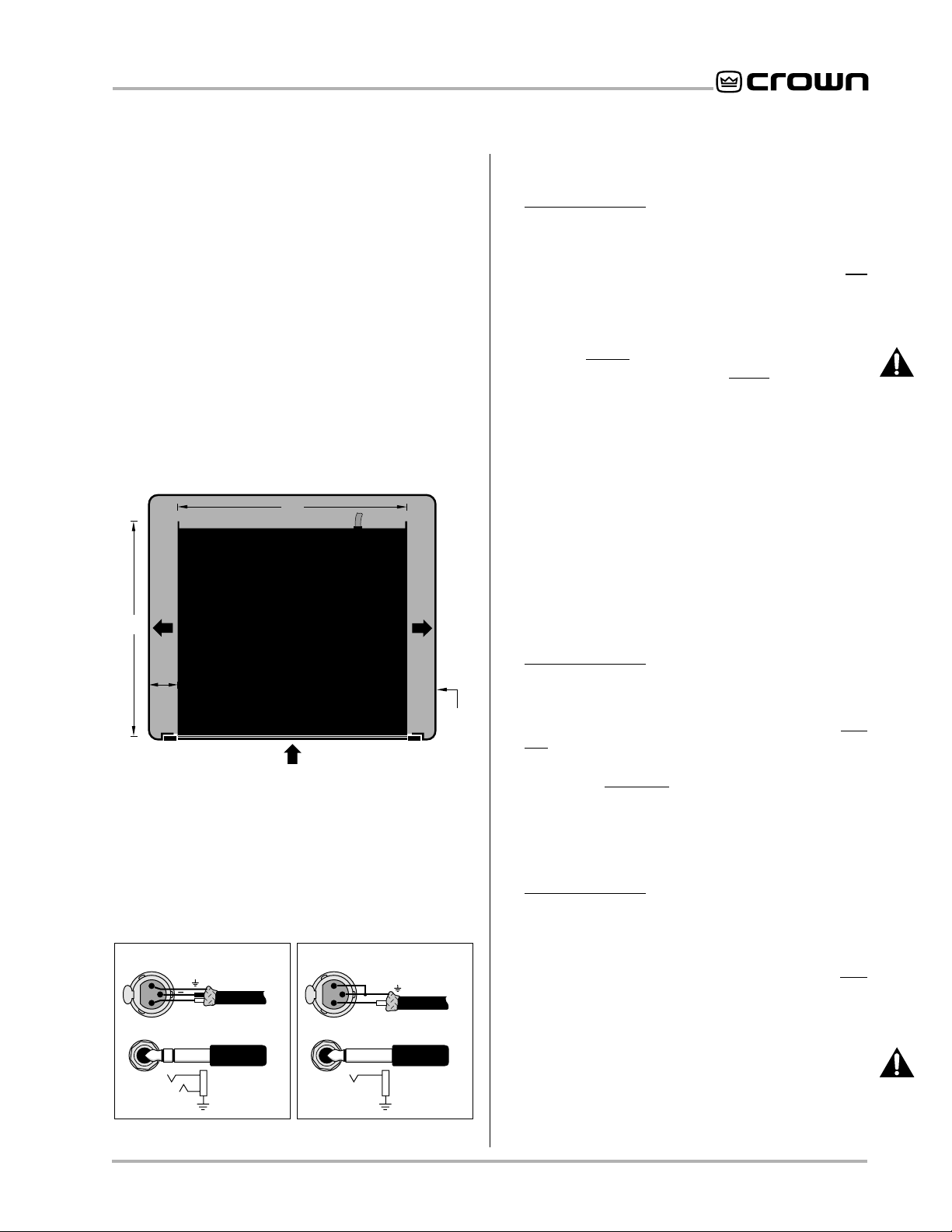
Power Base Series Power Amplifiers
2 Installation
Always remove power from the unit and turn the level
controls off (fully counterclockwise) when making or
breaking connections. This reduces the chance of
blasts that can cause loudspeaker damage.
The guidelines below are provided to help you quickly
get your amplifier installed and ready to go. Be sure to
follow the instructions in Sections 2.1 and 2.2 for the
selected mode of operation. Additional information on
input sensitivity, load protection and required AC
mains is provided in Sections 2.3, 2.4 and 2.5.
1. Install the amplifier in a standard 19 inch (48.3 cm) rack
or place it on a stable surface. The mounting dimensions
are 19 inches (48.3 cm) wide, 3.5 inches (8.9 cm) tall
and 16 inches (40.6 cm) deep behind the mounting surface. IMPORTANT! Allow for adequate ventilation.
17 in
43.2 cm
IMPORTANT: Be sure the back of
the amplifier is supported.
AIR
FLOW
16 in
40.6 cm
2 in
MIN.
AMPLIFIER
(TOP VIEW)
AIR FLOW
Fig. 2.2 Do NOT Block Air Flow
2. Use high-quality loudspeaker cables to connect the load
to the amplifier’s outputs. Do not use shielded cable.
3. Use shielded cables to connect audio sources to the
amplifier inputs. Either balanced or unbalanced wiring
can be used as shown below. (XLR connectors are available with the MT-XLR accessory. See Section 5.)
1
2
INPUT
3
+
BALANCED
GND
–
+
PREAMPLIFIER
–
SHIELD
FROM
UNBALANCED
1
3
2
+
INPUT
+
SHIELD
SHIELD
PREAMPLIFIER
AIR
FLOW
FROM
RACK
CABINET
2.1 Stereo
1. Turn down the level controls (fully counterclockwise) and
turn off the amplifier.
2. Set the back panel stereo/mono switch to Stereo.
3. If present, remove the Parallel-Mono jumper.
4. Connect the input and output cables as shown in the first
example in Figure 2.1.
5. Turn on the amplifier and adjust the level for each channel using the back panel level controls.
CAUTION: Never parallel the two outputs by directly tying them together, and never parallel them
with the output of another amplifier.
2.2 Mono
Your amplifier’s mono modes provide double the
power of Stereo mode in a single channel. In BridgeMono mode, the outputs are wired in series for twice
the output voltage. In Parallel-Mono mode, the outputs
are paralleled for twice the current capacity.
Bridge-Mono mode is provided for loads with an impedance greater than 4 ohms. Parallel-Mono mode
should be used with loads of 4 ohms or less.
B R I D G E - M O N O
1. Turn down the level controls (fully counterclockwise) and
turn off the amplifier.
2. Set the back panel stereo/mono switch to Bridge-Mono.
3. If present, remove the Parallel-Mono jumper.
4. Connect the input and output cables as shown in the second example in Figure 2.1. Only use the channel 1 input.
5. Make sure the load is balanced (neither side shorted to
ground) and do not use the black (–) binding posts.
6. Turn on the amplifier and adjust the level. Only use the
channel 1 level control.
P A R A L L E L - M O N O
1. Turn down the level controls (fully counterclockwise) and
turn off the amplifier.
2. Set the back panel stereo/mono switch to Parallel-Mono.
3. Install a solid, 14-gauge (2 mm2) or heavier jumper wire
across the two red (+) binding post outputs.
4. Connect the input and output cables as shown in the third
example in Figure 2.1. Only use the channel 1 input.
5. Turn on the amplifier and adjust the level. Only use the
channel 1 level control.
CAUTION: With Parallel-Mono wiring, do not switch
to Stereo or Bridge-Mono mode until the output
jumper wire is removed.
Fig. 2.3 Power Base Input Wiring
Page 9
Page 46

Power Base Series Power Amplifiers
2.3 Input Sensitivity Adjustment
The input sensitivity switch inside the amplifier is set to
0.775 volts at the factory. It can be changed to 1.4 volts
or a voltage gain of 26 dB as follows:
1. Turn off and unplug the amplifier from the AC source.
2. Remove the access cover on the back panel.
3. Locate the labeled access hole for the sensitivity switch.
4. Set the switch to the desired position.
5. Replace the access cover plate.
CH-1
567
4
3
2
1
0
GAIN
®
requires a
8
9
UNBALANCED
10
INPUT WIRING
11
12
GND
+
SLEEVE
TIP
When set to 26 dB gain, the
2.0 volt input, the
put and the
Power Base-2
Power Base-3
Power Base-1
®
requires a 2.5 volt in-
™
requires a 3.2 volt input to
deliver full output into an 8 ohm load.
SENSITIVITY SWITCH INSIDE ACCESS HOLE
1.4 V
26 dB
THIS AMPLIFIER IS EQUIPPED WITH SELECTABLE INPUT SENSITIVITY. REMOVE COVER PLATE (ABOVE) TO ACCESS SENSITIVITY SWITCH.
BALANCED
INPUT WIRING
+
TIP
RING
–
SLEEVE
GND
CH-2
567
4
8
9
3
10
2
1
11
0
12
GAIN
Fig. 2.4 Input Sensitivity Switch
0.77 V
INPUT
INPUT GROUND LIFT
LIFT
(AFFECTS PHONE INPUTS ONLY.)
INPUT
(MONO)
Example: (A) Find the peak music power of your loudspeaker
(such as 75 watts). (B) Find the loudspeaker impedance (8
ohms). (C) Draw a line between points A and B. The line intersects the middle scale at the correct fuse value (1.5 amps).
1.0
1.2
1.4
1.6
2
2.5
3
4
5
6
Example:
7
8
9
10
12
14
16
20
25
30
40
Impedance = 8 ohms.
Peak Power = 75 W
Answer: Fuse = 1.5 A
(ohms)
LOUDSPEAKER IMPEDANCE
FUSE
(amps)
20
15
10
8
6
5
4
3
2
1.5
1
.8
.6
.5
.4
.3
.2
.15
.1
.08
3000
2000
1500
1000
800
600
400
300
200
150
100
80
60
40
30
20
15
10
8
6
4
3
LOUDSPEAKER RATING
PEAK MUSIC POWER
2
1.5
1
(Typically 4 times the continuous average power)
(watts)
2.4 Additional Load Protection
To protect against excessive power, a fuse can be
added in series with each loudspeaker cable. A single
fuse can protect the entire system, or one can be used
for each driver. High-frequency drivers (tweeters) are
usually more sensitive to large voltage peaks, while
low-frequency drivers (woofers) are typically most sensitive to the heat from average (RMS) output power. To
protect your tweeters, we recommend that you use a
high-speed instrument fuse like the Littlefuse 361000
series. To protect your woofers, we recommend using a
slow-blow fuse that more closely represents the thermal
response of your woofer. Use Figure 2.5 to find the correct value for either type of fuse.
Page 10
Fig. 2.5 Loudspeaker Fuse Nomograph
2.5 Required AC Mains
All
Power Base
priate line cord and plug. When possible, use a power
receptacle on a dedicated circuit, and always make
sure it will provide the right voltage and sufficient current. We do not recommend operating your amplifier
with voltages greater than 10% above or below the
unit’s rated voltage. For example, if your amplifier is
rated for 120 VAC, the line voltage should not exceed
132 VAC.
amplifiers are shipped with an appro-
Page 47

Power Base Series Power Amplifiers
3 Operation
3.1 Precautions
Although your amplifier is protected from external faults,
the following safety precautions are recommended:
1. There are important differences among the Stereo,
Bridge-Mono and Parallel-Mono operating modes.
Please refer to Sections 2 for additional information.
2. WARNING: Do not change the position of the
stereo/mono switch unless the amplifier is first
turned off.
3. CAUTION: In Parallel-Mono mode, a jumper is
used to connect the red binding post outputs.
Be sure to remove this jumper for Bridge-Mono
or Stereo mode, or high distortion and excessive
heating will occur. Also, make sure the stereo/
mono switch is set to the proper position.
4. Use care when making connections, selecting signal sources and controlling the output level. The
load you save may be your own!
5. Do not short the ground lead of an output cable to
the input signal ground. This will form a ground loop
and may cause oscillations.
6. Operate the amplifier from AC mains of not more
than 10% variation above or below the selected line
voltage and only at the specified line frequency.
7. Never connect the output to a power supply output, battery or power main. Such connections
may result in electrical shock.
8. Tampering with the circuitry by unqualified personnel or making unauthorized circuit changes may be
hazardous and invalidates all agency listings.
Remember: Crown is not liable for any damage that results from overdriving other system components.
3.2 Power Indicator
When lit, the amber power indicator (to the left of the
power switch) shows that the amplifier has been turned
on. It is driven only by the low-voltage power supply
and does not indicate the status of the high-voltage
supplies.
3.3 Protection Systems
Power Base
tems, including
protection, transformer thermal protection and fuses or
circuit breakers that protect the power supplies.
amplifiers have extensive protection sys-
ODEP
, ultrasonic/RF protection, drive
3.3.1
ODEP
Crown invented
under demanding conditions and to increase output
efficiency. To do this, Crown established a rigorous program to measure each transistor’s
(SOA). Intelligent circuitry was then designed to simulate the instantaneous conditions of the output transistors. Its name describes what it does: Output Device
Emulation Protection, or
compares transistor conditions to their known SOA. If
more power will be asked of them than they can deliver
under the existing conditions,
until conditions fall within the SOA. Limiting is proportional and kept to an absolute minimum—only what is
required to prevent output transistor damage. Under
normal conditions, no limiting is required and
transparent to the audio signal.
ODEP
makes possible a quantum leap in output effi-
ciency and reliability—with
3.3.2 Ultrasonic and Radio Frequency Protection
An amplifier’s slew rate only needs to be large enough
to deliver the maximum voltage at the highest required
frequency. Higher slew rates actually allow undesirable
ultrasonic and radio frequencies to be reproduced. By
design,
rate to limit the highest frequencies that they reproduce.
Limiting occurs well above 20 kHz so there is no audible effect on performance. This approach protects
the amplifier from radio frequencies and can even protect some sensitive loads (including some tweeters).
3.3.3 Drive Protection
The drive protection system temporarily removes output
drive to protect the amplifier and its loads. Drive protection can be activated in two situations. First, if dangerous
subsonic frequencies or direct current (DC) is detected
in the amplifier’s output, the unit will activate its DC/lowfrequency protection circuitry which puts the amplifier in
drive protection mode. This protects the loads and prevents oscillations. The unit resumes normal operation as
soon as the amplifier no longer detects dangerous output. Although it is extremely unlikely that you will ever
activate the amplifier’s DC/low frequency protection
system, improper source materials like subsonic square
waves or input overloads that excessively clip the input
signal can activate this system.
The amplifier’s fault protection system will put the amplifier in drive protection mode in rare situations where
heavy common-mode current is detected in the output.
Power Base
ODEP
to keep the amplifier working
safe operating area
ODEP
. In simple terms,
ODEP
limits the drive
ODEP
, the show goes on.
amplifiers have a controlled slew
ODEP
ODEP
is
Page 11
Page 48

Power Base Series Power Amplifiers
The unit should never output heavy common-mode current unless its circuitry is damaged. Activating drive
protection helps prevent further damage.
3.3.4 Transformer Thermal Protection
All
Power Base
amplifiers have transformer thermal
protection. This protection circuitry is activated in unusual situations where the unit’s transformer temperature rises to unsafe levels. Under these abnormal
conditions, the unit removes power to the high-voltage
transformer. The fan will continue to run in all units except those with 220/240 VAC transformers. The amplifier will return to normal after it cools to a safe
temperature.
It is very unlikely that your
Power Base
amplifier will
ever activate transformer thermal protection as long as
it is operated within rated conditions. Your amplifier is
designed to continue operating under conditions
where other amplifiers would fail. But even when you
exceed the limits of a
Power Base
amplifier, it still pro-
tects itself—and your investment—from damage.
3.3.5 Fuses and Circuit Breakers
All 120 VAC, 60 Hz units and all
Power Base-3
units
have a fuse that protects the low-voltage power supply
and cooling fan. The
Power Base-1
and
Power Base-2
high-voltage power supplies are protected by fuses,
while the
Power Base-3
high-voltage power supplies
are protected by a circuit breaker. With rated loads
and output levels, these fuses (or the circuit breaker)
should only shut down the amplifier in the incredibly
rare instance of a catastrophic amplifier failure. The
ODEP
protection system keeps the amplifier operational under most other severe conditions. The fuses
(or breaker) can also shut down the amplifier in situations where extremely low-impedance loads and high
output levels result in excessive current draw.
A
Power Base
amplifier will not blow its fuses or trip its
breaker unless something is wrong. In the rare event
that an internal fuse blows, please refer the unit to a
qualified technician. If the breaker in a
Power Base-3
trips, try to identify and correct the problem before resetting it with the back panel Circuit Breaker Reset. If
the problem persists, refer the unit to a qualified technician.
3.4 Controls
The Power switch is th only control located on the front
panel. All others are located on the rear, including the
level controls.
When making any setup or wiring changes, don’t forget
to turn off the amplifier, turn down the level controls and
disconnect the power cord. Be sure to turn down (full
counterclockwise) the channel 2 level control when using either mono mode. The Parallell Mono/Stereo/
Bridge Mono switch is used to select Stereo, BridgeMono or Parallel-Mono operating modes. The Input
Ground Lift switch isolates the phone jack input
grounds from the chassis ground to help prevent
ground loops. It does not affect any installed input accessories. The Input Sensitivity Switch, located inside
the back cover plate, sets the amplifier’s input sensitivity (refer to subsection 2.3 for information on changing
this switch). And the
Power Base-3
has a back panel
Circuit Breaker Reset button that resets the circuit
breaker (refer to subsection 3.3.5).
CHANNEL 2
LEVEL CONTROL
CH-2
567
4
8
9
3
10
2
1
11
0
12
GAIN
INPUT GROUND LIFT
INPUT
LIFT
(AFFECTS PHONE INPUTS ONLY.)
INPUT
(MONO)
Fig. 3.1 Back Panel Level Controls
CHANNEL 1
LEVEL CONTROL
CH-1
567
4
8
3
2
1
11
0
12
GAIN
9
10
3.5 Filter Cleaning
A dust filter is provided on the unit’s air intake. If it becomes clogged, the unit will cool less efficiently and
may produce lower output levels. To clean the filter,
use a phillips screwdriver to remove the three screws
the secure the front grille. Use mild dishwashing detergent and warm water for best cleaning results. Be sure
the filter is dry before you reinstall it. Replacement filters may be ordered from the factory.
Dust filters are not 100% efficient—long term this may
require internal heat-sink cleaning by a qualified technician. Internal cleaning information is available from
our Technical Support Group.
Page 12
Page 49

Power Base Series Power Amplifiers
4 Specifications
All specifications apply to units in Stereo mode with 8-ohm loads
and an input sensitivity of 26 dB unless otherwise specified.
Standard 1 kHz Power: refers to maximum average power in
watts at 1 kHz with 0.1% THD+ noise.
Full Bandwidth Power: refers to maximum average power in
watts from 20 Hz to 20 kHz with 0.1% THD+ noise.
120 VAC, 60 Hz Units: refers to amplifiers with dedicated transformers for 120 VAC, 60 Hz power mains.
Performance
Frequency Response: ±0.1 dB from 20 Hz to 20 kHz
at 1 watt.
Phase Response: ±10 degrees from 10 Hz to 20 kHz
at 1 watt.
Signal-to-Noise: A-weighted, better than 105 dB below full bandwidth power. Better than 100 dB below full
bandwidth power from 20 Hz to 20 kHz.
Total Harmonic Distortion (THD): Less than 0.05%
at full bandwidth power from 20 Hz to 1 kHz increasing linearly to 0.1% at 20 kHz.
Intermodulation Distortion (IMD): (60 Hz and 7 kHz
4:1) Less than 0.05% from less than 158 milliwatts to full
bandwidth power.
Damping Factor: Greater than 1,000 from 10 Hz to 400 Hz.
Crosstalk
Power Base-1
width power from 50 Hz to 2 kHz, rising linearly to
greater than 60 dB at 20 kHz.
Power Base-2
width power from 50 Hz to 2 kHz, rising linearly to
greater than 66 dB at 20 kHz.
Power Base-3
width power from 50 Hz to 4 kHz, rising linearly to
greater than 70 dB at 20 kHz.
Common Mode Rejection (CMR): Better than 70 dB
below rated full bandwidth power from 20 Hz to 1 kHz
falling linearly to better than 50 dB at 20 kHz.
Controlled Slew Rate: Greater than 13 volts/ms.
Voltage Gain: 20:1 ±3% or 26 dB ±0.25 dB at the maxi-
mum level setting (Input Sensitivity switch set to its 26
dB position).
Power Base-1
volt sensitivity; 28:1 ±12% or 29.1 dB ±1 dB at 1.4 volt
sensitivity.
: Greater than 75 dB below full band-
: Greater than 90 dB below full band-
: Greater than 90 dB below full band-
: 51:1 ±12% or 34.3 dB ±1 dB at 0.775
Power Base-2
: 64:1 ±12% or 36.2 dB ±1 dB at 0.775
volt sensitivity; 35:1 ±12% or 31.0 dB ±1 dB at 1.4 volt
sensitivity.
Power Base-3
: 83:1 ±12% or 38.4 dB ±1 dB at 0.775
volt sensitivity; 46:1 ±12% or 33.3 dB ±1 dB at 1.4 volt
sensitivity.
Power
Output Power:
teed minimums for standard 1 kHz power. For more information, see the power matrices in Figures 4.1 through 4.6
(maximum average power @ 0.1% THD + N).
Power Base-1
Stereo mode (both channels driven):
Bridge-Mono mode:
Parallel-Mono mode:
Power Base-2
Stereo mode (both channels driven):
Bridge-Mono mode:
Parallel-Mono mode:
Power Base-3
Stereo mode (both channels driven):
Bridge-Mono mode:
1525 watts into 8 ohms.
1090 watts into 16 ohms.
Parallel-Mono mode:
1530 watts into 2 ohms.
1080 watts into 4 ohms.
Load Impedance: Safe with all types of loads. Rated
for 4 to 8 ohms in Stereo, 8 to 16 ohms in BridgeMono and 2 to 4 ohms in Parallel-Mono mode.
The following specifications are guaran-
240 watts into 4 ohms.
200 watts into 8 ohms.
455 watts into 8 ohms.
395 watts into 16 ohms.
455 watts into 2 ohms.
400 watts into 4 ohms.
460 watts into 4 ohms.
325 watts into 8 ohms.
910 watts into 8 ohms.
660 watts into 16 ohms.
920 watts into 2 ohms.
655 watts into 4 ohms.
760 watts into 4 ohms.
540 watts into 8 ohms.
Page 13
Page 50

Power Base Series Power Amplifiers
Required AC Mains: Current, frequency and voltage
requirements are provided on each unit’s back panel.
All models draw 90 watts or less at idle.
Power Base-1
Power Base-2
Power Base-3
Low-Voltage Power Supply: A ±24 VDC fanformer
supply (fan motor winding) regulated to ±15 VDC.
AC Connector: An appropriate AC line cord and plug
are provided. 120 VAC, 60 Hz units have a standard
3-wire, 15-amp grounded connector (NEMA 5-15P).
: Draws up to 6 amps of current.
: Draws up to 10 amps of current.
: Draws up to 15 amps of current.
Controls
Power: A front panel rocker switch used to turn the
amplifier on and off.
Level: A back panel rotary potentiometer for each channel used to control the output level.
Stereo/Mono: A three-position back panel switch used
to select Stereo, Bridge-Mono or Parallel-Mono mode.
Sensitivity: A three-position switch inside the back
cover plate used to select the input sensitivity for both
channels: 0.775 volts or 1.4 volts for standard 1 kHz
power, or 26 dB voltage gain (see Section 2.3).
Input Ground Lift: A two-position back panel switch
used to isolate the phone jack and chassis grounds.
Reset (
ton used to reset the circuit breaker that protects the
power supplies.
Power Base-3
only): A back panel push but-
Indicators
Power: This amber indicator shows the on/off status of
the low voltage power supply.
Input/Output
Input Connector: Balanced ¼ inch phone jacks. See
Section 5 for XLR and barrier block accessories.
Input Impedance: Nominally 20 K ohms, balanced;
10 K ohms, unbalanced.
Output Connector: Two sets of color-coded 5-way bbinding
posts (for banana plugs, spade lugs or bare wire).
Output Impedance: Less than 10 milliohms in series
with less than 2 microhenries.
DC Output Offset: Less than 10 millivolts.
Output Signal
Stereo: Unbalanced, two-channel.
Bridge-Mono: Balanced, single-channel. Channel 1
controls are active; Channel 2 controls should be
turned down and not used.
Parallel-Mono: Unbalanced, single-channel. Channel
1 controls are active; Channel 2 controls should be
turned down and not used.
Protection
Power Base
open or mismatched loads; overloaded power supplies;
excessive temperature, chain destruction phenomena,
input overload and high-frequency blowups. They also
protect loudspeakers from input and output DC, as well
as providing protection from turn-on/turn-off transients.
If operating conditions are unreasonable, the patented
ODEP
tect the output transistors, particularly in the case of elevated temperature. A thermal switch imbedded in the
transformer protects the power supplies from overload.
In the rare event that a transformer overheats, the thermal switch removes power, waits until the unit has cooled
to a safe temperature and then resets itself.
Turn On: Four second delay with no dangerous transients. Contact us if you need to change the delay.
amplifiers are protected against shorted,
circuitry proportionally limits the drive level to pro-
Construction
Durable black finish on steel chassis with special “flowthrough” ventilation from front to side panels.
Cooling: Internal heat sinks with forced-air cooling
for rapid, uniform heat dissipation.
Dimensions: Standard 19-inch (48.3 cm) rack mount
width (EIA RS-310-B), 3.5-inch (8.9 cm) height and
16-inch (40.6 cm) depth behind the mounting surface.
Approximate Weight: Center of gravity is 6 inches
(15.2 cm) behind front mounting surface.
120 VAC, 60 Hz Units:
Power Base-1
(15.4 kg) shipping weight.
Power Base-2
(17.2 kg) shipping weight.
Power Base-3
(18.2 kg) shipping weight.
: 30 pounds (13.6 kg) net; 34 pounds
: 34 pounds (15.4 kg) net; 38 pounds
: 36 pounds (16.3 kg) net; 40 pounds
Page 14
Page 51

Power Base Series Power Amplifiers
Crown specifications are guaranteed for three years.
In an effort to provide you with as much information as possible about the high power-producing capabilities of your amplifier, we have
created the following power matrices.
Minimum Power Specifications
Crown’s minimum power specifications represent the absolute smallest amount of output power you can expect from your amplifier when it
is driven to full output under the given conditions. Some spaces in each matrix may be left blank because the same guarantee is not
provided for those conditions—however, your amplifier will perform well under all conditions listed in each matrix.
When measuring power, 0.1% THD appears to be the industry standard for distortion. Two of the maximum average power specifications
shown in each minimum power matrix are measured at 0.1% THD so you can easily compare Crown specifications to those of other manufacturers. But this high level of distortion actually allows for some clipping which is undesirable. Because of this, a maximum average power
spec at 0.05% THD is included in each minimum power matrix which represents non-clipped conditions. Although most manufacturers do
not give you power specifications at 0.05% THD, we encourage them to provide these specifications so you will have a more realistic
representation of the way amplifiers should be used in the real world—without a clipped output signal.
Many manufacturers publish power specs with a tolerance of ±1 dB or worse. This means their amplifier can deviate more than 20% in
output! A 100 watt amplifier would meet their specification if it only produced 79.4 watts. Other manufacturers qualify their specs by saying
they are “typical,” “subject to manufacturing tolerances,” “single channel driven” or that they are specified with “fuses bypassed.” Each of
these statements effectively removes any performance guarantee. In fact, some manufacturers use these tactics to generate large power
numbers, and they don’t even print a disclaimer. We take a different approach at Crown—our amplifiers are
their specifications for three years. Further, because our published specs are set below our “in-house” measurements, you can expect
Crown amplifier to
Minimum Power Notes:
All minimum power specifications are based on 0.1% regulated AC mains and an ambient room temperature of 70° F (21° C). A 100V, 50Hz model was used
because of its higher current demand. The standard EIA power measurement (RS-490) is not identified here because it is identical to the FTC Continuous
Average Power specification.
1. A 1 kHz sine wave is presented to the amplifier and the output monitored for nonlinear distortion. The level is increased until the THD reaches 0.1%. At this level
the average power per channel is reported.
2. A sine wave is presented to the amplifier over the range from 20 Hz to 20 kHz and the output monitored for nonlinear distortion. The level at each frequency is
increased until the THD reaches 0.1%. At this level the average power per channel is reported.
3. A 1 kHz sine wave is presented to the amplifier and the output monitored for nonlinear distortion. The level is increased until the THD reaches 0.05%. At this
level the average power per channel is reported.
4. Continuous power in the context of Federal Trade Commission testing is understood to be a minimum of five minutes of operation. Harmonic distortion is
measured as the RMS sum total and given as a percentage of the fundamental output voltage. This applies for all wattages greater than 0.25 watts.
exceed
its published minimum power specs. We believe you should get what you pay for.
guaranteed
to meet or exceed
every
Power Base-1 – Minimum Guaranteed Power (Watts)
Stereo-Mono
Mode
AC Mains120 VAC, 60 Hz Units
Stereo
(both channels
driven)
Bridge-Mono
(balanced output)
Parallel-Mono
Stereo
(both channels
driven)
Bridge-Mono
(balanced output)
International Units
Parallel-Mono
Fig. 4.1 Power Base-1 Minimum Power Matrix
0.1% THD+N
(See note 1)
Load (Ohms)
4
8
8
16
2
4
4
8
8
16
2
4
Maximum Average
1 kHz
240
200
455
395
455
400
230
205
465
410
440
410
0.1% THD+N
(See note 2)
20Hz-20kHz
175
185
360
370
165
185
355
375
0.05% THD+N
(See note 3)
1 kHz
235
200
455
390
445
395
225
200
455
405
430
405
FTC Continuous Average
0.1% THD + Noise
(See note 4)
1 kHz 20Hz-20kHz
200
390
390
200
390
390
180
350
175
350
Page 15
Page 52

Power Base Series Power Amplifiers
Power Base-2 –
Stereo-Mono
Mode
AC Mains120 VAC, 60 Hz Units
Stereo
(both channels
driven)
Bridge-Mono
(balanced output)
Parallel-Mono
Stereo
(both channels
driven)
Bridge-Mono
(balanced output)
International Units
Parallel-Mono
Fig. 4.2 Power Base-2 Minimum Power Matrix
0.1% THD+N
(See note 1)
Load (Ohms)
4
8
8
16
2
4
4
8
8
16
2
4
Minimum Guaranteed Power (Watts)
Maximum Average
1 kHz
460
325
910
660
920
655
425
310
855
620
850
620
0.1% THD+N
(See note 2)
20Hz-20kHz
425
310
830
615
390
290
775
575
0.05% THD+N
(See note 3)
1 kHz
460
325
905
655
915
650
425
305
850
615
845
615
FTC Continuous Average
0.1% THD + Noise
(See note 4)
1 kHz 20Hz-20kHz
385
310
815
625
805
630
395
305
790
615
785
610
265
530
325
275
640
545
Power Base-3 –
Stereo-Mono
Mode
AC Mains120 VAC, 60 Hz Units
Stereo
(both channels
driven)
Bridge-Mono
(balanced output)
Parallel-Mono
Stereo
(both channels
driven)
Bridge-Mono
(balanced output)
International Units
Parallel-Mono
Fig. 4.3 Power Base-3 Minimum Power Matrix
0.1% THD+N
(See note 1)
Load (Ohms)
4
8
8
16
2
4
4
8
8
16
2
4
Minimum Guaranteed Power (Watts)
Maximum Average
1 kHz
760
540
1525
1090
1530
1080
680
510
1335
1025
1365
1015
0.1% THD+N
(See note 2)
20Hz-20kHz
715
525
1430
1045
630
495
1240
980
0.05% THD+N
(See note 3)
1 kHz
755
540
1500
1075
1520
1080
660
505
1305
1000
1340
1010
FTC Continuous Average
0.1% THD + Noise
(See note 4)
1 kHz 20Hz-20kHz
530
1055
1065
555
510
1115
1025
1115
1030
495
985
485
470
1085
930
Page 16
Page 53

Power Base Series Power Amplifiers
Maximum Power Specifications
Crown’s maximum power specifications represent the largest amount of output power you can expect from your amplifier when it is driven to
full output under the given conditions. These specifications can be used to prevent loudspeaker and hearing damage.
The maximum power matrices include specifications for single cycle and 40 millisecond burst sine waves. Burst signals act like large
transient peaks that are present in common source signals. Loudspeakers can respond to a single cycle burst, so the single cycle burst
specifications should be used to help you protect your loudspeakers. In contrast, a 40 millisecond burst represents the typical response time
of the human ear. Your ear will not respond to the entire dynamic change of a burst that lasts less than 40 milliseconds.
The specifications are provided at 0.05% THD because this represents a low distortion condition. To help you operate your amplifier within
these tolerances, Crown’s premium amplifiers include an input/output comparator that shows when the amplifier has exceeded 0.05% THD.
Operating the amplifier at levels higher than 0.05% THD can result in output power levels that are higher than those listed in the maximum
power matrices.
Maximum Power Notes:
All maximum power specifications are based on 0.1% regulated AC mains and an ambient room temperature of 70° F (21° C). A 100V, 50Hz model was used
because of its higher current demand. Although it is an unusual condition, your amplifier can function well with AC mains voltages up to 10% over the specified
line voltage. With overvoltage conditions, your amplifier may be capable of delivering instantaneous power levels up to 20% greater than the specifications in the
matrix.
1. A single cycle sine wave is presented to the amplifier and monitored for nonlinear distortion. The average power during the burst is reported. Loudspeakers
must be able to withstand this level if they are to be safely used with this amplifier.
2. A 40 millisecond sine wave burst (10 percent duty cycle) is presented to the amplifier and monitored for nonlinear distortion. The average power during the
burst is reported. This power level is a measurement of the amplifier’s maximum transient power that can be perceived by the human ear.
Stereo-Mono
Mode
AC Mains120 VAC, 60 Hz Units
Stereo
(both channels
driven)
Bridge-Mono
(balanced output)
Parallel-Mono
Stereo
(both channels
driven)
Bridge-Mono
(balanced output)
International Units
Parallel-Mono
Fig. 4.4 Power Base-1 Maximum Power Matrix
Load (Ohms)
4
8
8
16
2
4
4
8
8
16
2
4
Power Base-1 –
Single Cycle Tone Burst
At less than 0.05% THD
(See note 1)
50 Hz
325
265
630
540
635
530
325
290
640
580
620
580
1 kHz
335
310
640
630
645
615
330
345
650
690
625
690
Maximum Power (Watts)
40 Millisecond Tone Burst
0.05% THD + Noise
(See note 2)
7 kHz 50 Hz
335
300
620
610
640
600
330
335
670
670
625
670
315
230
600
470
620
465
320
260
635
520
615
515
1 kHz 7 kHz
295
220
565
440
580
430
315
235
625
470
615
475
310
230
580
455
605
450
330
250
655
495
625
490
Page 17
Page 54

Power Base Series Power Amplifiers
Stereo-Mono
Mode
AC Mains120 VAC, 60 Hz Units
Stereo
(both channels
driven)
Bridge-Mono
(balanced output)
Parallel-Mono
Stereo
(both channels
driven)
Bridge-Mono
(balanced output)
International Units
Parallel-Mono
Power Base-2 –
Single Cycle Tone Burst
At less than 0.05% THD
(See note 1)
Load (Ohms)
50 Hz
655
4
460
8
1410
8
915
16
1440
2
915
4
4
720
8
465
8
1440
16
920
2
1390
4
915
Maximum Power (Watts)
1 kHz
805
525
1850
1060
1685
1055
900
530
1770
1055
1670
1055
7 kHz 50 Hz
790
515
1805
1020
1645
1020
885
510
1785
1020
1655
1015
40 Millisecond Tone Burst
0.05% THD + Noise
(See note 2)
550
400
1190
795
1185
805
605
410
1200
820
1185
820
Fig. 4.5 Power Base-2 Maximum Power Matrix
1 kHz 7 kHz
500
375
1090
755
1085
750
545
380
1075
750
1065
750
520
395
1125
780
1120
775
565
395
1120
785
1110
775
Stereo-Mono
Mode
AC Mains120 VAC, 60 Hz Units
Stereo
(both channels
driven)
Bridge-Mono
(balanced output)
Parallel-Mono
Stereo
(both channels
driven)
Bridge-Mono
(balanced output)
International Units
Parallel-Mono
Power Base-3 –
Single Cycle Tone Burst
Load (Ohms)
50 Hz
1090
4
715
8
2155
8
1415
16
2140
2
1420
4
4
1190
8
785
8
2355
16
1540
2
2330
4
1570
At less than 0.05% THD
(See note 1)
Maximum Power (Watts)
1 kHz
1575
870
3140
1740
3135
1735
1750
960
3490
1915
3485
1895
7 kHz 50 Hz
1525
838
3040
1675
3015
1665
1695
920
3380
1840
3345
1825
40 Millisecond Tone Burst
0.05% THD + Noise
(See note 2)
910
610
1780
1250
1790
1225
970
675
1945
1360
1940
1360
Fig. 4.6 Power Base-3 Maximum Power Matrix
1 kHz 7 kHz
815
570
1615
1135
1605
1135
870
625
1725
1235
1720
1235
855
595
1690
1180
1680
1170
920
645
1805
1285
1800
1270
Page 18
Page 55

Power Base Series Power Amplifiers
5 Accessories
There are two accessories available at the time of this
printing: the
MT-XLR
Factory Service Center or the Crown factory.
5.1 MT-XLR
The
MT-XLR
standard 3-pin female XLR input connectors. The
MT-XLR
connections in a system that uses standard XLR connectors. It can also be used in systems that need to
daisy chain an input signal from one amplifier to an-
MT-XLR
and
MT-BB
and the
MT-BB
. Important: The
must be installed at a Crown
is an accessory panel that provides two
accessory makes it easy to quickly change
other. Because the
MT-XLR
connectors are wired in
parallel with the amplifier’s built in phone jack connectors, an input signal fed to either input can be fed to
another amplifier from the unused connector for that
channel.
5.2 MT-BB
The
MT-BB
is an accessory panel that provides barrier
strip input connectors. An
desirable in applications requiring bare wire connections. It can also be used to daisy chain an input signal
from one amplifier to another just like the
MT-BB
accessory might be
MT-XLR
.
MT-XLR
CH-2 INPUT CH-1 INPUT
PUSHPUSH
THESE XLR INPUTS ARE CONNECTED IN PARALLEL WITH THE PHONE JACK INPUTS.
Fig. 5.1 The MT-XLR
MT-BB
3
GND
12
CH-2 INPUT CH-1 INPUT
Fig. 5.2 The MT-BB
– +– +
Page 19
Page 56

Page 57

Page 58

Page 59

Page 60

 Loading...