

Crompton integra 1530, integra 1560, integra 1580 Communications Manual

Crompton
INTEGRA 1530, 1560, 1580
Communications Guide
Crompton Instruments
Freebournes Road
Witham
Essex
CM8 3AH
England
Tel: +44 (0) 1376 509 509
Fax: +44 (0) 1376 509 511
E-Mail: crompton.info@tycoelectronics.com
Integra Comms Issue 1 Jan 2006

Contents Page
1 Modbus
tm
4
1.1 Modbus tm Overview 4
1.2 Input Registers 5
1.3 Modbustm Holding Registers and Integra set up 7
1.4 Analogue Output setting via Modbus 11
2 RS485 Implementation of Johnson Controls Metasys 13
2.1 Application details 13
2.2 Metasys release requirements 13
2.3 Support for Metasys Integration 13
2.4 Support for Crompton Integra operation 13
2.5 Design considerations 13
2.6 METASYS N2 Integra Point Mapping table 14
3 Integra Profibus Interface 16
3.1 GSD file 16
3.2 Floating Point Format 16
3.3 Single Parameter access 16
3.4 Functionality of the PLC Function Block 16
3.4.1 Reading 16
3.4.2 Writing 17
3.5 Common Pro b l ems 17
4 The LonWorks Interface 18
4.1 XIF File 18
4.2 Overview and Device Functional Profile 18
4.3 Node Object 19
4.3.1 Network Variables 19
4.3.2 Object Status 19
4.3.3 Configuration Properties 19
4.4 Voltmeter Functional Profile 19
4.4.1 Voltmeter Network Variables 20
4.5 Ammeter Functional Profile 21
4.5.1 Ammeter Network Variables 21
4.5.2 Ammeter Configuration Properties 22
4.6 Energy Meter Functional Profile 23
4.6.1 Energy Meter Network Variables 23
4.6.2 Energy Meter Configuration Properties 23
4.7 Power Meter Functional Profile 25
4.7.1 Power Meter Network Variables 25
4.7.2 Power Meter Configuration Properties 26
4.8 Demand Ammeter Functional Profile 27
2 Integra Comms Issue 1 Jan 2006

Contents Page
4.8.1 Demand Ammeter Network Variables 27
4.8.2 Demand Ammeter Configuration Properties 27
4.9 Demand Power Meter Functional Profile 28
4.9.1 Demand Power Meter Network Variables 28
4.9.2 Demand Power Meter Configuration Properties 29
4.10 Power Quality Meter 30
4.10.1 Power Quality Network Variables 30
4.10.2 Power Quality Meter Configuration Properties 31
4.11 Common Pro b l ems 31
Integra Comms Issue 1 Jan 2006 3

1 Modbus
1.1 Modbus tm Overview
This section pr ovides basic info rmation for interfacing the Integra to a Modbus
information or more details of the Integra implementation is required please refer to our “Guide to RS485
Communications and the Modbus
supplier.
Integra offers the option of an RS485 communication facility for direct connection to SCADA or other
communications systems using the Modbus
format for the master's query by placing into it the device address, a function code defining the requested
action, any data to be sent, and an error check ing fie ld . The slave's re spon se me ssage is also
constructed using Modbus
returned, an d an error-checking field. If an er r or occurs in receipt of the message, Integra will ma ke no
response. If the I ntegra is unable to p erform the requested action, it will constr uct an error message and
send it as it’s response.
The electrical interface is 2-wire RS485, via 3 screw terminals. Connection should be made using twisted
pair screened cable (Typically 22 gauge Belden 8761 or equivalent). All "A" and "B" connections are
daisy chained together. The screens should also be connected to th e “Gnd” terminal. To avoid the
possibility of loop currents, an Earth connection should be made at only one point on t he network.
Line topology may or may not require terminating loads depending on the type and leng th of cable used.
Loop (ring) topology does not require any termination load.
The impedance of the termination load should match the impedance of the cable and be at both ends of
the line. The ca ble should be terminated at each end with a 120 ohm (0.25 Watt min.) resistor.
A total maximum length of 3900 feet (1200 metres) is allowed for the RS485 network. A maximum of 32
electrical nodes can be connected, including the controller.
The address of each Integra can be set to any value between 1 and 247. Broadcast mode (address 0) is
not supported .
The maximum latency time of an Integra is 150ms i. e. this is the amount of time that can pass before the
first response ch aracter is output. The supervisory programme must allow t his period of time to elapse
before assuming that the Integra is not going to respond.
The format for each byte in RTU mode is:
Coding System: 8-bit per byte
Data Format: 4 bytes (2 regist ers) per parameter.
Error Check Field: 2 byte Cyclical Redundancy Check (CRC)
Framing: 1 start bit
Data Transmission speed is selectable between 2400, 4800, 9600 and 19200 baud.
tm
tm
network. If background
tm
Protocol”, available on our CD catalogue or from any recognised
tm
RTU slave protocol. The Modb ustm protocol establishes the
tm
protocol. It contains fields confirming the action taken, any data to be
Floating point format ( to IEEE 754)
Most significant register first (Default). The default may be changed if required See Holding Reg ister "Register Order " parameter.
8 data bits, least significant bit sent first
1 bit for even/odd parity or no parity
1 stop bit if parity is used; 1 or 2 bits if no parity
4 Integra Comms Issue 1 Jan 2006

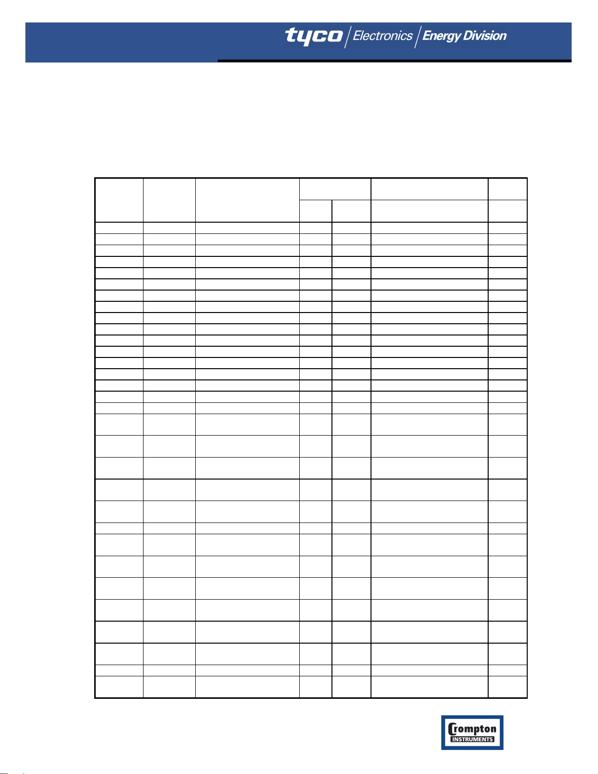
1.2 Input Registers
Input register s are used to indicate the present values of the measured an d calculated electrical
quantities.
Each parameter is held in two consecutive 16 bit registers. The following table details the 3X re gister
address, and the va lues of the address bytes within the message. A tick (√) in the column indicates that
the parameter is valid for the particular wiring system. Any parameter with a cross (X) will return the value
Zero.
Each parameter is held in the 3X registers. Modbus
.
For example, to request: Amps 1 Start address = 0006
No of registers = 0002
Amps 2 Start address = 0008
No of registers = 0002
Each request for data must be restricted to 40 parameters or less. Exceedi ng the 40 parameter limit will
cause a Modbus
tm
exception code to be returned.
tm
Function Code 04 is used to access all para meters
Integra Comms Issue 1 Jan 2006 5

–
00
02 X
–
00
04 X X
00
06
00
08 X
00
0A X X
00
0C
00
0E X X
00
10
X
00
12
00
14 X X
00
16
X
00
18
00
1A X X
00
1C
X
00
1E
00
20 X X
00
22
X
00
24
00
26 X X
00
28
X
00
2A
00
2E
00
30
00
34
00
38
00
3C
00
3E
00
42
00
46
00
48
00
4A
v
a
00
4C
00
4E
00
50
00
54
00
56
00
68
00
6A
00
C8 X X
00
CA
X
00
CC
X
00
CE X X
00
E0
00
EA
00
EC X
00
EE X X
00
F0
00
F2 X
00
F4 X X
00
F8
00
FA
-
C
00
FE
Address
(Register)
Parameter
Number
Parameter
Modbus
Address Hex
High Byte
tm
Start
Low Byte
3 Ø 3 Ø 1 Ø 1 Ø
4 W 3 W 3 W 2 W
30003 2 Volts 2 (L2 – N 4W or L2
30005 3 Volts 3 (L3 – N 4W or L3
30007 4 Current 1
30009 5 Current 2
30011 6 Current 3
30013 7 W Phase 1
30015 8 W Phase 2
30017 9 W Phase 3
30019 10 VA Phase 1
30021 11 VA Phase 2
30023 12 VA Phase 3
30025 13 var Phase 1
30027 14 var Phase 2
30029 15 var Phase 3
30031 16 Power Factor Phase 1
30033 17 Power Factor Phase 2
30035 18 Power Factor Phase 3
30037 19 Phase Angle Phase 1
30039 20 Phase Angle Phase 2
30041 21 Phase Angle Phase 3
30043 22 Volts Ave
30047 24 Current Ave
30049 25 Current Sum
30053 27 Watts Sum
30057 29 VA Sum
30061 31 var Sum
30063 32 Power Factor Ave
30067 34 Average Phase Angle
30071 36 Frequency
30073 37 Wh Import
30075 38 Wh Export
30077 39
30079 40 varh Export
30081 41 VAh
30085 43 W Demand Import
30087 44 W Max. Demand Import
30105 53 A Demand
30107 54 A Max. Demand
30201 101 V L1-L2
30203 102 V L2-L3
30205 103 V L3-L1
30207 104 Average Line t o Line Volts
30225 113 Neutral Current
30235 118 THD Volts 1
30237 119 THD Volts 2
30239 120 THD Volts 3
30241 121 THD Current 1
30243 122 THD Current 2
30245 123 THD Current 3
30249 125 THD Voltage Mean
30251 126 THD Current Mean
30255 128 Power Factor (+Ind/
rh Import
L3 3W)
L1 3W)
X
X X
X
X X
X
X X
X
X X
X
X X
X X
X X
X
ap)
6 Integra Comms Issue 1 Jan 2006
1.3 Modbustm Holding Registers and Integra set up
Holding regis ters are used to store and display instrument configuration settings. All holding registers not
listed in the ta ble below should be considered as reserved for manufacturer use and no attempt should be
made to modify their values.
The holding register parameters may be viewed or changed using the Modbus
parameter is held in the 4X registers. Modbus
Function Code 16 is used to write.
Address
(Register)
Parameter
Number
Parameter
tm
Function Code 03 is used to rea d the para m et er and
Modbus
Address Hex
High
Byte
tm
Start
Low
Byte
Valid range
40001 1 Demand Time 00 00 Write: 0 but see * below r/w
40003 2 Demand Period 00 02 8,15,20,30, 60 minutes. r/w
40007 4 System Voltage 00 06 1V - 400kV r/wp
40009 5 System Current 00 08 1-9999 A r/wp
40011 6 System Type 00 0A See below for values r/wp
40013 7 Relay Pulse Width 00 0C 3,5, 10 (x20mS) r/w
40015 8 Energy Reset 00 0E 0 only wo
40019 10 RS485 set-up code 00 12 See table below r/ w
40021 11 Node Address 00 14 1-247 r/w
40023 12 Pulse Divisor 00 16 1,10,100,1000 r/w
40025 13 Password 00 18 0000-9999 r/w
40037 19 System Power 00 24 ro
40041 21 Register Order 00 28 2141.0 only R/w
40299 150 Secondary Volts 01 2A Min Vin-Max Vin r/wp
40307 154 Max Energy Co unt 01 32 6,7,8 digits r/wp
40309 155 Analogue Hardware Max 01 34 ro
40311 156 Analogue Hardware Min 01 36 ro
40313 157
40315 158
40317 159
40319 160
40321 161
Analogue 1 Out put
Parameter
Analogue 1 Parameter
Max
Analogue 1 Parameter
Min
Analogue 1 Reading
Top
Analogue 1 Reading
Bottom
01 38
01 3A ro
01 3C ro
01 3E Analogue 1 Parameter Max r/wp
01 40 Analogue 1 Parameter Min r/wp
See table below
(section1.4)
40323 162 Analogue 1 Output Top 01 42 Analogue Hardware Max r/wp
40325 163
40329 165
40331 166
40333 167
40335 168
40337 169
Analogue 1 Out put
Bottom
Analogue 2 Out put
Parameter
Analogue 2 Parameter
Max
Analogue 2 Par ameter
Min
Analogue 2 Reading
Top
Analogue 2 Reading
Bottom
01 44 Analogue Hardware Min r/wp
01 48
See table below
(section1.4)
01 4A ro
01 4C ro
01 4E Analogue 2 Parameter Max r/wp
01 50 Analogue 2 Parameter Min r/wp
40339 170 Analogue 2 Output Top 01 52 Analogue Hardware Max r/wp
40341 171
Analogue 2 Out put
Bottom
01 54 Analogue Hardware Min r/wp
tm
protocol. Each
Mode
r/wp
r/wp
Integra Comms Issue 1 Jan 2006 7
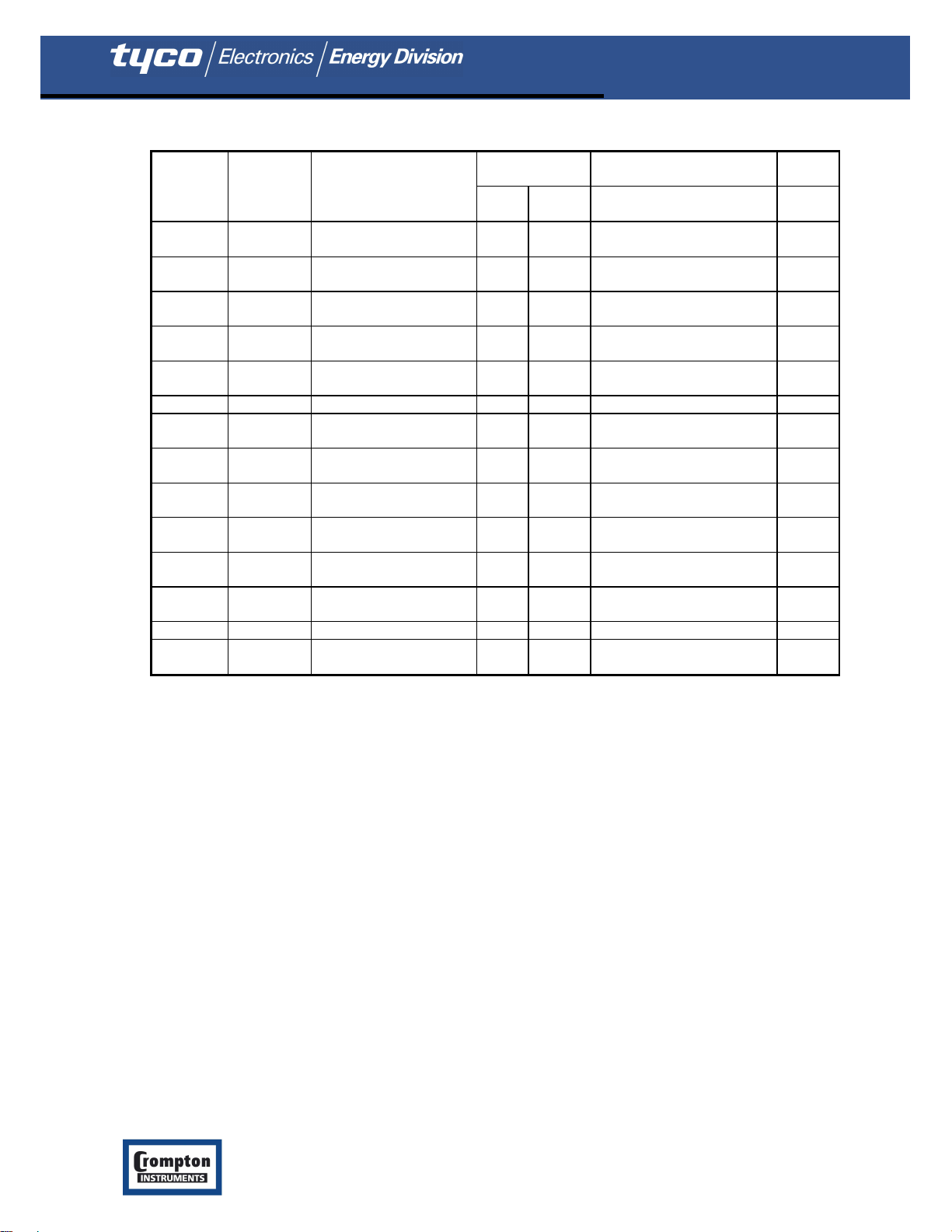
Modbustm Start
Address
(Register)
40345 173
40347 174
40349 175
40351 176
40353 177
40355 178 Analogue 3 Output Top 01 62 Analogue Hardware Max r/wp
40357 179
40361 181
40363 182
40363 182
40361 181
40361 181
40361 181 Analogue 4 Output Top 01 68 Analogue Hardware Max r/wp
40361 181
r/w = read/write r/wp = read and write with password clearance ro = read only wo = write onl y
Some registers marked wo above may in fact be read, but the value returned is not valuable.
It is perfectly feasible to change Integra set-up using a general purpose Modbus
easier to use the Integra disp lay or Integra configurator software. The Integra configurator software has
facilities to store configurations to disk for later retrieval and rapid set up of similarly configur ed products.
Password Settings marked r/wp require the instrument password to have been entered into the
Password register before changes will be accepte d. Once the instrumen t configuration has been
modified, the password should be written to the pa ssword register again to protect the configuration from
unauthorised or accidental cha nge. Power cycling also restores prot ection. Reading the Password
register retur ns 1 if the instrument is unprotected and 0 if it is protected from changes.
* Demand Time
accomplish this. Writing any other value will cause an error to be retu r ned. Reading this register after
instrument restart or resetting demand period gives the number of minutes of demand data up to a
maximum of the demand period setting. For example, with 15 minute demand period, from reset the
value will increment from zero every mi nute until it reaches 15. It will remain at this value until a
subsequent reset occurs.
Demand Period
Writing any other value will caus e an error to be returned.
System Voltage in a PT/VT connected system represents the PT/VT primary voltage. In a direct
connected (i.e. no PT.VT) system this param eter should be set the same as secondary volts.
System Current
Parameter
Number
Analogue 3 Out put
Parameter
Analogue 3 Parameter
Max
Analogue 3 Parameter
Min
Analogue 3 Reading
Top
Analogue 3 Reading
Bottom
Analogue 3 Out put
Bottom
Analogue 4 Out put
Parameter
Analogue 4 Parameter
Max
Analogue 4 Parameter
Min
Analogue 4 Reading
Top
Analogue 4 Reading
Bottom
Analogue 4 Out put
Bottom 01 68 Analogue Hardware Min r/wp
is used to reset the demand period. A va lue of zero must be wr itten to this register to
represents demand time in m inutes. The value written must be one of 8,15, 20 or 30,.
is the CT primary current.
Parameter
Address Hex
High
Byte
01
01
01
01
01
01
01
01
01
01
01
Low
Byte
58
60 ro
62 ro
64 Analogue 3 Parameter Max r/wp
60 Analogue 3 Parameter Min r/wp
64 Analogue Hardware Min r/wp
68
70 ro
70 ro
68 Analogue 4 Parameter Max r/wp
68 Analogue 4 Parameter Min r/wp
Valid range
See table below
(section1.4)
See table below
(section1.4) r/wp
tm
master, but oft en
Mode
r/wp
8 Integra Comms Issue 1 Jan 2006
System Type
single phase 3 wire.
Relay Pulse Width
ms), 5 (100 ms) or 10 (200 ms) are supported. Writing any other value will cause an error to be returned.
Reset Energy is used to reset the Energy readings. A value of zero must be written to this register to
accomplish this. Writing any other value will cause an error to be retur ned.
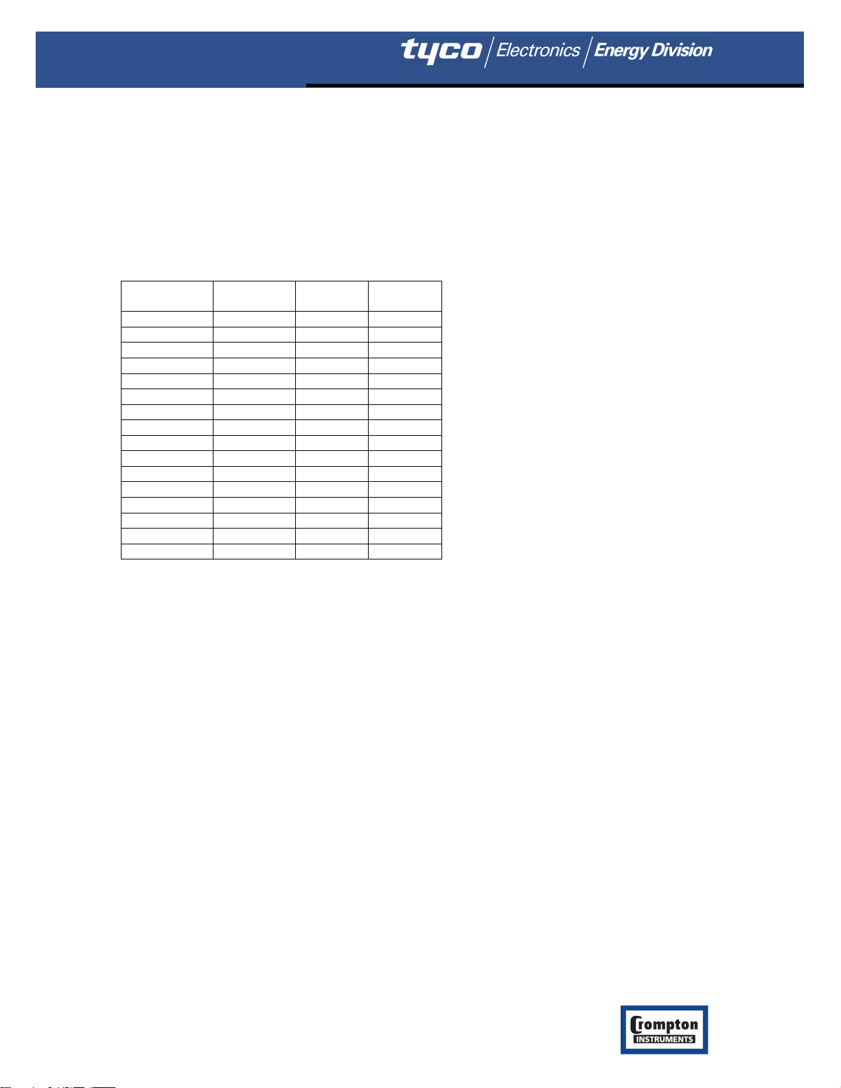
RS485 Set-Up Code
Baud Rate Parity Stop Bits Decimal
19200 NONE 2 30
19200 NONE 1 14
19200 ODD 1 13
19200 EVEN 1 12
9600 NONE 2 26
9600 NONE 1 10
9600 ODD 1 9
9600 EVEN 1 8
4800 NONE 2 22
4800 NONE 1 6
4800 ODD 1 5
4800 EVEN 1 4
2400 NONE 2 18
2400 NONE 1 2
2400 ODD 1 1
2400 EVEN 1 0
Codes not listed in the table above may give rise to unpredi ctable results inc luding loss of
communication. Exercise caution when attempting to change mode via direct Modbus
display or the Integra configurator software is recommended.
Node Address
can be set.
Pulse Rate Divi s or supports only values o f 1,10,100 or 1000. Writing any other value will c ause an error
to be returned.
System Power
system current.
Register Order
or reversed register order. In normal mode, the two registers that make up a floating point number are
sent most signifi cant bytes first. In reversed register mode, the two registers that make up a floating point
number are sent least significant bytes first. To set the mode, write the value '2141.0' into this register the instrument will detect the or der used to send this value and set that order for all Modbus
transactions involving floating point numbers.
Secondary Volts
the value of System Volts . The value of this register c an be set to between the minimum and max i mum
instrument input voltage.
Maximum Energy Count
before they roll over (i.e. resets to zero). The values of 6, 7 or 8 can be written to thi s register to indicate
the number of digits to use. Other values will be rejected.
Analogue Hardware Minimum
is set to '1' fo r single phase 2 wire, '2' for 3 Phase 3 Wire, '3' for 3 Phase 4 Wire or 4 for
is the width of the relay pulse in multip les of 20 ms. However, only values of 3 (60
Value
tm
writes. Use of a
is the Modbus
tm
or JC N2 slave addr ess for the instrument. Any value between 1 and 247
is the maximum system power based on the values of system type, system volts and
controls the order in which the Integra receives or sends floating-point numbers: - normal
tm
indicates the voltage on the VT secondary when the vo ltage on the Primary is equal to
controls the number of digits the energy (kWh and kvarh) counters can use
Analogue Hardware Maximum
and
indicate res pectively the minimum
Integra Comms Issue 1 Jan 2006 9

and maximum outp ut currents that the instrument analogue output hardware is capable of.
Analogue 1 Output Parameter indicates the number o f the input parameter that is to be ou tput on
analogue output 1. A value of zero signifies the analogue output is unused.
Analogue 1 Parameter Maximum
Analogue 1 Parameter Minimum
Analogue 1 Reading Top
can range between Parameter Minimum and Parameter Maximum.
Analogue 1 Reading Bottom
value can range between Parameter Minimum and Parameter Maximum.
Analogue 1 Output Top
reading reaches Reading Top. The value of Output Top must be between Analogue Hardware Minimum
and Analogue Hardware Maximum.
Analogue 1 Output Bottom
parameter reading reaches Reading Bottom. The value of Outpu t Bottom must be between Analogu e
Hardware Minimum and Analogue Hardw are Maximum.
Analogue 2, 3 and 4
to the relevant analogue channel. Analogue 3 and 4 are only relevant for the 1560/1580. Consult the
1560/80 manual for det ails of auto conf ig ure oper at ion , w hich in some cir cumstances overrides user
settings.
Note: Analogue Hardwar e Maximum and M inimum refer to the fact ory build hard ware limits. It is the
same for all analogue channels on a particular instrument.
represents the upper limit of the parameter value that will be output. This value
represents the analogue output level that will be achieved when the parameter
set up values function in the same way as Analogue 1, except of course, they refer
is the maximum value that the selected input parameter c an r each.
is the minimum value that the selected input parameter can r each.
represents the lower limit of the parameter value that will be outp ut. This
represents the analog ue outp ut level th at will be ac hieve d when the
10 Integra Comms Issue 1 Jan 2006
 Loading...