

Page 1

Page 2

CROMEMCO
ZPU
Instruction
Manual
Part
No.
023-0012
CROMEMCO,
280
Mountain
Copyright
Bernardo
View,
INC.
Avenue
CA
1978
94040
September
1978
Page 3
ZPU
INSTRUCTION
MANUAL
Section
Section
Section
1:
2:
2.1
2.2
2.3
2.4
2.5
2.6
3:
TABLE
INTRODUCTION
OF
CONTENTS
•••••••••••••••.••••••••••.••••••••
OPERATING INSTRUCTIONS
POWER-ON
Z-80A
WAIT
ADDRESS
REFRESH ENABLE
ALTAIR
THE
S-100
CLOCK
STATE
MIRROR
OR
JUMP
••••••••••••••••••••••••••••••••••
FREQUENCY
SELECTION
SELECTION
...•.•••...•...•..•.•.......••...
IMSAI INSTALLATION
BUS
•.••••••.•••••••••••••••.•••••••••
.•••••••••••••••••.••••••
SELECTION
••••••••••••••••
••••••.••••••••••••••••••••
•••••••••••••••.••.••••
••.•••••
;
••••.•••••
2
3
3
6
7
9
9
10
11
Section
4:
ASSEMBLY
ZPU
PARTS
INSTRUCTIONS
LIST
•••••••••••••••••••••••.•••••••••
••••••••••••.•••••••••••••
19
23
Page 4
ZPU
INSTRUCTION
MANUAL
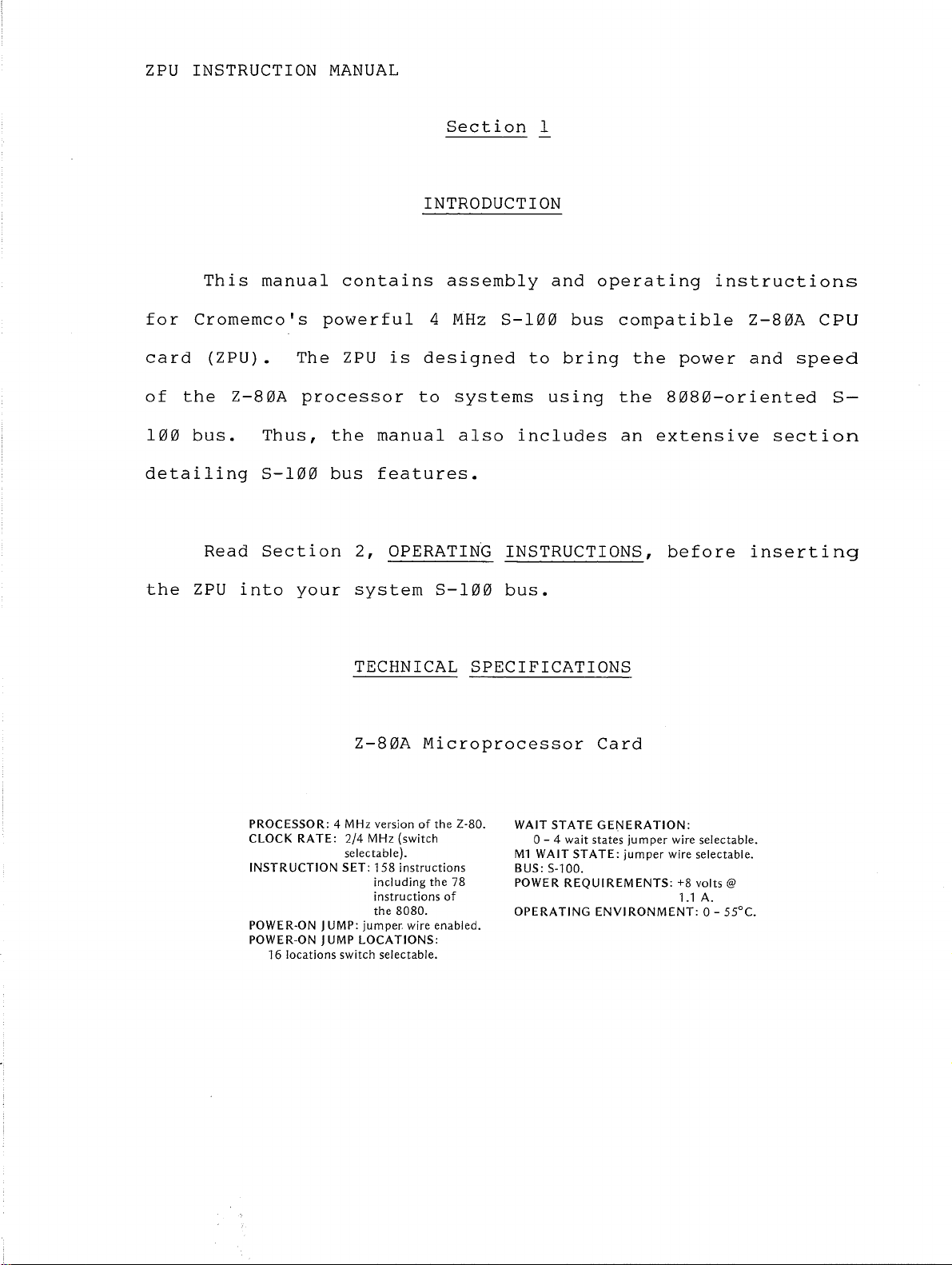
This
for
Cromemco's
card
of
the
100
bus.
detailing
Read
the
ZPU
(ZPU).
Z-80A
into
manual
The
processor
Thus,
S-100
Section
your
contains
powerful
ZPU
the
manual
bus
features.
2,
system
Section
1
INTRODUCTION
is
assembly
4
MHz
designed
to
systems
also
S-100
and
bus
to
bring
using
includes
operating
compatible
the
the
an
OPERATING INSTRUCTIONS,
S-100
bus.
instructions
power
8080-oriented
extensive
before
Z-80A
and
speed
section
inserting
CPU
s-
TECHNICAL
Z-80A
PROCESSOR: 4 MHz version
CLOCK
RATE:
INSTRUCTION
POWER-ON JUMP:
POWER-ON JUMP
16 locations switch selectable.
2/4
MHz
selectable).
SET:
158
including
instructions
the
jumper
LOCATIONS:
(switch
instructions
8080.
SPECIFICATIONS
Microprocessor
of
the
Z-80.
the
78
of
wire
enabled.
WAIT
STATE
o- 4 wait
Ml
WAIT
BUS: S-100.
POWER
OPERATING
STATE:
REQUIREMENTS:
Card
GENERATION:
statesjum
ENVIRONMENT:
per
jumper
wire
wire selectable.
selectable.
+8 volts @
1.1 A.
0 -
55°C.
Page 5
ZPU
INSTRUCTION
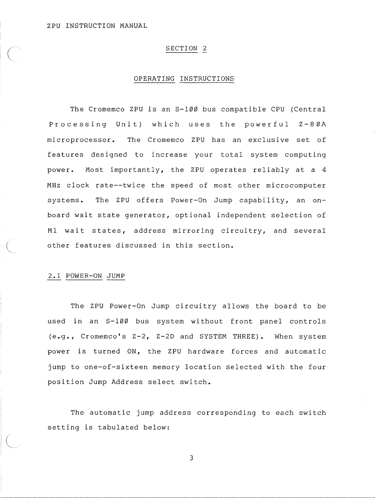
The
Cromemco
MANUAL
SECTION 2
OPERATING INSTRUCTIONS
ZPU
is
an
S-100
bus
compatible
CPU
(Central
Processing
mi c
roprocesso
features
power.
MHz
clock
systems.
board
Ml
wait
wait
other
2.1
POWER-ON
The
designed
Most
states,
features
ZPU
Unit)
r.
importantly,
rate--twice
The
ZPU
state
discussed
JUMP
Power-On
which
The
Cromemco
to
increase
the
offers
generator,
address
Jump
the
speed
Power-On
optional
mirroring
in
this
circuitry
uses
Z
PU
your
ZPU
of
section.
the
has
an
total
operates
most
Jump
independent
circuitry,
allows
powerful
exc1usive
system
reliably
other
capability,
the
Z-80A
set
computing
at
microcomputer
an
selection
and
board
several
to
of
a 4
on-
of
be
used
(e.
g.,
power
jump
position
setting
in
an
Cromemco
is
turned
to
one-of-sixteen
Jump
The
automatic
is
tabulated
S-100
I s
Address
Z-2,
ON,
bus
jump
below:
system
Z-2D
the
memory
select
address
ZPU
wi
thout
and
SYSTEM
hardware
location
switch.
corresponding
3
front
THREE).
forces
selected
panel
and
with
to
controls
When
automatic
the
each
system
four
switch
Page 6
ZPU
INSTRUCTION
MANUAL
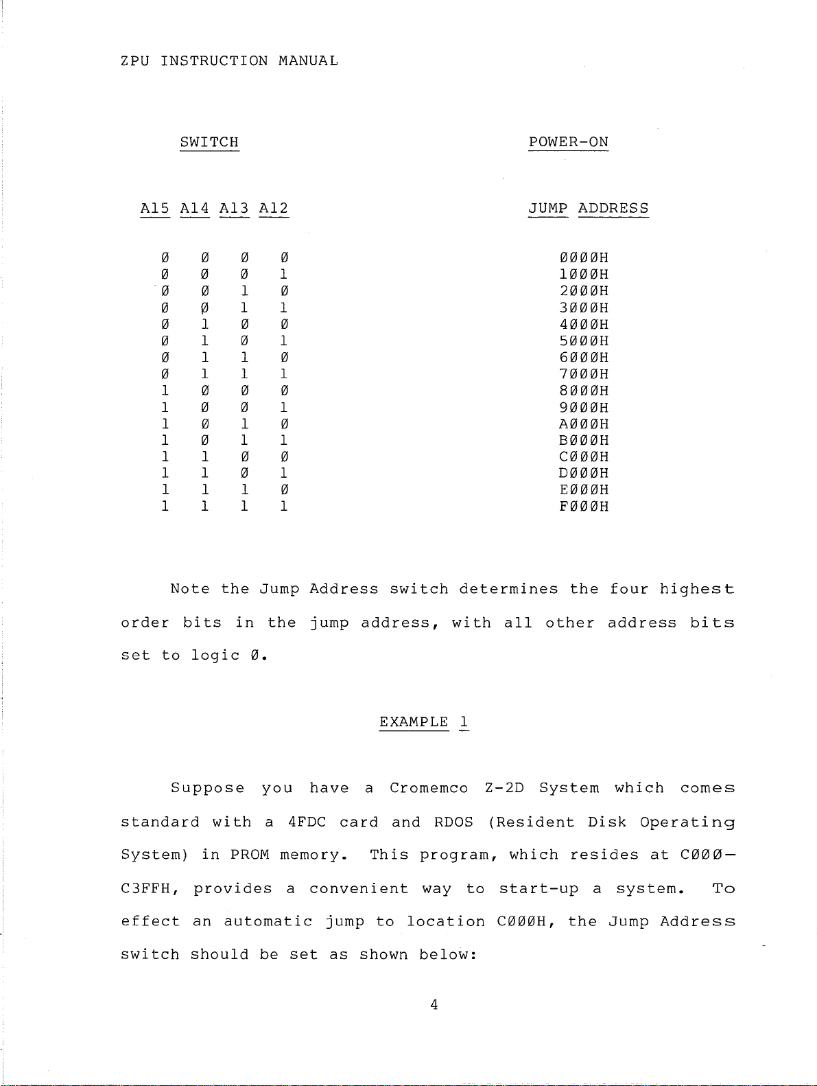
SWITCH
A15 A14 A13 A12
0 0 0 0
0 0 0
0 0
0
0
0
0
0
1
1
1
1
1 1
1
1
1
1 1
0
1 0 0
1 0 1
1 1
1 1 1
0 0 0
0 0
1
0
1 1 B000H
0
0 0
1
0 1 D000H
1 1
1 1 1 1
POWER-ON
JUMP
ADDRESS
0000H
1
0
1000H
2000H
3000H
4000H
5000H
0
6000H
7000H
8000H
1
0
9000H
A000H
C000H
0
E000H
F000H
Note
order
set
to
standard
System)
C3FFH,
effect
switch
bits
logic
Suppose
with
in
provides
an
should
the
Jump
in
the
0.
you
a
PROM
automatic
be
Address
jump
have
4FDC
memory.
a
convenient
jump
set
as
address,
a
card
shown
switch
EXAMPLE
Cromemco
and
This
to
program,
location
below:
with
RDOS
way
determines
all
1
Z-2D
(Resident
which
to
start-up
C000H,
the
other
System
resides
the
four
address
Disk
a
Jump
which
Operating
at
system.
highest
bits
comes
C000-
To
Address
4
Page 7
ZPU
INSTRUCTION
MANUAL
JUMP
ADDRESS
1 0
-zo
c:::::J
.....
CL]N
D:]w
CC~
EXAMPLE 2
14
13
12
15
Suppose
force
Power-On
E3FFH,
as
shown
Your
fea
ture
a
jump
or
so
below:
enabled.
you
ZPU
you
to
RESET.
would
is
have
the
To
a
The
then
factory
disable
Cromemco
Z-81O
Z-81O
set
Monitor
the
JUMP
ADDRESS
1 0
-zo
c:::::J
c::::JN
c:::::J
c::c~
shipped
Moni
Jump
.....
w 13
the
Z-2
tor
15
14
12
function
System,
program
spans
Address
with
and
after
addresses
switch
the
(resulting
you
a
Power-On
want
system
to
to
EIOIOIO-
EIOIOIOH
Jump
in
an
automatic
RESET),
the
board
I f
panel
jump
carefully
labeled
you
controls,
to
address
cut
the
"JUMP
r
com
put
e r s y s t em
the
function
IOIOIOIOH
foil
ENABLE".
trace
has
of
5
only
each
on
a
connecting
RE
SET
of
Power-On
and
these
EXAMINE
two
swi
Clear
points
tches
fro
or
on
n t
is
Page 8
ZPU
INSTRUCTION
MANUAL
altered
Following
not
at
addresses
Immediatley
twice
to
actual
in
clear
examine
For
you
can
switch,
appear
when
a
address
order
the
computers
see
then
in
the
system
specified
after
to
automatic
operation.
how
raising
DATA
the
0000H,
a
examine
the
automatic
RESET,
RESET,
jump
with
Power-On
the
display.
the
but
with
the
the
front
RESET
fi
rather
EXAMINE
automatic
and
panel
Jump
switch.
rst
the
a
This
jump
second
works
feature
instruction
at
one
Jump
switch
jump
time
switches
by
The
is
the
of
Address
must
location:
to
and
pressing
number
op
is
enabled.
executed
the
switch.
be
perform
indicators,
the
C3H
code
sixteen
toggled
once
STOP
should
of
is
the
the
hardware
switch;
the
NEXT
low
switch
will
will
Jump
2.2
Address
Z-80A
The
nsec
cycle
operating
now
all
jump
all
order
appear
be
CLOCK
Z-80A
instruction.
0's
8
bits
again;
0's,
switch
FREQUENCY
may
time)
frequency
will
in
and
or
the
bits.
be
2
appear
of
the
the
MHz
is
the
high
DATA
higher
SELECTION
clocked
(wi
switch
in
jump
order
display.
th
Now
the
address.
8
four
at
ei
a
500
selectable
press
DATA
bits
ther
nesc
bits
display
of
The
4
the
Press
the
lower
will
MHz
cycle
with
EXAMINE NEXT
indicating
the
jump
display
(wi
time).
four
th
the
EXAMINE
address
bits
the
a
250
The
toggle
switch
labeled
"2"
(2
MHz)
and
"4"
6
(4
MHz).
Page 9
ZPU INSTRUCTION
MANUAL
The
used
by
System
labeled
products).
OFF
for
2.3
WAIT STATE
The
match
access
insertion.
the
front
2
the
line
"4
MHz
ZPU
time.
previously
ZPU
panel
MHz"
The
operation.
SELECTION
features
Z-80A
The
as
a 4
(i
t
indicator
clock
The
first
labeled
MHz
indicator
may
be
an
ZPU
inserts
indicator
labeled
will
be
on-board
frequency
allows
from
"STACK"
which
ON
two
on
the
line.
The
monitors
"STACK"
for
4
MHz
WAIT STATE
to
your
system's
types
0
to
3
wait
S-100
Cromemco
this
on
non-Cromemco
operation,
generator
of
wait
state
bus
line
memory
state
cycles
is
Z-l
is
and
to
(1
cycle
every
machine
additional
(referred
the
timing
If
in
its
sta
te
select
Wait
state
accomplished
(just
to
=
250
wait
to
requirements
you
are
factory
i
the
nsec
cycle;
states
as
an
using
wired
on
is
selection
by
re-configuring
left
Ml-cycle
done
of
at
the
second
during
are
Cromemco
condition
the
Z-80A
4 MHz;
an
in
the
on
the
to
accomodate
500
type
instruction
the
tightest.
memory
(no
memo
ZPU
chip).
nsec
inserts
Zilog
boards,
wait
ry
board
at
either
fetch
literature),
states);
boards
other
jumpers
2 MHz)
cycle
leave
if
boards
one
your
all
requi
Ml
during
or
only
where
ZPU
wait
red.
and
no
is
W
7
Page 10

ZPU
INSTRUCTION
A
jumper
MANUAL
wire
M~
~=\W
2.
3.
from
"w"
to
points
labeled
0,
1,
2
and
3
selects
jumper
either
When
requires
Each
requi
state
nsec
operation
nsec
(approx.
to
be
0,
wi
re
0
or
opera
additional
red
slows
per
t i
no
memory
(approx.)
are;
W-wait
)
somewhat
1,
for
2
from
1
ng
wait
the
no
an
or
3
wait
"Ml"
additional
the
required
conservative
states
W-wait
access
•
wait
state
Ml-wait
ZPU
The
states
states
to
points
wait
at
4
to
be
compatible
state
time
memory
corresponding
added,
(from
by
for
state.
in
states
MHz,
250
access
and
actual
on
labeled
500
You
every
a
one
an
during
250
nsec,
time
nsec
may
practice.
machine
0
nsec
with
to
three)
whi
an
figures
memory
additional
find
cycle.
and
the
le
additional
1
an
Ml
memory
Z-80A
slows
an
for
boards,
these
To
selects
Ml-wai
235
figures
get
cycle.
boa
rd
CPU.
the
110
2 MHz
500
nsec
the
A
t
maximum
experimentally
for
reliable
The
a
change
foil
trace
performance
find
operation.
ZPU
comes
is
necessary,
between
from
the
factory
points
fewest
pre-wired
carefully
labeled
your
memory,
number
8
cut
of
for
"w"
the
wait
no
and
you
states
wait
factory
"0",
may
states.
wish
required
installed
or
to
If
between
Page 11

ZPU
INSTRUCTION
MANUAL
"Ml"
and
wires.
2.4
ADDRESS MIRROR
The
address
of
the
inherent
this
behavior
compatibility
The
"0"
8080
of
an
address
in
address
as
microprocessor
I/O
port
bus.
the
Z-80A
through
when
mirror
appropriate
SELECTION
in
both
Although
CPU,
address
updating
circuitry
the
older
before
repeats
the
this
ZPU
mirror
high
board
8080
is
installing
(or
mirrors)
and
characteristic
is
circuitry
systems.
enabled
low
designed
by
the
new
the
order
to
assuring
short
jumper
8-bi
8
bits
is
mimic
t
not
ZPU
run
of
foil
IC8
on
carefully
connect
2.5
REFRESH ENABLE
ref
resh
eight
install
ENAB".
broken
between
the
pads
Certain
add
high
a
as
cut
The
board).
"AM"
types
ress
order
jumper
ZPU
no
pads
the
existing
and
of
supplied
address
wire
is
Cromemco
labeled
If
you
"OFF"
dynamic
between
factory
wish
foil
with
by
lines.
memory
"AM"
a
memory
the
the
shipped
and
to
trace,
jumper
Z-80A
To
boards
"ON"
disable
boards
enable
two
with
and
wire.
be
pads
(between
this
in
require
mirro
this
labeled
this
require
IC7
circuitry,
its
place,
that
red
in
feature,
connection
address
and
the
the
"RFSH
mirroring.
9
Page 12

ZPU
INSTRUCTION
2.6
ALTAIR
If
the
front
ZPU
board.
If
you
you
MANUAL
OR
IMSAI INSTALLATION
are
panel
are
using
may
using
an
be
an
IMSAI
plugged
ALTAIR
8080
directly
8800
computer,
into
or
8800A
the
socket
computer,
cable
Jl
on
from
a
the
DIP
plug
front
data
connector
figure
must
be
panel
lines
below
cord.
as
ZPU
installed
are
for
not
they
wiring
SOCKET
When
are
in
place
wiring
arranged
on
information).
Jl
IIIIIIII
D7
D6
D5 D4
D3
D2
Dl
D0
the
of
the
the
connector,
sequentially
ZPU
connector
ALTAIR
o 0 0 0 0 0 0 0
D3
Molex
D2
connector
on
MOLEX
Dl
D0
note
the
(refer
CONNECTOR
D4
that
D5
on
the
the
ALTAIR
to
the
D6
D7
10
Page 13

ZPU
INSTRUCTION
MANUAL
The
Cromemco
microprocessor
bus,
many
in
turn,
as
processor
the
IIAltair
computers
microcomputer
Dr.
Roger
20
additional
modules.
ll
in
1975.
manufacturers
Melen
to
is
bus
ZPU
the
designed
of
Cromemco
THE
card
industry
This
bus
appearing
The
bus
Section
S-100
is
designed
to
memory,
standard
was
and
Inc.
3
BUS
standard
interface
I/O
in
the
quickly
was
in
to
S-100
interface,
was
MITS
named
August
interface
a
CPU
originally
adopted
the
of
the
bus.
The
module
or
known
Altair
by
line
a
IIS-10011bus
1976.
to
host
The
Z-80A
S-100
as
other
as
of
of
by
S-
100,
or
most-used
industry.
Physically,
contact
wired
connectors
10
11
•
by
The
module
IIStandard-100
busing
edge
in
connectors
parallel.
of
the
S-100
using
the
bus
standard
the
S-100
was
8080
11
,
bus
is
ever
S-100
bus
mounted
The
bus
modules
are
originally
microprocessor,
now
developed
is
realized
to
circuit
designed
widely
a common
that
plug
cards
and
regarded
in
as
a
mother
into
that
for
use
consequen
the
set
as
computer
of
board
the
measure
with
tl
y,
100-
edge
a
the
and
5
CPU
the
11
bus
system.
signal
The
definitions
Z-80A
closely
microprocessor
11
follow
signal
those
lines
of
differ
an
8080
qui
te
Page 14

ZPU
INSTRUCTION
MANUAL
dramatically
by
a
single
the
ZPU
functions
the
1)
control
is
S-100
power
shown
I.
2.
3.
4.
5.
6.
7.
8.
9.
10.
II.
12.
13.
14.
15.
16.
17.
18.
19.
20.
2I.
22.
23.
24.
25.
+8
+18
EXT.
UNDEFINED
NMI
UNDEFINED
STATUS
CONTROL
UNPROT.
SINGLE
ADDR.
DO
¢2
1>1
from
phase
board
(including
bus
supply,
signals.
below:
VOLTS
VOLTS
READY
"
"
"
"
"
"
"
"
"
"
"
DISAB.
DISAB.
MEM.
STEP
DISAB.
DISABLE
CLOCK
CLOCK
is
can
the
clock,
designed
the
be
grouped
2)
A
complete
26.
27.
28.
29.
30.
3I.
32.
33.
34.
35.
36.
37.
38.
39.
40.
4I.
42.
43.
44.
45.
46.
47.
48.
49.
50.
8080
the
to
two
address,
S-100
pHLDA
pWAIT
pINTE
A5
A4
A3
A15
A12
A9
DOl
D00
A10
D04
D05
D06
DI2
DI3
DI7
sMl
sOUT
sINP
sMEMR
sHLTA
2
MHz
GROUND
lines
8080
supply
phase
in
listing
CLK.
four
3)
BUS
(e.g.,
by
all
clock).
data,
of
5I.
52.
53.
54.
55.
56.
57.
58.
59.
60.
6I.
62.
63.
64.
65.
66.
67.
68.
69.
70.
7I.
72.
73.
74.
75.
the
a
two
"8080-like"
functional
the
+8
-18
SSW
EXT.
UNDEFINED
MEM.
REFRESH
UNDEFINED
MEM.
PROTECT
PROTECT
RUN
pREADY
pINT
pHOLD
pRESET
Z-80A
phase
The
and
S-100
VOLTS
VOLTS
DISABLE
CLEAR
"
"
REQUEST
WRITE
is
clock),
S-100
signals
categories:
4)
clock
bus
STAT.
MEM.
driven
signals
76.
77.
78.
79.
80.
8I.
82.
83.
84.
85.
86.
87.
88.
89.
90.
9I.
92.
93.
94.
95.
96.
97.
98.
99.
100.
but
bus
of
and
pSYNC
pWR
pDBIN
A0
Al
A2
A6
A7
A8
A13
A14
All
D02
D03
D07
DI4
DI5
DI6
DII
DI0
sINTA
sWO
sSTACK/4
PWR-ON
GROUND
MHz
CLEAR
12
Page 15

ZPU
INSTRUCTION
MANUAL
S-100
the
powe
must
three-terminal
POWER
Three
S-100
r
supplies
be
performed
Distributed
SUPPLY
unregulated
bus:
are
regulator
+8
volts,
on
power
+8
Volts
+18
Volts
-18
Volts
Ground
D.C.
unregula
each
IC's.
power
+18
volts
ted,
individual
supply
supply
and
so
power
circuit
regulation
Pins
Pin
Pin
Pins
-18
1
and
2
52
50
and
voltages
volts.
supply
card,
51
has
100
appear
The
regula
usually
several
on
main
t i
on
by
advantages
-Each
Faul
entire
-The
distributed
-Voltage
the
-Initial
card
ty
heat
card
over
is
regulation
computer
produced
through
drops
circuitry
cost
a
indi
system.
along
of
single,
vidually
in
itself.
the
one
by
a
larger
the
computer
centrally
protected
master
voltage
physical
bus
do
mainframe
regulated
supply
regulation
not
from
cannot
volume.
influence
is
supply:
vol
lower.
tage
is
the
overload.
destroy
thermally
voltage
Regulation
the
on
circuitry
is
purchased
only
as
13
additional
cards
are
added
to
Page 16

ZPU
INSTRUCTION
the
system.
An
S-100
MANUAL
bus
mainframe
capable
of
accepting
a
full
21
cards
typically
+8
volts
S-100
There
(like
has
and
ADDRESS
are
the
a
power
15
amps
SIGNALS
16
Cromemco
supply
at
A0
Al
A2
A3
A4
AS
A6
A7
address
+18
PIN
PIN
PIN
PIN
PIN
PIN
PIN
PIN
and
79
80
81
31
30
29
82
83
lines
Z-2,
current
-18
on
Z-2D
volts.
A8
A9
A10
All
A12
A13
A14
A15
the
and
capacity
PIN
PIN
PIN
PIN
PIN
PIN
PIN
PIN
S-100
SYSTEM THREE)
of
30
amps
84
34
37
87
33
85
86
32
bus
allowing
at
the
direct
TTL
drivers
cont
address
to
take
addressing
rol
1i
ne
drivers
control
are
(ADDRESS
used
to
of
of
allow
the
65,536
to
drive
DI
address
words
SABLE)
DMA
of
the
address
can
operations
bus.
14
memory
be
used
when
bus.
space.
to
other
One
disable
Tri-state
S-100
cards
bus
the
need
Page 17

ZPU
INSTRUCTION
MANUAL
S-100
mi c
roprocesso
the
The
DATA
Although
S-100
data
SIGNALS
r
has
input
the
which
two
bus
DI0
DIl
DI2
DI3
DI4
DI5
DI6
DI7
directional
is
PIN
PIN
PIN
PIN
PIN
PIN
PIN
PIN
S-100
has
called
95
94
41
42
91 D04
92
93
43
bus
an
8-bi
data
the
D00
DOl
D02
D03
D05
D06
D07
t
DI
is
bi-di
busses,
bus,
PIN
36
PIN
35
PIN
88
PIN
89
PIN
38
PIN
39
PIN
40
PIN
90
based
rectional
each
and
the
on
8
the
da
bits
data
ta
output
8080
bus,
wide.
bus
line
S-100
is
to
CLOCK
called
disable
EXT
NMI
STATUS
CONTROL
UNPROTECT
SINGLE STEP
ADDR.
DO
cjJ2
¢l
pHLDA
pWAIT
pINTE
sMl
sOUT
sINP
sMEMR
the
AND
READY
DISABLE
DO
the
CONTROL
DISAB.
DISAB.
DISAB.
bus.
DO
The
bus
SIGNALS
PIN
PIN
PIN
PIN
PIN
PIN
PIN
PIN
PIN
PIN
PIN
PIN
PIN
PIN
PIN
PIN
PIN
(DO
3
12
18
19
20
21 PROTECT STATUS
22
23
.24
25
26
27
28
44
45
46
47
S-100
DISABLE)
SSW
EXT.
MEM.
REFRESH
MEM.
PROTECT
RUN
pREADY
pINT
pHOLD
pRESET
pSYNC
pWR
pDBIN
sINTA
sWO
provides
for
DISABLE
CLEAR
REQ.
WRITE
for
DMA
one
control
operations.
PIN
53
PIN
54
PIN
65
PIN
66
PIN
68
PIN
69
PIN
70
PIN
71
PIN
72
PIN
73
PIN
74
PIN
75
PIN
76
PIN
77
PIN
78
. PIN
PIN
96
97
15
Page 18

ZPU
INSTRUCTION
MANUAL
There
25),
1 i
clock
overlappi
clock
levels.
equivalent
ne
¢2_(pin
is
Control
sHLTA
2
MHz
are
always
frequency.
ng
and
control
CLOCK
three
24)
c
locks
signals
to
and
a 2
clock
2
MHz
¢l
at
signals
on
control
PIN
PIN
MHz
signal
and
the
the
48
49
signals
Clock
¢2
processo
on
the
S-100
signals
sSTACK/4
PWR-ON CLEAR
on
the
(pin
rega
provide
S-100
bus
rdless
r
49).
clock
bus
which
used
Mhz
S-100
of
a
are
bus:
The
two
frequency.
are
with
2
the
phase
standard
functionally
PIN
PIN
¢l
MHz
processo
the
98
99
(pin
CLOCK
r
non-
All
TTL
8080
microprocessor
pHLDA,
and
control
100
equivalent
latch.
sINTA,
indicate
Cromemco
4
MHz
pWAIT,
pDBIN
signals
bus
These
sWO
Z-80A
operation
Four
serve
signals
to
and
stack
of
are
pINTE,
for
the
signals
sSTACK.
systems,
(logic
the
prefixed
pREADY, pHOLD,
the
prefixed
corresponding
operations
S-100
the
include
1)
same
8080
The
this
or
control
with
function
microprocessor.
with
sMl,
sSTACK
in
line
2
MHz
an
outputs
sOUT,
8080
is
operation
lines
a
pINT,
line
used
lower
as
"s"
of
sINP,
(pin
systems;
instead
are
case
pRESET,
the
Similarly,
are
the
98)
(logic
dedicated
"p".
pSYNC,
corresponding
functionally
8080
sMEMR,
is
however
to
status
sHLTA,
used
indicate
0).
to
Thus
pWR
S-
to
in
tri-
s
tat
i ng
bus
d r iver s (e • g
.,
d
uri
ng D
MA0per
a t
ion
s)
•16ADDRESS
Page 19

ZPU
INSTRUCTION
MANUAL
DISABLE
used
to
to
disable
CONTROL
signals.
Three
wi
th
the
MEMORY
on
the
the
Z-80A
The
is
used
disable
the
DISABLE
of
the
Z-80A
REQUEST,
S-100
bus
microprocessor.
remaining
to
the
status
is
CPU.
and
are
disable
Data
lines
used
S-100
These
REFRESH.
the
ten
defined
Output
(those
to
control
are
same
the
disable
NMI
The
as
lines
add
ress
bus;
STATUS DISABLE
prefixed
the
signals
(Non-Maskable
functions
the
corresponding
are
bus;
with
clock
shown
used
DO
an
are
of
these
primarily
DISABLE
is
"s");
and
control
used
Interrupt),
signals
lines
used
only
in
is
and
of
S100
swi
accidental
70)
UNPROTECT
UNPROTECTED
systems
tch
signal
wi
can
memory
to
(pin
status
PROTECT STATUS
indicate
with
to
pREADY
circuitry
READY
front
line.
a
memory
panel
and
to
be
th
the
(pi
avoid
other
an
operator's
used
write
bus.
20)
of
n
69)
write
memory
circuitry
to
operations
The
signal,
any
signa
operation
deposit.
bus
protect
memory
memory
1.
conflicts
front
and
need
RAM
by
can
the
can
be
MWRITE
and
EXT.
when
control
panel.
or.
issuing
be
unprotected
current
determined
(pi
is
used
READY
A
PROM
a PROTECT
PROTECTED
n
68)
in
is
an
both
of
the
front
panel
memory
by
from
is
used
conjunction
alternate
front
panel
processor
from
(pin
the
or
the
to
Front
panel
controls
can
17
be
used
to
run
or
stop
the
Page 20

ZPU
INSTRUCTION
MANUAL
processor
the
When
input
used
EXTERNAL
panel
Finally,
logic
to
tha
stabilized.
RUN
front
port,
to
0
logic
t
or
(pin
disable
CLEAR
switch,
there
when
1
po
we
to
single
71)
panel
the
power
approximately
r
is
line
sense
SENSE SWITCH DISABLE
the
(pin
but
is
it
the
on
step
DI
54)
is
POWER-ON
is
first
and
and
swi
is
assigned
100
the
through
the
tches
bus
activated
CLEAR
turned
milliseconds
power
a
prDgram
SINGLE STEP
are
during
assigned
(SSW
to
signal
on,
supply
sense
by
no
and
as
(pin
to
DISABLE,
switch
an
auxillary
specific
that
then
later
vol
indicated
21)
a
specific
pin
inputs.
function.
remains
transitions
to
indicate
tages
line.
53)
front
on
is
at
have
18
Page 21

ZPU INSTRUCTION
MANUAL
If
you
straight-forward
All
from
use
(with
less)
parts
the
the
Be
acid
soldering
opposite
sure
core
purchased
are
white
to
solder),
provided
inserted
printed
side.
use
iron.
Section
4
ASSEMBLY INSTRUCTIONS
a ZPU
a
high
and
you
from
legend),
a
kit,
follow
the
quality
fine
you
will
the
component
and
rosin
tipped
all
find
instructions
side
soldering
core
low
wattage
assembly
of
the
solder
below.
is
(DO
(25
to
board
done
NOT
W
be
or
The
position
instruction
( )
Solder
printed
and
step
in
Rl
R2
R3
R4
R5
R6
R7
R8
R9
R10
Rll
R12
R13
legend
orientation
when
position
lK
lK
180
180
270
270
10K
390
330
330
lK
100
180
on
the
of
completed.
the
1/4-watt
(brown-black-red)
(brown-black-red)
(brown-grey-brown)
(brown-grey-brown)
(red-violet-brown)
(red-violet-brown)
(brown-black-orange)
(orange-white-brown)
(orange-orange-brown)
(orange-orange-brown)
(brown-black-red)
(brown-black-brown)
(brown-grey-brown)
component
each
side
component.
5%
carbon
shows
Check
film
the
exact
off
resistors:
each
19
Page 22

ZPU
INSTRUCTION
MANUAL
Jl.
10
THE
Install
Install
mfd
TANTALUM
CAPACITOR
Ins
tall
R14
R15
R16
R17
forty-four
the
IS
SIP
100
330
330
560
IC
twenty-six
CAPACITORS
ALIGNED
res
i s
tor
(brown-black-brown)
(orange-orange-brown)
(orange-orange-brown)
(green-blue-brown)
sockets
for
IC3-IC43,
capacitors.
MAKE
WITH
net
CERTAIN
THE
w0 r ks
"+" PRINTED
RN
3 ,
WHEN
THAT
RN4and
RN1,
RN2
INSTALLING
THE
ON
"+"
THE
RN
5 •
and
THE
END
BOARD.
The
OF
arrow
arrows
ing
IC2)
the
sink.
of
the
tips
with
Install
the
top
Ins
ta
in
the
regulator
Install
heatsink.
printed
numerals
Ql,
of
11
the
the
upper
legs
the
on
the
"1"
a
2N3904
board.
heatsi
nk
left-hand
do
not
speed-select
circuit
printed
transistor,
and
corner
make
toggle
board
on
vo1tage
contact
the
with
regula
of
switch
point
RN
the
with
to
packages.
the
flat
to
r
board.
the
metallic
just
pin
ICs
to
1;
align
side
(ICIand
Make
the
right
fac-
sure
heat
Solder
in
position
the
8.000
20
MHz
crystal
just
to
the
Page 23

ZPU
INSTRUCTION
MANUAL
right
crystal
hole
the
then
right
indicating
(see
board
on
top
solder
Install
Install
of
side
Note
point
by
one
of
the
soldering
side
the
it
the
of
the
all
below).
to
speed-select
of
the
crystal
in
place.
four
the
ON
pin
board.
position
ICs
The
1
(see
a
short
through
posi
and
switch.
crystal,
tion
The
should
resistor
arrow
figure
piece
the
tips
pull
hole
Jump
arrow
point
networks
below).
Mechanically
of
number
the
on
the
Address
on
the
to
printed
wire
the
24
swi
in
on
secure
wire
tightly
opposite
swi
tch
tch
right.
their
the
the
to
the
over
side,
on
the
package
sockets
circuit
After
all
exception
oriented
inserting
of
ICS
PIN 1 -
in
the
(pin
........
~-~-----.;:~-
the
1
same
to
ICs
-
the
..
-r--.==~
and
direction
RNs,
LEFT).
r-_--
verify
(pin
that
1 UP)
they
with
are
the
21
Page 24

ZPU
INSTRUCTION
MANUAL
The
legs.
to
closely
its
socket
inspect
device.
This
board.
particular
bridges
most
To
avoid
match
the
completes
Carefully
between
wi
care
common
this
the
th
legs
inspect
to
pads
assembly
annoying
IC
a
gentle
after
the
see
and
IMPORTANT
faults
problem,
socket
end-to-end
insertion
construction
your
that
there
adjacent
NOTE
span.
work
foil
are
by
of
before
are
bent-under
first
Then
looking
the
no
areas.
bend
"rock"
pressure.
Cromemco
proceeding.
inadvertent
IC
the
the
Visually
beneath
Z-80
and
IC
IC
solder
RN
legs
into
the
CPU
Take
22
Page 25

ZPU
INSTRUCTION
MANUAL
ZPU
PARTS
LIST
(REV E)
Capacitors
Cl
C2
C3
C4
C5
C6
C7
C8
C9
C10
Cll-C24
C25
C26
Integrated
ICl
IC2
IC3
IC4
IC5
IC6
IC7
IC8
IC9
lC10
ICll
IC12
IC13
IC14
IC15
IC16
IC17
IC18
IC19
IC20
IC21
IC22
IC23
IC24
IC25
IC26
IC27
IC28
IC29
IC30
IC31-
LM340T-5
LM340T-5
10
.001
.005
.005
0.1
10
150
56
10
10
0.1
150
10
Circuits
74164
74157
Z-80A
74LS04
74LS10
7400
7474
7404
74367
74367
74367
74367
74LS04
74157
74LS10
7400
7474
74LS04
7474
7408
74367
74367
74367
74367
74367
74S133
74164
7474
74LS04
uF
uF
uF
uF
uF
uF
pF
pF
uF
uF
uF
pF
uF
Part
004-0032
004-0022
004-0025
004-0025
004-0030
004-0032
004-0011
004-0006
004-0032
004-0032
004-0030
004-0011
004-0032
012-0001
012-0001
010-0007
010-0009
011-0010
010-0066
010-0063
010-0000
010-0019
010-0030
010-0080
010-0080
010-0080
010-0080
010-0066
010-0009
010-0063
010-0000
010-0019
010-0066
010-0019
010-0027
010-0080
010-0080
010-0080
010-0080
010-0080
010-0089
010-0007
010-0019
010-0066
No.
IC32
IC33
IC34
IC35
IC36-41
IC42
IC43
Resistors
Rl
R2
R3
R4
R5
R6
R7
R8
R9
R10
Rll
R12
R13
R15
R15
R16
R17
R18
R19
Resistor
RNl
RN2
RN3
RN4
RN5
74LS04
74LS00
74LS02
74367
74LS04
Networks
4.7K
lK
lK
lK
330
7400
7408
180
180
270
270
10K
390
330
330
100
180
330
330
330
180
180
DIP
DIP
SIP
SIP
SIP
lK
lK
lK
lK
010-0000
010-0066
010-0069
010-0068
010-0:080
010-0027
010-0066
Part
001-0018
001-0018
001-0009
001-0009
001-0011
001-0011
001-0030
001-0013
001-0012
001-0012
001-0018
001-0007
001-0009
001-0012
001-0012
001-0012
001-0009
001-0018
001-0009
003-0017
003-0016
003-0007
003-0007
003-0004
No.
23
Page 26

ZPU
INSTRUCTION
Miscellaneous
Ql
2N3404
Xl
8-MHZ
SWI
SPDT
SW2
DIP
SWITCH
HEATSINK
6-32
6-32
#18
SOCKET
22-S0CKETS,
21-S0CKETS,
ZPU
Software
SCREWS
NUTS
WIRE
PC
BOARD
40
14
16
XTAL
SWITCH
(4)
(4)
PIN
PIN
PIN
MANUAL
009-0001
026-0001
013-0000
013-0001
021-0017
015-0000
015-0013
019-0012
017-0006
017-0001
017-0002
CROMEMCO
(PAPER TAPE)
Documentation
Z-80
ZPU
INSTRUCTION
Z-80A
Z-80
MONITOR
CPU
MONITOR
MANUAL
MANUAL
TECHNICAL
MANUAL
24
(
Page 27

ZPU
INSTRUCTION
MANUAL
WARRANTY
Your
materials
date
prove
they
expressed
damages.
period,
Cromemco,
refuse
subject
of
to
are
Should
factory-built
and
delivery.
be
returned
or
it
will
for
to
repa
to
workmanship
defective
implied.
your
abnormal
factory-built
be
a
fixed
i r
any
We
will
during
to
We
repaired
service
product
electrical
ZPU
is
for
repair
Cromemco.
are
provided
warranted
a
period
the
not
ZPU
fee.
tha
tin
or
or
replace
warranty
No
liable
fail
that
We
reserve
our
mechanical
against
of
other
after
90
for
it
opi
defects
days
products
period
warranty
consequential
the
is
returned
the
ni
on
abuse.
from
that
provided
warranty
right
has
been
in
the
is
to
to
The
service
it
is
reserve
opinion
been
Payment
Your
returned
subject
fee
assembled
the
has
of
is
right
not
the
currently
to
Cromemco,
to
been
to
abnormal
service
$70.00
ZPU
kit
refuse
assembled
will
for
repair
electrical
fee
25
and
in
must
is
subject
be
repaired,
a
fixed
of
a
workmanlike
accompany
any
or
to
change.
provided
service
kit
mechanical
that
manner
the
fee.
in
or
abuse.
returned
that
We
our
has
Page 28

ZPU
INSTRUCTION
MANUAL
merchandise.
to
change.
The
service
fee
is
currently
$70
and
is
sUbject
(
26
Page 29

 Loading...