

Page 1
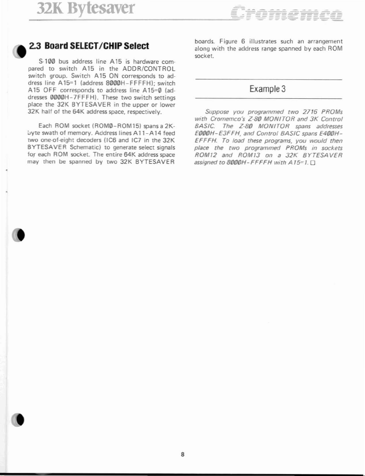
Cromemeo
Five
Dollars
By
31K
te
saver
Page 2
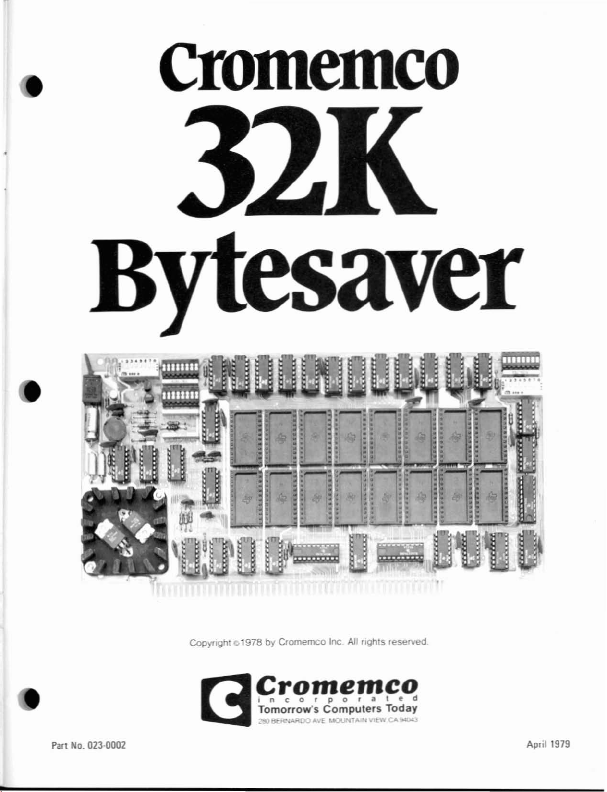
Cromemco
Part
No.
023·0002
CopyrIght c,1978byCromemco
cromemco
irocorpo,.t~d
[3
Tomorrow's
::l!OBER!;AAOO
"'.'E
......
• • •
..
•
; .
..
..
..
Inc A1ll1ghlS reserved
Computers
UOUN1'A N
V'E;W
.
Today
c.\
\joIljolJ
•
April
1979
.
Page 3
Table
Section 1
I
ntraduction.._. _
Technical Specifications
..._.....
of
COntents
_
.........•......•......•..
...........•................
1
,
Section
Operating Instructions.._
2
..._.....
2.1 Switch Options-An Overview
PROGRAM
ADDR/CONTROL Switches
PROGRAM
BANKSE
SHADOW ROM Switches
2.2
Addressing
2.3 Board Select/Chip Select _ _ 8
2.4 Shadowing ROM Socket Pairs _
2.5
Memory
2.6 Select
2.7
Direct Memory Access. _ 16
POWER Toggle
ENABLE
LEer
Banks 12
BANK0On
The
Switches
32K
BYTESAVER.._. _
RESET Or
_
..........•...••......
Switch
Switches
.............••....
•.••••......
POWER·ONCLEAR
_.2
10
16
Section 3
PROM Programming Instructions 19
3.1 Programming From RODS Or
3.2
Programming From 3K Control BASIC
3.3
Programming From
Section 4
Theory Of Operation
4.1 Power Supplies
4.2 Addressing. .
4.3 Memory Read Cycles
4.4 Memory Write Cycles
4.5
DMA
...........••.•...•••......•......
................•..............
................•..............
Cycles
l-80
....................•......
.......•..................
.......•....................
2·80
Monitor 19
Assembly Code
20
22
24
24
24
25
25
25
2
7
Section 5
Assembly Instructions
5.1 Assembly Steps
5.2 Power
Parts List..._. _. _ _
Parts Location Diagram.._. _
Switch Options-Ouick Reference
Warranty _. _ _
Schematic Diagram
line
............•••....•••...........
.........................•.....
Testing
.....••......•...
........•...................
.......•.....••.•..........
.......•.....••......•.....
.........•......•...........
....•......••.....•.....
_. _. _
......•...
27
27
28
30
32
33
34
_..35
Page 4
LIST
OF
ILLUSTRATIONS
TableofCOntents
Figure 1 -
Figure 2 -
Figure 3 - Example 1
Figure 4 - Example 2
Figure 5 •
Figure 6 .
Figure 7 - Example 4
Figure 8 . The
Figure 9 - Example 5
Figure
Figure
Figure
Figure13- IC Pin Position
Switch
ADDR!CONTROL
Locations.
Switch
Switch
32K
BYTESAVER
Two
32K
BYTESAVEAS
Address
Space
Switch
Memory
Switch
10
- Example 5 Memory Map 14
1'-
DMA
OVERRIDE
12-Control
BASIC
.............•....•.........
Switches
Settings
.........•..........
_ _ _ 5
Settings _. _. _. _ _
Addressing..__.__
Spanning
The
64K
_ 9
Settings And Memory Map
Map
With
Multiple
Memory
Banks
Settings 13
Example
Memory
Configuration
Map _
2
3
.6
7
11
12
17
21
28
Page 5

Page 6
32K
Bytesaver
Introduction
This manual provides assembly instructions,
operating
the Cromemco
The
patible.
memory
SAVER features:
• Independent
•
• BANKSELEeT
• ROM
instructions
32K
32K
BYTESAVER
32K-byte
board and programmer.
memory
board.
Independent
grammer.
and
BYTESAVER
capacity.
operation
operationasa
allowing memory expansion
beyond
ory
64K-bytes_
SHADOWING
to
overlap
portions
theory
of
operation
memory
is
an 5-100 bus com-
2716-type
The
32K
asa32K-byte
2716
PROM pro-
allowing
external mem-
of
the
32K
SAVER's address space.
•
Powerful
DMA
DMA
OVERRIDE.
configuration
options
board.
EPROM
BYTE·
ROM
BYTE-
with
for
• Fully
•
Digital
buffered
count
(no erratic one-shots).
• A separate memory
ROM socket.
•
All
options
jumper
This
Operating
tions,
tions.Ifyou
Assembly
struction
"Switch
Instructions
tional overview
quicklytouse.
Theory
wires).
manual consists
Instructions.
of
purchased a
Instructions
and
initial
Options-An
provides a
for
address lines.
derived
SWitch selectable
PROM Programming Instruc-
Operation
test procedures.
Overview"
those
PROGRAM
protect
of
and
32K
BYTESAVEA
provide
32K
BYTESAVER
who
wanttoput
switch
lno
four
basic sections:
Assembly Instruc-
step-by-step con-
of
the
PULSES
for
soldered
kit,
The
section
Operating
the
each
the
opera·
board
Technical Specifications-32K
MEMORY
MEMORY
MEMORY
WAIT
WAIT
BUS
POWER REQUIREMENTS:
OPERATING
CAPACITY:
TYPE:
ACCESS
STATES@2
STATES@4
COMPATIBILITY:
ENVIRONMENT:
·NOTE:
I
32K
BYTES
INTEL
TIME:
MHZ:
MHZ:
450 NANOSECONDS
NONE REQUIRED
ONE
PER
S·100
+B
VOLTS
0-55
DEGREES CELSIUS
Texas Instrument's
equivalenr to the Intel
thus
it
may
not
be
BYTESAVER.
to the Intel
the
32K
BYTESAVER.
The
2716,
soitmaybeused with
BYTESAVER
2716, TI 2516 DR
MACHINE
AT
2.1
2716
PROM
2716
used with the
TI
2516
CYCLE
AMPS
is
PROM. and
IS
equivalenr
PROM
EQUIVALENT'
(MAX.)
Card
not
32K
1
Page 7
Page 8
32K
Bytesaver
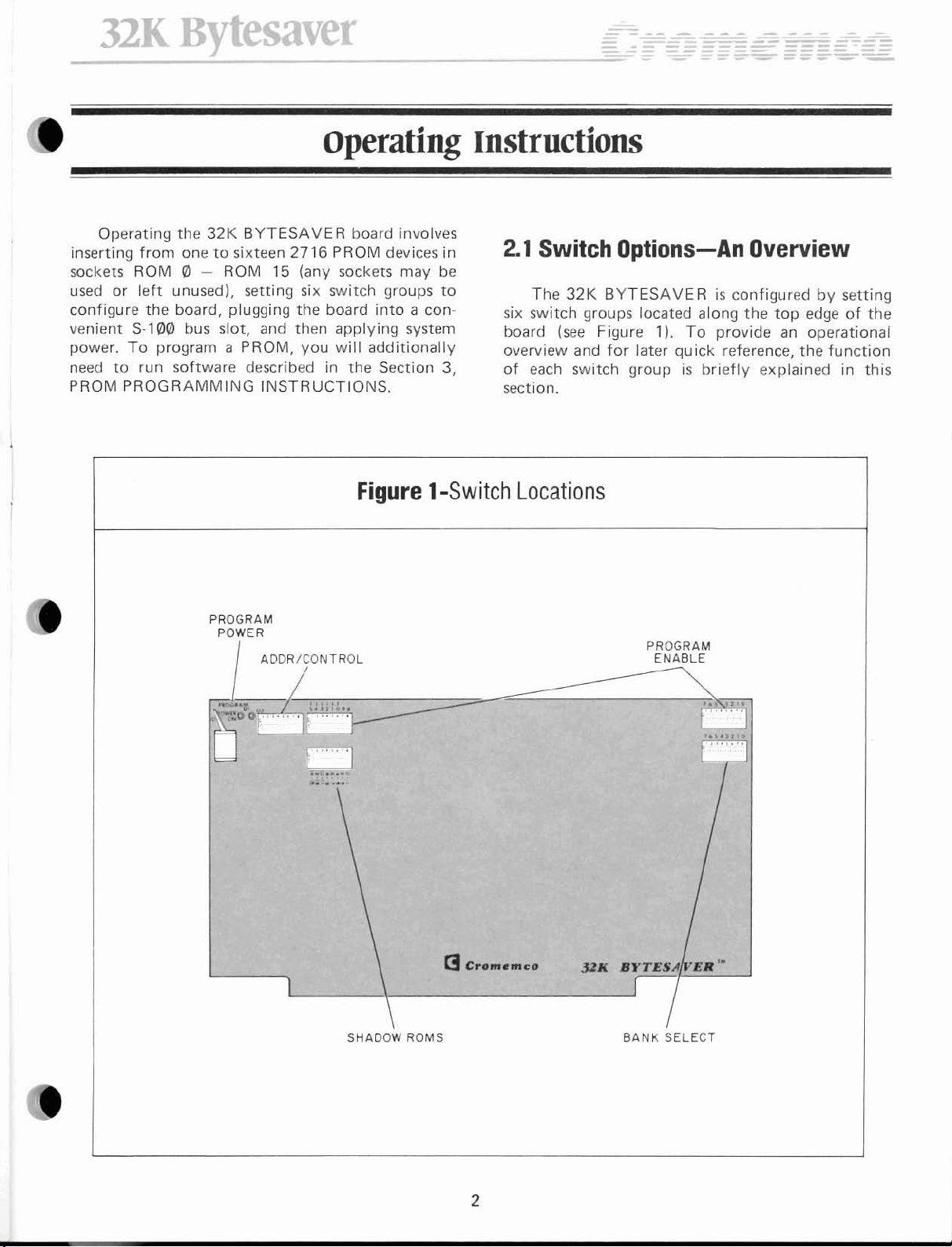
operating Instructions
- -
-
=
-~-
Operating the
inserting from
sockets
used
configure
venient 5·100
power.
need
PROM
ROM 0 -
or
left
the
To
program a PROM,
to
run
PROGRAMMING
32K
BYTESAVER
onetosixteen 2716 PROM devices
ROM
unused), setting six
board,
bus
slot,
software
15 (any sockets may be
plugging
described
the
and
then
you
INSTRUCTIONS.
board involves
switch
board
applying system
will
in
groups
into
additionally
the
Section
Figure I-Switch
PROGRAM
POWER
r--l.,
ADDR;!DNTRDL
to
a con-
in
3,
2.1
Switch Options-An Overview
The
32K
six
switch
board
overview
of
each
section.
BYTESAVER
groups located along
(see
Figure 1).
and
for
later
switch
groupisbriefly
is configured
To
provide
quick
the
reference,
explained
Locations
PROGRAM
ENABLE
top
edgeofthe
an
operational
the
by
setting
function
in
this
~
••
t .....:
I
..
..
~.....
,-
....
.
'r
...
~
SHADO\
ROMS
[)
Croon_on",o
..
..
'H
".
"
""
BI'TESA/.'ER'~
jZl<
BANK
iLEeT
2
Page 9
32K
PROGRAM
The
voltdetodepower
indicator
fore
PROM
donetoprevent
Bytesaver
POWER
PROGRAM POWER switch
ON
and
OFF.
programmmg:
inadvertent
ADDR/CONTROL
The
ADDA/CONTROL switches control several
different
multiple
ON,
direct
functions
Switches
The
and disables
64K
1, 2
BANK
64K
addressing).
and
ENABLE/DISABLE
memory
multiple
Toggle Switch
turns
supply
and
the
nearby red LED
Position this switch ON be-
position
re-programming.
Switches
(see
Figure 2).
3 are
not
used.
switch enables
banks (bank
banks
0-bank7)when
when
the
+26
it
OFF
when
OFF (normal
The
WAIT
CPU cycle
memory
switch
cycle;
When used
ning at 4
maybeleft
SAVER
address space
pOSItion IA15=0>, and
the upper
(8000H-FFFFHI
(A
15'11.
DMA
OVERRIDE
DMA
performing
access time. Positioning
ON
the
The
A 15
boardinthe
The
DMA
OVERRIDE
addressing,
STATE
time
to
the
introduces
OFF
position
in
a Cromemco system
MHz,
position
OFF
when operatingat2
switch
lOOOOH
32K
half
when
ENABLE/DISABLE
when
when
OMA
OFF.
position
with
switchisusedtomatch
2716
one
introduces
the
memory
lower
-7FFFHI
memory
of
ON
For
memory
PROM
wait state per machine
switch ON.
maps
32K
memory
in
the
and disables
normal
the
switch
banks enabled.
45005
the
WAIT STATE
no
with
MHz.
the
32K
halfofthe
when
maps
in
the
address
ON
switch
OFF.
the.
(max)
wait
states.
a ZPU runThe
switch
BYTE·
memory
the
OFF
board
direct
in
space
position
enables
OMA
64K
When
turn
Figure
~2E8-\HPJ.HI-I'
2-ADDR/CONTROL
~~---
~~==ONE
I
MEMORY
AIS=I (UPPER
DMA
r-DMA
-lH
L-DMAIN
-'===
L
_~~====
l
DMA
AIS=O (LOWER
NO
WAIT STATES
MEMORY BANKS DISABLED
NOT
USED
Switches
BAN~S
WAIT
OVERRIDE ENABLED
OUT
OVERRIDE
STATE
ENABLED
32~)
DISABLED
32KI
•
3
Page 10
32K
the
switch ON.
only
when
OVERRIDE enabled, the 32K BYTESAVER
respond
address range
by
board disabling if
current
feature effectively permits
board
banksasthe
and the boardsinother
boards
out
(the
Bytesaver
The
DMA IN/OUT switchisactive
DMA
OVERRIDEisenabled. With
directly
active memory bank statusatthe
of
ones
toaDMA
by
board enabling if
DMA
several stackedindifferent
DMA
board (the one
with
DMA OUT).
in
is
the
memory
the
board's
DMAisIN,
OUT,
usertodefine
with
banksasnon-DMA
regardless
time. This
memory
DMA
DMA
will
16-bit
and
of
one
INI.
BANK
SELECT
Switches
The eight BANKSELECT switches map the 32K
BYTESAVER
ble 64K
IOta any combination of eight possi-
byte
memory banks (bank 0 - bank
71.
Set
ting a BANK SELECT switch ON logically places
the board
bank; an
from a bank.
the numerals printed above
switches
in
the correspondingly numbered
OFF
switch logically removes the board
Again, associate
the
bank
the
on
the
p.c. board,
not
the
memory
number
with
BANK SELECT
numeralsonthe
DIP proper_
PROGRAM
The sixteen
,
vidually
ROMO
gramming;
These switches may be alternately viewed as
ORY
write operations wheninthe
To enable and disable socket programming,
associate the board socket numbers
ROM15) with the numerals printed above
switch DIPs
a
to
the
ENABLE
enable
thru
ROM15. An ON switch enables pro-
an
Switches
PROGRAM
and
disable
OFF
switch
ENABLE
programming
inhibits
programming.
switches
PROTECT switches, preventing any
OFF
position.
on
the p.c. board (15
to
the far left,
far right).
indi-
sockets
MEM-
memory
IROM0-
the
two
SHADOW
Each SHADOW
ROM
Switches
ROM
switch controls
sockets (the rightmost controls ROMe and
the leftmost controls
ing
both
sockets
switch
("floating"
ed)
SHADOW
4K-byte
space,
is
OFF, and by removing
the
from the
ROM
"hole"
into
which
memory
in
board
SWitch
In
another
ROM
the
14 and
memory
ROM
map when
both
when
either socketisaddress-
map when ON. Placing a
ON effectively creates a
the
32K
BYTESAVER address
memory
module may be
151
mapped.
two
ROM
by plac-
sockets
ROM
1,
the
4
Page 11
32K
Bytesaver
:-=0:::
==-==-
==-=-=-=-
----
Suppose
your
32K
of
memory.
program
there are
Example
you
have a
BYTESA
Asastandard
2716 PROMs
no
other
VER
boards in the
1
4MHz
(0
ZPU
and
reside in the upper
practice,
in
socket
upper
yOll decide
ROM€)
32K
Figure
ary,
so
for
wouldbeas
To
you
of
want
32t;
co
only;
memo
Then,
lings
settings remain the same
POWER switch which /IIl/st be
3-Example1Switch
multiple
memory
programaPROMinsocket
memory
read
showninFigure 3.
banks
operatioll.
except
turned
Settings
are nor required.
the
switch
ROMe,
the PROGRAM
ON. 0
all
set·
switch
PROGRAM
POjER
,---BANI<
r
'fi'
"l'L--r't"
l'~:"":;;~;=";'~:;:~1
U .
~~==
l
DISABLE
~==A1S~1
--l-
DON'r
CARE SINCE OMA
OVERRIDE DISABLED
iDISABLE
PROGRAMMING
ROM
a-ROM
t~,';";1
L
ALL
SOCKET PAIRS
IN MEMORY MAP
OMA
OVERRIDE DISABLED
ONE WAIT STATE
NOT
uSED
15
ENABLE
PROGRAMMING
DISABLE
ROMf~ROM
PROGRAMMING
DON'T CARE SINCEI
BANKS DISABLED
:UN
ROM
7 l
BYTESAJlER
0-
,.
5
Page 12
32K
The
Bytesaver
following
example
BYTESAVER special features.
Example2
uses
all
of
the
32K
program
ROM15
PROM)
lower
(assume this
four
(programming
amI
32K
PROMsata
a 16K
of
memory
card
is assignedtomemory
limeinsockets
8K
blocksofsource code
RAM
solely
- - --
-~--
-----
--
=~
card also residesinthe
for
---
;:;:;:.
DMA
bank
ROM12-
transfers
1
J.
to
Suppose
the
board
The system has
OOOOH-OFFFH,
the
32K
you
to
resideinthe
BYTESAVER
have a
4KofRAMatoverlapping addresses
so
2MHz
a
4K
memory
PROGRAM
POWER
system
lower
"hole"
32K
mustbecreated
map. You incend
Figure
r::====BANKS
I
,---DMAOUT
[[=
.-L
and
you
walJl
of
memory.
in
co
4-Example2Switch
Ar5=O
ENABlE
PROGRAMMING
,DISABLE
PROGRAMMING
ENABLED
ROM
ROM
memory
Power·Qn-Clear
details. The
settings
in
Figure 4 0
12·RDM
a-ROM
15
II
You decidetoassign the
bank
0 so
it
will
or
RESET -
for
memory
appropriate
read
32K
operations
Settings
DISABLE l
ROM
O-ROM
PROGRAMMING
7
32K
BYTESAVER
be
enabled
see
Section 2.6
BYTESAVER
oniJsystem
are
then
10
for
switch
shown
-
'--SOCKETS
L---OMA
~====NO
L
SHADOW
ROM
IN MEMORY
NOT
SOCKETS
O-ROM 3
OVERRIDE
WAIT STATES
USED
ROM
4-ROM
MAP
6
15
ENABLED
BOARD
BANKI-BANK 1
BOARD IN
NOT
IN
BANK
lIUOUUO~O
Page 13
All
32K BYTESAVER special features and operational modes touched upon above are discussed
greater detail
follow.
2.2
Addressing
Addressing a
volves four levels
bank, a memory board, an
choosing the byte-on-chip_
Memory banks are
puning
a control word
in
the sections which immediately
The
32K
BYTESAVER
byte
on the 32K BYTESAVER
of
selection: choosing a memory
IC
chip, and finally
addressed by the CPU out-
to
an integral OUTPUT
in-
PO
RT
40H contained on each 32K BYTESAV ER
in
board. Board, chip and byte-on·chip are all decoded
from the sixteen bit address seni:
the
S-l00
bus.
Since the board capacity
selectisgenerated by
A15. There are sixteen
four high order address lines A
hardware generate chip enable (selecting ROM0ROM
151.
and
the
-A
10 are used
2716
PROM (see Figure 5).
to
the
ROM
remaining eleven address lines
address one-of-2,048
out
by the
is
32K bytes. board
high order address line
sockets. so the next
11-
A14 are used
CPU
bytes
on
to
AO
on a
t
Figure
Execute OUT (40H), A } _
A15}-----
~~~j------
A12
A
11
A10
A9
5-32K
BYTESAVER
AS
A7
A6
}--------
A5
A4
A3
A2
Al
A0
Addressing
Select bank0-7
Select one-of-two boards
Select one-of-sixteen chips
Select one-of-2048
bytes
7
Page 14
32K
Bytesaver
2.3
Board
SELECT/CHIP
Select
5-100 bus address line A15ishardware com-
pared to switch A15 in
switch group. Switch A15
dress line A15""1 (address
A 15
OFF
corresponds
dresses
place
32K halfofthe
liyte
two
BYTESAVER Schematic)
to!
may
0000H-7FFFH).
the
32K
BYTESAVEA
64K address space, respectively_
Each ROM socket
swathofmemory.
one-of-eight decoders
each
ROM socket.
then
be
spanned
the
ADDR/CONTROL
ON
correspondstoad-
800eH-FFFFH);
to
address line A 15=0 (ad-
These two switch settings
in
the
upperorlower
IROM0-ROM151
Address lines A
(ICG
and
to
generate select signals
The
entire
by
64K address space
two
32K
spans
11~A14 feed
le7
in
BYTESAVER
switch
the
a 2K-
32K
boards. Figure 6 illustrates such an
along with
socket.
Suppose
with
BASIC.
EOOOH-£3FFH.
EFFFH.To
place the
ROMI2
assigned
the
address range
you
Cromemco's
The
Z-BO
load
two
and
ROMI3
to
800fJH-FFFFH
Example
programmed
Z-80
MONITOR
MONITOR
and
Control BASIC
these programs,
programmed
on a
with
spannedbyeach
3
two
and
spans
you
PROMs in
32K
A 15=1. 0
arrangement
ROM
2716
spans
BYTESAVER
PROMs
3K
Concrol
addresses
E400H-
would
sockets
then
8
Page 15

32K
Bytesaver
Figure6-Two
BY-ESAVER
WITH
BYTESAVER
WITH
32K
BYTESAVERS
A
32K
AIS"" I
A
321<
AIS=O
ROM,.
ROM
ROY 13
ROUIZ
ROUII
ROM
ROM
ROM
ROM
ROM
ROM
ROM
ROM
ROM
ROM
ROM
ROM
ROM
ROM
ROM
ROM
ROM
ROM
ROM
ROM
ROM
ROM
ROM
ROM
ROM
ROM
ROM
Spanning
"
'0
9
8
1
6
•
•
3
2
I
D
15
14
13
12
II
10
9
8
7
6
5
4
,
2
I
0
ADDRESS
(HEXI
FFH
r800
rooo
<800
<000
D800
DOOO
C800
COOO
8800
8000
>800
>000
9600
9000
e600
8000
1800
1000
6800
6000
5600
5000
4600
4000
3800
'000
2800
2000
1800
1000
0800
0000
The
64K
64K
Address
BYTES
Space
9
Page 16

32K
Bytesaver
2.4
Shadowing
A
32K
BYTESAVER
the CPU's
SHADOW
pairs of
"holes"inthe
be "filled" with
SHADOW
ated
ROM sockets:
controls
ROM15):
the
two
64K
ROM
ROM sockets thereby creating
board's
ROM
the
two
the
rightmost
rightmost sockets
ROM
direct
Socket Pairs
board spans one
addressing range.
The
half
eight
switches allow the usertoremove
4K·byte
other
switch
the
leftmost
memory
controls
leftmost switch
switch
map
which
memory
sockets
(ROM~
modules. Each
two
vertically separ·
(ROM14
(number81controls
and
ROMl). Posi-
may
lnumber
then
and
tioning a switch ON completely removes a socket
pair from the
the
socket
Suppose
System (COOS)
-7FFFH.
memory
pairinthe
you
have a
with
and
a
32K
map;
map.
Example
Cromemco
32KofRAM
BYTESA
an
4
OFF
switch leaves
Disc Opera.ting
spanning
VER
assigned
OOOOH
to
of
11
BOODH-FFFFH.
troller
monitor
board. The
-C3FFH,
ROM9.
RODS
with
EOOOH-E3FFHJ.
your
memory
not
ets.
0FFH
and
bus lines
states
are
board
program
so
leavmg a
then
Further
Cromemco's
own
8K-byte
The
required
map
Carefully
equivalenttoSHADOWING
The
32K
from
as
a result
010-017
its01output
addressed,
The
is
factory
in
RODS
partially
aswme
an
program
yO/J
SHADOW
hole
you
Z-80
and
development
sw;tch
are
showninFigure
note
that
BYTESAVER
unSHADOWED
will
actively
high.
lines when
whether
Cromemco
shipped
ROM
at
fills.
program
Monitor
you
program
settings
two
empty
drive
The32K
they are
Floppy
with
memory
spans addresses
sockets
COOOH-C7FFH
one-halfofa
program
system.
and
7.
ROM
the
will
memory
empty
all eight
BYTE5AVER
SHADOWED
emptyornot.
Disc COIl-
the
on
the
ROMS
four
2716s
the
0
sockets are
same
two
read data
ROM socket,
5-100
RODS
4FDC
COOOH
and
whIch
2716
(spanning
w;th
resulting
sock-
data
tri-
sockets
10
Page 17

32K
Bvtesaver
Figure
.
~
7-Example4Switch
~
..
"'
"""••
....
"OIO~
,.
'r::;;;'
/1
!~
"":-
Settings
:-I(l
.....
TOIl
•
And
,..
......
;/
Memory
(to
,-.n
I
Banks
••
C£.(L~"'..r
S'
......
AR[
I
/1
' ,
..
•
S.....:>.;..T:.
"-'
-('
~
.'"
~'-'"
~r,
...
~.'"
• •
"-
..
I
~.:" ~
1"_·,,
'I.."
<t.
" f
"'
....
.......
....
• W •
••
• •
C3
.,
I--
,.
•
,
,
,
~..~
I--
~
Cr
........
.'.1£'"
(OIPTf
(IlIPI,
0.'"
f
U~(~
DUI"Ll'
:'."'"'l,lVH
[WJoTl
[Ill""
L
fl-;''''I''''
"{
[
..
,,'~
(011'1.
(_T,
t.
8,'H
<
(.
"'
..
: #
.....
~
"1(
"'
_
~
...
BYT£SAJ
"'.
.uK
£R
•
r
A(,('"
f
"f
'.'
fl'
,.
LH' .,J
F'/Xl
(,~·_oo
'
....
-.
,·m
"
l
\.
tor
,.y
_
•
0
0
~
-
..,.
..
11
Page 18

32K
Bytesaver
2.5 Memory Banks
BANK
which
the
CPU's
may
BANK
group. When thisisdone. the eight
switch settings
32K
BYTESAVER
half
of
memory
tions.
SELECT
effectively
64K
be
completely
DISABLE
the
CPU's
read, PROM
is
an
optional
allows
memory
direct addressing range. This
in
become
exists
64K
disabled
the
irrelevant. In this
direct
programmingorDMA
by
ADDR/CONTROL
only
in the upperorlo
addressing range
board feature
expansion
switch
BANK
beyond
feature
selecting
$\'\Iitch
SELECT
mode
.....
opera-
the
er
for
To
enable memory banks, switch select BANK
ENABLE
When this IS done,
ly placedInone or more
with
addressing IS
OUT
Memory
(see
SELECT
each
hand,
in
the
ADDR/CONTROL
the
32K
the
eight BANK SELECT switches,
software
(40H),A
Figure
correspondmg
positioning
(or
may
81.
switches
controlled
equivalent)
be
stacked
Positioning
ON
placesa32K
memory
all
switches
switch group.
BYTESAVERislogical-
64K-byte
Z-80
uptoeight
one
bank.
memory
by
executing
instruction.
or
more
BYTESAVER
On
OFF
completely
and
banks
the
banks
bank
deep
BANK
other
the
m
reo
Figure8-
16-BIT
FFFFH
The
Memory
32K
BYTES
Map
With
Multiple
Memory
SIZK BYTES
TOTAL
Banks
ooooH
BANK 7
BANK6
I-
BANK"
BAN)'. 3
BANK S
32K
BYTES
I-
BANK 2
L
BANK I
---.lBANK
12
0
Page 19

32K
Bytesaver
-----
.
- - ::
--
~
--
-::.=.
moves the board frorn
sibly
for
DMA
transfers -
As
stated
and deactivated
BYTESAVER
40H
which
put
toitby
its corresponding
(logic01disables its
controls
above.
contains
latches
the
memory
under
the
CPU. Each
memory
bank
bank 6, etc.
the
memory
see
memory
software
an
bitsofthe
bank.
Control
7,
map (except pos-
Section
integral OUTPUT PORT
set
bank, and each reset
bit6controls
Figure
BOARD
2.7).
banks
bit
are activated
control.
control
(logic11enables
byte
Each
bit
9-Example5Switch
AOOR/CJJt~""ROL
a /
~
=
-t
32K
byte
Qut-
7 (MSBl
memory
t
""
bit
,
'I
If
the
32K
anyofthe
calOR).
thusisplaced
condition
Conversely.
mapped
byte.
trol
and
ed
control
indicator
responds
banks activatedbythe
the
occurs,
into
the
thusis"out"
byte
goes
by
Settings
BYTESAVERisswitch
control
board
if
no
board
inactivates
out,
tri-statlOg (floating) all
"in"
the
bank
responds
the
the
green LED
32K
activated
will
of
and
when
memory
BYTESAVER
by
not
respond
the
memory
the
board,
more
specifically,
BANK SELECT
\
mapped
byte
addressed and
map. When
indicator
is
the
output
when
address-
map_
When a
the
green LED
the
of
its
output
f\
'.
into
(Iogi· •
this
lights.
switch
con-
board
-AI5=1
L-SANK
ADDR/;ONTROL BANK S,ELECT
~B~O;A~RD~A:;!~
~5:or
/~;;;;:;;-..L
o'~r
l..--AI5=1
L--BANK
"'I
t .
..
'I
ENABLE
ENABLE
n«
I
--':
IN
BANK
_,rESAIE_·
I
\F""'''j
L\.--'
, ,
r,
accr~
UK
...
0-
Bt'r£SAlt'liR
,~
•
13
h
Page 20

32K
Bytesaver
lines.
boards
This
with
behavior
BANK
allows
SELECTtooccupy
two
overlapping 16-bit address space
memory
activeata time. and all
Memory
banks. provided
bank
al
Two
conflicts
or
more
only
one board is
other
may
address overlapping
boards are inactive.
result
boards are switch assignedtothe
ory
bank,
or
b)
Two
or
memory
more
boards assignedtodisjoint
16·bit
address overlapping
or
more
the
but
in
if:
Figure
memory
same
or
different
memory
memory
same mem-
Suppose
mapped
and theIr
Figure9.The
memory
In
Figure
ID-Example5Memory
banks are
simultaneously
samt! control byte.
Example
two
32K
mto
the
upper
memory
10.
bank switches are setas shown in
rewlting
memory
Map
activated
5
BYTESAVERs
32K
of
memory
mapisthen
by
are
fA
75~1).
shown
the
both
ADDRESS
16-BIT
FFFFH
ooooH
~'-----
r-l~~~~~~~~l~
BOARD A
BANK 7
BANK
6
BANK 5
~
BANK
4
f- BANK 3
f- BANK 2
BANK
L
.J8ANK
I
0
14
Page 21

_
3_~_K_B....::yte_sa_~_e_r
To
•
Executing
and
instructions
memory
3,
banks
continue the
the
and
de-activates
then
(both
same
example. the sample programs below illustrate how to
memory bank enable and disable the two boards.
instructions
place
boards
both
below
all
inaccessible).
other
board
activates
A
and
~:::.---
-
memory
memory
board
banks.
B
-:_
----------
banks
in
inactive
-~;~
2
The
-;.-
•
ADDR
0000
0002
0004
'*
Executing
both
'*
active
(board
transfers;
boa
AODR
0000
0002
0004
Executing
OBJECT
3E0C
0340
cds
OBJECT
3EB1
0340
memory
A
available
board
A
the
the
MNEMONIC
LD
OUT
instructions
and
B,
MNEMONIC
LD
OUT
bank,
B
A,"""011008
(40H) ,A
and
thus
A,10000001B
(40H)
instructions
and
for
inaccessible).
board
memory
,A
below
is
illegal.
below
B
read,
COMMENT
;LOAD
;OUTPUT
;NEXT
simultaneously
COMMENT
;LOAD
iOUTPUT
iNEXT
places
in
an
inactive
PROM
0000
INSTRUCTION
1000
INSTRUCTION
programming
1100
CONTROL
0001
CONTROL
board
memory bank
INTO REG. A
BYTE
activates
INTO REG. A
BYTE
A
in
and
TO
TO
OMA
PORT
PORT
an
40H
40H
ADDR
0000
0002
0004
*
Executing
inactive
(board
PROM
ADOR
0000
0002
0004
OBJECT
3E01
0340
the
memory bank and
A
inaccessible;
programming
OBJECT
3E60
0340
MNEMONIC
LD
OUT
and
MNEMONIC
LD
OUT
A,00000001B
(4I3H)
instructions
board
OMA
A,01100000B
(40H)
,1>.
board
B
transfers).
,A
;LOAD
;OUTPUT
;NEXT
below
B
in
available
;LOAD
iOUTPUT
iNEXT
15
COMMENT
0000
CONTROL
INSTRUCTION
places
an
active
for
COMMENT
0110 0000
CONTROL
INSTRUCTION
0001
board
INTO REG. A
BYTE
A
memory bank
memory
INTO REG. A
BYTE
0
TO
in
read,
TO
PORT
an
PORT
40H
40H
•
Page 22

_3_~_K_B-:.yt_e_s_a_ve_r
----=~:-
_
=~
=::
:;~
-
~
2.6 Select BANKB
On
RESETOrPOWER-ON-CLEAR
When system powerisfirst applied,orafter
subsequent system RESET,
will
respondinoneoftwo
SELECT is DISABLED, the board will remain
the
memory
addressing range.
If
BANK
o is automatically hardware activated
RESET
through 7 are de-activated. Thus. a RESETora
to
the
boardsinExample 5 would activate board A,
and
de-activate board
2.7
Direct
A device may request direct
the 32K BYTESAVER by asserting the 5-100 bus
•
line pHOLD low.
driving line
control line pH LOAishigh,
directly drive the
trol lines (which are tri·stated during
map
in
SELECT is ENABLED,
or
a power-on-elear (POCI. and banks 1
B.
Memory
The
pHlDA
(hold
S.100
the
32K
BYTESAVER
different
the CPU's 64K-byte direct
ways.IfBANK
memory
by
a system
Access
memory
CPU grants
acknowledge) high. When
the
device
bus
address lines
the
DMA
access to
request
then
and
transfers
a
"in"
bank
poe
by
may
con·
when pHLDA
for reading
The
device may
only
by
the
The general features
• Fast asynchronous read
memory.
• The DMA device should
for many overhead tasks (such as
bank switching)
as quick as possible.
•
The
slow
• The
ling
and
In
line with this general philosophy.
BYTESAVER's DMA response behavior
led
by
two
switch group;
There
tions; each
are four possible switch setting combina-
is
high),
or
writing
then
memory
accessisdirect - no CPU intervention to
the
transfer.
DMA
device mustbecapableofcontrol·
and
driving the tri·stated address,
control
is
busses.
switches
DMA
tabulated
and
use
without
transfer
access time.
ofaDMA
to
keep
in
the ADDR/CONTROL
OVERRIDE
and
discussed below.
the
data
CPU intervention.
dataata rate limited
transfer are then:
or
write access
not
be
the
memory
and
DMA IN/OUT.
bus
lines
to
responsible
memory
access
data
the
32K
is
control·
DMA
OVERRIDE
SWITCH SWITCH
DISABLED
ENABLED
ENABLED
Table 1
DMA
IN/OUT
INorOUT Board enables when correctly addressed
OUT
IN
32K BYTESAVER
for
either
Board enables when correctly addressed
for non·DMA transfers (normal operation);
board disables during
transfer.
Board enables
for non-DMA transfers; board enables
the
assigned 32K blockofmemory,
of
which
request_
DMAornon·DMA transfers.
when
oMA
device addresses
banks
were active before the DMA
RESPONSE
any
system DMA
correctly
the
addressed
board's
regardless
when
16
Page 23

32K
The
first
ior
with
DMA OVERRIDE DISABLED
this case the
vant). Here,
32K
the
read,
only
tiple
address faits
BYTESAVER
write
when
memory
Bytesaver
table
entry
indicates
DMA
the
(PROM
it is
within
IN/OUT switch settingisirrele-
key
phrase is
programming)orDMA
in
an active
banks
are
the board's
"correctly
will
respond
memory
enabled).
assigned
the
and
board
bank
the
behav-
(note
that
addressed";
for
memory
transfers
lif
5-100
32K block
in
mul-
bus
of
memory.
tiate
between
read/write
The
tween
OVERRIDE
table entries. A
how
DMA
The
cycle in
32K
DMA
ENABLED.
OVERRIDE
boardineffect
a
DMA
BYTESAVER
and
typical
data
any
way.
non-DMA
works
-===-.:.==
does
not
transfer
does
transfers
as
shown
application
is showninFigure 11.
and
differentiate
with
in
the last
demonstrating
---.--
---
differen-
a normal
OMA
two
be-
AooA/ONTROl
~Jl
..
l..-.--MEMOAY
Figure
..
" ,
" , .
,.
, ,
,
-oMA
~DMA
L..-AI5=1
ll-DMA
AoDRiCONTROL DMA
~'
'.
".
OUT
OVERRIDE ENABLED
BANKS ENABLED
OVERRIDE
:.
~:~
-OM
-AI5=1
DISABLES DURING
DMA
.
')
I!
MA
IN
A OVERRIDE ENABLED
MEMORY BANKS ENABLED
TiNSFERS
/
Example
RESPONDS
/
BANK
BOAROA
Configuration
TO
iOUESTS
BOARO B
,lEeT
t\'
I"",,~=il
ll.
,
BANK SELECT
.
1\'
fa..,:~;~~
B"Tl:SAV~R'"
[
CJ
Cr
......
e.
I
.uK•.,T£SAJ'I!.·
I
17
•
Page 24

32K
Here,
,
the
same
Board Aisassignedtomemory
to
memory
boards
could
transfers,
,
•
operations
memory
isinmemory
quest
automatically
the 5-100 bus address is
with
also be used in the example).
When
by
Bytesaver
two
32K
BYTESAVERs
16·bit
both
bank
the
address space
bank
1 (any
BANK
when
bank 1at8000H-FFFFH).
driving
SELECT
boards are available for read/write
correctly
" at
8000H
CPU grantsanasynchronous
the
pH LOA line high,
disables
and
with
other
and
addressed (board Aisin
- FFFFH and
board
in
are assigned
the
A15 switch.
bank0.and
Cromemco
DMA
OVERRIDE
For
B enables
the
range 8000H _
board
memory
non-DMA
board
DMA
reo
board
when
to
FFFFH,
B
B
A
memory
means
ies during a
of vectoring the
one
boards
ing the
bank switching responsibilities.
completed.
the
the
regardlessofwhich
bank
before
Thus, the
of
with
!the
It should
same memory bank
DMA
DMA
overriding logical memory bank boundar·
DMA
DMA
ones with
DMA
be
both
transfer.
the
OVERRIDE featureisseen as a
transfer. This provides a fast way
DMA
IN)
device
noted
32K BYTESAVERs revert back
board
request.
devicetothe
and disabling
DMA
OUT)
with
any
that
after
the
status
which existed before
wasinan active
DMA
board
all
without
overhead memory
DMA
(the
non·DMA
burden·
transfer
to
is
I
I
I
I
•
18
Page 25

•
Page 26

32K
Bytesaver
- - -
--
----
.=
-
==
PROM
Programming Instructions
•
The
2716
erasable
memory
bitstothe
parent
tion. Consult
detailed
The
tially.
EPROMs which mustbeprogrammed sequentially).
The
changing
Note
changed
only
tion.
BYTESAVER socket with the system power
turn
GRAM ENABLE
remove the boardorboard parts while system power
is
ON). The 32K BYTESAVER hardware then permits you to program a 2716
fonning
by executing
commands
32K BYTESAVER senses the
forces the CPU
until
the
data
PU
LSE.
50
msec, thus the entire
in
approximately
seconds.
Specific
the
to
program
Z-B0 MONITOR system commands, Section
cusses programming using 3K Control BASIC.
Section
Z-80 Assembly Language code.
and
chip.
quartz
erasure
The
2716
bytes
orinrandom
bits
in a
logic 1 (erased)
that
from
complete
To program a
ON the PROGRAM POWER switch
a
byte
2716
with the target address
byte, then applies a digitally timed PROGRAM
Programming
2716
next
three sections. Section 3.1 illustrates how
3.3
is a
electrically programmable read-only
The
logic 1
window
the
procedures.
is programmed
maybeprogrammed
byte
bits
the
EPROM erasure can force this transi-
memory
anyone
describedinthe following sections). The
to
programmingiscomplete, property drives
programming examples appear
2716s
deals with programming 27165 from
16.384-bit,
chipiserased,
state,byexposing
to
intense
2716
manufacturer's literature for
order
are
may
logic 0
2716,
the
write to
an idle
2,04B x
using
(contrasting
programmed
bits
not
backtothe
insert a
ROM
socket (never insert
the
of severill Cromemco system
state
one
byte
2716
50
Cromemco's
ultraviolet
thereby
the
ultraviolet
one
byteata time.
individually. sequen-
by
to
the
logic 0
be
programmatically
logic 1
2716
byte
by
target location lor
memory
via
takes approximately
may
msec or
write cycle,
the
and
the program
be
programmed
chip's
with
selectively
into a 32K
and
merely per-
pRDY line
about
RDOS and
light
forcing all
transradia-
earlier
state.
state-
OFF,
PRO·
or
100
in
3.2
dis-
and
3.1
Programming
From
Iy,
above. Thus,
as a
vided a
o
move,
used
mands
memory) will
the
2716
since a write cycle
50
familiar With either Cromemco's RDOS
MONITOR programs.
follow,
residing
move
where
RODS
The
2716
sequentially
true
wnte
bit
to logic 1 bit. All system
substitute
to
program and verify 27165_
which
system
(e.g.•move memory) will slow significantly
msec instead of
It
is
assumed
itisalso assumed
a)
An erased
ROM15
been mapped into the
(A
es
b)
The
positioned ON.
e)
Socket
ABLED.
dl The userisin
TO R and has just been
command.
To program the
at
memory
M
400
or
M
400
<CR>
Dr
l-BO
bytes
or
in random
the
2716
readlfastl/writelslow)
cycle never
or
memory
be
executedatfull system speed,
commands
to
750
that
2716
on
a 32K BYTESAVER which has
15= 1), thus the erased
F800H -
PROGRAM POWER switch has beer'
FFFFH.
ROM15 has been PROGRAM
Example
400H
BFF
SBf)(I
- OBFFH.
command:
FBO/KCR>
FBOO<CR>
stands
for
MONITOR
maybeprogrammed individual·
orderasmentioned
may be properly
memory
attemptstochange a logic
commands
display
the
either
memory
read the
which
2716
nsec (with a 4
a reader
In
that:
has been insertedinsocket
2716
memory
takes
approximately
of
this section
both
examples which
upper
RODSorZ-80 MONI·
32K of
2716
spans address-
prompted
6
entire
2716
you
pressing the
with
would
RETURN
thought
chip, pro-
which
may
then
System
(e.g.•display
writetothe
MHz
source code
com-
clock).
or
Z-80
memory
for a new
issue the
key.
of
be
but
is
EN-
19
Page 27

32K
AllY
the
programmed
are discrepancies,
Bytesaver
discrePilocies
between
2716
you
willbeprinted
should
che
source code
again
ilnd
out.Ifchere
tum
ON
the
PROGRAM POWER switch, and re-program the
2716
above, or
tratedinthe
FCOOH,
B8H,
2716
of
accomplished using the substitute
mandasillustrated
acters
with the move
memory
commandasshown
use the substitute memory command illus-
lJext eAampJe. 0
Example
Assume
89H.
is assumed erased. the current contents
these locations is FFH. This task is
you
FCDIH.
BAH
wane
FCD2H
and
to
88H
program
amI
FC03H
respectively.
7
2716 addresses
with
memory
you
SM
FCOO<CR>
FCOO:
below.Inthis
type
are underlined.
FF.BB FF.B9 FF.8A FF.8B
example.
data bytes
Since
of
each
most
easily
com-
the
char-
FF.<CR>
the
To
SAVE a
a)
Determine
text using
b) PROGRAM ENABLE sockets containing
erased
cl
Turn the PROGRAM POWER switch ON.
d) Issue a SAVE
is
e)
After receiving a
successful programming,
GRAM POWER switch OFF_
3K Control BASIC logically partitions memory
into "pages", where 1 page
IOOOOH-01FFH)
1
3 I0200H
buffer and the stack; pages 4 thru 31 10400H -
1FFFH)are normally used for
arrays; and pages
are normally usedtosave
ure 12).
the
2716
-
03FFH)
CB
programina
the
length of
the
CB
SIZE function value.
2716
PROMs.
ppp
PROM starting
are
not
are used for variables,
32on12000H - end of user
2716
the
command
"page"
CB
message indicating
turn
=
256
bytes.. Pages 0 and
usedbyCB; pages 2 and
CB
program text and
CB
program files lsee F
PROM;
CB
where
address.
the
the
program
"ppp"
PRO
input
RAM)
ig-
If
you
then
properly
display
OM
wantedtovenfy
programmed
memory
FCOO
command:
FCD3<CR>
the 2716,
that
you
the
would
or
OM
FCDD
S4<CR>
and the response shovld be:
FCOD:
88 89
8A
88
Tile Z·80 MONITOR program svpports a PRO·
GRAM commancl
2708·type
command).
EPROMs (RODS does
While
program 27165,
execute due to tile
to program
3.2
from
3K Control BASIC
stored
execution
SAVE
CB
program text area
the
2716isfunctionally equivalenttoa readlfastl!
writelslowl RAM, the SAVE
used
to
tile 2708. 0
Programming
3K
Control
in
2716
by
commandisnormally used for moving
program
which
is
designed to program
not
support this
in principle the command will
ill
practice it will take hours to
large
numberotpasses required
BASIC
(CB)
program
PROM for subsequent loading and
issuing
2716
the
SAVE command.
to
RAM
command
PROMs.
memory,
text
may also be
four
issue a
may be
but
bytes
The
the
since
The
SAVE
CB
program text as a file for later execution, and
the LOAD
back into the text area for editing.
The
page number argumentsofthe
and LOAD commands are specifiedindecimaL For
the SAVE command, the
ing
address of an erased
erased PROM should
all
of the
fill
more
theln
2716, the
later with
To
determine the
clear the
execute the
uates and
SIZE function evaluates
allocated to,
text.
>1
PRINT SIZE
>2
STOP
>RUN
7142
The
output
gives the size of the unfilled
number should be recorded for later reference.
ppp
commandisused
ppp
command
start at this addresstocontain
CB
program text.Ifthe
7 pagesofan 8 page capacity 2K-byte
unprogrammed
CB
program textorother
text
area with
CB
program shown below which eval-
outputs
but
the SIZE function value. The
left unused, by
(7,142 decimal
brings
page argumentisthe start-
2716
2716
pages may be filled
CB
program text length, first
the
NEW
to
the
CB
to
the
SAVEd file
SAVE,
PROM. Sufficient
CB
text does
data.
command, then
number of bytes
the
CB
in
this example) t
text
buffer. This
store the
RUN
not
program
The
..
20
Page 28

32K
Bytesaver
-=.==
----
-
;'"
- - -
::::-:=...
---
;
~
--=-=-=
--
--
•
Figure
ADDRESS
FFFFH
COOOH
8000H
12-Control
BASIC
Memory
32-255120H-FFHI
Map
PAGES
•
400QH
2aaOH
OOOQH
I--
CB
FILES
CB PROGRAM
TEXT
AND ARRAYS
C=======::l I
)
,."
0-3
10'H
IFHI
(OQH-03H)
21
Page 29

32K
Bytesaver
, -
sizeofthe
LOCK
the
trol BASIC
To
load
your
this purpose),
resultinginan
unfilled
ppp
test
command
Instruction
determine
the
same
the length
two
statements
program lIeave line
then
RUN
output
like
buffer
(see
Manual).
numbers
the
that
may be changed using
Cromemco's
of
any
at
the
3K
CB
program,
beginning
Con-
of
1 and 2 free for
combined
shown
program
below:
>RUN
5938
The
program
these two numbers. or. 7142 - 5938 = 1204 bytes
=
4.7
pages. A
5ofthe
for
other
2716's
CB
Suppose
byte
CB
program in
= 9.8 pages,
the
teJ<.l.
Assume
GRAM
32K
memory
FDfJDH-FFFFH,orpages
decidetoplace the CB program
of
six
switch
ENABLE
BYTESAVER
fAI5=1J.
the PROMs on pages 24{) - 249, leaving the last
pages
250 - 255 free
would
You
ON,
and
text
length is
4.7
page program will
8 page
program
capacity,
text.
Example
you
wantedtostore a
2716
t\.Vo
2716 PROMs are
two
erased PROMs occupy PRO-
sockets
assigned
The PROMs then reside
then rum the
issue the
leaving 3 pages free
8
PROM. Since
ROM14
to
240-255
"towards
for
1<1ter
programming.
PROGRAM
command:
the
difference
then
occupy
2,500
(decimal)
2,500
neededtostore
and
ROM15ona
the
upper
32K
decimal. You
the
POWER
of
bytes
of
front"
at
may
try
to
re-program them
240
command
erase them
POWER
BYTESAVER
8FFFH
ROMO and
ABLED
run
Or,tobring
ing,
PROM
Whileinprinciple
2716
it
would
switch
Assume
or
to
the
program,
>RUN
type:
>LDAO
3K
Control
programming
devices.inpracticeitshould
take hourstoexecute.
without
and
try
again
after
now
you
sockers ROMO
pages
prevent
128
ROMI
the
128
inadvertent
issue the
program
128 0
BASIC
this
damage
programming.
move the
- 143}
should
also supports a
command
command
with
to
Turn
OFF
the
two
PROMsto32K
and
ROMI
for
running. Sockets
be
PROGRAM
re-programming. To
command:
into
the
text
- EPROM
will
not
3.3 Programming
From Z-80 Assembly
Moving
memoryto2716
ed
using RDOSorZ·80
section 3.1).
desirabletoprogram 2716s
YOllr
own
tion
discusses a relocatable
example program which may easily be
meet
your
individual
EPROM is
but
there may be instances whereitis
2-80
assembly language program.
spe<;ific requirements.
Code
bytes
or
most
MONITOR
during
Z~80
blocks
easily accomplish-
commands
the
assembly language
another
the devices,
area
also
be used since
execution
SA
PROGRAM
fBODDH
for
2708-type
program
of
system
This
modified
VE
or
-
0/5-
edit·
ppp.
(see
of
Set-
to
..
>SAVE
The
programming
page,
so
message:
SA
OK
>
if
the
programmed
SORRY
OK
>
if
they
240
timeisapproximately
after
about
VEO
ON
PAGE
PROMs
did
not.Ifthe PROMs
130 seconds, yOll
""FO
TO
""F9
verified
correctly,
do
13seconds/
would
not
verify,
see
or
the
you
Assume
with
source code located
l000H
and
you
a
2716
SA VER assigned
Thus. the
source
gion.orFCOOH-FFFFH.
a
subroutine
starting
byres
in
The
subroutme
success/ul
you
- 13FFH. This represents
decidetoload
residinginsocket
2716
code
will
whichiscalled
address in
BC
and
verification;
22
Example
walJttoprogram
the datainrhe
10
the
residesatF800H-FFFFH,
program
HL,
the EPROM $tartingaddressinDE.
returns
fA}=FFHifnot_ 0
9
and
verifya2716
in
system
ROM15ona
upper
the
upper
The program is
with
the
numberofsource code
with
fA)=DOH
memory
lK-bytesofdata,
upper
32K
32K
of
half
the source
half
BYTE·
memory.
and
of
this re.
written
code
indicating
at
of
the
as
Page 30

•
32K
--
;
Bytesaver
-------
MAIN PROGRAM
Main Program
-----
::':=
-
~
;
~~00
0003
~~06
0009
000C
;
;
;
;
This
PGM2716
(1000)
(~3FF)
(FC~0)
21~01~
01FF03
110~FC
CD0D0~
76
This
ENABLED
Switch
turn
sample
subroutine
it
CALL
RETURNS
main
which
SOURCE,
SWATH,
EPROM:
MAIN:
does
CALL
program
the
EQU
EQU
EQU
LD
LD
LD
HALT
Subroutine
SUBROUTINE PGM2716
programs
sockets
the
PROGRAM
OFF
subroutine
with:
after
on
a
POWER
execution.
with:
Cromemco
CALLs
2716
HL,SOURCE
BC,SWATH
DE,
PROM
10~~H
3FFH
~FC00H
EPROM
PGII2716
PGM2716
2716
switch
EPROMs
32K BYTESAVER
(HL)=source
(BC)=source
(DE)=EPROM
(A)=00H
(A)=FFH
(BC),
subroutine
programming.
;SOURCE
;LENGTH
:EPROM
CODE
OF
PROGRAMMING
;LOAD SOURCE START
;LOAD SOURCE
;LOAD
;PROGRAM
;END
ON
before
if
if
(DE)
PROGRAM
THE
OF
SAMPLE
occupying
memory
running
code
code
programming
successful
any
and
starting
length
byte
(HL)
START
SOURCE
LENGTH
START
PROM
MAIN
PROGRAM
start
verification
does
changed
ADDR
CODE
START
ADDR
ADDR
board.
program,
address
address
not
verify
0000
000E
0010
0011
0012
0013
0014
0016
0019
001B
0010
001E
0020
The sample progriJn) consistsofa
which
Your
,
(DE)
city.
bled
CALLsthe
mam
and
the
withaDOODH
CS
EDB0 LDIR
Cl
2B
IB
1A
EDA9
E21E00
2BF7
3EFF
C9
3E00
C9 RET
EPROM
program
(HL)
before
main
and
PGM2716,
VERIFY:
ERROR:
EXIT:
programming
must
define
calling
subroutine
starting
address. The code
PUSH
POP
DEC
DEC
LD
CPO
JP
JR
LD
RET
LD
main
segment
subroutine.
register values (BCI.
PGM2716.
programs are
For
simpli-
assetll-
may
BC
BC
HL
DE
A,(DE)
PO,EXIT
Z,VERIFY
A,-l
A,0
be
absolute
assembledtopoint
user's
verification
priate
23
iSAVE
;BLOCK
;RESTORE
iADDR LAST SOURCE
;ADDR LAST
iEPROM
;COMPARE (A)
iTHRU VERIFY
iNOT
iERROR:
i0FFH
;
SUCCESS,
; 00H
re-Iocated
,ump
responsibility
action.0
THRU:
AND
AND
anywhere
instruction
after
the
SWATH
MOVE
BYTE
LOAD
to
ON
SOURCE
SWATH
EPROM
TO
TO
IF
NEXT
(A) WITH
RETURN
LOAD
RETURN
elseinmemory
"JP
the
new
to
test
Reg_Afor
RETURN
STACK
TO
TO
BC
BYTE
BYTE
ACC.
(HL)
(BC)=00H
BYTE
(A) WITH
provided
PO.EX/T-
EXIT
point.
a successful
and
take
EPROM
is
ItISthe
the
appro-
the
re-
Page 31

•
Page 32

32K
Bytesaver
-----------'-
--------
-
-~=~
==-=
=s:=-
==::.-
=~
Theory
•
This
section
32K
BYTESAVER
user may
shooting
standing of the
functionally
plies. addressing,
cycles
4.1
32K
unregulated +18 volt line. and a Zener regulated +26
volt
unregulated
regulators. Each
one-half
volt lineisdctodc
•
ation
cuitry.
PROGRAM POWER switch,
red LED indicator.
ply the
the
and
PowerSupplies
There
are
BYTESAVER;
line.
The+5volt
of
oscillator
The
2716
gives a
find
the discussion useful
board,orjust
board's
divided
memory
DMA cycles.
four
Hnes are derived from
+8
volt line
+5
the board loads. The
01
converteristurned
prograrnming voltage.
summary
at
the
for gaining a fuller under-
features.
into
five categories:
read cycles.
major
power
two
regulated +5
with
volt line drives
convenedto+26
thru
05,
which
The
+26
volt lineisusedtosup·
discussionofthe
component
The
memory
supply
the$-100bus
two
7805Ievoltage
approximately
unregulated
volts by relax-
T1
and
associated cir-
ON
and
also
discussion
volt
level.
The
for
trouble-
power
lines
OFFbythe
controls
sup-
write
on
the
lines, an
+18
the
of
operation
is
sion
IIC16
tive
cycle.
decoders
signals for each
ed
finally select
IC7 are logically ANDedbypairs IIC5
the
these ANDed
eitherofthe
level from IC6orIC7,
and
closed lON), BOARD ENABLE will go low
disabling
BOARD ENABLE
(siN'fA)
(MEMR
IsWD OR PROGRAM POWER)
ADDRESSED ROM NOT SHADOWED).
The
board
aboveistrue,orevaluatestologic1.The
pin
memory
Address
address
Negative
SHADOW ROM
if the
AND
DISABLE)
willbeenabled
81
will be
bank.
lines
IC6
and
of
lines
A0-A9
the
byte-on·chip.
true
outputstonode
socket
corresponding
the
board.
= IA15 =
I.oUT)
low
or
has DMA
All
- A14feed
IC7
which
the
sixteen
chip
select signals from IC6
switches
pairischip
the
AND
AND
(Iel6
when
when
the
generate
ROM sockets. Buffer-
parallel feed all
parallel
BOARD ENABLE.
selected with a low
AND
output
SHADOW ROM switch
switch
IN
A15) AND
IsINP)
PIN
AND
the
logic expres-
boardisin an ac·
during
two
one-of-eight
chip
and
connect
will go low;
B)
a DMA
2716s
IC8L
AND
AND
ITHE
line
select
to
and
and
all
of
If
is
thus
If
+26
voltsisnot
PROGRAM POWER switch
torof01
at
between
age
is
the
other
volt 3%
shorts.
4.2
High
switchA15
(IC21
logically
I signal
nal
BOARD
following Boolean
for a 0
100
present,
check
converter
Zener
Addressing
order
in
pins9and
ANDed
(le16
pin
ENABLE
present
\'olt/+17
and
200
components
diode),
address
the
101.
with
81
to
expression:
volt
KHz.Ifno
01.If01isgood,
06
line A
ADDR/CONTROL
The
5-100
yield
which
across C3
is
ON, check
square
and
15iscompared
comparison
bus
the
important
logically equals
wave running
switching volt-
02-Q5,
Tl
for
signals
when
thecollec-
then
check
05(a25
opens
group
output
and
board
node
sig·
the
or
to
at
the
The
boardismapped
memory
put
address lines
IC13
with
ENABLE
ABLE'
ABLE)
LECT ENABLE
pin
system RESET!.
is
low,
bank
D·inputishigh
is
into
out.
are invertedbyIC14
bank
port
40H.
and
IC19.
control
to
I.oUT)
AND
3) lit
The
is
the
and
an inactive
bitsofthe
by
outputtingacontrol
Port
A0
- A7
These
signals sOUT,
yield
node
AND
(A0
- A7 =
strobes
also
strobed
and
boardismapped
the
green LED
when
memory
control
and
into
address
by
outputs
pWA
signal BANK
(pWR)
40HI.
the
on
a Power·On·Clear
if
the
D·inputat[IC15
into
indicator
strobed.
bank
byte
IC18.
an activeorinactive
wordtoout·
40Hisdecoded
the
wire-OAed
are logically
and
switch
SELECT
AND
A h;gh
D-type
flip flop rlC1S
an active
lights.
the
boardismapped
and
the
outputtoport
and
those
ANDed
(BANK
BANK
memory
LED
bits
7405's
BANK
pin
select·
from
and
If
40H
EN·
EN·
SE·
a
2]
the
goes
24
Page 33

32K
Bytesaver
---
---
--
-~
----
--
----
===~
-
-
ed
with
the
BANKSE
ANDed
logic 1
switch
the boardinan
to
drive
control
connected
active
bit
4.3 Memory
The
CPU
begins a memory
the
memory
A
15
and
After
CPU
pDBIN lineifmemoryisready.orthe
pies
switch
linetothe
ed with the switch, flip flop
goes low during pSYNCatthe
cycle !forcing pRDY
one
read
ANDed with BOARD ENABLE to yield signal
READ
ABLE). READ ENABLE
drivers IC27 which place the
the01bus.
32K BYTESAVER by first placing the
on
control signals
CPU then places the data
000-007,
the pRDY line.
memory has
waits an integral
address.
again goes high.
high. program
ENABLE clears PROGRAM PULSE
and
by the 2
sampling the
the
memory
strobes
017
with
the
is
not
ready.
If
no
machine cycle later when pSYNC = low.
When the CPU asserts pDPIN high
data
4.4
Memory
The CPU begins a
the
The
IC29. These dual
address
by
asserting
IS ready
the
a
momentary
pRDY
in
ENABLE'
S·100
data
coincidenceofMEM
line
wait
states
the
ADDR/CONTROL
CPU stays high; if
from the
address bus A0 - A15
sWO
asserts the
If
not
number
and
execution
MHz
CLOCK line,
LECT
the
D-inpul
output
to (IC14 pin 11) will then place
memory
Read
on
the
pRDY
to
data
from
one
are selected
= lowl. then goes high again
01
IpDBIN) AND (BDARD
switches are logically
of
to
bank.
[le15
port
pin
2].
40H which
Any
Cycles
read
cyclebyplacing
the
5-100 address bus
sMEMA
linetoascertain
supply
high transition
clock
bus. this signalislogically
in
control
the
data
the
data
in
CPU re-sam-
cycle
laterifmemory
with
group,
one
wait
stateisselect-
output
beginning of the read
turn enables tri-state
2716
[IC15 pin
to
data
A0-
line high.
whether
byte,
the
bus
010
on
the
the
WAIT
the
pRDY
81
strobe the
EN-
byte
onto
Write Cycles
memory
low
and
byte
pm
the pRDY lineislow indicating
latched the
of clock cycles with stable
control signals until the pRDY line
After
the pRDY lineissampled
resumes.
4·bit
write cycle
MEM
WRITE high. The
on
line low
data
WRITE
counters
and
to
byte
address
and
asserting
the
data
out
and
samples
byte, the CPU
and
BOARD
counters
are
then
driven
they.
along with
the
bus
IC28
one·of·ten
generate a digitally
is
PULSE which feeds the
programming operations.
WRITE
drivers
000-007
the
data
msec
held low Ithus forcing
byteiscompletely programmed. During this time,
the PROGRAM POWER switch should
ing +26 volts
the
memory
-
The
enable or disable
ROM
PROGRAM PULSE
switch holds
inhibiting PROM programming.
4.5
The
asserting
data
ing
the
pHLDA signal to the 32K BYTESAVERislogically
gated with switch settings
ENABLE/DISABLE and
in
signal {IC16 pin
ables or disables the board
ENABLE. To enable the board, [IC16
be low. The table below shows
among the
In
the table,
low when the board exists
bank (when
decoder IC30
and
BOARD ENABLE also enables tri-state
IC20 placing
at
the
2716
byte
drives
PROGRAM PULSE is high,
at
the
read +5 volt level.
PROGRAM ENABLE switches selectively
the
socket. A closed
the
2716
DMA
out
Cycles
CPU acknowledges a OMA request by
thepHLOA line high.
and
control busses are then tri-stated allow-
DMA
device to control these lines.
DMA
switches and signal [IC16 pin
"Q"
is
the
green
and
counted
2716
The
the
contentsofthe
output
the
2716
the
CPU
2716
V(pp)
PROGRAM PULSE
ION}
to
its socket; an
PROG
DMA
81
which ultimately
thru
output
LEDislitl.
Table 2
DMA
OVERRIDE
DISABLED
DISABLED (DFF)
ENABLED (ON) OUT ION) (pHLDA)
ENABLED (ON) IN (OFF)
IDFF)
DMA
IN/OUT
OUT ION) 0
IN
IDFF)
D-type flip flop lC31
50
msec PROGRAM
PROG
coincidenceofMEM
pins
data
switch enables
inputatlogic 0 thus
The
DMA
node signal BOARD
[IC15 pin 5] which
in
an active
·(pHLDA)
input
during
data
out
00
-
07.
While
lines
and
the
the
pRDY
to
wait) until the
input
open
system address.
OVERRIDE
IN/OUT resulting
pin 8] must
the
IC16 PIN B
A LOW
THE
line
be
ON fore·
rather than
to
each
(OFF)
either
relationship
memory
ENABLES
BOARD
0
OR
10)
AND
bus
50
is
the
The
en-
81.
is
101
2S
Page 34

32K
Bytesaver
---_-.:.._------------=
- ---- --- - --- -
-
~-=
=-=-===----===--~=-=
- - --- - --- - -
From the tabie itisseen that when
RIDEisdisabled, the board must
active
•
IN/OUT switch setting
OVERRIDE
able the board
memory
banktobe accessible, and
is
ENABLED. a
if
DMA
be
is
irrelevant. When
DMA
is
OUT
(since
DMA
aVE
placedinan
the
DMA
DMA
cycle
will
pHLDA
R·
dis-
high);aDMA
IN
regardless of the 0
low). Thus,
with
DMA
and a board
is
ory
bank boundaries.
cycle
will
enable
output
with
DMA
OVERRIDE
OUT disappears during DMA transfers,
with
DMA
INisavailable across
the
boardifDMA
state
(since pHLOA
enabled, a board
memo
is
is
26
Page 35

Page 36

32K
Bytesaver
--
----
--
--
-::;:~==;~
~
- -
-~
- - -
::;;;;;;;;"
Assembly
Instructions
•
If
you
purchased a
fill
find assembly
you
follow
•
•
Before
kit
parts
this manual. Please
Parts
any parts are damagedormissing.
5.1
Assembly Steps
All
of
the
soldering is
Be
100
NOT
tipped
The
the
board
of
each
Check
the
instructions
beginning assembly,
by
referringtothe Parts
form
to
your
parts
are inserted from the
board
low~wattage
(with
done
sure
to
use a high
USE
ACID CORE SOLDER), and a f;ne
printed
shows
component.
off
each
from
legend
the
32K
BYTESAVER
to
be straight-forward provided
below.
fill
Ollt
authorized
the
white
the
opposite side.
quality
(25Wor
on
exact
location
instruction
verify
and
Crornernco dealer
printed
less)
the
component
when
you
Listatthe
return
soldering
the Missing
component
legend),
rosin core solder
and
orientation
completed.
kit,
have all
end
and
iron.
side
you
of
side
all
of
o
Solder
place.
point
printedonSIP packages.
o Install polarized capacitors C3, C9, C10,
and C32.
if
ral;ng. WHEN
CAPACITORS, MAKE CERTAIN
END
THE
o Install
Note
o Install
o Install
o Install transistors
tor
flat
o Install
LED
flat
leadsatright
the
board
five
SIP resistor
The
arrow
to
SIP
pin
C3
hasa50V
INSTALLING
OF
THE CAPACITOR
"."
PRINTED
the
remaining twenty-seven capacitors.
that
C4's value is .01
inductor
transformer
sides
with
light
emitting
sides
with
angles so
when installed.
tips
printed
1; align
ON
L1.
T1.
01
outline
outline
that
networks
on
arrows
rating;
THE
diodes
with
the others a
THE POLARIZED
IS
ALIGNED
P,C,
BOARD,
pF,
not.1
thru
05.
drawings.
01
drawings. Bend
the
LEOs face
the
circuit
numerals
THAT
JJF.
Align
and
RN1-RN5
board
THE
WITH
transis·
02.
Align
the
LED
the
top
in
"1"
C24
20V
"."
of
•
Solderinposition
0
R1
R2
R3
R4
R5
R6
R7
RB
R9
R10
R
Rl2
R13 100K
R14
R15 10K
Solder in
0
100K
11
aI11/4·watt
1B0
1B0
47 YELLOW·VIOLET·BLACK
33K
560
560
560 GREEN·BLUE-BROWN
560 GREEN·BLUE·BROWN
position
BROWN·GREY·BROWN
BROWN·GREY·BROWN
BROWN·BLACK·YELLOW
1K BROWN·BLACK·RED
ORANGE~RANGE~RANGE
GREEN·BLUE·BROWN
GREEN·BLUE-BROWN
1K BROWN·BLACK-RED
lK
BROWN·BLACK-RED
BROWN·BLACK· YELLOW
lK
BROWN·BLACK·RED
BROWN·BLACK·ORANGE
forty-seven IC sockets.
resistors:
o Install
1N4150.
bands
diode
o Install
the
switch
should
o Install
o Install
and IC33.
metallic
sure
the
the
metallic
o Install all ICs
tant
Note
cuit
board
27
two
lN4148
Align
on
the
05inthe same
point
side makes
regulator
the bands on
outline
five
a-pole
packages
towards
the
SPOT toggle
the
heatsink and voltage regulators
Position
heat sink.
in
below).
point
The
to
drawings.
way.
DIP
indicating
the
each
contact
legs
do
their
arrow
IC
pin1(see
diodes
topofthe
regulator
correct
D3,
the
Install
switches.
switch.
with
the heat sink. Make
NOT
make
sockets
tips
04
diodes
1N5253
The
the
ON
board.
so
the
contact
(see
printed
Figure 13}.
and
06,
with
Zener
arrows
position
exposed
Impor-
on
the
a
the
on
IC32
with
cir·
Page 37

32K
Bytesaver
Important
The
most
common
underIelegs.
Ie
legs
"rock"
end
pressure. Visually
by
looking beneath the device.
This completes the
memco
your
to
between
practicetoscrub the solder sideofthe
with
metallic partIcles which may
rosin
32K
work before proceeding.
see
that
pads
a fluorocarbon
residue.
To
to
closely match
th~
Ie
into
BYTESAVER
there
are
and/or
avoid this problem, first
its
no
adjacent
solution
Note
assembly faults are
bend
theIesocket span.
socket
mspect
withagentle
the
legs
after
construction
board.
inadvertent solder bridges
Carefully
Take
particular care
foil areas..Itis
to
remove
be
imbedded in the
end-to-
insertion
of
the
board clean
any
bent
the
Then
ero-
inspect
a
good
fine
5.2 Power Line Testing
Follow the
short circuits exist between the board power lines,
or between the
dicates a short circuit,
found
and
next
power
removed.
procedure
lines
and
the
to
verify
ground. If test:ing
connection
that
must
no
inbe
With the board disconnected from
bus,
connectanohmmeter,
full scale setting, across C24.
reading
ohmmeter
greater.Ifthe reading indicates zeroora fraction
an
ground. Remove the
Reverse the
zero
ohmmeter
line across C10. Test the +26 volt line across C3. In
each case,
of polarized capacitor C24
repeat
Verify a non zero
power supply voltages are present when
BYTESAVER
32K BYTE5AVERinan
access to the
is
not
design),
ohm,ashort
ohmmeter
ohm
condition.
Test
one
+5 volt line as above
leads across Cg.
observe a non-zero
Now, place
with
C24 and C10; repeat with C9
Follow
First,
the
turn
component
important
butitshould be several
exists between
short
the
ohmmeter
ohm
next
proceduretoverify
is
plugged
the system power
on
the
The
(it
depends
the
and
verify
leads
and
again verify a
Test:
the
ohm
condition.
between
and
the
conditionineach case.
intoan5-100
OFF.
5-100
side
slot
of
the board with a
the
5-100
R x 1orlowest
exact
+8 volt line
heavily
by
by
placing
other
the
"+"
endofC9;
that
bus slot.
which
resistance
on
the
ohms
and
re·test:ing.
non·
the
+5 volt
"+"
end
and
C10.
proper
the
32K
Install
the
permits
or
of
,,"
.....
[V
'-
Figure
Pltl
13-IC
I
Pin1Position
Pill
I
I
-
T""
28
• I U
TOP
PIN'
lOP
Page 38

32K
-
Bytesaver
VOM. NEVER insert
the system
•
•
Turn
SAVER switch settings are
test. Carefully measure
verify 5.0 volts with the same polarity as capacitor
eg.
Carefully measure
power
the
system
ON.
or
remove
power
the
the
board
ON.
The
unimportant
the
voltage across C9
voltage across
parts
32K
with
BYTE-
for this
Cl0
and
and
verity 5.0 volts with C10's polarity.
GRAM
the voltage across C3. Verify
volts
32K BYTESAVER boa'd.
wIth
This
POWER
C3's polarity.
completes
switch
ON and
the
preliminary
between
Turn
carefully
25.0
testing
the
PRO-
measure
and
26.5
of
the
•
•
29
Page 39

32K
Bytesaver
--------
-
--
• - -
=-=-=::::,;::
-----
-
=.=-
--------
----
='="="
=
=.:=..=-.
--
=-=
=.=-
=
32K
Integrated Circuits Part
ICI
IC2 74LS32 010-0058
IC3 74LS02
IC4 74LS32
IC5
IC6 74LS42 010-0057
IC7 74LS42 010-0057
IC8 74LS09 010-0110
IC9
IC10 74LS02 010-0068
IC"
IC12
IC13
IC14
IC15 74LS74 010-0055
IC16 74LS00 010-0069
IC17 74LS33 010-0099
IC18 74LS05 010-0065
IC19 74LS05 010-0065
IC20
IC21
IC22 74LS33 010-0099
IC23 74LS00 010-0069
IC24
IC25 74LS244
IC26 74367
IC27 74LS244
IC28 74393 010-0078
IC29 74393 010-0078
IC30 74LS42 010-0057
IC31
IC32 7805 012-0001
IC33 7805 012-0001
DiodesfT ransistors
Ql
Q2
Q3-Q4
Q5
01 TI L-209, RED
02
03-4
05
06
T1L-211, GRN
74LS02
74LS09 010-0110
74
LS32
74LS32 010-0058
74LS02 010-0068
74LS05 010-0065 R13 100K 001·0039
74LS05
74LS244 010-0100
74LS86 010-0052
74LS04 010-0066
74LS74 010-0055
2N4013 009-0003
2N3906 009-0002
2N3904
2N3906
1N4148
lN5253
lN4150
13%)
009-0001
009·0002
008-0019
008-0020
008-0002
008-0010
008-0024 RN5
Bytesaver
No.
010-0068
010-0068
010-0058
010-0058
010-0065
010-0100
010-0080
010-0100
Part No.
Parts
Resistors Part No.
Rl
R2
R3
R4
R5
R6
R7
R8
R9
R10
Rl1
R12
R14
R15
Capacitors Part No.
Cl
C2
C3
C4
C5-C8
C9
C10
C
11
C12
C13-C21
C22 47 pF
C23 220 pF
C24
C25
C26 47
C27
C28 47 pF
C29-C31
C32
Resistor Networks
RNI
RN2
RN3
RN4
List
180 001-0009
180 001-0009
47
100K 001-0039
lK
33K 001-0035
560
560
lK
lK
560
560
lK
10K
.05@25V
680 pF
10pF@50V
.01
pF
.1
pF
10
pF@20V
10pF@20V
220 pF
47
pF
.1
pF
10pF@20V
.1
pF
pF
.1
pF 004-0030
.1
~F
6.8 pF
4.7K,10PIN
lK,8PIN
lK,8PIN
4.7K,10PIN
lK,8
PIN
001-0003
001-0018
001-0015
001-0015
001-0018
001-0018
001-0015
001-0015
001·0018
001·0030
004-0027
004-0020
004-0031
004-0026
004-0030
004-0030
004-0030
004-0013
004-0005
004-0030
004-0005
004-0013
004-0032
004-0030
004-0005
004-0005
004-0030
004·0034
Part No.
003-0014
003-0007
003-0007
003-0014
003-0007
30
Page 40

•
32K
Bytesaver
---
Miscellaneous
Parts List
Part
No.
DOQJmentation
Part
No.
P.C.
BOARO
Ll
INO 22pH
T1
XTBK XFMR
1
SPOT
5-B
l-HEATSINK
4-SCREWS 6·32
4-NUTS 6-32
l-P.C. BOARO
24-IC SOCKETS
14
4-IC
16
3-IC
20 PIN
16-IC SOCKETS
24 PIN
TOGGLE SW.
POLE
PIN 017-0001
PIN
OIP
SOCKETS
SOCKETS
SW.
020-0004
007..0lJOO
014-0001
013-0000
013-0002
021-0017
015-0006
015--0013
02lJ..llOO4
017-0002
017-0004
017-0005
32K BYTESAVER
INSTRUCTION
MANUAL
023-0002
•
31
Page 41

32K
Bytesaver
Parls
Location
7~IS1'H
Diagram
M"Of
IN
UH'~CJl
32
Page 42

32K
Bytesaver
•
Pf!OORAW POWER
ON
:TIJAN
Of"F:
TURN
Switch
Ot,!
-2:6'" SUPPlY
OFF
..ZG'I
/
Options-QUick
SUPPt.Y/
/
PROGRAM
ON
OFF:
/'
BAAl(
O~
OFF:!K)AAO
PO.ER
: PfiOGRAM
PROG'U,M
s.ELECT
:804AO14ACT,"£:
Reference
kOleAT
PO
....(RON
POWER
OFF"
''''OlCAT~
N
t.CTI\'E
BAN"I
.J.llt
8A"..
.ITE.t..tl£
~jOT
pq!lG'lAM ('-ABLE
ROM
SOCIo.ET
ON
:EN46_E
Pf'OGAAN.IoIING
OFF:OlSA8LE SOCkET
P
SOCo<ET
RAM":NG
,
I~
•
12J4$67,
1
BBBBBBB
L
SWITCH NUMBER
1.-3.
4.
5.
6.
7.
BANK
ENABLED/DISABLED
WAIT
Al5
DMA
..J
STATE
OVERRIDE
'"'DOW
ON
OFF"
SOC""
:AEMOVE
FROM MEMORY MAP
SOCKET
MEMORY
BANK SELECT
",.
SOCKET
PAIR
IN
MAP
NOT USED
ON =
OFF = DISABLED
ON = ONE
OFF = NO
=(A15=11
ON
OFF=IA15=01
ON=ENABLED
OFF = DISABLED
ON LOGICALLY
P':"IR
OFF:
FUNCTION
ENABLED
WAIT
WAIT
It4
BANK"
STATE
PLACE
BOARD
BOARD LOGICALLY
t40T IN BANK n
STATES
I
8. DMA
INiOUT
ON = DMA
OFF = DMA IN
OUT
i
33
Page 43

Limited warranty
Cromemco,
fects in materials and
from
the
dateofdeliverytothe
or
repair at its
to
defectsinmaterialsorworkmanshIp
provided
shipping
against
ranty period, it willberepaired for a fixed prepaidservice fee provided
that this
prepaid
loss.
duct
electricalormechanical abuseornot
The
notice.
implied
merchantability,
Cromemco,
quential
Cromemco.
Some states
rantiesorliability
above
1055. If
productISreturnedtoCromemco.
and adequately packaged
Cromemco.
thatinthe
service fee is
Cromemco.
with
damages resultmg
limitation
Inc. warrants this 32K Bytesaver
workmanship
customer.
option
that this
prepaid and adequately packaged for
this
Inc. makes
respect to this
Inc.
Inc. has been advisedofthe possibilityofsuch damages.
do
this
product
productISreturnedtoCromemco.
product
Inc. reserves
discretionofCromemco.
currently
or
fitness for
be
liable for direct. indirect. incidentalorconse-
not
allow
for
may
not
fails atter
$70 and IS
no
further
product
from
the exclusionorlimitationofimplied
incidentalorconsequential damages. so the
applytosome
for a period of
Cromemco.lnc.
shoulditprove tobedefective
during
the
above
for
shipmenttoInsure against
the
righttorefusetorepair
Inc. has been
handled
subjecttochange
warranties
and its quality, performance.
any
particular use. In
any
defect in this
customers.
board
the
shipmenttoinsure
Ninety
Inc. postageorshipping
with
either
against
Ninety
warranty
reasonable care.
product
(90) days
will
Inc. postage
(SO)
day
any
subjected
expressed
no
event will
de-
replace
due
period.
or
war-
pro-
to
without
or
even
war-
if
34
Page 44

-8--
-s
-e
...
-or-
-e
s
...
-'"
'
...
__
_._-
...
'-'--
I_·
...
....
~
·s
~
."
..
s
t-;'"
"",'
-s
•. .
-&-
:~~
·s
•
~.
-e
....
'fr~~
......
~.,.,'.-
.
..=
..
~
-
.
-
•
•
.
.
-
.
I
.
,
c.;
'""
.
-
...
-
•
--
-.
..
,
•
• •
•
.:.
.-•
I----
•
.
•
•
db--
..
.:"..
• •
-.:.
..
•
..
..
..
"
--
"
:..~--
....
(J
.... B
S
.-()o~'-
•
...
-
l-
.
..
..
;
.
..
.'
•
•
..
.
•
_.
~=
,
-:~.
0'
L
j-:=7
_.
.~
•.
"'
t",
.~.
...
•
I
~
,
~=
-
•.
..-
'"
_.
-
I•
,
I';?"
'"':~
.
.'
-
I
•
1=
'-:~
-
-
-
l-'-
·
t":"~
-
I~
-;
,
..
•
~
Page 45

--<l.
et4«e.Ju
~
",PCI'IOlOEOOl:D
~'1tIill£Y'
-~,
-~
321::.
8,tu4,",C<f.
_
,.
':r
.
c;r
.,
!
-
..
-
.-
.
-
.
-
-
-
..
..
...
I
.
.
_.
- -
!•
_.
,.
f
_.
-
_.
- -
_.
•
-
I.
,::;-
-
-
.-.
-
..
--~~
--
--::b'-
-
,.
,=
.-.
..."...
_.
a::,
•
-
.".
•
•
•
.-
-
•
-.
-
1-'
..:;.
-,
-,
-
-
-
-
•
,.
•
B
S',
B'
....
Page 46

•
023-0002
 Loading...