

CRMET CH2100, CH2100SM-ET, CH2100SM, CH2100ET Datasheet

Cermetek Microelectronics, Inc. Document No. 607-2100 Rev.C (8/99) 11999
INTRODUCTION
The CH2100 is a full function, fully approved V.22bis 2400bps
modem module. It is hermetically encapsulated and has a
footprint that is less than one square inch. This makes the
CH2100 unique in size, performance and reliability . The CH2100
interfaces directly to the telephone line utilizing its built in PSTN
line interface. The modem is completely intelligent and is
controlled by and will communicate via the five volt serial transmit
and receive data pins exclusively. The CH2100 uses the
standard AT commands and status words for command and
control. No additional external pin connections are required.
Even though all other vestigial modem signals have been
eliminated, the CH2100 can communicate with any other
commercially available modem up to and including 56Kbps
modems. The CH2100 supports asynchronous operation at
2400bps, 1200bps, and 300bps to CCITT and Bell standards.
Through-hole or surface mount pins are available. The user
may select from standard temperature range or extended
temperature range versions. The CH2100 is FCC part 68
approved (which is conveyed to the user), is UL1950 and CSA
C22.2 950 compliant and is approvable in Canada to CSA CS03 Part I.
Figure 1. Functional Block Diagram of CH2100.
CC
CC
C
ermetekermetek
ermetekermetek
ermetek
microelectronicsmicroelectronics
microelectronicsmicroelectronics
microelectronics
CH2100 Super Small 2400bps
Modem Module
FEATURES
• Supports Standards CCITT V.22bis, V.22, Bell 212, and
Bell 103
• FCC Part 68 approved and CSA CS-03 Part I approvable
• AT Command structure - with extensions
• 1500VAC RMS isolation barrier, 2122V peak surge protection
• Single 5 volt operation
DESCRIPTION OF FUNCTIONAL BLOCKS AND
DISCUSSION OF BASIC OPERATIONS
Figure 1 contains a functional block drawing of the CH2100. The
CH2100 is a highly integrated, full-function modem, comprised of
a modulator/demodulator, controller , and an FCC Part 68 approved
PSTN line interface DAA (Data Access Arrangement).
Modulation/Demodulation and Modem Controller.
These functions are provided by a monolithic modem integrated
circuit. This IC has built-in facilities to accommodate integrated AT
command control and contains the necessary resident interfaces
for general communication and routing to the DAA.
Telephone Interface or DAA.
The CH2100 is designed to meet North American telephone
standards as set by FCC Part 68 (USA) and CSA CS-03 Part I
(CANADA). Among the more critical parameters, the telephone
line interface is designed to meet 1500VAC RMS and 2122 volts
peak surge isolation. Consequently, the CH2100 satisfies U.S.
and Canadian requirements, and will meet other international approval
agency requirements that specify this level of isolation.
• Low power operation with automatic reduced power
standby mode
• Automatic adaptive and fixed compromise equalization
• Test modes and diagnostics
• Size: 0.86”x1.10”x0.53” (nominal)
• Fully encapsulated
• UL1950 and CS22.2 950 compliant approval pending
• Extended Temperature: -40
o
C to 85oC
CH2100 comes with FCC Part 68 approval and is shipped from the
factory with an FCC Part 68 label indicating the registration number
and ringer equivalent. This label should be prominently displayed
on the end product.
GENERAL DESCRIPTION
The CH2100 has very few external pins (when compared to
conventional modems) making the CH2100 extremely easy to
interface to the user’s application hardware. Unique to the
CH2100 archeitecture is the assumption that an intelligent host
is processing the transmit and receive data, providing the AT
commands for control and interpretting the status information
supplied by the CH2100. Pins such as DCD, DSR, RST, CTS,
HS - which are commonly found on conventional modems - are
functionally duplicated with the AT command structure and have
been eliminated. This minimizes the external hardware interface
to the CH2100 while simultaneously consolidating control of the
modem into one place: the user or host controller. All
communication to the CH2100 is conveyed on the TXD (or
transmit) pin with respect to ground. All communication from the
CH2100 is received by the host controller on the RXD (or receive)
pin with respect to ground. For those users that require access
to the traditional pin set or who do not have an intelligent host
controller available for the CH2100, Cermetek recommends use
of one of our many conventional modems which offer a broad
range of externally controlled functions that collectively provide
solutions for virtually every modem application. Please access
the Cermetek web site at www.cermetek.com for other data
sheets.

Cermetek Microelectronics, Inc. Document No. 607-2100 Rev. C (8/99) 2
1999
PP
PP
P
owow
owow
ow
er Supplyer Supply
er Supplyer Supply
er Supply
..
..
.
The CH2100 modem module is a complex set of sub-systems.
During the course of normal operation the CH2100 decodes analog signals from the telephone line that are in the millivolt range.
Steps must be taken by the user to guarantee that power supply
noise on all supply lines, including ground, does not exceed 50
mV peak to peak. Any frequency between 20 kHz and 150 kHz
must be less than 500 micro volts peak. If necessary, use dedicated power and ground planes. Failure to provide such operating
conditions could cause the CH2100 to malfunction or to function
erratically.
The CH2100 requires a single +5V ±5% supply. It is recommended
that by-pass capacitors be placed on the power supply as close to
the modem’s supply input as practical. It is recommended that a
10 µF or greater Tantalum capacitor in parallel with a 0.01µF ceramic capacitor be used.
Sleep Mode.
To minimize power consumption, the CH2100 includes a power
down feature called Sleep Mode. When activated, the CH2100 will
automatically enter Sleep Mode after 0 to 254 seconds of inactivity .
The inactivity delay is selected using the ATS24 command. The
CH2100 is delivered from the factory with a 5 second inactivity
delay enabled (i.e., ATS24=5). The CH2100 returns to normal
operation when a ring signal is received or upon an input low
signal on the TXD pin. ATS24 = 255 disables the Sleep Mode and
is the default if no value is set in register S24. In Sleep Mode,
power is reduced to approximately 50% of normal operating power.
Transmission S peed.
In normal operation, the originating modem initiates the call and
attempts to connect to the answering modem at a speed established by the originating modem’s controller prior to call initiation.
This is referred to as the Initial Trained Rate. Upon receiving the
call, the answering modem will attempt to connect to the originating modem at its Initial Trained Rate.
If these two rates are identical, the connection is made. If the
speeds differ, the answering modem must adjust its rate or terminate the call. Table 1 indicates the connection rate that will result
when the calling modem’s Inital Trained Rate and the answering
modem’s Initial Trained Rate are different.
Note that a 2400 baud connection rate will only result if both modems are initially set at 2400 baud.
SUPPORTED FEATURES
“AT” Command Set.
A 40-character command line is supported. The command line
starts with AT and may contain standard or enhanced commands.
A summary is available in this data sheet while a detailed description is available from our web site.
Serial Host Interface.
The serial interface signals conform to V.24 (EIA-232).
See pin description.
The RI pin toggles low when the CH2100 detects an incoming call.
The RI pin is TTL compliant and can be utilized to activate external
circuitry including the external RST pin.
Ring Indicator (RI).
laitinImedoMgnirewsnA
etaRdeniarT
nehWgnitluseRetaRnoitcennoC
:sietaRdeniarTlaitinImedoMgnillaC
00420021003
00300210021003
002100210021003
004200420021003
Table 1. Connection Rates
Speed and Parity Selection.Speed and Parity Selection.
Speed and Parity Selection.Speed and Parity Selection.
Speed and Parity Selection.
Prior to call initiation, the host controller trains the modem to the
host speed (2400, 1200, or 300 bps) and parity (odd, even, mark,
space, or none) via a host-initiated training sequence. This training also sets the speed of the data for originate calls. The CH2100
will automatically adjust to the originators speed when answering
calls.
The CH2100 matches the host’s parity when it returns status messages to the host. During a data connection, however, the modem
passes parity through without interpretation or alteration.
With the exception of the U.S., most countries (including Canada)
require submission of the final product or system containing the
CH2100 to the appropriate governing regulatory agency for
approval. Typically this is accomplished by submitting the final
end product to an independant test house or consultant for
evaluation. The test house/consultant then forwards the test
results and applicable documents to the regulatory agency. Call
Cermetek for a list of consultants.
MODEM CONTROLMODEM CONTROL
MODEM CONTROLMODEM CONTROL
MODEM CONTROL
The CH2100 modem may be controlled by sending serial ASCII
command sequences. The commands are sent to the modem
serially on the TXD pin. After execution of a received command, the
modem returns a serial status message that can be read on pin
RXD. This message indicates command completion status. Refer to Table 3 for a complete list of result codes.
RR
RR
R
eset on Peset on P
eset on Peset on P
eset on P
owow
owow
ow
er Uper Up
er Uper Up
er Up
..
..
.
The user can also reset the modem externally by applying a lowgoing reset pulse to the RST pin for at least 10ms after the +5V
power supply has stabilized. This can be accomplished in one of
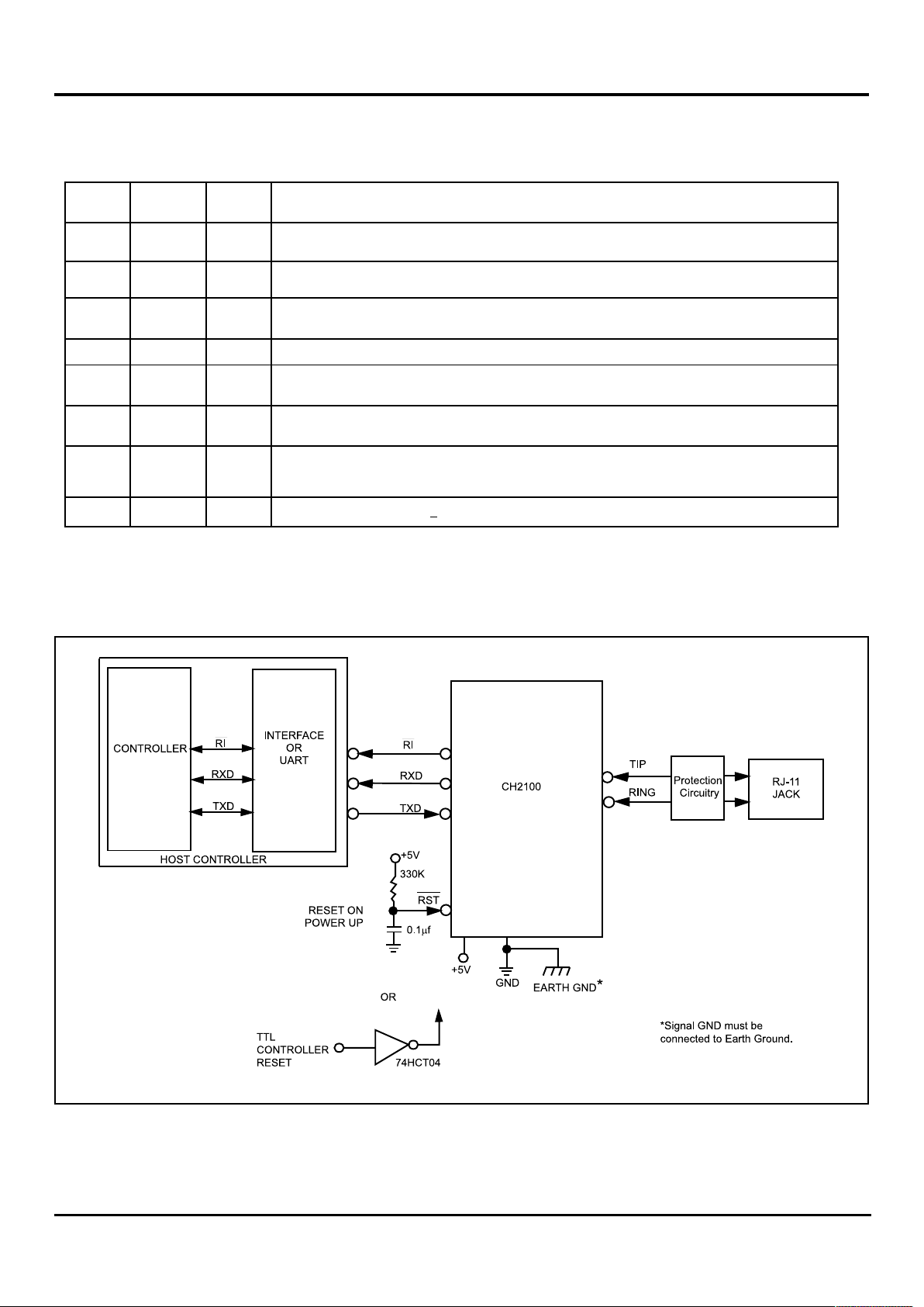
two methods. In the Reset on Power Up method, a resistor/capacitor network is used. Refering to figure 2, the reset pulse, with
the appropriate delays, are generated automatically when 5V are
applied simultaneously to the CH2100 and to the Reset on Power
Up circuit. Delay sending commands to CH2100 for 200ms after
reset has been initiated to allow the CH2100 to properly reconfigure.
TTL Controller Reset.
To reset the modem externally using the second reset method,
TTL Controller Reset, the modem must be powered up and the
5V supply must have stabalized prior to utilizing this method.
Refering to the TTL Controller Reset circuit in figure 2, a 10msec
low-going pulse is sent from the controller through the inverter.
Delay sending commands to CH2100 for 200ms after reset has
been initiated to allow the CH2100 to properly reconfigure.
Cermetek Microelectronics, Inc. Document No. 607-2100 Rev.C (8/99) 31999
Figure 2. CH2100 Application Diagram.
Note: (1) If VCC has a slow power up ramp time, the internal reset may be ineffective.
T able 2. CH2100 Pin Descriptions
NIPEMANEPYTNOITCNUF
1PITO/I
dnapiT.kcajC11-JRdeilppusresuahguorhtdaelpiTs'enilenohpeletehtotstcennocyltceriD
.desreverebyamdnaevitisnesytiraloptoneragniR
2GNIRO/I
dnapiT.kcajC11-JRdeilppusresuahguorhtdaelgniRs'enilenohpeletehtotstcennocyltceriD
.desreverebyamdnaevitisnesytiraloptoneragniR
3
__
IR
O
.NOITACIDNIGNIR siht.gnignirsienilenohpeletlacolehttahtsetacidnisdnoces2rofWOLA
.)sdnoces2rofzH03ro02tuobayllamron(langisgnignirehtfoycneuqerfehtswolloflangis
4DNG-
.DNUORG .kaepotkaepVm05nahtsselebdluohsesioN:etoN
5DXRO
.ATADEVIECER sinoitidnoc1yranibrognikramdevieceR.tuptuoatadevieceRlaireS
.0012HCmorfrellortnoctsohotnoitacinummocrofDXR.HGIHybdetacidni
6DXTI
.ATADTIMSNART dettimsnartsi,noitidnoc1yranibaro,gnikraM.tupniatadtimsnartlaireS
.0012HCotrellortnoctsohmorfnoitacinummocrofDXT.detressasiHGIHanehw
7
_____
TSR
1
I
TESER ehtteserotsm01tsaeltarofWOLdetressaebtsumtupnisihT.WOLevitcA.tupni
,elbaliavasitesermetsysonfI.noitarepolamronrofHGIHdenruternehtsiTESER.medom
.teseraetaercotdnuorgotroticapacfu1.0adnaV5otrotsisermhoK033ahcatta
8CCV-
.YLPPUSREWOP stloV5+
.kaepotkaepVm05nahtsselebdluohsesioN:etoN%5
 Loading...