

CRMET CH1809A, CH1809, CH1804A, CH1804 Datasheet
CH1804/A and CH1809/A
Family of Line Detection and Monitoring Products
Off-Hook Detection. The CH1804A and CH1809A
detector circuits will indicate an Off-Hook condition
when the voltage between the TIP and RING drops
below 20.0VDC. The Off-Hook condition is indicated
by the CH1804A (CH1809A) when the output of OUT1
(OUT2) is >
3.5V.
INTRODUCTION
The CH1804/A and CH1809/A are line status
detectors that are used to monitor line off-hook status
for shared lines, or to detect a severed or cut
telephone line. The CH1804/A is a single line monitor.
The CH1809/A is a dual line device allowing two
telephone lines to be monitored simultaneously and
contains two CH1804/A circuits (See Figure1). For
ease of convertibility, both devices share the same pin
out configuration.
Cut Line Detection. The CH1804 and CH1809
detector circuits will indicate a Cut Line condition when
the voltage between TIP and RING drops below
2.6VDC. The Cut Line condition is indicated by the
CH1804A (CH1809A) when the output of OUT1
(OUT2) is >
3.5V.
The primary application for CH1804 and CH1809
products are security systems where detection of
severed telephone lines is required. In this mode, a
voltage of less than 2.6VDC is detected as a cut line.
An alternate application is collision avoidance in
systems where multiple access to a shared line is
allowed. In this mode, the CH1804A and CH1809A
will indicate when the telephone line voltage drops
below 20VDC thereby detecting an off-hook condition.
FEATURES
• FCC Part 68 approved with conveyed registration.
• Usable on public switched telephone lines and wet
leased lines.
• Detects a severed telephone cable. Does not
require polling.
• Single in line package (SIP) requires minimum PCB
area.
Since the CH1804A/9A products access the PSTN
system, FCC Part 68 approved is required. Cermetek
provides this approval via conveyed registration. A
registration label is supplied for placement on the host
equipment in compliance with FCC Part 68
requirements. The CH1804/A and CH1809/A devices
operate on a single 5-volt supply and provide a
separate active high indication when either of the two
attached lines is cut. The product is contained in a
single in-line package 1.0” long and 0.5” high,
requiring minimal PCB area.
• Low power operation. Single 5V operation.
Table 1. Features Available By Product.
Number of Lines Detection
Feature
CH1804 CH1809 CH1804A CH1809A
Cut Line 1 2
Off-Hook 1 2
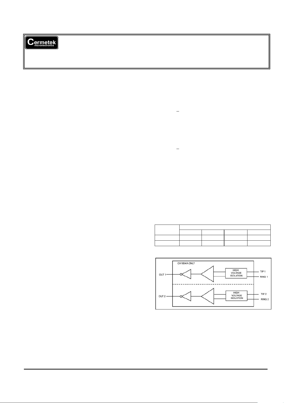
OPERATION
General. Each device contains either one or two
CH1804/A independent line detector circuits. Each
circuit contains separate TIP and RING inputs and
separate active high outputs. A common 5-volt supply
provides power. The output of each detector circuit
has a 45K ohm pull up resistance to 5 volts and a
2.2µF capacitance to ground. This is provided to filter
out zero crossing pulses which can occur during
ringing. Refer to Figure 1.
Figure 1. CH1804/A, CH1809/A Functional Block
Diagram
If the output drive current of the CH1804A/9A is not
sufficient, it is permissible to add a lower value resistor
(this resistor should not be less than 1K ohms)
between the output and 5 volts. However, this will
allow zero crossing pulses to occur. If more drive
current is needed while retaining zero crossing
filtering, an external capacitor must be added to
preserve the original RC time constant. See Figure 2.
ISOLATION REQUIREMENTS
For maximum detection flexibility, incoming telephone
lines should not share a common TIP or RING line. In
addition, the ground of the PSTN system should not be
common to the ground of the system where the
CH1804A/9A is installed. If either of these conditions
2003 Cermetek Microelectronics, Inc. Page 1 Document No. 607-0015 Revision C (05/03)

Cermetek Microelectronics, Inc. CH1804/A and CH1809/A
Potential False Indication. The CH1804/A and
CH1809/A products reside on the telephone line and,
as such, are subject to transients produced by
electrical discharge and ring voltage transitions.
These may cause momentary false Cut Line or OffHook indications. The use of additional external
capacitance on the output may be required to reduce
these false indications. The capacitance value to add
to each output should be determined by appropriate
analysis and testing for the particular application.
Cermetek recommends that the outputs be level
detected as opposed to edge detected to minimize
false indications on excessively noisy lines. Referring
to Figure 2, typical values are 0.1µf and 30K ohms for
CX and RX, respectively.
occur in an installation, the CH1804/9 will only detect
when TIP and RING are both cut. However,
regardless of the installation wiring, the
CH1804A/CH1809A products will always detect an offhook condition. If it is required to detect and identify
which line (i.e., either TIP or RING) has been cut, then
a voltage sense device is required, such as the
Cermetek CH1808 line status detector product.
APPLICATION RECOMENDATIONS
Failure to Detect Cut Line. When using either the
CH1804 or the CH1809 products, external leakage
and capacitance on TIP and RING must be minimized.
Differential leakage to TIP and RING in excess of 0.1
microamperes may appear as a central office battery
voltage thereby causing the CH1804/9 to fail to detect
a cut line. Additionally, Common mode leakage to TIP
and RING in excess of 1 microampere is also
undesirable. Thus, the circuit board layout and
external wiring for TIP and RING must be well
insulated.
SUPPLEMENTAL PROTECTION
If the CH1804A/9A products are being used on
telephone lines that are prone to high voltage
transients, an FCC Part 15 A/B suppressor may be
required. This consists of 1.25 A fuses in both TIP and
RING lines and a 350V voltage suppressor between
TIP and RING for transient protection. A ferrite bead
inductor and 0.1µF capacitor (1500V) to ground may
also be required for EMI/RFI suppression. See
Cermetek Application Note # 126. If the CH1804A/9A
is being used with another Cermetek device where the
supplemental protection is already planned for or
available, the CH1804A/9A can share the protection if
a parallel connection to the TIP and RING pins is
made in front of the protective network.
Off-Hook Indication Delay. Capacitance on TIP and
RING should be minimized as it could retain charge
after a transition and appear as a central office battery
voltage. This will delay detection of an Off-Hook
condition for many tens of seconds. The input
impedance of the detector circuit is approximately 10M
ohms to ground, and the capacitance may have to be
discharged for 3 or 4 time constants to indicate a
detection depending on initial conditions. Thus, it
would be desirable to keep capacitance well below
1µF to keep the delay from exceeding ten seconds.
DESIGN CONSIDERATION FOR FCC
CONFORMANCE
Normal Operation. If the CH1804/A or the CH1809/A
is the only device on the telephone line, leakage and
differential capacitance will tend not to affect normal
operation, since the line capacitance in the central
office or the local loop are minimal. The more devices
that share a given local loop, such as modems and
extension telephones, the greater the capacitance and
leakage possibilities. Sources of capacitance, when
On-Hook, include ring detection circuits in modems.
The CH1804A/9A products include circuits that couple
to the phone line and provide FCC required isolation
and protection. The following guidelines should be
followed to maintain the conveyed FCC Part 68
registration:
1) CH1804A/9A must be mounted away from
hazardous voltages.
2) Connection of the CH1804A/9A devices to PSTN
lines should be made through a standard RJ-11C
jack or another approved connector device.
3) Circuit board traces to the CH1804A/9A TIP and
RING pins must have a spacing of greater than
0.10 inch from all adjacent traces. TIP and RING
traces should have a width of 0.020 inches.
4) TIP and RING traces should be as short as
possible to prevent coupling to other signals lines.
Mount the CH1804A/9A as close to the telephone
line connection as possible.
Figure 2. Application Diagram indicating external
components to increase output drive, decrease
false line cut indications and provide additional
overvoltage protection.
2003 Cermetek Microelectronics, Inc. Page 2 Document No. 607-0015 Revision C (05/03)
 Loading...