

CRMET CH1788-ET, CH1788-3ET, CH1788-3, CH1788 Datasheet
CH1788
Surface Mount PLCC 2400bps Modem
2003 Cermetek Microelectronics, Inc. Page 1 Document No. 607-0018 Revision A2 (07/03)
INTRODUCTION
The CH1788 modem has the smallest footprint and
lowest profile of any commercially available full
function, FCC Part 68 approved 2400bps modem.
Utilizing a 68 pin PLCC form factor and requiring a
minimum amount of PCB space (0.95”x0.95”x
0.255”), the CH1788 affords the design engineer
maximum flexibility. The CH1788 provides two
external interfaces: a CCITT V.24 standard 5 volt
serial interface for routing directly to a UART; and a
TIP and RING interface for connection to the PSTN
telephone line. The CH1788 is compatible with
available industry communication software or may be
controlled with software commands via an embedded
microcontroller.
The CH1788 modem supports asynchronous
operation at 2400bps, 1200bps, and 300bps to both
Bell and CCITT standards. Each device is FCC
approved and Canadian DOT approvable. An FCC
label is supplied. The CH1788 also meets UL 1950
Edition 3 requirements.
The CH1788 family of modems operate from a 5 volt
DC supply (3.3 volt devices are available by special
order). The combination of low power operation, zero
power standby mode and small form factor make the
CH1788 an ideal choice for portable equipment
applications.
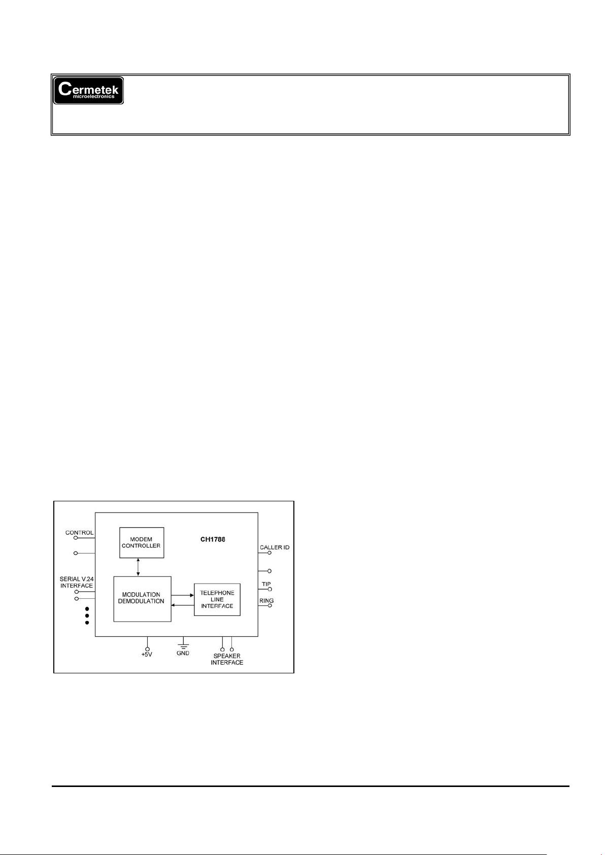
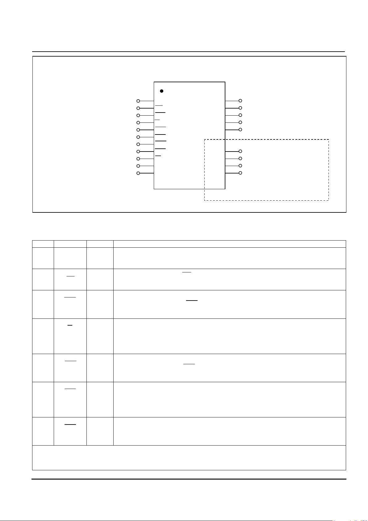
Figure 1. Functional Block Diagram of CH1788.
FEATURES
• Supports data rate standards, CCITT
V.22bis,V.22, Bell 212, and Bell 103, Bell 202,
V.23.
• Fast connect handshaking.
• FCC Part 68 approved and DOT CSA CS-03 Part I
approvable.
• UL 1950 and CSA C22.2 950 Listed.
• AT Command structure.
• Speed buffered operation at: 9600, 2400, 1200
and 300bps.
• Call progress tone detection.
• Caller ID information.
• Line In Use and Priority Pick Up 911 feature
support with external circuitry.
• DTMF generation and detection resident on
CH1788.
• 5 volt operation/ 3.3 volt operation available.
• Low power operation with automatic reduced
power idle and zero power standby modes.
• Low profile PLCC surface mount packaging; fits
standard 68 pin PLCC socket.
• Size: 0.95” x 0.95” x 0.255”(nominal).
CH1788 FAMILY
CH1788 Operating Temperature:
0°C to +70°C
CH1788ET Operating Temperature:
-40°C to +85°C
CH1788-3 3.3 volt Operation
Operating Temperature:
0°C to +70°C
CH1788-3ET 3.3 volt Operation
Operating Temperature:
-40°C to +85°C
DESCRIPTION OF FUNCTIONAL BLOCKS
AND DISCUSSION OF BASIC OPERATIONS
Figure 1 contains a functional block drawing of the
CH1788. The CH1788 is a highly integrated, fullfunction modem, comprised of a modulator/
demodulator, controller, and an FCC Part 68
approved telephone line interface.
Modulation/Demodulation and Modem Controller.
This function is provided by a monolithic modem
integrated circuit. The function is performed to CCITT
standards thereby making the CH1788 compatible
Cermetek Microelectronics, Inc. CH1788 Surface Mount PLCC 2400bps Modem
2003 Cermetek Microelectronics, Inc. Page 2 Document No. 607-0018 Revision A2 (07/03)
with all modems. The ability to execute AT
commands is consistent with industry standards.
Telephone Line Interface or DAA. The CH1788 is
designed to meet 1500VAC RMS isolation and
provide 2122V peak surge protection. Consequently,
the CH1788 satisfies North American and some
international requirements. Note that supplemental
protection is required for FCC Part 68 conveyed
approval (see Figure 3 of this document). This
supplemental protection also improves field reliability
and facilitates FCC part 15 approval.
SUPPORTED FEATURES
AT Command Set. Internal to the CH1788 is an AT
command interpreter. AT commands and their
associated S-registers provide macro functionality.
These commands are summarized in this document
and are detailed in Cermetek publication CH1788 AT
Command and S-Register Reference Guide.
The CH1788 supports command concatenation. A
maximum of 63 characters (excluding AT) may be
included on each command line. S-registers provide
added programmability by allowing key parameters to
be configured for a specific application.
Serial Host Interface. The serial interface is a
standard TTL V.24 5V DC interface. It is functionally
similar to an RS232 interface.
IMPORTANT NOTE
Do not use RS232 interface voltage levels on the
serial pins. Damage may result. Adhere to the TTL
V.24 5V DC interface standard. See Schematic 7
for a suggested circuit to interface RS-232 logic to
the CH1788 TTL V.24 logic.
Command Characters. Each data byte or command
character consists of ten bits: 1 start bit, 1 stop bit,
and eight data bits. The data bits can be either eight
bits with no parity or seven odd or even with 1 parity
bit. The start bit is LOW going. RXD and TXD data is
non-inverted. See the pin descriptions in Table 2.
Data Encoding. The data encoding is user
configurable. The ATB command sets the decoding.
The following CCITT standards are supported:
V.22bis, V.22, Bell 212A, 103, Bell 202 or V.23.
Speed Buffered Mode. Speed Buffering allows the
serial data interface or DTE speed (i.e., the speed
between the host microcontroller and the CH1788) to
be fixed regardless of the connect or DCE speed (i.e.,
the speed between the CH1788 and the remote
modem).
The option exists to disable Speed Buffering by using
the ATY0 command. If Speed Buffering is disabled,
the data connection DCE speed will be equivalent to
the originating modems serial connection DTE speed.
In other words, disabling Speed Buffering forces the
answering modem to connect with a DCE speed
equivalent to the serial DTE speed of the originating
modem.
Data Transmission Speed. The CH1788 allows the
DTE speed to be set to 300, 1200, 2400, or 9600bps.
The DCE speed can be set to 2400, 1200, or 300bps.
A connect message will appear on RXD indicating the
connected data rate.
General Operation. By definition, the originating
modem initiates the PSTN connection and the
answering modem accepts the incoming call. The
connectivity speed (i.e., DCE speed) is determined by
the originating modem.
The originating modem’s DTE speed is established,
in turn, with an initializing AT command issued by the
application’s host controller. Speed Buffering allows
the CH1788 to communicate with the host controller
at a DTE speed that is greater than the connect DCE
speed.
Assuming that the default configuration of the
CH1788 has not been modified with the ATB or ATY0
commands, the answering modem will attempt to
connect to the originating modem at the highest
possible data rate supported by the originating
modem. The connection rate can be less than the
maximum of 2400bps, for example, if the PSTN line is
impaired in some way.
By default upon power up, the CH1788 DTE speed is
set to 9600bps and Speed Buffering is enabled.
Typical Implementation. In a typical
implementation, the CH1788 has a DTE speed of
9600bps and will connect to the remote modem at a
DCE speed of 2400bps. Speed Buffering allows the
CH1788 to negotiate the DCE speed independent of
the DTE speed. Data transfer to the host will be at
the DTE Speed Buffered rate of 9600bps. In this
case, flow control is not required.
It is possible for the DTE speed to be slower than the
DCE speed. For example, a serial interface DTE
speed of 1200 bps and a data rate DCE speed of
2400 bps. In this case, flow control must be
employed by the host to prevent buffer overflow and
lost data.
POWER DOWN
The CH1788 has two power down modes: idle power
standby and zero power standby.
Cermetek Microelectronics, Inc. CH1788 Surface Mount PLCC 2400bps Modem
2003 Cermetek Microelectronics, Inc. Page 3 Document No. 607-0018 Revision A2 (07/03)
Idle Power Standby. In idle power standby mode,
power is switched off automatically by the CH1788
after a period of no activity and is restored
automatically by the CH1788 when activity is again
detected. Activity is defined as a change of status on
DTR, TXD, RST or on any of the other input pins or
an Incoming Ringing signal on TIP/RING. Idle power
mode transitions are transparent to the user.
Zero Power Standby. In applications requiring near
zero power during standby periods, the power may be
switched completely off to the CH1788. This is done
by issuing the AT@Z command or by toggling DTR
after the ATR5 command has been executed.
Normal operation is resumed by performing a 50
msec (minimum) hardware reset on the RST pin.
RING INDICATION
The CH1788 produces a low going 80 msec pulse on
the RI Pin when a valid Incoming Ring signal is
detected. By default, a valid ring signal must fall
within the 10-75 Hz range and have a cadence of 2
seconds on and 4 seconds off. Alternate frequency
ranges and ring cadence’s may be programmed.
CH1788 RESET
The CH1788 may be reset using any of the following
methods. Delay sending commands to the CH1788
for a period of 500 msec after reset has been
completed to allow the CH1788 time to properly
reconfigure.
Hardware Reset. Upon power-up or when power
cycling, the CH1788 will automatically generate an
internal reset pulse. However, if the power supply
comes up too slowly, or has a rise time greater than
50 msec, the internal reset detection circuitry may not
generate the hardware reset.
RST Pin. Initiate a reset externally anytime after the
power supply has stabilized by applying a 50 msec
TTL high reset pulse to the RST pin.
Software Reset. Execute the ATZ command while in
command mode.
DTR Pin. Toggle the DTR pin after executing the
ATR3 command while in command mode.
POWER SUPPLY
Although any standard 5 volt DC supply is
acceptable, the user should be aware that during the
course of normal operation the CH1788 decodes
analog data signals from the PSTN line that are in the
millivolt range. Steps must be taken by the user to
insure that power supply noise on all supply lines,
including ground, does not exceed 50 mV peak to
peak. Any frequency between 20 kHz and 150 kHz
must be less than 500 micro volts peak. If necessary,
use dedicated power and ground planes. Failure to
provide such operating conditions could cause the
CH1788 to malfunction or to function erratically.
Recommendation. To reduce the effects of supply
noise, it is recommended that by-pass capacitors be
placed on the power supply as close to the CH1788’s
supply input (i.e., Pin 20) as practical. A 10 µF
Tantalum capacitor in parallel with a 0.01 µF ceramic
is recommended.
DTMF TONE DETECTION
The CH1788 is capable of detecting DTMF tones
without external hardware.
Setup. Detection will only occur when the CH1788 is
Off-Hook and in the command mode.
DTMF Decoding. The ATJ6 command enables
DTMF decoding. Register S65 will contain the
decoded DTMF result. The S65 register must be
continuously interrogated by the host controller
because the decoded DTMF decimal value is only
present in S65 when the DTMF tones are present on
the PSTN line.
The full range of decoded DTMF decimal values are
listed in Table 1. If the S65 register contains zero, it
indicates that no DTMF tones are present. Note, the
S65 register will contain zero between DTMF tones.
Recommendation. Sample the S65 register at a
rate at least twice (2X) the fastest DTMF tone
periodic rate. DTMF tones typically have a cadence
of 70 msec on and 70 msec off. In this case, the S65
register should be sampled at least every 35 msec.
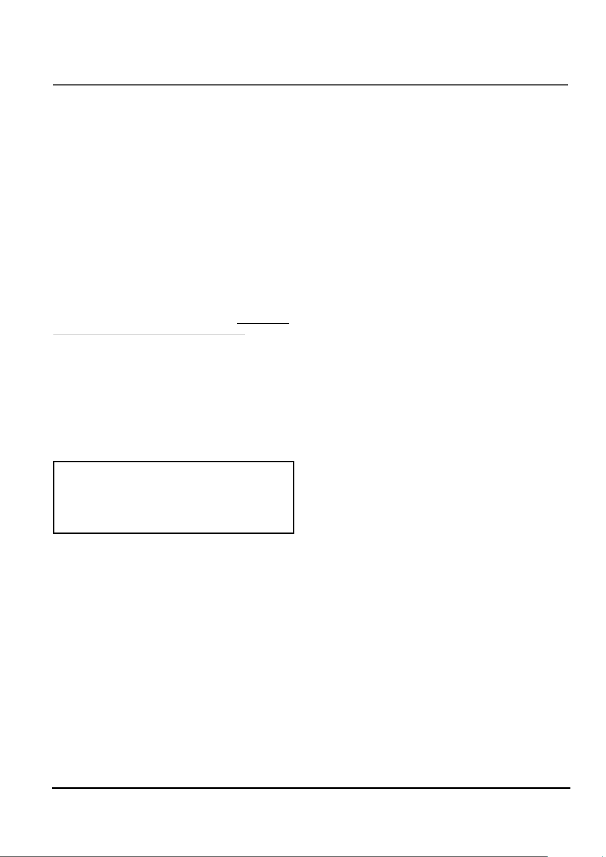
Table 1. DTMF Tone Conversion.
DTMF TONE DECIMAL VALUE
1 129
2 130
3 131
4 132
5 133
6 134
7 135
8 136
9 137
0 138
* 139
# 140
No Tone 0
DTMF TONE GENERATION
The CH1788 is capable of generating DTMF tones
without external hardware. DTMF tone generation is
Cermetek Microelectronics, Inc. CH1788 Surface Mount PLCC 2400bps Modem
2003 Cermetek Microelectronics, Inc. Page 4 Document No. 607-0018 Revision A2 (07/03)
useful for signaling and is supplemental to the DTMF
dialing capability.
Setup. Generation will only occur when the CH1788
is Off-Hook, in the command mode and prior to
carrier generation.
DTMF Encoding. By default, the CH1788 generates
DTMF tones at a 70 msec on/off cycle The cycle can
be modified with register S11.
Issuing an ATDT command string with the desired
DTMF digits and terminating the command string with
a semicolon (;) will cause the CH1788 to immediately
enter command mode after dialing. Alternatively, the
command mode may be entered from the data mode
by issuing the escape sequence (+++) to the
CH1788.
Enter: ATDT1234567890*#;<CR>
Result: Sends the DTMF tones and returns to
command mode. DO not exceed 63
characters on the command line.
DTMF Tones may also be sent using external
circuitry via the voice injection port. See Schematic
2.
CALLER ID
The CH1788 will detect Caller ID (i.e., CID)
information. CID data, when supplied by the local
telephone service provider, is present between the
first and second ring signals. Valid CID data is
preceded by the “CID” designation. This feature is
enabled via register S95.
Setup. CID requires additional external circuitry. An
RC network must be added to the CH1788 V+ and Vpins. See Schematic 4 for details. Register S95
must be set to 8 (the default value) to receive the CID
information. Other caller ID options are available.
See the details of register S95.
Operation. Using the circuit in Schematic 4, monitor
the RI pin for the period between the first and second
ring signal. The decoded CID data will appear on
RXD.
LINE IN USE
The Line In Use (i.e., LIU) feature allows the CH1788
to signal the host when a shared PSTN line is in use.
When in use, the LINE IN USE status message will
appear on RXD and the CH1788 will NOT go OffHook. This feature is enabled via register S110.
Setup. The LIU feature requires additional external
circuitry. See Schematic 5. Additionally, register
S110 must be set to 243.
PARALLEL PICK-UP
The Parallel Pick-Up (i.e., PIU) feature allows the
termination of a CH1788 modem call in progress, and
then allows a standard phone instrument sharing the
same PSTN line to seize the line and obtain a dial
tone. When terminating the modem call, DCD will go
high, if enabled. The PPU-V status message appears
on RXD.
Setup. The Parallel Pick-Up feature requires external
circuitry. See Schematic 6.
Operation. The Parallel Pick-Up circuit detects the
incremental change in Off-Hook voltage on the PSTN
line when a parallel connected phone instrument
goes Off-Hook.
Failure To Detect. The detection circuit in the
CH1788 may not detect the Off-Hook condition for
select phone instruments because these phone
instruments do not change the Off-Hook voltage
sufficiently to allow detection.
There is also the possibility that two devices going
Off-Hook simultaneously may defeat the PPU
detection circuitry.
Recommendation. To avoid a Failure To Detect
condition, use of a prioritized scheme such as that
employed in the 911 Priority Pick-Up application
circuit described below is strongly suggested.
IMPORTANT NOTE
The Parallel Pick-Up feature should only be used in
non-critical applications and never used as a
substitute for the 911 Priority Pick-Up circuit.
911 PRIORITY PICK-UP
The 911 Priority Pick-Up (i.e., 911 PPU) feature
allows the CH1788 to give Off-Hook priority to any
telephone sharing the PSTN line with the CH1788.
Setup. The Parallel Pick-Up feature requires external
circuitry. See Schematic 6.
Operation. If a parallel connected phone instrument
goes Off-Hook while the CH1788 is Off-Hook, the
CH1788 will immediately disconnect to give priority to
the phone instrument.
IMPORTANT NOTE
To ensure that the 911 PPU feature works reliably
in all applications, the CH1788 must be the first
device on the installation’s PSTN line. All other
phone or higher priority instruments must be down
the line from the CH1788.
Cermetek Microelectronics, Inc. CH1788 Surface Mount PLCC 2400bps Modem
2003 Cermetek Microelectronics, Inc. Page 5 Document No. 607-0018 Revision A2 (07/03)
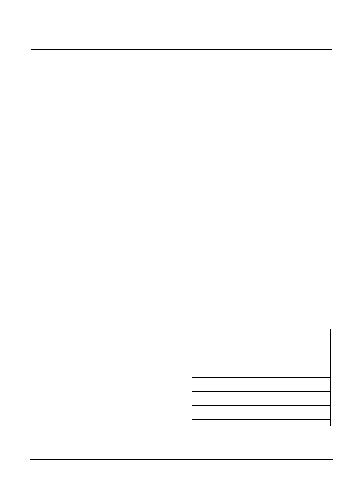
Figure 2. CH1788 Pin Configuration. See Table 2 for detailed Pin Descriptions.
Table 2. CH1788 Pin Descriptions.
PIN NAME TYPE FUNCTION
1
A1
O
Optional Input. Active high. Used when implementing the 911 Priority Pick-Up
circuit or the Line In Use circuit.
2
OH
O
Off-Hook. Active low. OH Indicates when the CH1788 is Off-Hook. Used in Line
In Use, 911 Priority Pick-Up applications and for Audio Control.
3
RTS
I
Request To Send. Active low. Used for optional flow control. Used in conjunction
with the Clear to Send (CTS) pin as a handshaking signal. See the details of
register S90.
4
RI
O
Ring Indication. Active low. For each occurrence of a valid ring signal, this pin will
pulse low for 70 ms. This output signal follows the frequency of the ringing signal
and is typically in the 20 to 40 Hz range with a cadence of 2 seconds on with 4
seconds off.
5
CTS
O
Clear to send. Active low. Used for optional flow control. Used in conjunction with
the Request To Send (RTS) pin as a handshaking signal. See the details of
register S90.
6
DSR
O
Data Set Ready. Active low. A low indicates that handshaking with the remote
modem is in progress and/or the carrier of the remote modem has been detected
and a valid connection is imminent as measured by DCD being active. This feature
is enabled with the N command.
7
DCD
O
Data Carrier Detect. Active low. This output must be enabled with the C
command. When enabled, it will become active when both the originated and
answering modems are connected and a data carrier has been detected.
NOTE: 1. All unused pins should be left unconnected when not required in a specific application,
unless specifically directed otherwise.
2. See DC characteristics before attempting to drive an LED directly from the output of any pin.
Used for LIU/911/Audio Control
CH1788
Top View
A1
OH
RTS
RI
CTS
DSR
DCD
DTR
A2
TXD
RST
RXD
GND
V
CC
S2
S1
V-
V+
TIP
RING
1
2
3
4
5
6
7
8
15
14
13
12
22
21
20
19
9
10
11
18
DTE Signal
Power Input +5V
DTE Si
g
nal
Optional S1/S2 Audio
Monitor/Tone/Voice
V+/V- Optional
CID Input
Telephone Line
Input
Hi
g
h Voltage Section
Used for LIU/911/General IO
DTE Si
g
nal
DTE Si
g
nal
DTE Si
g
nal
DTE Si
g
nal
DTE Si
g
nal
DTE Si
g
nal
Used for LIU/911/Detection
O
p
tional High Reset Input
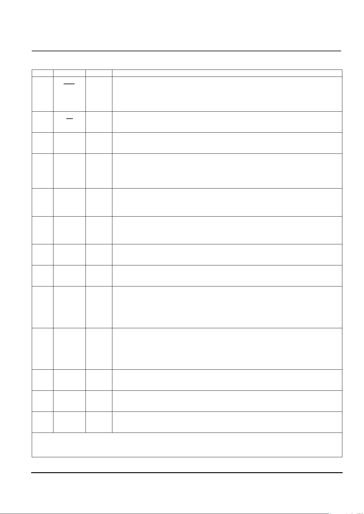
Cermetek Microelectronics, Inc. CH1788 Surface Mount PLCC 2400bps Modem
2003 Cermetek Microelectronics, Inc. Page 6 Document No. 607-0018 Revision A2 (07/03)
Table 2. CH1788 Pin Descriptions (Continued).
PIN NAME TYPE FUNCTION
8
DTR
I
Data Terminal Ready. Active low. The response to this input is controlled by the
Rn command where n specifies the desired options and includes: returning the
modem to the command state, hanging up the modem, resetting the modem, and
placing the modem in zero power mode.
9
A2
I
Optional Input. Active low. Used when implementing the 911 Priority Pick-Up
circuit or the Line In Use circuit.
10
TXD
I
Transmit Data. Serial transmit data input. Data starts with a high to low transition.
Mark or binary 1 condition is indicated by HIGH.
11
RST
I
Reset. Active HIGH. This input must be asserted HIGH for at least 50 ms to reset
the modem. The RST pin must be returned LOW for normal operation to
commence. If a system reset is not available, let this pin float to enable the internal
reset circuitry.
12
RING
I/O
Ring. Telephone connection requires an active public switched telephone line
(PSTN) for normal operation. This line should be routed to the RJ-11C jack through
the recommended protection circuitry.
13
TIP
I/O
TIP. Telephone connection requires an active public switched telephone line
(PSTN) for normal operation. This line should be routed to the RJ-11C jack through
the recommended protection circuitry.
14
V+
I
Caller ID. Used to connect an external RC network to enable caller ID operation.
See the application circuit in the Schematic 4.
15
V-
I
Caller ID. Used to connect an external RC network to enable caller ID operation.
See the application circuit in the Schematic 4.
18
S1
I/O
Audio Port. Optional audio port input. Allows the internal DAA to be shared with
external voice, tone injection or call progress monitoring applications. See the
application circuits in the Schematic 2 and 3. Note that the CH1788 is FCC
approved for data applications only. Inclusion of voice or other audio functions may
require additional certification by the FCC.
19
S2
I/O
Audio Port. Optional audio port input. Allows the internal DAA to be shared with
external voice, tone injection or call progress monitoring applications. See the
application circuits in the Schematic 2 and 3. Note that the CH1788 is FCC
approved for data applications only. Inclusion of voice or other audio functions may
require additional certification by the FCC.
20
V
CC
--
Power Supply. 5 Volt DC +/- 5%. Supply noise should be less than 50 mV
pp
. Also
available at for 3.3 volt DC operation, upon special request.
21
GND
-
Ground. Circuit ground. Use recommended bypass capacitors between GND and
VCC.
22
RXD
O
Receive Data. Serial receive data output. Data starts with a high to low transition.
Received mark or binary 1 condition is indicated by HIGH.
NOTE: 1. All unused pins should be left unconnected when not required in a specific application,
unless specifically directed otherwise.
2. See DC characteristics before attempting to drive an LED directly from the output of any pin.
Cermetek Microelectronics, Inc. CH1788 Surface Mount PLCC 2400bps Modem
2003 Cermetek Microelectronics, Inc. Page 7 Document No. 607-0018 Revision A2 (07/03)
CALL PROGRESS MONITORING
Call Progress Monitoring allows a call to be monitored
during the dialing sequence. This feature becomes
active when the CH1788 goes Off-Hook and
automatically disables when DCD is detected. It is
also inactive if a connection attempt should fail and
the CH1788 goes back On-Hook. To enable this
feature, the DCD line must be activated with the
ATC1 command.
Setup. This feature requires additional external
circuitry. See Schematic 2. Although the circuit in
Schematic 2 uses a variable resistor to adjust the
speaker volume, a fixed value resistor may be
substituted.
Alternate Setup. Control of the speaker can
alternately be performed under command control. To
implement this alternate control method, modify the
circuit in Schematic 2 by connecting resistor R5 to A1
instead of DCD. This allows register S101 to be used
to turn the speaker on or off. Set S101 to 1 to turn
the circuit on, set S101 to 0 to turn the circuit off.
FAST CONNECT HANDSHAKING
The CH1788 supports a fast handshaking (often
called “quick connect”) feature. This feature is
controlled via the L3 command.
Typically, the initial handshaking sequence takes
between 10 and 20 seconds to complete. When fast
handshaking is selected, the handshaking sequence
will take between 4-8 seconds. Fast Connect
Handshaking will work with any compatible modem.
LONG SPACE DISCONNECT
The long space disconnect signal is used to force the
CH1788 to release the PSTN line and go back OnHook.
Setup. To enable this feature, bit 7 of register S110
most be set to 1. See the details of register S110.
VOICE INJECTION
It is possible to share the CH1788’s internal DAA with
external applications. This allows one PSTN line to
be shared between an external voice application and
the CH1788 modem. This feature is controlled via
register S101.
Setup. This feature requires additional external
circuitry. See Schematic 3. This application
implements Voice Injection via the S1 and S2 pins
and requires a two to four wire converter and a relay
circuit. Set S101 to 1 to activate Voice Inject and set
S101 to 0 to deactivate Voice Inject.
Operation. The two to four wire converter circuit
provides for simultaneous voice in and voice out (with
respect to ground). This circuit must be capacitor
coupled (i.e., C7) to the CH1788 and isolated from
ground (i.e., C6). Voice/data switching is controlled
by setting register S101 appropriately.
During Voice Injection, the voice signal must not
exceed 2.187 V
pp
(i.e., zero dB) per FCC maximum
permissible limits. When sending data, the voice
circuit must be fully disconnected from the line (i.e.,
Voice Inject deactivated) or data corruption will occur.
IMPORTANT NOTE
When utilizing the Voice Injection circuit, it is
necessary to submit the end product containing the
CH1788 Voice Injection feature to an FCC approved
testing facility for re-approval of the end product per
FCC Part 68 requirements.
MODEM CONTROL
The CH1788 may be controlled with ASCII AT
commands sequences. The commands are sent to
the CH1788 serially via the TXD pin. After execution
of a received command string, the CH1788 returns a
serial status message on RXD.
INITIALIZING THE MODEM
The CH1788 must be initialized before the CH1788
will recognize commands. Initialization is a two step
activity consisting of:
1. Hard Reset. This is accomplished by applying a
hardware reset pulse to pin RST for 50 ms. The
internal reset may be used by cycling the power.
The modem should not be accessed for 500
msec after a reset has occurred.
IMPORTANT NOTE
Delay the sending commands to the CH1788 for a
period of 500 msec after reset has been completed
to allow the CH1788 time to properly reconfigure.
2. Initial CH1788 Training. This will establish the
word bit length and type for communication with
the host. The word size should not be more than
10 bits including start and stop bits and is typically:
1 start bit, 1 stop bit, 8 data bits and with no parity.
The CH1788 is trained by the host with the
AT<CR>. The serial data rate (i.e., the DTE
speed) at which the host sends the AT<CR>
command initializes the modem DTE Speed.
3. The CH1788 S registers must be re-configured to
their required settings after a soft reset, hardware
reset, or power loss.

Cermetek Microelectronics, Inc. CH1788 Surface Mount PLCC 2400bps Modem
2003 Cermetek Microelectronics, Inc. Page 8 Document No. 607-0018 Revision A2 (07/03)
4. Cermetek recommends issuing the following setup
string ATS13=39S73=176<CR> for best
performance.
THE COMMAND FORMAT
Typical commands consist of three elements: the
attention sequence, the commands themselves, and
a terminating carriage return.
AT[commands]<CR>.
Where: AT represents attention sequence.
[Commands] represents command strings.
<CR> represents carriage return (ASCII 13
or HEX 0D).
Training the Modem. The CH1788 must be trained
to set the DTE speed (i.e., to match its host’s speed
and parity) so that the CH1788 is able to recognize
serial asynchronous commands sent to it by the
host’s UART. The host must retrain the CH1788
each time a reset is performed.
Modem Training Command Sequence. The
CH1788 is trained by sending it the AT sequence:
Enter: AT<CR>
Result: OK
Where: A and T may be either upper or lower case
but must be the same case.
<CR> represents carriage return
The AT sequence is referred to as the attention
sequence. When received, the CH1788 will respond
with one of the following status messages, depending
on whether the CH1788 is optioned for Terse
(abbreviated) or Verbose (English) status messages.
Result: 0<CR> (Terse)
or
Result: <CR><LF>OK<CR><LF> (Verbose)
Where: <CR> represents carriage return (ASCII 13
or HEX 0D).
<LF> represents line feed (ASCII 10 or
HEX 0A).
After responding, the CH1788 will be in command
mode and ready to accept additional commands. An
alternate attention sequence A/ may be sent. This
command causes the previously entered command
string specified with the AT prefix to be executed.
AT Command Set. The available commands are
summarized in Table 5. Note that each command
may have several options and the options may be
influenced by various S-Register values. It is
recommended that the designer review Cermetek
publication CH1788 AT Commands and S-Registers
Reference Guide.
AT Command Structure. When issuing commands
to the CH1788, the backspace character-control-H
(ASCII 8 or HEX 08) may be used to perform
character editing.
Multiple commands may be placed on the command
line as long as the command line does not exceed 63
characters, excluding the letters AT. By way of
example, the command string below instructs the
CH1788 to configure itself to suppress character
echoing when in command mode E0 and then put
itself in the answer state A.
Enter: ATE0A<CR>
Result: OK
MODEM STATES
The CH1788 is in either of two states: command
mode or data mode. The CH1788 will only respond
to AT commands when it is in command mode.
When the modem is idle, by default it is in command
mode.
When data transmission is in progress, the CH1788 is
in data mode and will not recognize/respond to AT
commands. To cause the CH1788 to recognize
commands when in data mode, the host must send
an escape sequence to the CH1788 forcing the
CH1788 out of data mode and into command mode.
Only then will the CH1788 respond to AT commands.
If the CH1788 is Off-Hook, connected to a remote
modem and placed in command mode by its host, the
CH1788 will not transmit any commands received
from its host to the remote modem. However, when
in this state, the CH1788 will not receive data from
the remote modem.
Result Codes. After execution of an AT command
and at the completion of each dial attempt, the
CH1788 will deliver a status message on RXD.
Referring to Table 3, the message can be a Terse
(numeric) or Verbose (English) message. The
message type is controlled via the V command.
Various combinations of the listed result codes can
be selected with the W and X commands.
Escape Sequence. The escape sequence consists
of a “guard time” of one second (a period where no
characters are sent to the modem), followed by 3
escape characters (typically +++), followed by
another guard time of one second. The escape
character code is set in register S2. by default, the
escape character is set as “+.” There is no required
delay between characters. When the escape
sequence has successfully been sent, the escape
characters will not be transmitted to the remote
modem.
 Loading...