

CRMET CH1782A Datasheet
CH1782A
Family of Ultra Small Modem Modules V.22bis-2400bps
INTRODUCTION FEATURES
The CH1782A Ultra Small Modem Module is a pin
compatible and functional replacement for the
CH1782. The CH1782A replaces the CH1782 due to
the obsolescence of the modem chip set in the
CH1782 by the manufacturer. The CH1782A is
recommended as a replacement for the CH1782, but
not for new designs. The CH1782A is a small, full
function 2400bps modem component that is FCC Part
68 approved. It offers a fast and easy way to integrate
a modem into an OEM product while utilizing a
minimum amount of PCB space and having only an
0.50” height. The modem component has two
interfaces, a CCITT V.24 serial interface that can be
routed directly to a UART and a Tip and Ring signal
which goes directly to an RJ-11 jack for telephone line
connection. The modem can be controlled with
industry standard AT commands and, hence, is
compatible with available industry communication
software.
• Supports Standards CCITT V.22bis, V.22, Bell
212, and Bell 103
• FCC Part 68 approved and DOC approvable
• AT Command structure – with extensions
• 1000 VAC isolation barrier
• Single 5 volt operation
• Low power operation with automatic reduced
power standby mode
• Automatic adaptive and fixed compromise
equalization
• Size: 1.0”X1.25”X0.53”
The CH1782A supports asynchronous operations at
2400bps, 1200bps, and 300bps to Bell and CCITT
standards.
The resident telephone line interface, or Data Access
Arrangement (DAA), while being FCC approved, is
also Canadian DOC approvable and can be approved
in other countries that require 1000 VAC isolation.
The CH1782A operates off a regulated single 5-volt
supply. The low power operation and automatic
standby mode male it ideal for portable equipment,
which is further enhanced by its small size.
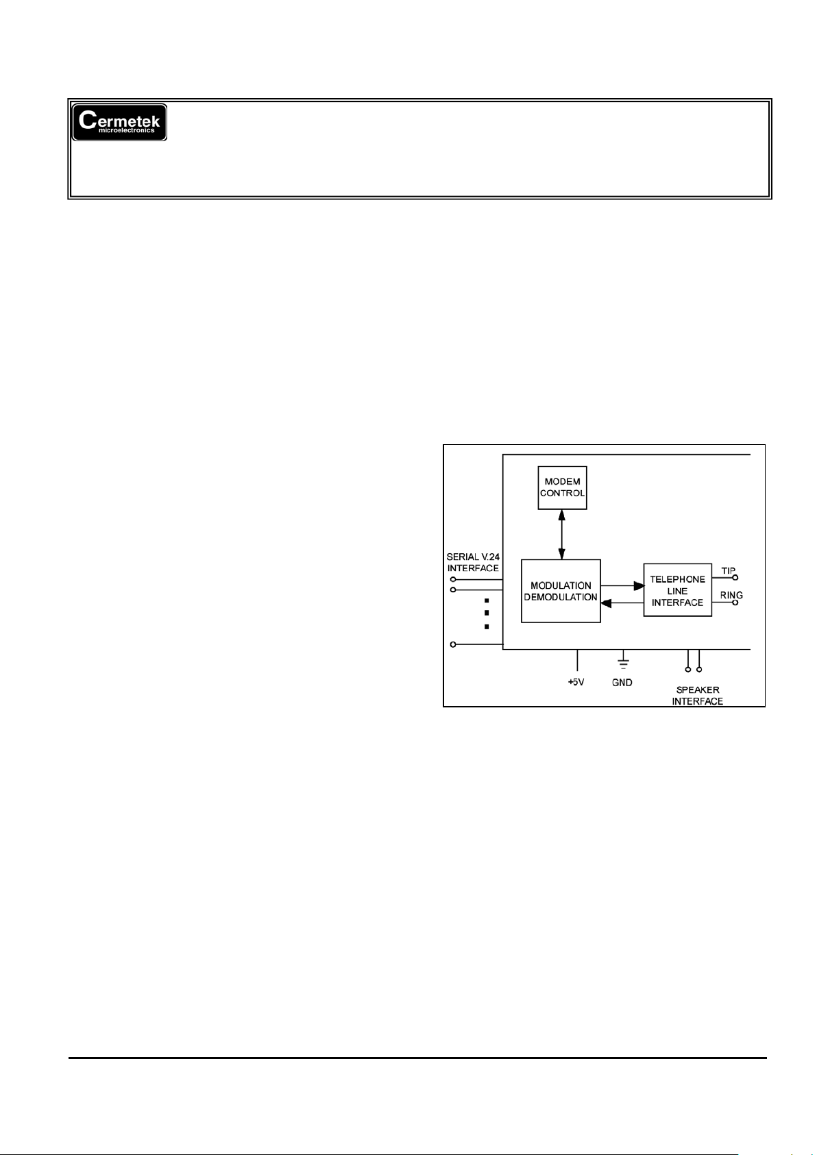
Figure 1. CH1782A Functional Block Diagram.
Telephone Line Interface or DAA. The CH1782A is
designed to meet North American telephone standards
as set by FCC Part 68 and DOC. The telephone line
interface is designed to meet 1000 VAC and 1500 volt
peak surge isolation, among other parameters. As
such, it will meet U.S. and Canadian requirements, as
well as other international requirements that specify
that level of isolation. Cermetek manufacturers other
modules that meet more stringent international
requirements.
DESCRIPTION OF FUNCTIONAL BLOCKS
AND DISCUSSION OF BASIC OPERATIONS
Figure 1 is a functional block drawing of the CH1782A.
The CH1782A is a highly integrated, full-function
modem, comprised of a modulator/demodulator,
controller, and a FCC Part 68 approved telephone
PSTN line interface.
Modulation/Demodulation and Modem Controller.
These functions are provided by a monolithic modem
integrated circuit. This IC has built-in facilities to
accommodate integrated AT command control and
contains the necessary resident interfaces for general
communication and routing to the DAA.
The CH1782A is pre-approved to FCC Part 68; and is
shipped from the factory with a label that indicates the
registration number and ringer equivalent affixed to the
unit. An additional label is provided that should be
prominently displayed on the outer system enclosure.
As with most countries, except the U.S., Canada
requires submission of the product containing the
CH1782A for DOC approval. This can be done by
2002 Cermetek Microelectronics, Inc. Page 1 Document No. 607-0009 Revision C (01/03)
Cermetek Microelectronics, Inc. CH1782A Family of Ultra Small Modem Modules V.22bis-2400bps
submitting the design to a test house or consultant.
Call Cermetek for assistance.
to activate a relay which can switch a telephone on or
off the Tip and Ring incoming PSTN lines. This
feature allows any telephone associated with the
CH1782A to be disconnected when a data call is in
progress, thereby preventing the data from being
disturbed by an inadvertent telephone pick-up. See
Figure 2.
SUPPORT FEATURES
AT Command Set. A 40-character command line is
supported. The command line starts with AT and
may contain standard or enhanced commands. The
commands are compatible with EIA Document
TR302.2/88-08006.
Speed and Parity Selection. Prior to call initiation,
the host controller trains the modem to the host
speed (2400,1200 or 300bps) and parity (odd, even,
mark, space, or none) via a host-initiated training
sequence. This training also sets the speed of the
data for originate calls. The CH1782A will
automatically adjust to the originator’s speed when
answering calls.
Serial Host Interface. The serial interface is a V.24
(EIA-232) compatible interface. Ten Bits total: 1 start
bit, 1 stop bit, and eight data bits which can be either
eight bits with no parity or seven odd or even with
parity. The start bit is LOW going. RXD and TXD
data is non-inverted. See pin description in Table 2.
The CH1782A matches the host’s parity when it
returns status messages to the host. During a data
connection, however, the modem passes parity
through without interpretation or alteration.
Speaker Interface. The SPK output reflects the
receiver analog input and provides a signal that can
be used to monitor call progress. The SPK signal can
drive a 300 Ω load directly. Typically, the SPK signal
is input into an audio power amplifier and the
amplifier, in turn, drives the speaker coil. The
speaker is activated with the ATMn command. The
speaker volume is adjusted using the ATLn
command, where n is 0,1,2,or 3. Increasing numbers
correspond to higher volume. Figure 5 indicates one
method of driving an external 8 Ω speaker.
Sleep Mode. To minimize power consumption, the
CH1782A includes a power down feature called
Sleep Mode. When activated, the CH1782A will
automatically enter Sleep Mode after 0 to 254
seconds of inactivity. The inactivity delay is selected
using the ATS24 command. The CH1782A is
delivered from the factory with a 5 second inactivity
delay enabled (i.e., ATS24=5). The CH1782A
returns to normal operation when a ring signal is
received or upon an input low signal on the TXD pin.
ATS24=255 disables the Sleep Mode and is the
default if no value is set in register S24.
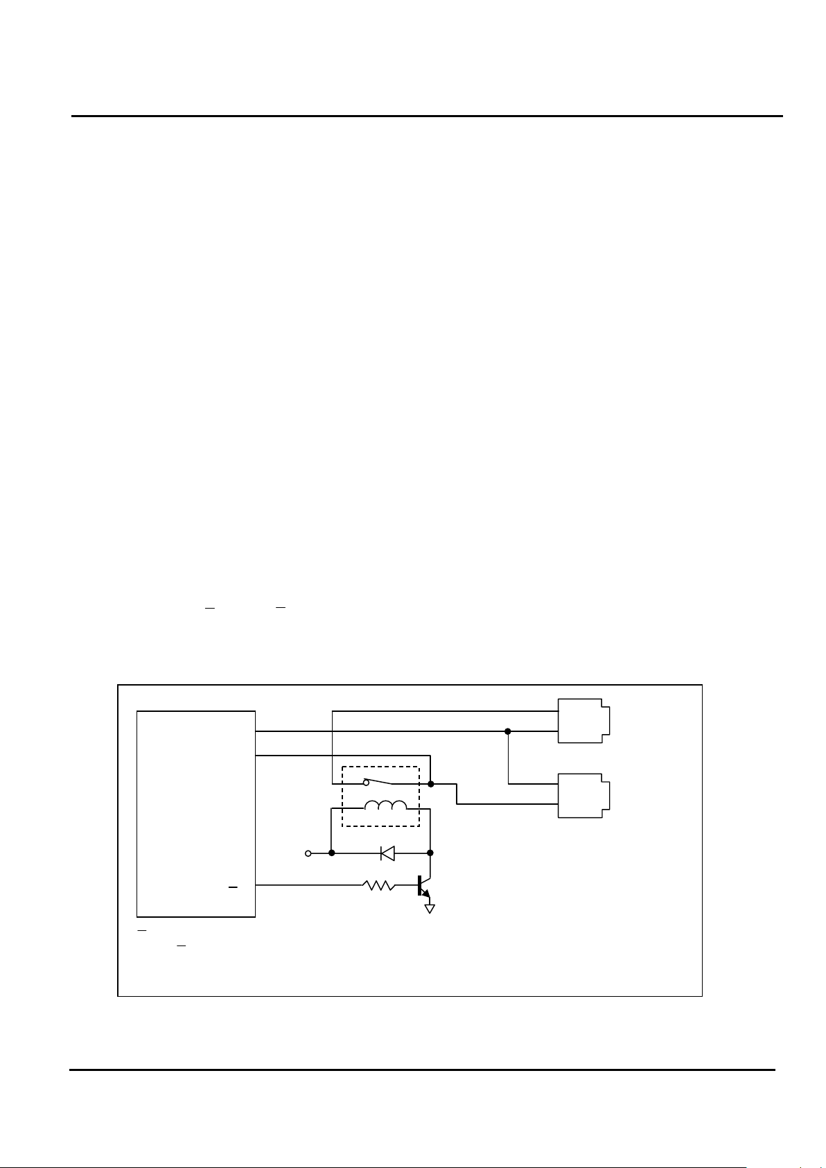
Phone Control. Cermetek ’s CH1782A contains a pin
called Voice or Data (V/D). The V/D pin toggles high
when the modem goes off hook. This pin can be used
V/D pin is used to create a separate port for telephone connection sharing of the tip and ring
lines. V/D is TTL compatible (IOL = 1.6mA, VOL = 0.4V) and is active during data connection
thereby isolating the telephone from the tip and ring lines. (Note: the relay chosen must meet
the appropriate regulatory agency requirements).
V/D
TELEPHONE
LINE
OPTIONAL
PHONE
RJ-11
Jack
RJ-11
Jack
TIP
TIP
RING
RING
+5V
IN914
10K
1
2
12
CH1782A
Figure 2. Use of V/D pin to ensure that a shared PSTN line does not inadvertently disturb
an active data call.
2002 Cermetek Microelectronics, Inc. Page 2 Document No. 607-0009 Revision C (01/03)

Cermetek Microelectronics, Inc. CH1782A Family of Ultra Small Modem Modules V.22bis-2400bps
A SLEEP output signal is available to control power to
external devices. In Figure 6, a FET controlled by the
SLEEP signal turns of the external speaker amplifier
when the CH1782A enters Sleep Mode. In Sleep
Mode, power is reduced to approximately 50% of
normal operating power.
NOTE
A 2400-baud connection rate will only result if both
modems are initially set at 2400 baud.
Table 1. Connection Rates.
Answering
Modem Initial
Trained Rate
Connection Rate Resulting
When Calling Modem Initial
Rate Is:
300 1200 2400
300 300 1200 1200
1200 300 1200 1200
2400 300 1200 2400
Guard Tone. A guard tone of 550 Hz or 1800 Hz can
be generated at 6 dB or 9 dB below the transmit level,
respectively, by using the &Gn command. Refer to
“Cermetek AT Commands and S-Registers reference
Guide” or the Cermetek web site at
http://www.cermetek.com
.
Ring Indicator (RI). The RI pin follows the frequency
of the ring signal and toggles low when the CH1782A
detects an incoming call. The ring signal is typically
20 to 30 Hz and is on for 2 seconds and off for 4
seconds. Although not TTL compliant, the RI pin can,
nonetheless, be utilized to activate external circuitry
including the external RST pin.
Answer Tone. A CCITT (2100 Hz) or Bell (2225Hz)
answer tone is generated depending on the selected
configuration. Refer to “Cermetek AT commands and
S-Registers Reference Guide” or the Cermetek web
site at http://www.cermetek.com
.
Data Encoding. The data encoding conforms to
CCITT recommendations V.22bis or V.22, or
Bell212A, or 103, depending on the selected
configuration. Refer to “Cermetek AT commands and
S-Register Reference Guide” or the Cermetek web
site at http://www.cermetek.com
.
When using the RI pin, it is recommended that a
Schmitt Trigger or the Isolated Envelope Detect
Circuit in Figures 3 or 5 be placed between the RI pin
and the external load.
Power Supply. The CH1782A modem module is a
complex set of sub-systems. During the course of
normal operation the CH1782A decodes analog
signals from the telephone line that are in the millivolt
range. Steps must be taken by the user to guarantee
that power supply noise on all supply lines, including
ground, does not exceed 50 mV peak to peak. Any
frequency between 20 kHz and 150 kHz must be less
than 500 micro volts peak. If necessary, use
dedicated power and ground planes. Failure to
provide such operating conditions could cause the
CH1782A to malfunction or to function erratically.
Line Equalization. Transmitter and receiver digital
filters compensate for delay and amplitude distortion
during operation on nominal phone lines. In addition,
automatic adaptive equalization in the receiver
minimizes the effects of inter symbol interference.
Transmission Speed. In normal operation, the
originating modem initiates the call and attempts to
connect to the answering modem at a speed
established by the originating modem’s controller prior
to call initiation. This is referred to as the Initial
Trained Rate. Upon receiving the call, the answering
modem will attempt to connect to the originating
modem at its Initial Trained Rate. If these two rates
are identical, the connection is made. If the speeds
differ, the answering modem must adjust its rate or
terminate the call. Table 1 indicates the connection
rate that will result when the calling modem’s Initial
Trained Rate and the answering modem’s Initial
Trained Rate are different.
The CH1782A requires a single +5V ±5% supply. It
is recommended that by-pass capacitors be placed
on the power supply as close to the modem’s supply
input as practical. It’s recommended a 10 µF
Tantalum capacitor in parallel with a 0.01 µF ceramic
capacitor be used.
INITIALIZING THE MODEM
MODEM CONTROL
Before commands may be sent to the CH1782A, the
CH1782A must be initialized. Initialization is a two
step activity consisting of:
The CH1782A modem may be controlled by sending
serial ASCII command sequences. The commands are
sent to the modem serially on TXD. After execution of
the command, the modem returns a serial status
message on RXD, to indicate the completion status of
the command.
1. Hard Reset. This is accomplished by applying a
hardware reset pulse to pin RST or by switching
the power off and then back on.
2002 Cermetek Microelectronics, Inc. Page 3 Document No. 607-0009 Revision C (01/03)
2. Initial modem training. The CH1782A must be
trained to the host’s speed (2400, 1200, 300bps)
and parity (odd, even, mark, space or none).

Cermetek Microelectronics, Inc. CH1782A Family of Ultra Small Modem Modules V.22bis-2400bps
[Commands] represents command strings.
These activities are briefly described below.
<CR> represents carriage return (ASCII 13
or HEX 0D).
Reset. Upon applying power to the CH1782A, the
CH1782A automatically generates an internal reset
pulse. The user may also reset the modem externally
by applying a high-going reset pulse to the RST pin
for at least 10ms after the +5V power supply has
stabilized. Delay sending commands to CH1782A for
200ms after reset has been initiated to allow the
CH1782A time to properly reconfigure.
When entering commands to the modem, the
backspace character-control-H (ASCII 8 or HEX 08)
may be used to edit mistakes. AT and A/ may not be
edited. Multiple commands may be placed in the
command line. A command line may be as long as
40 characters, excluding the letters AT. By way of
example, the command below instructs the CH1782A
to configure itself to not echo characters when in
command mode E0 and then put itself in answer
mode A.
Training the Modem. Each modem must be trained
to match its host’s speed and parity so that it is able
to recognize serial asynchronous commands sent to it
by the host’s is UART. The host must retrain the
modem each time a reset pulse is applied on RST or
after a RESET serial command has been issued.
Enter: ATE0A<CR>
Result: OK
Modem Training Command Sequence. The
CH1782A is trained by sending it the following
sequence:
AT Command Set. The available command set is
divided into four types of commands: dial modifiers,
basic commands, ampersand and percent
commands. Refer to the complete list in Table 5.
Enter: AT<CR>
Result: OK
AT Command Data Rate. With the serial interface,
the rate is speed sensed for parity and format.
Where: A and T may be either upper or lower case
but must be the same case.
<CR> represents carriage return
THE STATUS MESSAGES
The AT sequence is referred to as an attention
sequence. The CH1782A will respond with one of the
following status messages, depending on whether it
is optioned for Terse (abbreviated) or Verbose
(English) status messages.
The CH1782A responds with a status message after
each command is executed. This status message
may either be a single digit followed by a carriage
return or a carriage return and line feed with a
message in English, followed by a carriage return and
line feed.
Result: 0<CR> (Terse)
or
n command. Where n=0, 1, 2, 3, 4 establishes the
result codes allowed by the user.
Result: <CR><LF>OK<CR><LF> (Verbose)
Where: <CR> represents carriage return (ASCII 13 or
HEX 0D).
X0: Result Codes 0, 1, 2, 3, 4 allowed
<LF> represents line feed (ASCII 10 or HEX
0A).
X1: Result Codes 0, 1, 2, 3, 4, 5, 10 allowed
X2: Result Codes 0,1, 2, 3, 4, 5, 6, 10 allowed
X3: Result Codes 0, 1, 2, 3, 4, 5, 7, 10 allowed
After responding with an OK, the CH1782A is in idle
mode and is ready to accept additional commands.
An alternate attention sequence A/ may be sent
which behaves much like the AT sequence except
that it causes the previously entered command
specified with an AT prefix to be executed. When
given, both the AT and A/ must be in upper case
ASCII. No carriage return is needed for the A/
command.
X4: Result Codes 0, 1, 2, 3, 4, 5, 6, 7, 10 allowed.
NOTE
The CH1782A is factory set to X4, which allows all
result codes.
MODEM STATES
The CH1782A can be in either command mode or
data mode. When the modem is idle, it is in
command mode by default and will recognize
commands. When data transmission is in progress,
the CH1782A is in the data mode state and will not
recognize commands. To force the CH1782A to
recognize commands, the host must send an escape
sequence to the CH1782A forcing it out of data mode
and into command mode.
THE COMMAND FORMAT
Typical commands consist of three elements: the
attention sequence, the commands themselves, and
a terminating carriage return.
AT[commands]<CR>.
2002 Cermetek Microelectronics, Inc. Page 4 Document No. 607-0009 Revision C (01/03)
Where: AT represents attention sequence.
Cermetek Microelectronics, Inc. CH1782A Family of Ultra Small Modem Modules V.22bis-2400bps
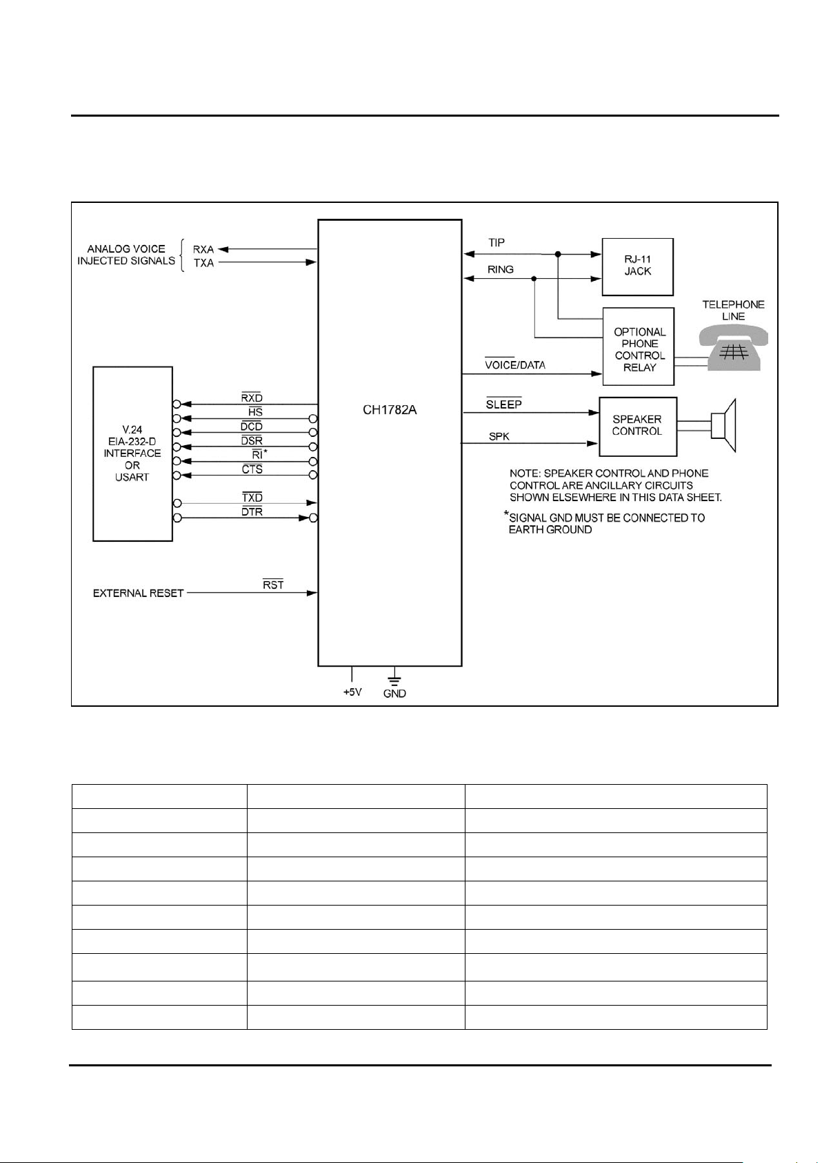
Figure 3A. CH1782A Application Diagram indicating the use of Voice/Data pin to control an optional
telephone relay for a secondary telephone.
Table 2. Summary of Result Codes and Meanings.
Result Codes Status Message Meaning
0 OK Command Executed
1 CONNECT Carrier detected at 300bps
2 RING Ring Detected
3 NO CARRIER Did not detect carrier
4 ERROR Entry error
5 CONNECT 1200 Carrier detected at 1200bps
6 NO DIAL TONE Off-hook, but no response after 5 seconds
7 BUSY Busy signal detected
10 CONNECT 2400 Carrier detected at 2400bps
2002 Cermetek Microelectronics, Inc. Page 5 Document No. 607-0009 Revision C (01/03)
Cermetek Microelectronics, Inc. CH1782A Family of Ultra Small Modem Modules V.22bis-2400bps
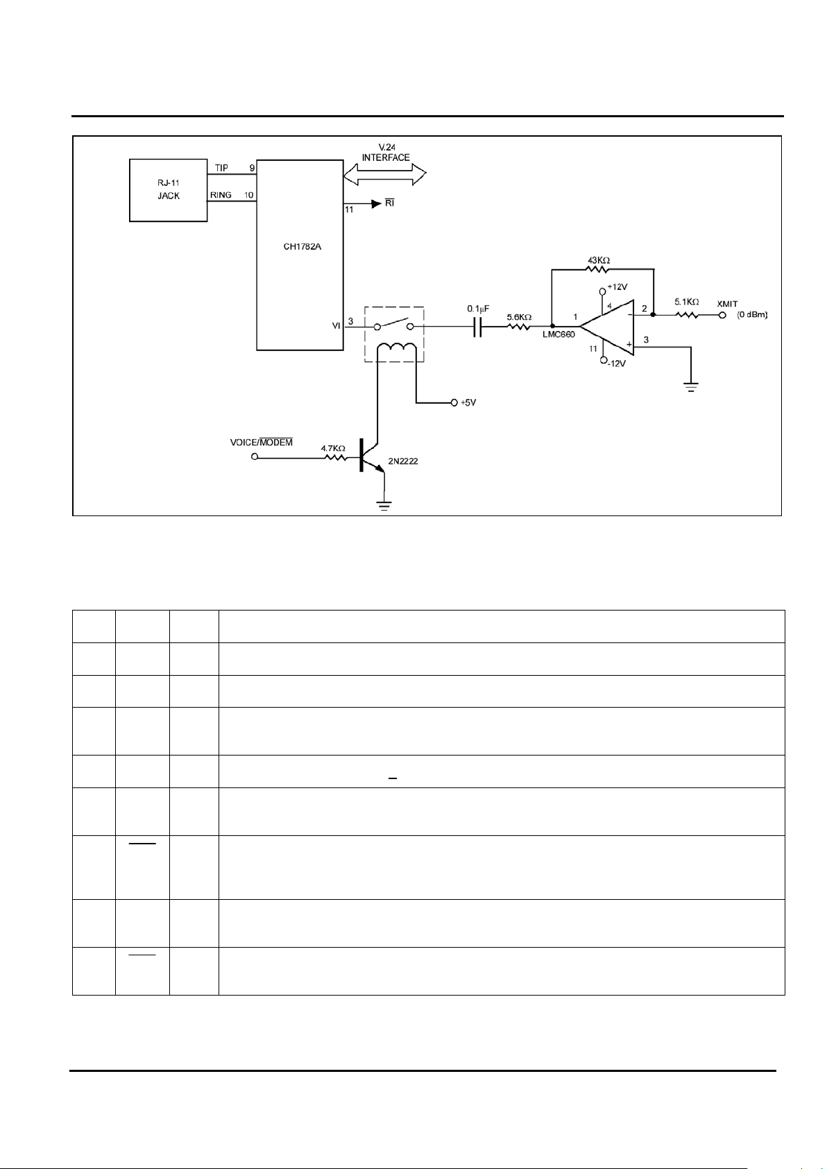
Figure 3B. CH1782A Voice Application illustrating the use of the VI pin to control external injection of voice
or data into the CH1782A and onto the PSTN line.
Table 3. CH1782A Pin Description.
PIN NAME I/O FUNCTION
1 - NC NO CONNECTION. Formerly RTS – Not supported by the CH1782A.
2 GND - GROUND. Note: Noise should be less than 50mV peak to peak.
3 VI I/O VOICE INJECTION. Use this port to transmit/receive voice or DTMF signals to/from the
PSTN Line.
4 VCC - POWER SUPPLY. 5 volts + 5% Note: Noise should be less than 50mV peak to peak.
5 RXD O RECEIVE DATA. Serial Receive data output. Received marking or binary 1 condition is
indicated by HIGH.
6 DTR I DATA TERMINAL READY. Active LOW. Switching off DTR can either return modem to
command state, disconnect phone call, or reset modem. DTR should be set LOW when not
used.
7 DSR O DATA SET READY. LOW indicates handshaking with a remote modem is in progress, and/
or the data carrier of a remote modem has been detected.
8 DCD O DATA CARRIER DETECT. LOW indicates a data carrier from a remote modem is detected.
Must be enabled using the &C1 command.
2002 Cermetek Microelectronics, Inc. Page 6 Document No. 607-0009 Revision C (01/03)
 Loading...