


Critikon Dinamap IR Modul Service Manual
INVASIVE PRESSURE MODULE
INTRODUCTION
This area contains service information about the
Model 7330 Invasive Pressure (IP) Module. The
Module can monitor two channels of invasive
pressure derived from resistive bridge pressure
transducers. Monitored blood pressure typically
includes pulmonary artery pressure or central
venous pressure. Heart rate values are also
determined by a weighted average formula that is
applied to pulse rate data obtained from a pulsatile
invasive pressure.
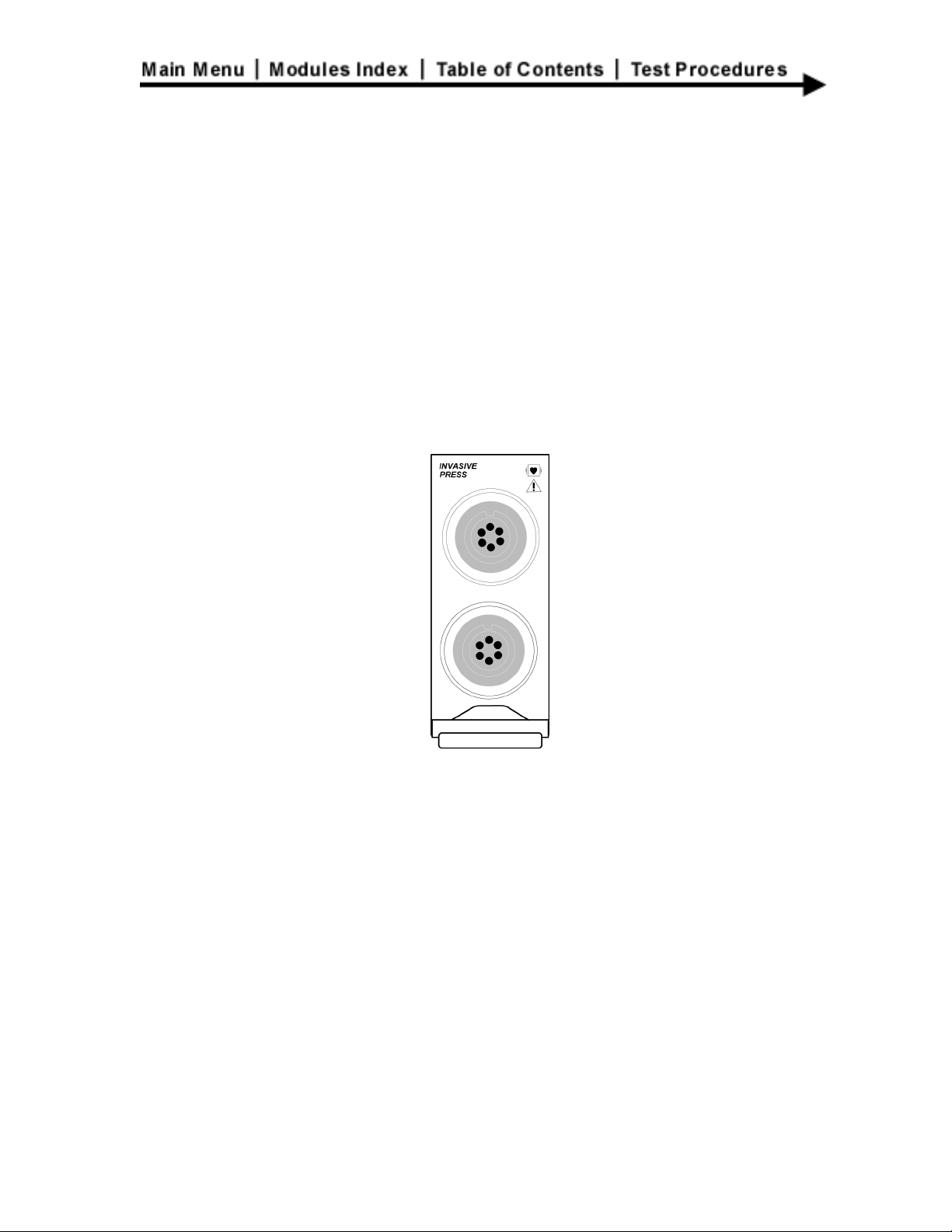
PHYSICAL
DESCRIPTION
The IP module, shown in FO-6B, occupies a single
parameter slot. The circuitry is contained on a
single, 6-layer PWA. The module contains a front
panel with connectors for one or two resistive bridge
pressure transducers. A flex circuit PWA transfers
the signals from the connectors to the rigid PWA.
The two layers of the flex circuit act as a shield for the
inner signal traces. Removable metal cans cover
the top and bottom of the PWB isolated circuitry. The
two side insulators (item 13) insulate isolated
circuitry from non-isolated circuitry, and thus ensure
compliance with patient safety requirements.

FUNCTIONAL
PRINCIPLES OF
OPERATION
Isolated Circuits
A functional block diagram of the IP Module is shown
in FO-6A. The diagram is divided into isolated
circuitry and non-isolated circuitry. The isolated
circuitry includes the EMI filters, IP front end
amplifiers and filters, A/D conversion, and isolated
control. The ISO interface and DC-DC converter
isolate this circuitry from the non-isolated core logic.
The core logic provides communication between the
system host and module through the PNet
synchronous serial interface. It also controls data
acquisition and data processing functions for the
pressure channels.
Isolated circuits are shown in the top half of FO-6A.
Signals from pressure transducers at two patient
connections are received through the module front
panel connectors and are connected to the circuit
board via a flex circuit. IP1 and IP2 are then filtered
and applied to the IP front end.
The IP front end supplies ratiometric excitation
(IPEX) to the transducers via the EMI filter and
amplifies the IP1 and IP2 input from the pressure
transducer bridge. Disconnect signals (DIS_CON)
are used to determine when a transducer has been
plugged in.
The A/D Conversion block samples analog data IP1
and IP2. A buffered version of the A/D reference is
used for transducer excitation. This allows the
readings to be isometric. The A/D converter is
controlled by the isolated control FPGA.
The ISO control FPGA receives serial commands
from the CPU and reports status and sends data
back to the CPU through the ISO interface. The ISO
interface provides an isolated asynchronous serial
communication channel between the core logic and
the isolated control FPGA.

Non-Isolated Circuits
The isolated power block consisting of +9V, +5V, -9V,
and -5V power supplies provides isolated power to
the patient connected circuitry.
Non-isolated circuits are shown in the bottom half of
FO-6A. Functional blocks include the PNet interface,
reset/failsafe, 68302 microprocessor, 8 bit memory,
and logic analyzer/test interface.
Power for the core logic (+12V and +5V), is received
through J1. The +12V is applied to the DC-to-DC
converter which powers the isolated power block.
The +5V supplies power to all non-isolated core
logic. The -12V and +3.3V power supplies are not
used on this Module.
The Module will not be damaged when plugged into
a live slot. Core logic power inputs to a module are
limited to a peak inrush current during hot-plugging.
Within 2 seconds the module responds to
identification and wakes up in a minimized power
state until registered with the system.
The PNet interface allows asynchronous and
synchronous data transfer between the core logic
and the external devices. Synchronous operation is
always used in MPS systems. Asynchronous
operation is for test and development only. The
reset/failsafe logic provides power-on reset,
processor reset and halt, and failsafe if a problem
occurs with the microprocessor. The
microprocessor controls and transfers data within
the core logic. The program memory is a FLASH
device that can be loaded with program information
from the PNET interface or the logic analyzer
interface. Data memory temporarily stores status
and monitoring data for processing.

COMPONENT
PRINCIPLES OF
OPERATION
EMI Filtering
IP Module PWA schematic SC315-447 and IP Flex
PWA schematic SC313-104 are contained here. The
first two sheets of SC315-447 show an overall block
diagram of the IP PWA.
The EMI filter circuit is shown on sheet 3 of the
schematic. Transducer signals are received on front
end connector J100 (sheet 1) with the following
pinout:
PIN NAME PIN NAME
1 IPEX2-_RAW 5 IP1+_RAW
2 IP2+_RAW 6 IPEX1-_RAW
3 IP2-_RAW 7 IPEX1+_RAW
4 IPEX2+_RAW 8 IP1-_RAW
The transducer plug shield is connected to shield
ground (SGRD). SGRD is terminated to ground (IG)
by a 10KΩ resistor. Filtering on all transducer
signals is accomplished by a ferrite core encircling
the flex, providing common mode filtering. Also,
1000 pf bypass capacitors C149 through C152 and
C154 through C157 decouple each signal to the
internal shield. These signals are clamped at ±9V
by CR13 and CR14. As shown on sheet 4, the input
signals IP1+/- and IP2+/- have additional lower
frequency common mode filtering through C125,
C126, C130, and C131, and differential mode
filtering through C122 and C147.

IP Front End
The IP front end amplifies and filters the input from
the pressure transducer bridge. The IP front end is
shown on sheet 4 of the schematic.
Pressure Channels
Excitation drivers U124-5,6,7 and U123-1,2,3 buffer
and scale AD_REF from the A/D converter to provide
a nominal transducer voltage excitation of +4.97V
(IPEX1+ and IPEX2+) for both pressure transducers.
This gives a nominal scale of 24.85 µV/mmHg at the
input, for a transducer which has a gain of
5µV/V/mmHg. Since the excitation is derived from
the A/D reference, the system is ratiometric and
variations in the reference cancel. R174, C141 and
R173 and C142 provide lead compensation for the
excitation driver.
The bridge outputs from the transducers are
received differentially through instrumentation
amplifiers U100 and U101. The dynamic range of
the channel is nominally an input pressure of ±500
mmHg. The instrumentation amplifiers have a gain
of 100. The pressure channels (IP1 and IP2) are
then passed through 4-pole, low pass, 40 Hz
Butterworth anti-aliasing filter U119, with an
additional gain of 1.638. The two pressure channels
(IP1 and IP2) are then multiplexed and buffered
where they are presented to the A/D for conversion.
An IP1 or IP2 output of ≈800 mV is equivalent to 200
mmHg.

Disconnect Detection Circuitry
DIS_CON_1 and DIS_CON_2 are buffered versions
of the common mode transducer bridge voltages.
When an IP cable is disconnected, this voltage is
pulled to the negative supply (-5V) via 10 MΩ pull-
down resistors R187 and R189. Pull-down resistors
are used on both the positive and negative inputs of
the instrumentation amplifiers to minimize errors
due to offsets currents through the transducer.
When a transducer is plugged in, the common mode
voltage is pulled up to half of the excitation voltage
(+2.5V). Disconnect signals DIS_CON_1 and
DIS_CON_2 are monitored via an A/D converter. A
disconnected cable gives a full scale A/D reading of -
2.048V, while a connected transducer is ≈ 2V.
Test/Calibration Interface
U112 consists of two double-pole double-throw
analog switches are used in front of instrumentation
amplifiers U100 and U101. These switch in
calibration signals for channel gain and offset. The
control for these signals is provided by the Isolated
Control section. With IPTESTZERO-0 low, asserting
IPTEST1-0 and/or IPTEST2-0 pulls both inputs of the
instrumentation amplifiers to ground allowing the
channel zero to be read. Releasing IPTESTZERO-0
turns on Q102 and Q103, and provides
approximately 5 mV at the junction of voltage dividers
R148-R146 and R154-R155. This voltage is applied
through the analog switches to instrumentation
amplifiers U100-3 and U101-3 when IPTEST is
selected. This voltage is equivalent to 199.8 mmHg
and used for a calibration signal. This allows the
gain of the channels to be calibrated. Additionally,
anti-aliasing filter U119 response may be checked
by using the Service Mode facility to input a step
function and monitor the transient response of the
filter output.

A/D Conversion
The A/D conversion block samples the analog data
under control of the isolated control block. This
circuit is shown on sheet 5 of the 315-447
schematic.
Reference
The reference AD_REF at TP100 for the A/D is the
4.096V internal reference provided by the MAX191
A/D converter U111. The A/D reference, scaled and
buffered at U123 and U124, provides the reference
for the transducer excitation for both pressure
transducers.
Multiplexer Control
The two pressure channels (IP1 and IP2) are
multiplexed by U102 and buffered by U122 where
they are presented to the A/D for conversion.
Clamping diodes before the A/D buffer keep the
input to the A/D within a diode drop of the supplies
(±5V). The 8-to-1 multiplexer U102 controls channel
selection of IP1, IP2, DIS_CON_1, DIS_CON_2, and
resistor networks R108-R113. The resistor
networks allow the A/D converter to monitor ±9 and 5V power supplies. The select signals, MUX0,
MUX1, and MUX2 are controlled by the isolated
control section. The isolated control section
controls the switching of the select signals, and
takes into account the acquisition and settling times
needed between A/D conversions.

Isolated Power and
Interface
Converter Characteristics
A filtered version of digital power supply +5VD (+5VA)
is used to power the A/D converter U111. The A/D is
a bipolar 12-bit sampling converter with full scale
ranging from ±2.048V. This yields approximately 4
LSBs/mmHg for the pressure channels. Digital data
is output (DOUT) serially and formatted in 2’s
complement. The conversion rate is determined by
the AD_CLK (SCLK) frequency, normally 410 kHz.
Conversion Control
Conversion is initiated by the assertion of AD_CS
and the next falling edge of the clock (AD_CLK).
These control signals are derived from the isolated
control section. Data (AD_DATA) is valid on the
AD_CLK rising edge.
The isolated power block is shown on sheet 6 of the
schematic. It provides power to the patient
connected circuitry which is isolated from earth
ground for patient safety. The isolated
communication interface is shown on sheet 7 of the
schematic. It provides an isolated asynchronous
serial communication channel between the core
logic and the isolated circuitry.
Isolated Power
The isolated power section provides patient isolation
from earth ground (compliant with UL 2601 and IEC
601) by isolating the power for the patient connected
circuitry.

DC-to-DC converter PM100 provides isolated,
unregulated power outputs of ±12VDC (+VS and -VS)
derived from the system non-isolated +12VDC
supply. L1 provides common mode filtering to
reduce noise generated by the DC-to-DC converter.
Voltage regulators driven from the isolated supply
provide regulated +5VDC, +9VDC, -5VDC, and 9VDC supplies for the isolated circuitry.
The positive regulated supplies provide open
collector PWR_OK signals which are ORd together.
A logic low signal indicates that one of the regulator
outputs has dropped by more than 5%.
The +9VDC, -9VDC and the -5VDC supplies are
scaled and monitored through the A/D converter
(R108-R111 on sheet 5).
The isolated power supply is turned on when Port A
bit 6 from the CPU (ISO_POWER_ON-0) is enabled
(active low).
Isolated Interface
Opto-couplers U105 and U106 provide a full duplex,
isolated serial channel between the non-isolated
core logic and the isolated circuitry. The isolated
control block receives data through opto-coupler
U105 and transmits on U106. Opto-coupler U107
transmits the baud clock (16x baud rate) which
provides the clock (ISO_CLK, normally 830 kHz) to
the Isolated Control. Q100, Q101, and Q105 buffer
the signals to the opto-couplers.

Isolated Control
The isolated control block is shown on sheet 8 of the
schematic. The isolated control block accepts
commands from the core logic, provides the control
for the isolated circuitry, reads input data, outputs
data, and commands a/d conversion. Sampled data
is passed back to the core logic through this
interface.
The isolated control is implemented with a fieldprogrammable gate array (FPGA) U104. EPROM
U103 stores the configuration data for FPGA U104.
This data is downloaded to U104 on power up. The
function of the isolated control block is to accept
serial commands from microprocessor U10 via the
ISO Interface and output the appropriate control
signals, AD_CS, AD_CLK, and MUX 0-3 to the
analog circuitry and to transmit sample data
(AD_DATA) and status back to the microprocessor.
This controls the MUX channel selection, the
operation of the A/D converter, and the IPTEST
signals.
Core Logic
The core logic is shown on sheets 9 through 13 of
the schematic. The core logic provides
communication between the system host and
module through the PNet synchronous serial
interface. It also controls data acquisition and data
processing functions for the pressure channels.
The module is an 8-bit version of the core logic with
one 128Kx8 RAM and 128Kx8 ROM device. The
microprocessor runs at 9.966 MHz.
PNet Interface
The PNet interface, shown on sheet 10 of the
schematic, provides the following functions:
• RS485 drivers (U7 and U8) for serial data and
clock,
• Module select and presence detection (U2),
• Module reset (U6 and U9), and
• Module synchronization.

Core signals are received on PNet connector J1
(sheet 2) with the following pin-out:
PIN NAME PIN NAME
1A,1B +5V 6B M_SELECT
2A DATA+ 7A M_PRESENT
2B DATA- 7B TXOC-0
3A,3B +3.3V 8A M_SYNC-0
4A CLK+ 8B -12V
4B CLK- 10A,10B +12V
5A,5B GROUND 1,2 GROUND
6A M_RESET
The IP module is designed to be hot-plugged, or
inserted and removed from powered systems.
Ground pins 1 and 2 are longer than the other
connector pins, thus they make first and break last to
protect circuitry. Protective impedance located on the
system backplane, in series with the modules +5V
and +12V power, limits inrush current on hotplugging or live insertion. Series impedance on
PNet control lines also limits inrush and protects
logic devices from excessive currents during a hotplug power up.
The PNet protocol defines two modes of operation:
synchronous and asynchronous. The normal mode
of operation is synchronous, with half duplex
transmitted and received data on differential signals
DATA+ and DATA-. The device transmitting the serial
data also generates differential clock signals CLK+
and CLK-. Transceiver direction for data and clock
are controlled by the 68302 processor-generated
TX_EN-0 (low true transmit enable) signal through
U2. In the synchronous mode, both data and clock
transceivers U7 and U8 are set to receive (i.e.,
transmit disabled) when fail-safe signal FS-0 is
asserted.

The alternate serial mode, full duplex asynchronous,
is entered by asserting processor generated control
bit ASYCH_EN. This mode transmits data onto the
differential signals CLK+ and CLK-, and receives
data from the differential signals DATA+ and DATA-.
The transmitter in the module is disabled unless the
module has been commanded to transmit per the
PNet protocol. The module transmitter is
immediately disabled after the last character of a
transmission has been sent.
The module select input (M_SELECT, hi true)
instructs the module to respond to identification
requests. When both M_SELECT input and
M_RESET input (hi true) are asserted, a module
performs a hardware reset.
The module present output, M_PRESENT is
connected to M_SELECT through diode CR1 to allow
a means of determining if the module is plugged
into an instrument. When M_SELECT is asserted
(pulled hi) M_PRESENT is hi true.
A low true open collector signal TXOC-0 from Q1
signifies the module transmitter is enabled. Serial
data is then transmitted in the synchronous mode.
M_SYNC is a signal used for timing purposes that
require shorter latency time than supported by the
serial data protocols. M_SYNC is not asserted by a
Module unless enabled to do so by the host. At the
time of publication, the IP Module does not drive
M_SYNC.
Reset Logic
The reset logic is shown on sheet 11 of the
schematic. Power on reset is generated by U9 when
the unit is powered up. Processor reset (RESET-0)
and halt (HALT-0) are generated by the system.
RESET-0 AND HALT-0 signals remain low for
minimum of 130 msec after all logic rail is in
specification.

External reset, processor reset, and halt signals are
low for minimum of 24 clocks when external reset
asserted. Power monitoring, processor reset, and
halt signals low when logic rail drops below
specification. they remain low for minimum of 130
msec after logic rail returns to specified range.
The reset circuit (U6-4,5,6; U6-11,12,13) provides
open drain outputs to the processor bi-directional
reset and halt signals.
Fail-Safe Logic
Fail-safe latch (U6-1,2,3; U6-8,9,10 on sheet 11)
ensures that the module enters a safe state should
the processor fail to operate correctly. The latch is
set by a low true output from the processor watchdog
timer (WDOG-0). The data transmitter is disabled
and module remains in a safe state until the latch is
cleared by a power on or external reset.
Microprocessor
The core logic design is based around the 68302
microprocessor (U10) shown on sheet 12 of the
schematic. The 68302 combines a 68000 core with
a three channel communication processor, and
system integration circuits.