

Critikon Dinamap ECG Modul Service manual

ECG MODULE
INTRODUCTION
This area contains component information about the
ECG Module (also referred to as the EKG Module).
The singlewide module provides
electrocardiographic waveforms in either 3-electrode
(Model 7322) or 6-electrode (Model 7324)
configurations. The 3-electrode configuration
derives waveforms for leads I, II, or III. It includes a
waveform cascade feature and can display one
waveform as the primary lead. The 6-electrode
configuration derives waveforms for leads I, II, III,
AVR, AVL, AVF, VA, and VB.

When 4 electrodes are connected to the patient,
waveforms I, II, III, AVR, AVL, and AVF are available
simultaneously to view and/or to record. When 5
electrodes are connected to the patient, waveforms I,
II, III, AVR, AVL, AVF, and a single V lead (chest lead)
are available simultaneously to view (maximum of 6
to display) and/or to record. When 6 electrodes are
connected to the patient, waveforms I, II, III, AVR, AVL,
AVF, and two V leads (chest leads) are available
simultaneously to view (maximum of 6 to display)
and/or to record.
Breath rate is calculated by measuring the thoracic
impedance between two electrodes. As the patient
breathes, the movement of the chest changes the
measured impedance to produce the respiration
rate.
Heart rate values are also calculated as straight or
weighted averages over the previous 5 or 10
seconds.
PHYSICAL
DESCRIPTION
The temperature port of the module allows
continuous monitoring of patient temperature using
a YSI temperature probe.
As shown in FO-8B, the module consists of the
analog PWA, ECG/temp flex assembly, digital PWA,
defib sync flex assembly, card guides, and an
enclosure, including front and rear face plates and
other metallic hardware. The enclosure and front
and rear face plates are grounded metal. The front
and rear panels are held in place by long bolts,
running from end to end. Insulating guides hold the
circuit boards into position in the enclosure, and
provide insulation from the enclosure bolts.
Sidewall insulators, necessary to maintain patient
safety requirements, insulate the module wall.
Front panel connections include a _” stereo jack for
YSI 400 Series temperature probes, an ECG
connector compatible with the recommended ECG
cables, and a 3.5 mm stereo jack connector used for
defib sync.

FUNCTIONAL
PRINCIPLES OF
OPERATION
Isolated Circuits
A functional block diagram of the ECG Module is
shown in FO-8A. The diagram is divided into
isolated circuitry and non-isolated circuitry. The
isolated circuitry includes the ECG flex connector
PWA, and either the 3-lead ECG Analog PWA 315547 (Model 7322) or the 6-lead ECG Analog PWA
315-548 (Model 7324). The isolated (ISO) interface
and DC-to-DC converter isolate this circuitry from the
non-isolated core logic.
The core logic provides communication between the
Module and the Monitor through the PNet
synchronous serial interface. It also controls data
acquisition and data processing functions for the
ECG monitoring channel.
Isolated circuits are shown in the top half of FO-8A,
sheets 1 and 2. ECG data is filtered by ECG front
end and amplified by differential amplifiers to provide
four outputs (ECG1 through ECG4) shown on sheet
1. These ECG signals are filtered by bandpass
filters and applied to the multiplexer.
The ISO control and power block serially reads ECG
data back to the CPU through the isolated interface.
An asynchronous communication channel between
the CPU and the ISO control is implemented with a
UART. Commands are decoded with control
converter U10, which sets the state of multiplexers
and switches in the isolated circuitry.
Temperature sensor circuits provide an excitation to
the YSI thermistors through a precision resistor
bridge. These signals are filtered and amplified and
sent to the A/D converter. Temperature is then
derived ratiometrically from these signals.

Non-Isolated Circuits
The isolated interface shown on sheet 2 provides an
isolated asynchronous serial communication
channel between the non-isolated core logic CPU
and the ECG isolated front end.
Respiration circuits provide an AC excitation signal
through two electrodes. The signal is modulated by
thoracic movement during normal breathing. The
signal is then demodulated, amplified, and filtered,
and sent to the A/D converter, and breath rate is
derived.
The isolated power block, consisting of isolated +VAI
(+8V nominally), -VAI (-8V nominally), +5VI, -5VI, and
+5VID power supplies, provides isolated power to
the ECG Module and the sensor connected circuitry.
Non-isolated circuits are shown in the bottom left of
FO-8A, sheet 1 and the bottom half of sheet 2.
Functional blocks shown on sheet 2 include the
PNet interface, DC-DC converter, ISO power control,
reset/failsafe, 68302 CPU, 256Kx16 data memory,
256Kx16 program memory, the model and serial
number EEPROM, and logic analyzer/test interface.
Power (+12V and +5V), is received through J1. The
+12V is applied to the DC-DC converter, which
powers the isolated circuitry. ISO power control
does not allow the DC-DC converter to power-on
until after the CPU is reset and shuts down the DCDC converter if a failsafe condition occurs.
The Module will not be damaged when plugged into
a live slot. Core logic power inputs to a Module are
limited to a peak inrush current during hot-plugging.
Within 2 seconds the Module will respond to
identification and wake up in a minimized power
state until registered with the system.

COMPONENT
PRINCIPLES OF
OPERATION
The PNet interface allows asynchronous and
synchronous data transfer between the core logic
and the external devices. Synchronous operation is
always used in MPS systems. Asynchronous
operation is for test and development only. The
reset/failsafe logic provides power-on reset,
processor reset and halt, and failsafes if a problem
occurs with the microprocessor. The
microprocessor controls and transfers data within
the core logic. The program memory is a FLASH
device that can be loaded with program information
from the PNET interface or the logic analyzer
interface. Data memory temporarily stores status
and monitoring data for processing.
Schematic diagrams SC313-108, SC313-109,
SC315-546, and SC315-548 are here. The first
sheet of the SC315-546 schematic shows an overall
block diagram of the ECG Digital PWA. The first
sheet of the SC315-548 schematic shows an overall
block diagram of the ECG Analog PWA.
Isolated
Power Block
The isolated power block is shown on sheets 8 and
9 of ECG digital PWA schematic 315-546. Power
converter PM1 converts non-isolated +12V to
isolated +VS and -VS. This power is isolated for
patient safety requirements. U101, U102, and U103
on the digital PWA are the opto-couplers that provide
isolation for communications data and the clock.
PM1 is controlled by ISO_POWER_ON from the CPU
via Q103. This signal disables PM1 if a failsafe
condition occurs. The +VS and -VS (unregulated)
voltages from PM1 are filtered by L100 and applied
to regulators U105, U106, U107, U108, and U111.

Isolated Control
Circuits
These regulators supply isolated power to ECG
analog PWA 315-548. The voltages are:
+5 VID for digital circuits
+5 VI for analog circuits
-5 VI, +VAI (+8 VDC), -VAI (-8 VDC)
Error outputs from positive regulators U105, U106,
and U111 are OR'ed together to provide PWR_OK. If
a power supply output drops 5% below the regulated
output, PWR_OK goes low, which causes the CPU
to shut down the isolated supply.
The isolated control circuits are shown on sheets 14
and 15 of ECG analog PWA schematic 315-548.
Field programmable gate array (FPGA) U103
contains the state machine, which provides an
interface between the isolated analog circuitry and
the main CPU on the non-isolated circuitry of digital
PWA 315-546. Communication is achieved through
a UART, which provides a full duplex asynchronous
serial communication channel between the CPU
and the isolated circuitry. On power up, the nonvolatile program data for the FPGA is loaded from
serial EPROM U105 into U103. After several
hundred milliseconds, the FPGA is configured and
ready to run. CLOCK for the state machine is a 5.9
MHz signal provided from the CPU via opto-couplers
located on the digital PWA.
Commands are sent serially (via opto coupler for
isolation) through DATA_IN. Data is sent back to the
CPU by DATA_OUT and is also optically isolated (on
the digital PWA).
The state machine responds to commands to
perform A/D conversions or to change the states of
multiplexers or switches. It provides the control for
the serial A/D interface, a 1.5 MHz clock to the A/D
(ADC_SCLK), and proper control signals AD_CNVST
to initiate a conversion.

ECG/RESP
Inputs
Digital signals are also read back on command to
provide the CPU with status information. Board
configuration (single lead, part number 315-547 or
multi lead, part number 315-548) is determined by
the PWA_CFG bits located on sheet 15 of analog
PWA schematic 315-548, and provided to the CPU
on command. Pacer detection status is another
status that the CPU monitors.
The state machine also derives the respiration clock
signals (RESP_CLK and DM_CLOCK) and switched
capacitor filter clock (LPF_CLK) as divided down
versions of the main 5.9 MHz clock.
Three lead (3-electrode) and six lead (6-electrode)
cables are available for ECG. The 3-electrode cable
provides a single lead configuation with Leads I, II or
III available. The 6-electrode cable provides multiple
leads with up to 8 leads available: I, II, III, AVR, AVL,
AVF, VA and VB. The 6-electrode cable may be used
with 3, 4 , 5, or 6 electrodes. (Refer to the EKG
section of the Operation Manual for a description of
which leads are available with the number of
electrodes connected.) In single lead (3-electrode
cable), signals RA, LL, and LA are used. In multi
lead (6-electrode cable), signals RA, LL, LA, RL, C1,
and C2 are used.
The cables recommended by JJMI are shielded and
provide 1k ohm series (safety) resistors internal to
the cable which is part of the current limiting
defibrillator protection circuitry.
The signals are input to the flex PWA 313-108. Gas
surge arrestors located on the PWA provide lead-tolead defibrillator protection. In addition, a passive
R/C network located on this PWA provides the first
stage of high frequency filtering for EMC and ESU
interference rejection.

RESP Input
The signals are then applied to analog PWA (part
number 315-548 for multi lead, or part number 315547 for single lead) via J101.
The RESP input is shown on sheet 10 of ECG
analog PWA schematic 315-548. Of the ECG
signals, RA, LA, and LL are also used by the
respiration circuit. Respiration is achieved by
coupling an excitation signal (61.5 kHz, well outside
the bandwidth of normal ECG signals) onto two of
these signals. When respiration is using Lead I, the
excitation is coupled onto RA and LA. When
respiration is in Lead II, the signal is coupled onto
RA and LL.
The excitation signal is coupled onto the EKG leads
through coupling capacitors C179, C180, and C200.
The coupling capacitors isolate the ECG signal from
being loaded down by the respiration circuit. Photo
relay U121 determines which lead is selected. T100
provides a differential excitation source. CR108,
CR112, and CR113 provide clamping protection for
transients.
ECG_RESP_INPUT
The ECG_RESP_INPUT is shown on sheet 2 of
ECG analog PWA schematic 315-548. The ECG
signals are passively filtered by R/C network R314,
R315, R316, R372, R373, R374, C201, C257, C258,
C259, C221, and C222 at 5 kHz for interference
rejection of high frequency noise and ESU. Also, the
excitation signal for respiration signal is attenuated
and kept out of the ECG channel circuitry and pace
detection circuitry. Protection diodes CR114-116
and CR125-127 protect against transients during
both defibrillation and ESU events. R368 through
R371 and R310, R212, and R213 are light pullup
resistors which limit DC current through the
electrodes and are used to determine when an
electrode has become disconnected from the
patient.

ECG Front End
The ECG front end is shown on sheet 3 of ECG
analog PWA schematic 315-548. The filtered ECG
signals LA_FLT, RA_FLT, LL_FLT, RL_FLT, C1_FLT
and C2_FLT are buffered at U122 and U138 and
then multiplexed at U132 to be read by the A/D.
These signals are used to help determine which
electrodes are connected to the patient. These
signals (or sums of these signals in the case of
chest leads) are also differentially applied to the
instrumentation amplifiers U119, U126, U133, and
U134 with gains of X10, and create the first stage of
the four ECG channels.
The signals also generate a common mode nulling
signal by summing all the necessary leads at U127
and U136 for a given mode, inverting the sum, and
amplifying and applying the null signal at the
selected reference or driven signal at U137. The
signals selected at U127 to generate the common
nulling signal depend on which electrodes are
available and which mode the module is in - single
lead or multi lead.
Additionally, U128 provides the means to make ECG
instrumentation amplifier U119 selectable between
LEAD I, II, or III. U135 and U122-8 provide the
means for applying various test signals to the ECG
channels and the pacer detection circuit. Signals at
U127-5,6,7 are also used in various test modes
using the Service Mode facility.

Pace Detector
The pace detector and filter are shown on sheets 4
and 9 of ECG analog PWA schematic 315-548.
Pacer signals present on ECG waveforms are
detected by the pacer detection circuitry. Any of the 4
ECG channels (outputs of the instrumentation
amps) may be used to detect pacers. The channel
is selected at U125, sheet 4. When a paced ECG
waveform is present and pace detection is enabled,
the pace detector circuit will detect the presence of a
pacer pulse and blank the ECG channels during the
pacer pulse to suppress pacer spikes in the ECG
channels.
The detector on sheet 9 consists of a high gain
bandpass filter at U113 (200Hz to 5kHz) which
rejects both respiration excitation remnants, and 60
Hz and is sensitive mainly to waveforms with pacer
signals present. When a pacer pulse is present, the
output goes above or below the limits set by the
window comparator at U108 and causes
PD_TRIGGER to go true to indicate the presence of
a pacer.
ECG Channel Filters
When enabled, the detection of a pacer causes the
ECG channels to be blanked. This is achieved by
the opening of the channels at U124 and the
channel hold capacitors, C189,188, 165, 194
(sheets 5 through 8). The channels are blanked
during the entire duration of a pacer pulse.
ECG channel filters are shown on sheets 5 through
8 of analog PWA schematic 315-548. The circuits for
the ECG bandpass filters are duplicated for the four
channels on sheets 5 through 8. The description of
channel 1 (on sheet 5) is similar for the other three
channels.

The bandpass filtering is achieved mainly through 8pole switched capacitor filter U110, which has a
cutoff at 115 Hz and through integrator circuit U11112,13,14, which strips off the DC component of the
ECG waveform. This is the MAIN anti-aliasing filter
for the ECG channels. (Sampling frequency in
normal use is 1200 Hz.) The cutoff frequency of the
swithed capacitor filter is determined solely from its
input clock frequency (LPF_CLK, 11.5kHz). This
clock signal divided by 100 gives the 115 Hz
lowpass response. The resulting frequency
response of the entire bandpass filter section is
approximately 0.05-115 Hz with a gain of 12. With
the earlier instrumentation amplifier stage this give
an approximate ECG channel gain of 120. The
filtering stage prior to the switched capacitor filter at
U111 provides low pass filtering and anti-aliasing
prior to the switched capacitor filter and has an
approximate 3dB point at 1kHz and a gain of 5. The
filtering stage after the switched capacitor filter at
U111-8,9,10 also has a 1kHz 3dB point for
eliminating any clock noise from the previous filter
stage and has gain of 2.4. Thus the X5 and X2.4
give the gain of 12 in this stage.
Q103 and R218 provide a means to quickly charge
the integrator stage (0.05 Hz high pass stage) to
reestablish a new baseline during lead switching or
new lead attachment. The output of the channel at
ECG1_OUT is then routed to main mux U102 to be
used by the A/D converter.

Respiration
and Filters
The ECG respiration circuits and filters are shown
on sheets 10 and 11 of ECG analog PWA schematic
315-548. The respiration clock RESP_CLK controls
the analog switch U114 providing an excitation
signal of 61.5kHz from quiet reference U120 to buffer
U115, where it is filtered and then drives transformer
T100 where the signal driven differentially on the two
selected respiration leads RA_RESP and LA_RESP
or LL_RESP. RESP_LEAD_SEL selects the
respiration leads through U121 (LEAD I or LEAD II).
DM_CLOCK, slightly off phase from RESP_CLK, is
used to provide a synchronous demodulator with
U114 and U115. The demodulator rectifies the
waveform and the signal is then filtered through a
bandpass filter (sheet 11) with a frequency response
of 0.1-5 Hz.
As the patient's chest rises and falls due to
breathing, the impedance of the chest typically
changes by several ohms. The excitation is a
constant current source so a change in impedance
causes a change in amplitude of the voltage which
is sensed at T100-1. Essentially the carrier
(excitation signal) is slowly AM modulated by thoracic
movement. The demodulation allows the slow
respiration signal to be detected. The filter
eliminates the 61.5kHz carrier signal and leaves the
respiration signal. The filter is implemented in
several stages at U109 with a total gain of x600.
RESP_OUT then goes to the main mux where it is
read through the A/D converter. Similar to the ECG
channel, Q102 allows the integrator to quickly charge
to a new baseline during lead switching and new
lead attachment.

Temperature
Circuits
RESP_BL_OUT (respiration baseline) on sheet 10
is a signal derived from the diode-rectified carrier
(asynchronous demodulation) signal at CR111. The
impedance of the chest movement during breathing
is a small dynamic change of several ohms riding
on top of a relatively large impedance or baseline
(typically 100-2000 ohms). The RESP_BL_OUT
gives an indication of this baseline impedance. If
this signal becomes too large, it is an indication that
a respiration electrode has fallen off or is dried out
and has become too large of an impedance.
U114-2,9 and R152,C139, R196 and R236 and
Q104 provide the means to test the respiration
circuitry. Using the Service Mode facility, a test can
be commanded to run which uses these
components to stimulate the respiration circuit with a
dynamic impedance (approximately 10 ohms) that is
square wave in nature.
The temperature circuits are shown on sheet 12 of
ECG analog PWA schematic 315-548. The
temperature circuit is used to monitor YSI 400
series temperature probes. It works by determining
the ratio of the YSI probe resistance to that of a
precision reference resistor. This is accomplished
through a voltage divider circuit. An excitation voltage
(TEMP_EXC, 0.385 volts nominally) at U107-1, is
generated across the reference resistor (R154) and
the probe thermistor (in series with the reference
resistor). The excitation voltage and the voltage
across the thermistor are filtered and amplified with
a gain of 5.44 at U106, 107 and measured by the A/D
converter. The ratio of the reference resistor to the
thermistor resistor can be determined from the
measured voltages.

Once the resistance of the YSI probe is determined,
the temperature is found, by means of a look up
table, from the thermistor's electrical resistance
versus temperature relationship. The electrical
thermistor data is provided by YSI.
Relay K100 allows a test resistor (R153) to be
switched in to verify the temperature circuitry. When
the relay is de-energized the excitation is applied to
the external probe at TEMP_HI. In the energized
state the excitation is applied to the test resistor.
The voltage at U106-9 at R153 is also monitored to
verify the correct operation of the relay contacts.
TEMP_HI and TEMP_RET via J101 reach the front
panel of the ECG module at the 1/4" stereo jack by
Flex PWA 313-108. This flex circuit contains bypass
caps which help filter out high frequency interference
in the temperature signal path.
At U106-7,-10,-11,-12, other inputs included are
scaled versions of the power supply voltages. The
voltages are sent to the A/D converter, and are used
to monitor the analog supply voltages. Using the
Service Mode facility, the self-test mode can be
initiated and resistor values and derived
temperatures can be observed.

Multiplexer and
A/D Converter
The multiplexer and A/D converter are shown on
sheet 13 of ECG analog PWA schematic 315-548.
These circuits sample analog ECG data and provide
this data serially to the CPU. EMUX, ECG1 through
ECG4, TMUX and respiration outputs are applied to
analog multiplexer U102. The multiplexer output is
selected by MUX (2:0), and the multiplexed output is
applied to buffer U100. This signal is clamped at +/5VI by CR100. The buffer output is applied to A/D
converter U101, which is clocked by ADC_SCLK_0
(1.5 MHz). The digital data (ADC_DATA) is clocked
out of the A/D converter serially by ADC_CLK and
sent to the CPU. The A/D converter also provides a
stable reference voltage (3.0V VREF) for the
temperature circuit on the analog PWA.
Defibrillator
Synchronization
Interface
The defibrillator synchronization interface is a nonisolated signal input/output meant only for
connection to another medical device that is
compliant with UL 2601/IEC 601-1. Connection to a
non-compliant device could result in a safety risk by
exceeding current limits.
The defib sync connector provides an analog ECG
waveform output. It also accepts a synchronization
signal (marker input) from defibrillators that provide
this feature. If a synchronization signal is detected a
marker is placed on the primary lead waveform
displayed by the Monitor. The analog ECG waveform
signal is a high level (1V/mV) representation of the
primary lead.
The defib sync connector is a three-conductor 3.5
mm stereo jack that mates with a 3.5 mm stereo
plug (Shogyo SPY 1011, Shogyo SPY 1012, or
equivalent). Cable construction should be shielded,
3 conductor with PVC insulation or equivalent
insulating material.
Pin Out:
Tip Marker input
Ring ECG analog output
Sleeve Signal return
ECG Analog output specifications, implemented with
10-bit DAC U104 and filter circuit of U110, on the
digital PWA:
Scale Factor 1V/mV
Output
Impedance/Short
Circuit Protection
Bandwidth 0.5 Hz-100Hz
1k ohm

The sync marker input is compatible with the HP
defibrillators. The marker signal is active when the
input is driven below ground. A pullup resistor
allows this input to be driven by an open collector
output. The input must be driven below -1V to be
detected as a marker. The input is pulled up to +5V
by a 20k ohm resistor. Therefore, the output
impedance of the driving device must be such that
the input can be driven below -1V.
Marker input specifications, implemented at U100 on
the digital PWA:
Input Range +5V to -12 V
Trip Voltage Range 0V + 1V
Minimum Marker
Pulse Duration
Protection diodes clamp any input to +5V on the high
side or to -12V on the low side. A 1k series resistor
limits current during any over voltage condition.
10 ms
The stereo jack provides two shunting contacts for
sync cable detection. When a plug is inserted, the
contacts separate. One of these floating contacts is
used to sense a connected plug. CONNECTED-0
indicates to the CPU that a plug has been inserted
into the front panel connector.

Isolated Interface
Core Logic
Opto-couplers U101 and U102 shown on sheet 8 of
ECG digital PWA schematic 315-546 provide a full
duplex, isolated serial channel between the nonisolated core logic and the isolated circuitry. The
isolated control block, located on sheet 14 of ECG
analog PWA 315-548 receives data through optocoupler U101 and transmits on U102. Opto-coupler
U103 transmits the baud clock, which provides the
5.9 MHz clock (ISO_CLK) to the Isolated Control
State Machine. Q100, Q101, and Q102 buffer the
signals to the opto-couplers. Q102 is pulled up to
+5V to speed up the rising edge of TX_CLK.
The core logic is shown on sheets 2 through 6 and
sheet 8 of ECG digital PWA schematic 315-546. The
core logic provides communication between the
system host and the ECG Module through the PNet
synchronous serial interface. The Module is a 16-bit
version of the core logic with two 128K x 8 RAM and
two 128K x 8 ROM devices. The microprocessor
runs at 23.646 MHz.
PNet Interface
The PNet interface, shown on sheet 2 of the
schematic, provides the following functions:
• RS485 diffeential drivers (U7 and U8) for serial
data and clock,
• Module select and presence detection (U2),
• Module synchronization.
Core signals are received on PNet connector J1
(sheet 1) with the following pin-out:
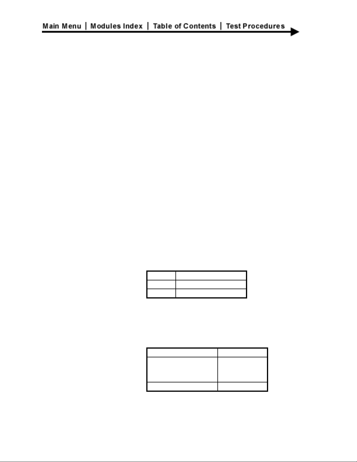
PIN NAME PIN NAME
1A,1B +5V 6B M_SELECT
2A DATA+ 7A M_PRESENT
2B DATA- 7B TXOC-0
3A,3B +3.3V 8A M_SYNC-0
4A CLK+ 8B -12V
4B CLK- 10A,10B +12V
5A,5B GROUND 1,2 GROUND
6A M_RESET
The ECG Module is designed to be hot-plugged, or
inserted and removed from powered systems.
Ground pins 1 and 2 are longer than the other
connector pins, thus they make first and break last to
protect circuitry. Protective impedance located on the
system backplane, in series with the Module’s +5V
and +12V power, limits inrush current during live
insertion. Also series impedance on PNet control
lines limits inrush current and protects logic devices
from excessive currents during a hot-plug power up.

The PNet protocol defines two modes of operation:
synchronous and asynchronous. The normal mode
of operation is synchronous, with half duplex
transmitted and received data on differential signals
DATA+ and DATA-. As shown on sheet 2 of the
schematic, the device transmitting the serial data
also generates differential clock signals CLK+ and
CLK-. Transceiver direction for data and clock are
controlled by the 68302 processor-generated TX_EN0 (low true transmit enable) signal through U2. In the
synchronous mode, both data and clock transceivers
U7 and U8 are set to receive (i.e., transmit disabled)
when fail-safe signal FS-0 is asserted.
The alternate serial mode, full duplex asynchronous,
is entered by asserting processor generated control
bit ASYCH_EN. This mode transmits data onto the
differential signals CLK+ and CLK-, and receives data
from the differential signals DATA+ and DATA-. The
transmitter in the Module is disabled unless the
Module has been commanded to transmit per the
PNet protocol. The Module transmitter is immediately
disabled after the last character of a transmission
has been sent.
The Module select input (M_SELECT, hi true)
instructs the Module to respond to identification
requests. When both M_SELECT input and
M_RESET input (hi true) are asserted, the Module
performs a hardware reset.
The Module present output, M_PRESENT is
connected to M_SELECT through diode CR1 to allow
a means of determining if the Module is plugged into
an instrument. When M_SELECT is asserted (pulled
hi) M_PRESENT is hi true.
Module transmitter open collector signal TXOC-0 from
Q1 signifies the Module transmitter is enabled. Serial
data is then transmitted in the synchronous mode.
M_SYNC is used for timing of shorter latency periods
than supported by the serial data protocols. A Module
only asserts M_SYNC when enabled by the host.

Reset Logic
The reset logic is shown on sheet 3 of the
schematic. Reset logic U9 generates a power-onreset when power is applied. RESET-0 and HALT-0
signals remain low for minimum of 130 msec after
all logic voltages are in specification.
External reset, processor reset, and halt signals are
low for minimum of 24 clocks when external reset is
asserted. Power monitoring, processor reset, and
halt signals are low if logic voltages drop below
specification. They remain low for minimum of 130
msec after logic voltages return to the specified
range.
The reset circuit consisting of U6b and U6d provides
open drain outputs to the processor bi-directional
reset and halt signals.
Fail-Safe Logic
Fail-safe latch (U6a and U6c) ensures that the
Module enters a safe state if the processor fails to
operate correctly. The latch is set by a low true output
from the processor watchdog timer (WDOG-0). The
data transmitter is disabled, isolated power is shut
down, and the Module remains in a safe state until
the latch is cleared by a power on or external reset.
Microprocessor
The core logic design is based around the 68302
microprocessor (U10) shown on sheet 4 of the
schematic. The 68302 combines a 68000 core with
a three channel communication processor, and
system integration circuits.

The left side of the CPU contains clock interfaces
to/from the PNet, port A, and port B to various circuits
in the core logic, reset, and halt interface. The IRQ
ports are not used. The right side of the CPU
contains address lines, data lines, and chip select
outputs. The 68302 operates with a statically
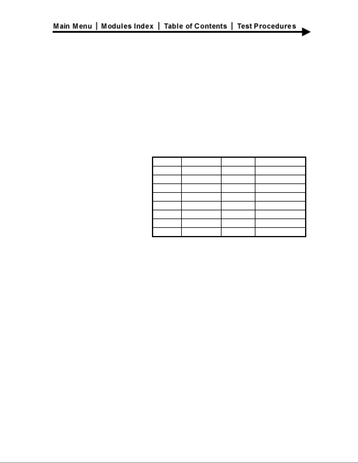
defined 8-bit wide bus. The following resources are
used for specific Module functions:
CHIP SELECTS LOGIC
CS0-0 FLASH ROM
CS1-0 STATIC RAM
SERIAL COMM CHANNELS
SCC1 PNET
[RXD1, TXD1, RCLK1, TCLK1,
CTS1-0, RTS1-0]
SCC2 ASYNC DEBUG [RXD2,TXD2]
SCP SERIAL EEPROM
[SPRXD,SPTXD,SPCLK]
TIMER1 SYSTEM TIMEBASE
PARALLEL IO / SPECIAL PURPOSE IO BITS
PA2 CHIP SELECT TO SERIAL EEPROM
PA5 ASYCN_EN (PNET MODE SELECT)
PA6 POWER MANAGEMENT CONTROL
PB5 /TIN2 TIMEBASE INPUT FOR EXTERNAL
MEMORY / SYSTEM CONFIG
PB7 WATCHDOG TIMER OUTPUT
Program Memory
Program memory consists of two 8-bit flash ROMs
U5 and U11 shown on sheet 5 of the schematic.
The ROM is configured for 128Kx16 (2048k bit). The
ROM is not socketed and can not be removed for
programming. The ROM can be flash-programmed
via the logic analyzer interface or the PNET
connector.

Data Memory
Data is stored in two 8-bit static RAMs U3 and U12
shown on sheet 5 of the schematic. These RAMs
are configured as 128Kx16. This RAM is cleared
when power is removed.
Non-Volatile Memory
Serial EEPROM U1 shown on sheet 5 of the
schematic is a 128-byte PROM that provides nonvolatile storage for model and serial number
information and parameter user interface data which
must travel with the Module. The 68302 synchronous
communication port (SCP) is used to access the
EEPROM.
Logic Analyzer/Test Interface
The logic analyzer/test interface is shown on sheet 6
of the schematic. The core logic includes an
interface to bring signals required for external ROM
access, logic analyzer interface, and a debug serial
channel to a single connector.
The external ROM access allows an off board ROM
(8 bit) or ROMs (16 bit) to replace the FLASH devices
at address 0. Address, data, and control signals
required for this function are included on the LA/T
connector.
All signals needed for a Hewlett Packard model
16500 logic analyzer or equivalent to perform bus
state analysis and disassembly are included on the
LA/T connector.
The 68302 SCC2 serial transmit and receive data
signals are included on the LA/T connector.
 Loading...